Analysis of Circuit Simulation Considering Total Ionizing Dose Effects on FinFET and Nanowire FET


1
Department of Electronic Engineering, Korea National University of Transportation, Room No. 307, IT Building, 50 Daehak-ro, Chungju-si, Chungbuk 27469, Korea
2
Department of IT Energy Convergence (BK21 FOUR), Korea National University of Transportation, Room No. 307, IT Building, 50 Daehak-ro, Chungju-si, Chungbuk 27469, Korea
*
Author to whom correspondence should be addressed.
Appl. Sci. 2021, 11(3), 894; https://doi.org/10.3390/app11030894
Submission received: 13 December 2020
/
Revised: 11 January 2021
/
Accepted: 18 January 2021
/
Published: 20 January 2021
(This article belongs to the Special Issue Device Modeling for TCAD and Circuit Simulation)
Abstract
:In this study, we analyzed the total ionizing dose (TID) effect characteristics of p-type FinFET and Nanowire FET (NW-FET) according to the structural aspect through comparison of the two devices. Similar to n-type devices, p-type NW-FETs are less affected than FinFETs by the TID effect. For the inverter TID circuit simulation, both n- and p-types of FinFET and NW-FET were analyzed regarding the TID effect. The inverter operation considering the TID effect was verified using the Berkeley short-channel insulated-gate FET model (BSIM) common multi-gate (CMG) parameters. In addition, an inverter circuit composed of the NW-FET exhibited a smaller change by the TID than that of an inverter circuit composed of the FinFET. Therefore, the gate controllability of the gate-all-around (GAA) device had an excellent tolerance to not only short-channel effects (SCE) but also TID effects.
1. Introduction
Radiation hardening on semiconductor devices is a critical issue in various fields including radiation therapy, space, and nuclear reactor processes. The characteristics of devices change when they are exposed to a radiation environment. Designs, processes and shielding to reduce radiation effects are actively being studied in [1,2,3,4]. However, the research on the radiation effect in a single device is still insufficient. Single event effects (SEE), total ionizing dose (TID) effects, soft error rate (SER), displacement damage (DD), and multiple bit upsets (MBU) lead to the obstruction of the reliable operation of semiconductor devices due to radiation [5,6,7,8,9]. The TID effect causes the issue of changing the electrical properties of semiconductor devices due to the hole trap. When the particles pass the dielectric area, electron–hole pairs (EHP) are generated. Electrons with relatively fast mobility exit the dielectric region, but holes with low mobility have some holes trapped at the existing trap site, which increases the leakage current and causes a threshold voltage (VT) shift [10]. Therefore, the device reliability is degraded. Nanoscale devices can be further affected by other static and dynamic parameters by the TID effect [11]. However, it is challenging to analyze the exact radiation effect due to the trap recovery of the irradiated device from the measurement [12,13]. Therefore, the TID phenomenon should be analyzed only by a simulation.
VTs has been used in the industry to continue the complementary metal–oxide–semiconductor (CMOS) scaling. However, critical issues such as the short-channel effect (SCE), VT roll-off, and parasitic resistance emerge upon the FinFET scaling [14]. To alleviate these issues, Nanowire FET (NW-FET) has strong gate controllability and has been proposed to replace the FinFETs [15,16]. The better gate controllability provided by the gate-all-around (GAA) structure can overcome the SCE problem and enable a more aggressive gate length scaling than that for the FinFETs [17,18,19,20]. Therefore, it is a promising solution for device miniaturization [21]. Thus, studies to mitigate the radiation effect of devices with this structure are required. In this study, TID simulations of a FinFET and NW-FET were carried out to analyze the element with a larger TID effect, according to the device structural part. This study was carried out by comparing the structural elements of the oxide area and gate controllability. Accurate TID simulation results were compared by calibrating the current and device sizes of the NW-FET and FinFET.
As the oxide area increases, more EHP occurs and the number of trapped holes increases. However, despite the larger oxide area of the NW-FET than the FinFET, the VT did not change significantly, and the device appeared to be more resistant to radiation. It is shown by introducing the GAA structure, that the higher the gate controllability, the more the TID effect can be suppressed in the oxide region. In addition, the FinFET and NW-FET affected by the TID were extracted using a Berkeley short-channel insulated-gate FET (BSIM) common multi-gate (CMG) and applied to an inverter circuit to perform the simulation.
2. Methodology of TID Simulation
2.1. Device Structure Design
The TID effects of an NMOS FinFET and NW-FET have been analyzed [22]. In this study, we analyze the TID effect of PMOS devices. The PMOS NW-FET was stacked in five stages to match the current and device size to those in the NMOS device study. The FinFET and NW-FET were similarly constructed by the three-dimensional (3D) technology computer-aided design (TCAD) simulation tool. The PMOS FinFET was designed as an equal NMOS considering the International Technology Roadmap for Semiconductors (ITRS) [23]. Figure 1 shows the TCAD structures of the FinFET and NW-FET.
The devices were made with a silicon body and the n- and p-types dopant was phosphorus and boron. The device channel insulator materials were deposited SiO2 and HfO2. The ID-VG characteristics were calibrated for an accurate comparison of the TID effects. Table 1 and Table 2 show each design’s parameters and the initial VT characteristics of the FinFET and NW-FET, respectively.
2.2. Condition of TID Simulation
For the TID simulation, we used the Silvaco’s Victory Device platform [24]. The Klaassen model was applied to the TID simulation to reflect electron and hole mobilities, trap parameters, recombination parameters, etc. [25,26,27,28,29]. In the TID simulation, the insulator region’s trap–detrap model parameters were used as in [30]. The simulation was performed precisely, as the interface trap between SiO2 and HfO2 was calculated by using an interface trap parameter between the insulators. In the TID simulation, γ-ray irradiation obtained using a 60Co source was used [31]. Each device was irradiated at 1 rad/s. The simulation was carried out at 100 krad, 1 Mrad, 10 Mrad, and 100 Mrad.
3. TID Simulation Results and Procedure of Compact Modeling with TID
Figure 2 shows the PMOS device’s electrical characteristics according to the total dose. VT was extracted when the drain absolute current was 0.1 μA using the constant current method, as shown in Figure 2. As the holes were trapped in the insulator region, VT was shifted. The electrical properties further changed with the increase in the radiation dose.
Figure 3 shows the VT shift for each TID for both FinFET and NW-FET. The result before 10 Mrad shows a large change in the VT of PMOS devices, but the result is reversed at 100 Mrad. Also, the VT variation of n-type and p-type devices is about several mV. In the case of planar MOSFET, it is known that the PMOS device is affected more by the TID effect due to the interface trap. However, in the case of nanoscale 3D-structure devices, the influence of the interface trap is reduced because of the short channel length, and the VT variation of n-type and p-type is similar. In addition, the more a device has a strong gate controllability, the less variation in the TID effect [32,33]. The NW-FET exhibits a smaller VT shift than that of the FinFET. The NW-FET has a wider oxide area than FinFET. Thus, NW-FET had to be more affected by a TID effect and exhibit a larger VT shift than FinFET. However, the NW-FET was less affected due to the superior gate controllability. This is suppressed not only the SCE problem, but also the TID effect issue [34]. Structurally, the NW-FET insulator area was larger (96.1 nm2) than that in the FinFET. However, contrary to the expectations, the NW-FET had a smaller TID effect than that of FinFET. Therefore, the gate controllability is more important in the TID effect suppression than the oxide area.
The simulation of TID circuits requires a very long time period because of the numerous calculations. However, the spice circuit simulation method, which extracts and executes BSIM parameters, can check results faster than the conventional TCAD circuit simulation. Thus, for the circuit simulation, parameters of the BSIM, widely used in the industry as a standard compact model, were extracted. Figure 4 shows a flow chart of parameter extraction considering the TID characteristics. TID simulation data from the Victory Device platform were extracted using various BSIM CMG parameters. The extracted data were applied to the circuit simulation considering the TID.
4. Circuit Characteristics with the TID Effect
To extract the data for the inverter circuit simulation, calibration with the existing TCAD TID simulation data using BSIM CMG parameters was carried out. Figure 5 shows the results of the calibration of the electrical characteristics of the FinFET and NW-FET with the BSIM CMG parameters. The electrical properties of the FinFET and NW-FET fit well with the data extracted by the BSIM CMG parameters. In addition, the TID simulation data in Figure 2 were extracted using the BSIM CMG parameters according to the radiation dose.
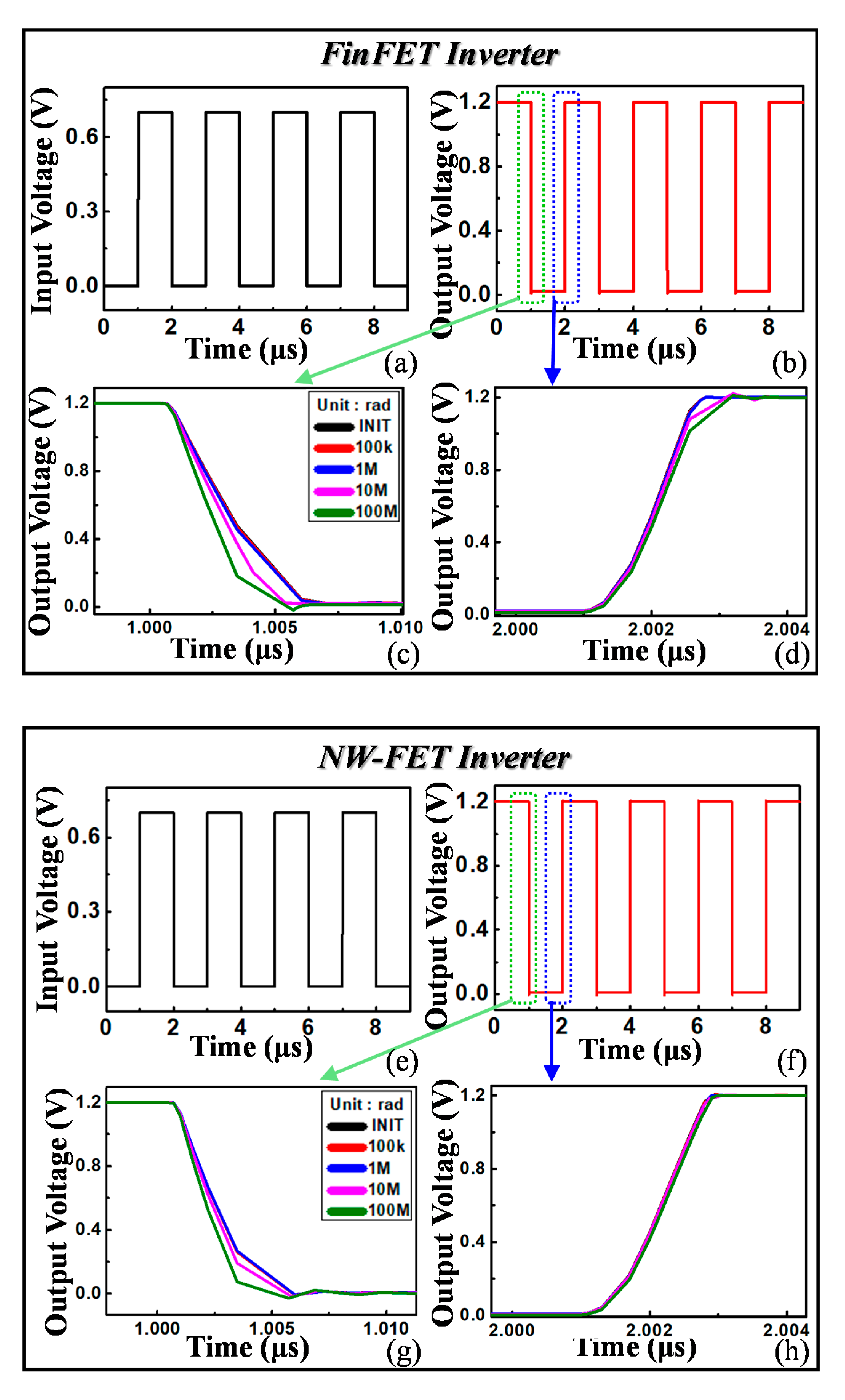
Figure 6 shows the device inverter operating characteristics according to the cumulative radiation dose. Larger switching point variations are observed with the increase in the total dose. Owing to the VT shift of NMOS, the falling edge of the inverter operation causes a faster descent, while the VT shift of PMOS causes a slow rise. Therefore, the TID effect changes the operating characteristics of the inverter and degrades the reliability. In addition, the FinFET inverter operation is more shifted than that of the NW-FET by the TID effect. The difference originates from the different gate controllability. The NW-FET inverter operation has a smaller variation with the TID than that of the FinFET inverter operation owing to its high gate controllability.
5. Conclusions
The NW-FET device exhibited a smaller ionizing radiation sensitivity than that of the FinFET device. The NW-FET had a larger insulator area than that of the FinFET, approximately 96 nm2. However, the NW-FET was less affected by the TID effect than the FinFET. The structure with a larger gate controllability confirmed that the TID effect can be effectively overcome. To improve the gate controllability method, a GAA structure and high-k dielectric materials have to be introduced. In addition, we not only analyzed the effect of the TID on the device but also applied it to the inverter using the BSIM CMG parameter reflecting the TID. The TID effect changed the operating characteristics of the inverter and degraded the reliability. However, the NW-FET inverter operation had a smaller variation with the TID than that of the FinFET inverter operation because of its high gate controllability. Therefore, NW-FET devices are tolerant to the TID, which improves the circuit operation stability in radiation environments.
Author Contributions
Carried out the simulation and methodology, H.W.; Writing—Original draft, H.W.; design figures, H.W.; was responsible for project administration, M.K.; supervision, M.K.; proofreading of the manuscript, M.K.; funding, M.K. All authors have read and agreed to the published version of the manuscript.
Funding
This research was supported by the MOTIE (Ministry of Trade, Industry and Energy (10085645) and KSRC (Korea Semiconductor Research Consortium) support program for the development of the future semiconductor devices and in part by Basic Science Research Program through the National Research Foundation of Korea (NRF) funded by the Ministry of Education (2018R1A6A1A03023788) and in part by Korea Institute for Advancement of Technology (KIAT) grant funded by the Korea Government (MOTIE) (N000P0008500, The Competency Development Program for Industry Specialist) and in part by National R&D Program through the National Research Foundation of Korea(NRF) funded by Ministry of Science and ICT(2020M3F3A2A01085755).
Institutional Review Board Statement
Not applicable.
Informed Consent Statement
Not applicable.
Data Availability Statement
Data sharing not applicable.
Acknowledgments
The authors thank Ilsik Ham for his technical advice and feedback regarding this paper.
Conflicts of Interest
The authors declare no conflict of interest.
References
- Leroux, P.; Van Koeckhoven, W.; Verbeeck, J.; Van Uffelen, M.; Esqué, S.; Ranz, R.; Damiani, C.; Hamilton, D. Design of a MGy radiation tolerant resolver-to-digital convertor IC for remotely operated maintenance in harsh environments. Fusion Eng. Des. 2014, 89, 2314–2319. [Google Scholar] [CrossRef]
- Haddad, N.F.; Kelly, A.T.; Lawrence, R.K.; Li, B.; Rodgers, J.C.; Ross, J.F.; Warren, K.M.; Weller, R.A.; Mendenhall, M.H.; Reed, R.A. Incremental enhancement of SEU hardened 90 nm CMOS memory cell. IEEE Trans. Nuclear Sci. 2011, 58, 975–980. [Google Scholar] [CrossRef]
- Clark, L.T.; Mohr, K.C.; Holbert, K.E.; Yao, X.; Knudsen, J.; Shah, H. Optimizing radiation hard by design SRAM cells. IEEE Trans. Nuclear Sci. 2007, 54, 2028–2036. [Google Scholar] [CrossRef]
- Gatti, U.; Calligaro, C.; Pikhay, E.; Roizin, Y. Radiation-hardened techniques for CMOS flash ADC. In Proceedings of the IEEE International Conference on Electronics Circuits and Systems, Marseille, France, 7–10 December 2014; pp. 1–4. [Google Scholar]
- Verbeeck, J.; Van Uffelen, M.; Steyaert, M.; Leroux, P. 17 bit 4.35 mW 1 kHz delta sigma ADC and 256-to-1 multiplexer for remote handling instrumentation equipment. Fusion Eng. Des. 2013, 88, 1942–1946. [Google Scholar] [CrossRef]
- Cao, Y.; Cock, W.D.; Steyaert, M.; Leroux, P. A 4.5 MGy TID-tolerant CMOS bandgap reference circuit using a dynamic base leakage compensation technique. IEEE Trans. Nuclear Sci. 2013, 60, 2819–2824. [Google Scholar] [CrossRef] [Green Version]
- Virmontois, C.; Goiffon, V.; Magnan, P.; Girard, S.; Inguimbert, C.; Petit, S.; Rolland, G.; Saint-Pé, O. Displacement damage effects due to neutron and proton irradiations on CMOS image sensors manufactured in deep submicron technology. IEEE Trans. Nuclear Sci. 2010, 57, 3101–3108. [Google Scholar] [CrossRef] [Green Version]
- Barnaby, H.J. Total-ionizing-dose effects in modern CMOS technologies. IEEE Trans. Nuclear Sci. 2006, 53, 3103–3121. [Google Scholar] [CrossRef]
- Martin, H.; Martin-Holgado, P.; Morilla, Y.; Entrena, L.; San-Millan, E. Total ionizing dose effects on a delay-based physical unclonable function implemented in FPGAs. Electronics 2018, 7, 163. [Google Scholar] [CrossRef] [Green Version]
- Oldham, T.R.; MeLean, F.B. Total ionizing dose effects in MOS oxides and devices. IEEE Trans. Nuclear Sci. 2003, 50, 483–499. [Google Scholar] [CrossRef] [Green Version]
- Gennady, Z. Static and dynamic oxide-trapped-charge-induced variability in nanoscale CMOS circuits. IEEE Trans. Electron Devices 2019, 66, 2483–2488. [Google Scholar]
- Brucker, G.J.; Gunten, O.V.; Stassinopoulos, E.G.; Shapiro, P.; August, L.S.; Jordan, T.M. Recovery of damage in rad-hard MOS devices during and after irradiation by electrons, protons, alphas, and gamma rays. IEEE Trans. Nuclear Sci. 1983, 30, 4157. [Google Scholar] [CrossRef]
- Johnston, A.H. Super recovery of total dose damage in MOS devices. IEEE Trans. Nuclear Sci. 1984, 31, 1427. [Google Scholar] [CrossRef]
- Colinge, J.-P. FinFETs and Other Multi-Gate Transistors; Springer: Berlin/Heidelberg, Germany, 2008; Volume 73. [Google Scholar]
- Nagy, D.; Indalecio, G.; García-Loureiro, A.J.; Elmessary, M.A.; Kalna, K.; Seoane, N. FinFET versus gate-all-around nanowire FET: Performance, scaling, and variability. IEEE J. Electron Devices Soc. 2018, 6, 332–340. [Google Scholar] [CrossRef]
- Pott, V.; Moselund, K.E.; Bouvet, D.; De Michielis, L.; Ionescu, A.M. Fabrication and characterization of gate-all-around silicon nanowires on bulk silicon. IEEE Trans. Nanotechnol. 2008, 7, 733–744. [Google Scholar] [CrossRef]
- Takato, H.; Sunouchi, K.; Okabe, N.; Nitayama, A.; Hieda, K.; Horiguchi, F.; Masuoka, F. Impact of surrounding gate transistor (SGT) for ultra-high-density LSI’s. IEEE Trans. Electron Devices 1991, 38, 573–578. [Google Scholar] [CrossRef]
- Zhai, Y.; Mathew, L.; Rao, R.; Palard, M.; Chopra, J.S.; Ekerdt, G.; Register, L.F.; Banerjee, S.K. High-performance vertical gate-all-around silicon nanowire FET with high-k/metal gate. IEEE Trans. Electron Devices 2014, 61, 3896–3900. [Google Scholar] [CrossRef]
- Song, J.Y.; Choi, W.Y.; Park, J.H.; Lee, J.D.; Park, B.G. Design optimization of gate-all-around (GAA) MOSFETs. IEEE Trans. Nanotechnol. 2006, 5, 186–191. [Google Scholar] [CrossRef]
- Bangsaruntip, S.; Cohen, G.M.; Majumdar, A.; Sleight, J.W. Universality of short-channel effects in undoped-body silicon nanowire MOSFETs. IEEE Electron Device Lett. 2010, 31, 903–905. [Google Scholar] [CrossRef]
- Ko, K.; Kang, M.; Jeon, J.; Shin, H. Compact model strategy of metal-gate work-function variation for ultrascaled FinFET and vertical GAA FETs. IEEE Trans. Electron Devices 2019, 66, 1613–1615. [Google Scholar] [CrossRef]
- Won, H.; Ham, I.; Jeong, Y.; Kang, M. Comparison of various factors affected TID tolerance in FinFET and nanowire FET. Appl. Sci. 2019, 9, 3163. [Google Scholar] [CrossRef] [Green Version]
- The International Technology Roadmap for Semiconductors; Semiconductor Industry Association: Washington, DC, USA, 2015.
- Victory Device User’s Manual, Silvaco Version. Available online: https://www.silvaco.com/products/tcad/device_simulation/victory_device/victory_device.html (accessed on 26 January 2015).
- Klaassen, D.B.M. Physical modeling bipolar device simulation. In Simulation of Semiconductor Devices and Processes; Fichtner, W., Aemmer, D., Eds.; Hartung-Gorre Verlag: Konstanz, Germany, 1991; Volume 4, pp. 23–43. [Google Scholar]
- Klaassen, D.B.M. A unified mobility model for device simulation—I. Model equations and concentration dependence. Solid-State Electron. 1992, 35, 953–959. [Google Scholar]
- Klaassen, D.B.M. A unified mobility model for device simulation—II. Temperature dependence of carrier mobility and lifetime. Solid-State Electron. 1992, 35, 961–967. [Google Scholar] [CrossRef]
- Klaassen, D.B.M.; Slotboom, J.W.; De Graaff, H.C. Unified apparent bandgap narrowing in n- and p-type silicon. Solid-State Electron. 1992, 35, 125–129. [Google Scholar] [CrossRef]
- Hurkx, G.A.M.; Klaassen, D.B.M.; Knuvers, M.P.G. A new recombination model for device simulation including tunneling. IEEE Trans. Electron Devices 1992, 39, 331–338. [Google Scholar] [CrossRef]
- Derek, K.; John, K. A simple trap–detrap model for accurate prediction of radiation induced threshold voltage shifts in radiation tolerant oxides for all static or time variant oxide fields. Solid-State Electron. 1994, 37, 153–158. [Google Scholar]
- Cho, J.W. Sensor and Communication Network Technology for Harsh Environments in the Nuclear Power Plant. In IAEA International Nuclear Information System; KAERI/AR-795/2008; International Atomic Energy Agency: Vienna, Austria, 2008; Volume 39, pp. 1–133. [Google Scholar]
- Gaillardin, M.; Marcandella, C.; Martinez, M.; Duhamel, O.; Lagutere, T.; Paillet, P.; Raine, M.; Richard, N.; Andrieu, F.; Barraud, S.; et al. Total ionizing dose response of multiple-gate nanowire field effect transistors. IEEE Trans. Nuclear Sci. 2017, 64, 2061–2068. [Google Scholar] [CrossRef]
- Riffaud, J.; Gaillardin, M.; Marcandella, C.; Martinez, M.; Paillet, P.; Duhamel, O.; Lagutere, T.; Raine, M.; Richard, N.; Andrieu, F.; et al. Investigations on the geometry effects and bias configuration on the TID response of NMOS SOI tri-gate nanowire field effect transistors. IEEE Trans. Nuclear Sci. 2017, 65, 39–45. [Google Scholar] [CrossRef]
- Nam, J.; Kang, C.Y.; Kim, K.P.; Yeo, H.; Lee, B.J.; Seo, S.; Yang, J.W. Influence of ionizing radiation on short-channel effects in low-doped multi-gate MOSFETs. IEEE Trans. Nuclear Sci. 2012, 59, 3021–3026. [Google Scholar]
Figure 1.
Technology computer-aided design (TCAD) structures of the FinFET and Nanowire FET (NW-FET). (a) FinFET 3D structure; (b) FinFET’s cross-section of gate; (c) FinFET’s cross-section of channel length; (d) NW-FET 3D structure; (e) NW-FET’s cross-section of gate; (f) NW-FET’s cross-section of channel length.

Figure 2.
ID–VG curve shift with the increase in the radiation dose up to 100 Mrad. The simulation method sweeps VG from 0 to 0.7 V when the total dose is reached. (a) PMOS FinFET; (b) PMOS NW-FET.
Figure 2.
ID–VG curve shift with the increase in the radiation dose up to 100 Mrad. The simulation method sweeps VG from 0 to 0.7 V when the total dose is reached. (a) PMOS FinFET; (b) PMOS NW-FET.

Figure 3.
FinFET and NW-FET VT shifts according to the total ionizing dose (TID).
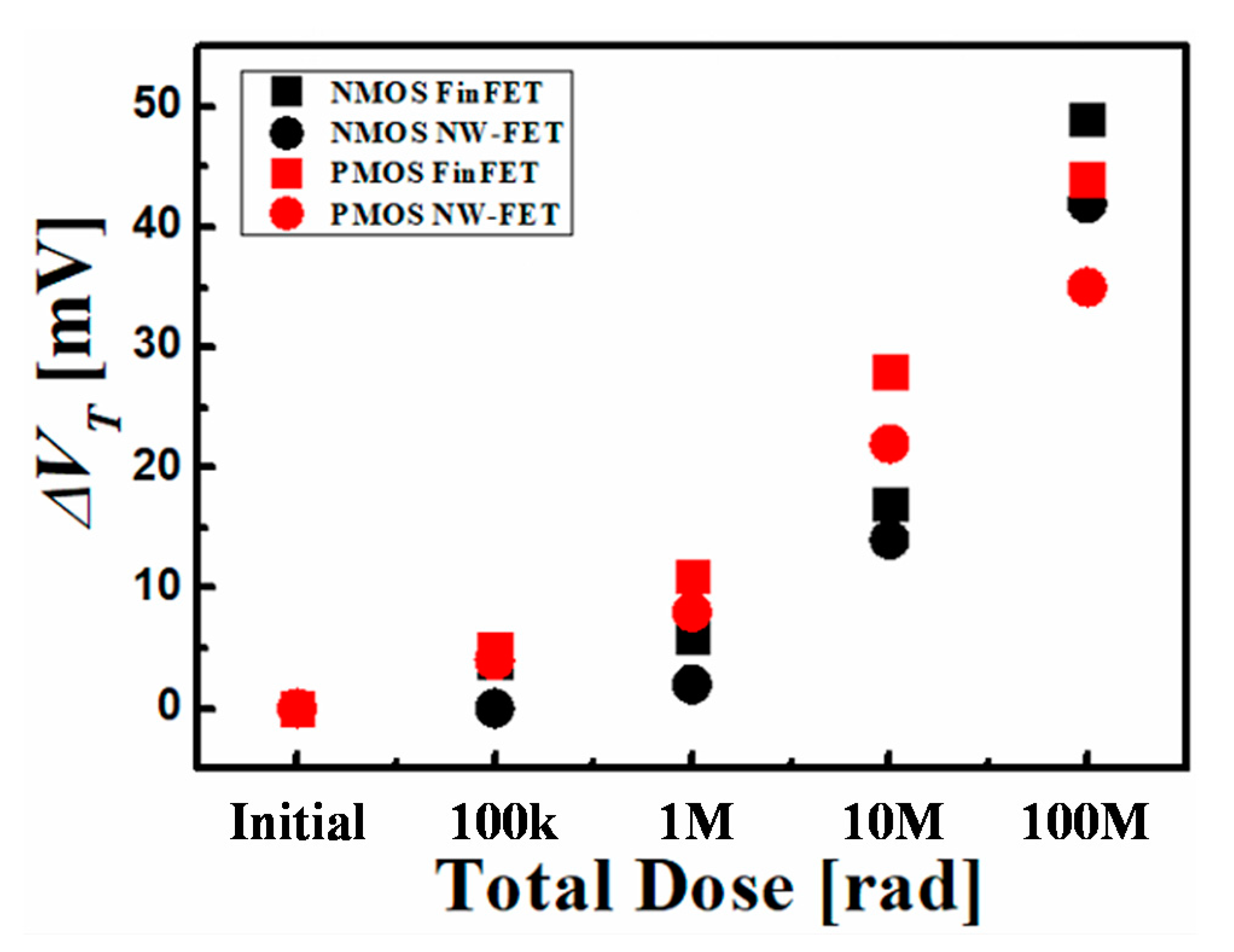
Figure 4.
Flow chart of the simulations considering the TID effect.

Figure 5.
Calibration of the electrical characteristics of the FinFET and NW-FET with the Berkeley short-channel insulated-gate FET (BSIM) common multi-gate (CMG) parameters.
Figure 5.
Calibration of the electrical characteristics of the FinFET and NW-FET with the Berkeley short-channel insulated-gate FET (BSIM) common multi-gate (CMG) parameters.
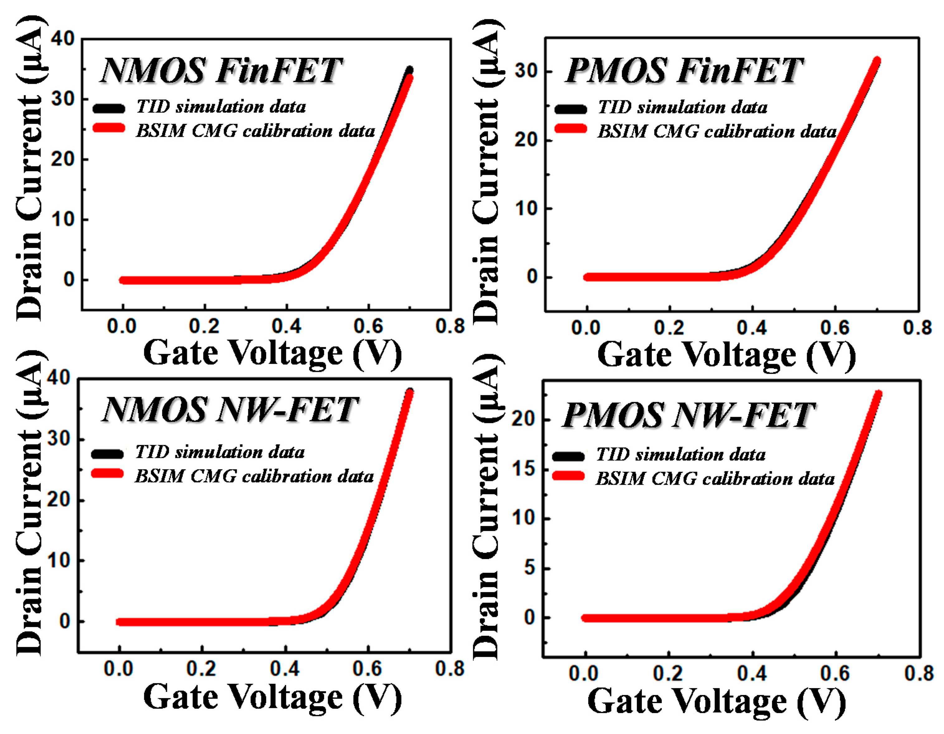
Figure 6.
FinFET and NW-FET inverter operation characteristics according to the accumulated radiation dose. (a,e) inverter input pulse; (b) FinFET inverter output for each total dose; (c) FinFET inverter operation of falling edge; (d) FinFET inverter operation of rising edge; (f) NW-FET inverter output for each total dose; (g) NW-FET inverter operation of falling edge; (h) NW-FET inverter operation of rising edge.

Table 1.
Device’s parameters.
| Design Factor | FinFET | NW-FET |
|---|---|---|
| Channel length | 12 nm | 12 nm |
| FinFET’s width and NW-FET’s diameter | 6 nm | 6 nm |
| Height (NW-FET total height) | 42 nm | 30 nm |
| Total area | 489.5 nm2 | 474.9 nm2 |
| S/D doping | 1 × 1021 cm−3 | 1 × 1021 cm−3 |
| Channel doping | 1 × 1016 cm−3 | 1 × 1016 cm−3 |
| Oxide area | 237.5 nm2 | 333.6 nm2 |
| EOT | 0.812 nm | 0.812 nm |
Table 2.
VT data of each device.
| VDD = 0.65 V | FinFET (VT) | NW-FET (VT) |
|---|---|---|
| NMOS | 0.33 V | 0.4 V |
| PMOS | 0.3 V | 0.38 V |
Publisher’s Note: MDPI stays neutral with regard to jurisdictional claims in published maps and institutional affiliations. |
© 2021 by the authors. Licensee MDPI, Basel, Switzerland. This article is an open access article distributed under the terms and conditions of the Creative Commons Attribution (CC BY) license (http://creativecommons.org/licenses/by/4.0/).
Share and Cite
MDPI and ACS Style
Won, H.; Kang, M. Analysis of Circuit Simulation Considering Total Ionizing Dose Effects on FinFET and Nanowire FET. Appl. Sci. 2021, 11, 894. https://doi.org/10.3390/app11030894
AMA Style
Won H, Kang M. Analysis of Circuit Simulation Considering Total Ionizing Dose Effects on FinFET and Nanowire FET. Applied Sciences. 2021; 11(3):894. https://doi.org/10.3390/app11030894
Chicago/Turabian StyleWon, Hyeonjae, and Myounggon Kang. 2021. "Analysis of Circuit Simulation Considering Total Ionizing Dose Effects on FinFET and Nanowire FET" Applied Sciences 11, no. 3: 894. https://doi.org/10.3390/app11030894
Note that from the first issue of 2016, this journal uses article numbers instead of page numbers. See further details here.