
In-Situ Photo-Dissociation and Polymerization of Carbon Disulfide with Vacuum Ultraviolet Microplasma Flat Lamp for Organic Thin Films


1
Laboratory of Optical Physics and Engineering, Department of Electrical and Computer Engineering, University of Illinois at Urbana-Champaign, Urbana, IL 61801, USA
2
Eden Park Illumination, Inc., Champaign, IL 61821, USA
*
Author to whom correspondence should be addressed.
Appl. Sci. 2021, 11(6), 2597; https://doi.org/10.3390/app11062597
Submission received: 18 February 2021
/
Revised: 10 March 2021
/
Accepted: 12 March 2021
/
Published: 15 March 2021
(This article belongs to the Section Applied Physics General)
Abstract
:Vacuum UV (VUV) photo-dissociation for a liquid phase organic compound, carbon disulfide (CS2), has been investigated. 172 nm (7.2 eV) VUV photons from Xe2* excimers in a microcavity plasma lamp irradiated free-standing liquid droplets on Si substrate in each a nitrogen environment and an atmospheric air environment. Selective and rapid dissociation of CS2 into C-C, C-S or C-O-S based fragments was observed in the different gas environments during the reaction. Thin-layered polymeric microdeposites have been identified by characterization with a Scanning electron microscope (SEM), Energy dispersive x-ray spectroscopy (EDX), Raman spectroscopy and X-ray photoelectron spectroscopy (XPS). This novel photo-process from the flat VUV microplasma lamp introduces another pathway of low-temperature organic (or synthetic) conversion for large area deposition. The in-situ, selective conversion of various organic precursors can be potentially used in optoelectronics and nanotechnology applications.
1. Introduction
Low temperature deposition techniques are becoming essential for many types of opto- and microelectronics fabricated in flexible substrates. Several approaches are currently being utilized to avoid damage on fragile substrates, such as plasma-enhanced chemical deposition (PECVD) and laser chemical deposition (LCVD) [1,2]. However, malleable substrates are subjected to high energetic ionic bombardment caused by plasma generation in the PECVD system, producing cracking and unwanted stoichiometry ratios in the deposited material [3,4,5]. In an LCVD system, lasers are costly and provide only a small area deposition about several cm2. Alternatively, an incoherent UV source can be used in many processing applications, since most organic/inorganic materials readily absorb photons in wavelengths < ~250 nm. However, the utilization of traditional UV sources (UVC) in chemical dissociation is still limited by insufficient photon energy associated with reactants’ chemical bonds, and ends in slow process rates (kinetics) unless it uses photo-catalysts. A new VUV (172 nm) flat lamp [6] has distinct benefits such as high radiation power, large and uniform area coverage that was not possible in the conventional photon sources for chemical reactions. In this research article, the experiment for dissociation of CS2 by a VUV lamp will be described in the different experimental conditions. As a conductive polymer, CS2 has been used as a sulfur dopant in organic chemistry and a solvent for various polymers [7,8]. In addition, CS2 can be used as an etchant of the carbon layer when it is used with plasma [9]. It has been known that CS2 can be readily dissociated to CS + S fragments through photons, catalytic reactions, and plasma processes in the vapor phases [10,11,12]. However, direct photodissociation of a free standing and volatile CS2 droplets on a substrate using high energy VUV photons (>7.2 eV) to deposit a thin layer that has never been explored. In addition, the conversion of the photo-fragments to a thin layer deposit in a scaled area of Si substrate is introduced. Being the first report of its kind for an in-situ high energy UV deposition methodology, the low temperature and simple deposition technology of organic precursors will lead to the cost-effectiveness of microelectronics processes.
2. Experimental Method
The operation principle of excimer lamps relies on the radiative decomposition of excimer dimers such as Xe2* (172 nm) formed in a plasma discharge of noble gases. As illustrated in Figure 1a, Xe2 is well known for emitting bright continua (150, 172 nm) along with resonance lines of Xe* (129 and 147 nm). The dominant Xe2 emission at 172 nm arises from A1 → X1 transitions of the molecule and its emission intensities’ growth are attributed to the three-body collision of excited state Xe* and 2Xe ground state atoms [6]. The formation rate of these three body reactions is increased quadratically with Xe gas pressure. The structure of the microplasma lamp used here has an array of microcavities that produces a low temperature and non-equilibrium plasmas. The electron temperature of microplasma lies in the 2–5 eV interval, which is ideal for forming the excimer (Xe2) and increasing its transition intensities. Another advantage of using excimer lamps is that the non-stable ground state of an excimer lamp is able to have no self-absorption of the emitted illumination, providing a high UV intensity. In addition, the flat form factor and diffusive glow in the lamp make a uniform treatment over the area of the lamp. Therefore, the deposition area can be easily scaled along with the flat lamp size at given intensities.
Figure 2a demonstrates the operation of the 172 nm microplasma VUV lamp (100 × 100 mm, Eden Park Illumination, Inc. Champaign, IL, USA). The lamp is filled with 500 Torr of 70% Xe/Ne gas mixture, and operated at 20–30 kHz of 3 kV pulses. The output intensity at the surface of the lamp was 17 mW/cm2. Figure 2b shows the VUV emission spectrum from the lamp. Figure 1b is a schematic of the potential energy curves in the excited states of CS2 [13]. The red dashed line corresponds to the 172 nm VUV lamp photon energy (7.2 eV) in this experiment. Photon energy from the VUV lamp sufficiently covers the energies required to dissociate the C=S bond of the CS2. The configuration of the VUV photodissociation setup were shown in Figure 2c. The distance between the VUV lamp and substrate was maintained 1 cm. VUV photons are affected by environmental conditions as it is readily absorbed by surrounded chemical species such as water vapor or oxygens. It means that VUV photons cannot travel long distances. The experiment has been performed in the N2 (purged) environment, which does not absorb the 7.2 eV photons, to minimize the photon losses (and observe the contribution of VUV photons to the overall reaction). Besides, we also performed the experiments at ambient (dry air) environment preferring the formation of active oxygen species by moisture and oxygen. The latter condition led to the deposition of a series of compounds (associated with oxidation, as shown in results from EDS). The distance of 1 cm was chosen from the multiple tests to find the optimal distance, which maintains the consistency between two experimental approaches and keeping a balance between photochemistry and direct photo-radiation. A shorter distance than 1 cm was not considered in these experiments to avoid any interaction between the target substrates (or chemical vapors) and the flat lamp itself. Free-standing, liquid phase CS2 droplets (99.99%, Sigma-Aldrich, St. Louis, MO, USA) were applied to the Si substrate with a micropipette for quantitative sampling from 0.2 mL to 3 mL. The chamber was purged with an atmospheric pressure of either research-grade N2 or dry air with a flow rate of 5 slm. After VUV irradiation to the target substrate, the treated samples were analyzed by SEM (4700 Hitachi), EDX (iXRF Oxford Instruments), Raman spectroscopy (Raman 11, Nanophoton), and XPS (Axis ULTRA, Kratos) to investigate the chemical composition and morphology of the deposited films.
3. Discussion
The photo-dissociation of free-standing CS2 liquid samples were performed as a function of time and different sample volumes. The immediate photo-dissociation and a deposit formation were observed within one minute of VUV irradiation. After 3 min, most liquid phase samples disappear due to photo-dissociation or vaporization of the original compound. Figure 3 shows the SEM images of microdeposits formed on the Si substrate after 3 min of VUV irradiation in various CS2 sample volumes. The deposited area in each sample is proportional to the quantitative volumes of CS2. The darker area is a deposited area from the CS2 precursor decomposition, and lighter areas indicate the Si substrate. When the CS2 precursor is applied to the Si substrate, it immediately evaporates without leaving any residues. However, the 172 nm photons convert the free standing precursors into different morphology films in either N2 or air environment, covering the entire Si substrate.
The VUV photons also make a selective reaction pathway to a specific product by the modification of reaction parameters during the process. The initial process condition of an N2 environment was chosen to form an inert condition because N2 does not react with VUV. It also helps VUV photons travel to the target substrate without any absorption from environmental contaminants. On the other hand, the ambient O2 gas efficiently absorbs the VUV photons to form an oxygen atom species (O) or ozone (O3). These new species can modify the existing reaction mechanism of the CS2 dissociation process and create alternative synthetic pathways. The experiments under the air environment were made to compare the photochemistry of N2. Samples from air environment yielded a different morphology than was obtained from the N2 environment. The formation rate in air was close to the rate in the N2 environment. Figure 4 shows the results of EDX analysis for deposit samples on the Si substrate, and the table provides the information of a possible composition of identified components in the deposited layer. For the test samples obtained in the N2 environment (Figure 4a), the atomic percentages of carbon (C) and sulfur (S) exhibit 15.7% and 0.35%, respectively. Only a negligible content of S element was observed in the layer. It strongly indicates that high energy photons of the microplasma lamp effectively dissociates the C=S bond of CS2 and creates a deposit with carbon-rich composites (with a possible base-bonding unit of C-C and/or C-S-C). By switching the gas environment from N2 to air in Figure 4b, the atomic percentages of C, S, and O were 20.37%, 1.49%, and 1.5%, respectively. As is discussed previously, strong co-absorption of O2 for VUV photons results in the participation of oxygen species in the chemical reactions. The most probable product from this oxidative process is the formation of O-C-S-based compounds, and it is a standard component identified in other oxidation processes of CS2 [14,15]. It should be also noted that the atomic percentage ratio of each elements is considered as a relative proportional values because of the involvement of Si wafer (substrate) as a primary elementsl in the EDS analysis.
Figure 5 shows the Raman spectroscopy for the deposit compounds as well as the spectrum from the Si substrate as a reference. CS2 is a strong Raman scatter due to its symmetric chemical structure and vibration modes. The comparison of vibrational modes in the Raman spectra between the CS2 driven products is straightforward [16,17]. In the spectra of two deposit samples, any vibrations of CS2 molecule (typically at 656 and 800 cm−1) were identified, indicating that the CS2 was fully decomposed by VUV irradiation. Each deposit formed at N2 or air environment does not show any similarities in the spectra. Both Raman spectra in Figure 5a,b show a broad baseline band in the range of 1800–3500 cm−1, which was not found in either CS2 or Si substrate, and shows the characteristic of a polymeric layer or multi-element composites. Among them, the continuum peak in the range of 2300 cm−1 to 2700 cm−1 and another peak at 2883 cm−1 are related to the carbon related vibrations and CH stretching vibration of the deposited films, respectively [18,19,20,21]. In these cases, the existence of such a broad peak in the Raman spectra could be assumably attributed to a morphology of the polymenric layer or electronic Raman scattering [22]. The peak at 3390 cm−1 indicate the synthesis of the amorphous status of carbon. The broad ones at 1550 cm−1 correspond to C-O vibrations [23]. The sharp transition at ~2336 cm−1 arises from ambient nitrogen (molecular) gas (Q-branch) [24,25] and the peak at 1586 cm−1 is assigned as ambient O2 scattering. Both peaks are found due to the atomospheric scattering by the collimated probing laser beam at the substrate, as notated in Figure 5c [26].
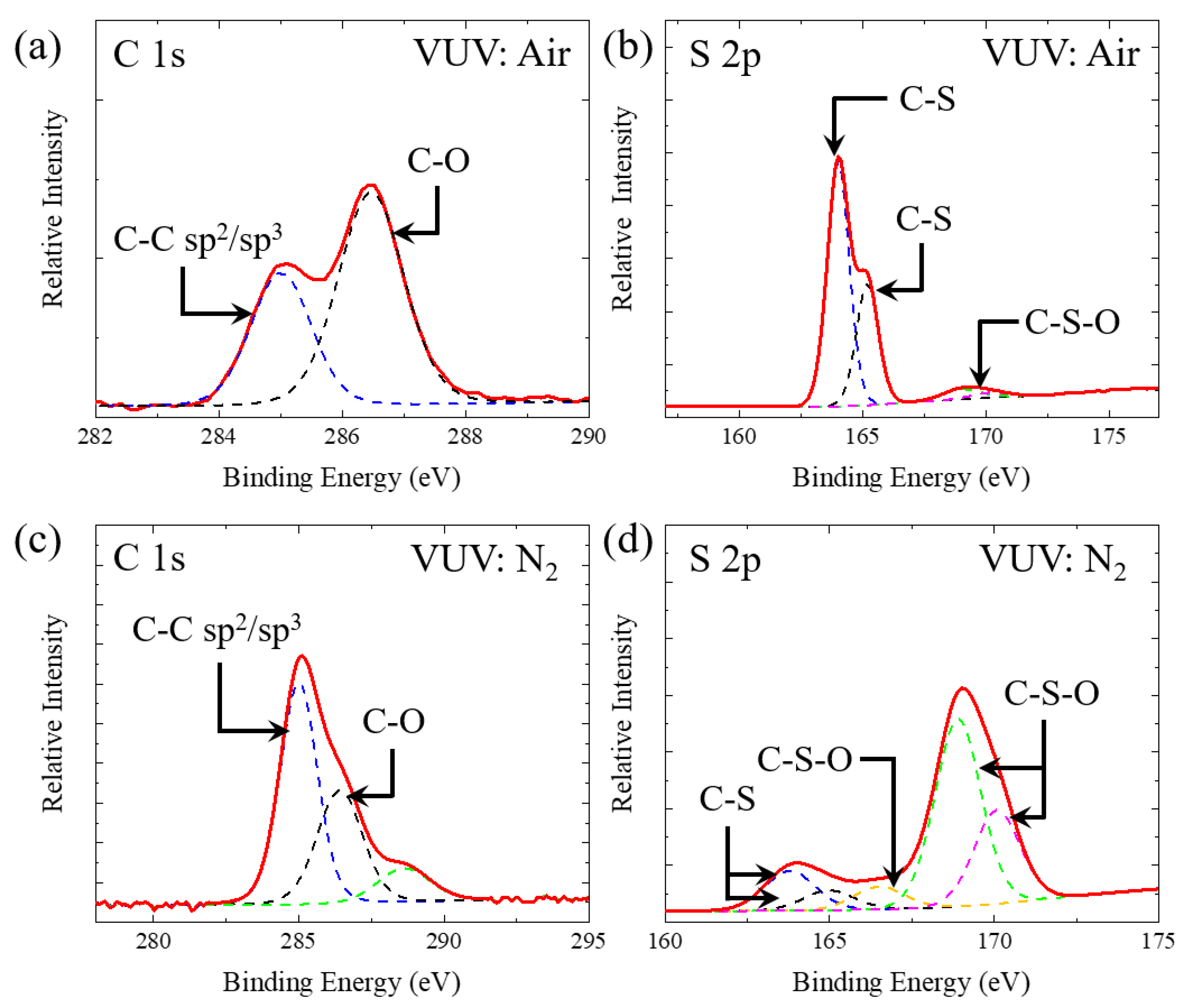
The chemical bondings formed in the deposited films after VUV irradiation were investigated by XPS. Representative C 1s and S 2p XPS spectra of a deposited film including deconvoluated peak assignments are illustrated in Figure 6. Figure 6a,b show the C 1s and S 2p core level spectra of the sample after VUV irradiation with air environment, respectively. The deconvoluation of C 1s spectrum is composed of two curves which correspond to the carbon bonding (sp3) and C-O bonding [27,28,29,30]. S 2p peak can be deconvoluted into three species, corresponding to the C-S and S-O bond [30,31,32]. As shown in Figure 6c, the 288 eV component is tentatively assigned to amide C (N-C=O), carboxyl C (O-C=O) and carbonyl C (C=O) [30,33]. While XPS measurements of samples with VUV irradiation in N2 environment shows completely different spectra in Figure 6c,d. The spectrum of sp3 C shows relatively higher intensity than C-O bond in Figure 6c which was the opposite to the spectrum shown in Figure 6a. This is because larger fluence of VUV photons from the microplasma lamp reached to CS2 precursor in N2 environment, resulting in a higher C-C bond than C-O bond spectra. However, the high absorption of VUV photons by oxygen in the air environment will prevent delivering photons to the substrate than in the N2 environment. Therefore, we expect that O3 or active oxygen species will involve more than VUV photons in this specific process, which resulted in a higher C-O bond than C-C bond spectra in Figure 6a. Besides, the intensity of C-S peaks in air (Figure 6b) was higher than that of Figure 6d by the factor of 10. It shows that the VUV photodissociation of C=S (in CS2) leads the reaction pathways preferably toward C-C polymerization after the complete dissociation of C=S double bonds rather than forming C-S bond based polymeric bonds. The C-S-O bond formation is related to the partial oxidation with the C-S fragments, mainly obtained by direct photodissociation of a C=S bond of CS2 [10]. In the air environment (Figure 6a,b), the formation of the C-O component is preferred over than C-S-O formation due to the oxidative dissociation process of C=S bonds as described above. The results indicate the strong possibility of designed manipulation of different reaction (deposition) pathways through the different controlled conditions (such as environment, photon fluence, or time). In particular, all the parameters in this low-temperature photochemistry can be precisely (and simply) controlled compared to the conventional reaction parameters.
4. Conclusions
This study describes in-situ, low temperature, photo-assisted dissociation of CS2 on a Si substrate with a VUV (172 nm) microplasma lamp with a flat form factor. Xe2 excimer VUV sources deliver sufficient photon energy of 7.2 eV to the organic reactant to dissociate its C=S bonding at a higher reaction rate within a few minutes. The analysis of the deposited product indicates the possibility of the formation of either a C-C or C-S based polymeric deposit on the substrate. Especially, the investigation of the thin layers by Raman spectroscopy and X-ray photoelectron scpectroscpy indicates that the resulting carbon bond was initiated from the CS2 dissociaiton, and it coincides with other reaction mechanisms of the conventional plasma enhanced or photochemical vapor deposition. We have also found that chemical bond and composition could be changed depending on the efficiency of VUV photon delivery, mainly dependent on the controlled environment. It has been known that the material backbones are closely related to the electrical properties of either semiconductors or conductors, depending on its thin-film structure. Amorphous deposits were also identified in the characterization, and selective formation of the different products was also observed in different environmental parameters associated with VUV absorption. It has the potential to be an efficient technique for in-situ deposition thanks to its simple controllability of deposition parameters and scalable deposition area. Furthermore, the use of other VUV wavelengths from the microplasma lamps (especially for having its photo-energy higher than 7.2 eV) in the microplasma lamp will open a novel photochemical tool for the conversion of various organic/inorganic precursors. At present, the 7.2 eV photons efficiently dissociate (initiate the photochemistry) precursor materials containing any chemical double bond structures according to the preliminary studies for the various materials. It is expected that higher photon energies (>8.7 eV) would achieve the photodissociation of, for example, carbon triple bonds in the controlled environment. The VUV-assisted dissociation mechanism at 300 K appears to be very attractive for industrial applications in electronic and optical device manufacturing. It is also applicable for environmental applications such as the remediation of harmful organic compounds in the air [15,34].
Author Contributions
Conceptualization, J.K. and S.-J.P.; methodology, J.K. and S.-J.P.; validation, J.K. and S.-J.P.; investigation, J.K. and S.-J.P.; data curation, J.K. and S.-J.P.; writing—original draft preparation, J.K; writing—review and editing, S.-J.P.; supervision, S.-J.P.; project administration, S.-J.P.; funding acquisition, S.-J.P. All authors have read and agreed to the published version of the manuscript.
Funding
This research was funded by the Ministry of Environment, Republic of Korea (MOE).
Institutional Review Board Statement
Not applicable.
Informed Consent Statement
Not applicable.
Data Availability Statement
Not applicable.
Acknowledgments
This research was supported by R&D Center for Green Patrol Technologies through the R&D for Global Top Environmental Technologies funded by the Ministry of Environment, Republic of Korea (MOE).
Conflicts of Interest
The authors declare no conflict of interest.
References
- Vasudev, M.C.; Anderson, K.D.; Bunning, T.J.; Tsukruk, V.V.; Naik, R.R. Exploration of Plasma-Enhanced Chemical Vapor Deposition as a Method for Thin-Film Fabrication with Biological Applications. ACS Appl. Mater. Interfaces 2013, 5, 3983–3994. [Google Scholar] [CrossRef]
- Duty, C.; Jean, D.; Lackey, W. Laser chemical vapour deposition: Materials, modelling, and process control. Int. Mater. Rev. 2001, 46, 271–287. [Google Scholar] [CrossRef]
- Kow-Ming, C.; Wen-Chih, Y.; Chiu-Pao, T. Performance and reliability of low-temperature polysilicon TFT with a novel stack gate dielectric and stack optimization using PECVD nitrous oxide plasma. IEEE Trans. Electron Devices 2004, 51, 63–67. [Google Scholar]
- Fritz, A.K.; Olmer, L.J. Detecting and Preventing Gate Oxide Plasma Damage During PECVD Carbon Deposition Through Surface Photovoltage Measurements. IEEE Trans. Semicond. Manuf. 2017, 30, 426–433. [Google Scholar] [CrossRef]
- Zhiwei, X.; Christopher, B.; Maggie, L.; Chris, N. Plasma damage monitoring for PECVD deposition: A contact potential difference study and device yield analysis. In Proceedings of SPIE; Ajuria, S.A., Hossain, T.Z., Eds.; SPIE: Washington, DC, USA, 1998; Volume 3509. [Google Scholar]
- Park, S.-J.; Herring, C.M.; Mironov, A.E.; Cho, J.H.; Eden, J.G. 25 W of average power at 172 nm in the vacuum ultraviolet from flat, efficient lamps driven by interlaced arrays of microcavity plasmas. APL Photonics 2017, 2, 041302. [Google Scholar] [CrossRef] [Green Version]
- Ochiai, B.; Endo, T. Carbon dioxide and carbon disulfide as resources for functional polymers. Prog. Polym. Sci. 2005, 30, 183–215. [Google Scholar] [CrossRef]
- Kudryashov, S.I.; Nguyen, L.V.; Kirilenko, D.A.; Brunkov, P.N.; Rudenko, A.A.; Busleev, N.I.; Shakhmin, A.L.; Semencha, A.V.; Khmelnitsky, R.A.; Melnik, N.N.; et al. Large-Scale Laser Fabrication of Antifouling Silicon-Surface Nanosheet Arrays via Nanoplasmonic Ablative Self-Organization in Liquid CS2 Tracked by a Sulfur Dopant. ACS Appl. Nano Mater. 2018, 1, 2461–2468. [Google Scholar] [CrossRef]
- Kim, J.K.; Cho, S.I.; Kim, N.G.; Jhon, M.S.; Min, K.S.; Kim, C.K.; Yeom, G.Y. Study on the etching characteristics of amorphous carbon layer in oxygen plasma with carbonyl sulfide. J. Vac. Sci. Technol. A 2013, 31, 021301. [Google Scholar] [CrossRef] [Green Version]
- Colman, J.J.; Trogler, W.C. Photopolymerization of Carbon Disulfide Yields the High-Pressure-Phase (CS2)x. J. Am. Chem. Soc. 1995, 117, 11270–11277. [Google Scholar] [CrossRef]
- Heymann, D.; Cataldo, F.; Thiemens, M.H.; Fokkens, R.; Nibbering, N.M.M.; Vis, R.D. Formation of CmSn compounds by photopolymerization of CS2 in the atmosphere of Jupiter. Meteorit. Planet. Sci. 2000, 35, 355–361. [Google Scholar] [CrossRef]
- TAnderson, S.; Ma, J.H.; Park, S.; Eden, J.G. Multichannel Microchemical Reactor Comprising Replica-Molded Microplasma Devices: Chemiluminescence and Sulfur Deposition in Ar/CS2 Flows. IEEE Trans. Plasma Sci. 2008, 36, 1250–1251. [Google Scholar] [CrossRef]
- Horio, T.; Spesyvtsev, R.; Furumido, Y.; Suzuki, T. Real-time detection of S(1D2) photofragments produced from the 1B2(1Σu+) state of CS2 by vacuum ultraviolet photoelectron imaging using 133 nm probe pulses. J. Chem. Phys. 2017, 147, 013932. [Google Scholar] [CrossRef] [Green Version]
- Heicklen, J.; Olszyna, K.J. Reaction of ozone with carbon disulfide. J. Phys. Chem. 1970, 74, 4188–4198. [Google Scholar] [CrossRef]
- Yan, X.; Sun, Y.; Zhu, T.; Fan, X. Conversion of carbon disulfide in air by non-thermal plasma. J. Hazard. Mater. 2013, 261, 669–674. [Google Scholar] [CrossRef] [PubMed]
- Ito, M. Raman and Infrared Spectra of Crystalline Carbon Disulfide. J. Chem. Phys. 1965, 42, 815. [Google Scholar] [CrossRef]
- Wang, D.; Mittauer, K.; Reynolds, N. Raman scattering of carbon disulfide: The temperature effect. Am. J. Phys. 2009, 77, 1130–1134. [Google Scholar] [CrossRef]
- Hoffmann, G.G.G.; De With, G.; Loos, J.J. Micro-Raman and Tip-Enhanced Raman Spectroscopy of Carbon Allotropes. Macromol. Symp. 2008, 265, 1–11. [Google Scholar] [CrossRef]
- Miranda, A.M.; Castilho-Almeida, E.W.; Ferreira, E.H.M.; Moreira, G.F.; Achete, C.A.; Armond, R.A.; Dos Santos, H.F.; Jorio, A. Line shape analysis of the Raman spectra from pure and mixed biofuels esters compounds. Fuel 2014, 115, 118–125. [Google Scholar] [CrossRef] [Green Version]
- Bock, P.; Gierlinger, N. Infrared and Raman spectra of lignin substructures: Coniferyl alcohol, abietin, and coniferyl aldehyde. J. Raman Spectrosc. 2019, 50, 778–792. [Google Scholar] [CrossRef] [PubMed]
- Howell, N.K.; Arteaga, G.; Nakai, S.; Li-Chan, E.C.Y. Raman Spectral Analysis in the C−H Stretching Region of Proteins and Amino Acids for Investigation of Hydrophobic Interactions. J. Agric. Food Chem. 1999, 47, 924–933. [Google Scholar] [CrossRef] [PubMed]
- Popović, D.M.; Milosavljević, V.; Žekić, A.; Romčević, N.; Daniels, S. Raman scattering analysis of silicon dioxide single crystal treated by direct current plasma discharge. Appl. Phys. Lett. 2011, 98, 051503. [Google Scholar] [CrossRef] [Green Version]
- Mukherjee, P.K.; Roy, M.; Mandal, B.P.; Dey, G.K.; Ghatak, J.; Tyagi, A.K.; Kale, S.P. Green synthesis of highly stabilized nanocrystalline silver particles by a non-pathogenic and agriculturally important fungus T. asperellum. Nanotechnology 2008, 19, 075103. [Google Scholar] [CrossRef]
- Spizzirri, P.; Fang, J.; Rubanov, S.; Gauja, E.; Prawer, S. Nano-Raman spectroscopy of silicon surfaces. arXiv 2010, arXiv:1002.2692. [Google Scholar]
- Hyatt, H.A.; Cherlow, J.M.; Fenner, W.R.; Porto, S.P.S. Cross section for the Raman effect in molecular nitrogen gas. J. Opt. Soc. Am. 1973, 63, 1604–1606. [Google Scholar] [CrossRef]
- Odhner, J.H.; Romanov, D.A.; Levis, R.J. Filament-based stimulated Raman spectroscopy. In Proceedings of the SPIE LASE, San Francisco, CA, USA, 17 February 2010; SPIE—International Society for Optical Engineering: Washington, DC, USA, 2010; p. 75820M. [Google Scholar]
- Dwivedi, N.; Yeo, R.J.; Satyanarayana, N.; Kundu, S.; Tripathy, S.; Bhatia, C.S. Understanding the Role of Nitrogen in Plasma-Assisted Surface Modification of Magnetic Recording Media with and without Ultrathin Carbon Overcoats. Sci. Rep. 2015, 5, 7772. [Google Scholar] [CrossRef] [Green Version]
- Pathem, B.K.; Guo, X.-C.; Rose, F.; Wang, N.; Komvopoulos, K.; Schreck, E.; Marchon, B. Carbon Overcoat Oxidation in Heat-Assisted Magnetic Recording. IEEE Trans. Magn. 2013, 49, 3721–3724. [Google Scholar] [CrossRef]
- Goohpattader, P.S.; Dwivedi, N.; Rismani-Yazdi, E.; Satyanarayana, N.; Yeo, R.J.; Kundu, S.; Bhatia, C. Probing the role of C+ ion energy, thickness and graded structure on the functional and microstructural characteristics of ultrathin carbon films (<2 nm). Tribol. Int. 2015, 81, 73–88. [Google Scholar]
- Sun, D.; Ban, R.; Zhang, P.-H.; Wu, G.-H.; Zhang, J.-R.; Zhu, J.-J. Hair fiber as a precursor for synthesizing of sulfur- and nitrogen-co-doped carbon dots with tunable luminescence properties. Carbon 2013, 64, 424–434. [Google Scholar] [CrossRef]
- Ye, J.; He, F.; Nie, J.; Cao, Y.; Yang, H.; Ai, X. Sulfur/carbon nanocomposite-filled polyacrylonitrile nanofibers as a long life and high capacity cathode for lithium–sulfur batteries. J. Mater. Chem. A 2015, 3, 7406–7412. [Google Scholar] [CrossRef]
- Wang, X.; Gao, T.; Han, F.; Ma, Z.; Zhang, Z.; Li, J.; Wang, C. Stabilizing high sulfur loading Li–S batteries by chemisorption of polysulfide on three-dimensional current collector. Nano Energy 2016, 30, 700–708. [Google Scholar] [CrossRef] [Green Version]
- Gerin, P.; Dengis, P.; Rouxhet, P. Performance of XPS analysis of model biochemical compounds. J. Chim. Phys. 1995, 92, 1043–1065. [Google Scholar] [CrossRef]
- Rich, A.L.; Patel, J.T. Carbon Disulfide (CS2) Mechanisms in Formation of Atmospheric Carbon Dioxide (CO2) Formation from Unconventional Shale Gas Extraction and Processing Operations and Global Climate Change. Environ. Health Insights 2015, 9, EHI.S15667. [Google Scholar] [CrossRef] [PubMed]
Figure 1.
(a) Basic energy and transition diagram of VUV emission of Xe2 excimer lamp, (b) Schematic potential energy curve of the target molecule, CS2 with 172 nm VUV lamp energy level (red dash line).
Figure 1.
(a) Basic energy and transition diagram of VUV emission of Xe2 excimer lamp, (b) Schematic potential energy curve of the target molecule, CS2 with 172 nm VUV lamp energy level (red dash line).

Figure 2.
(a) Photographs of microplasma VUV lamp operation and an expanded view of a lamp surface, (b) VUV emission spectrum of the lamp, (c) Schematic of CS2 synthesis from VUV lamp illumination.
Figure 2.
(a) Photographs of microplasma VUV lamp operation and an expanded view of a lamp surface, (b) VUV emission spectrum of the lamp, (c) Schematic of CS2 synthesis from VUV lamp illumination.
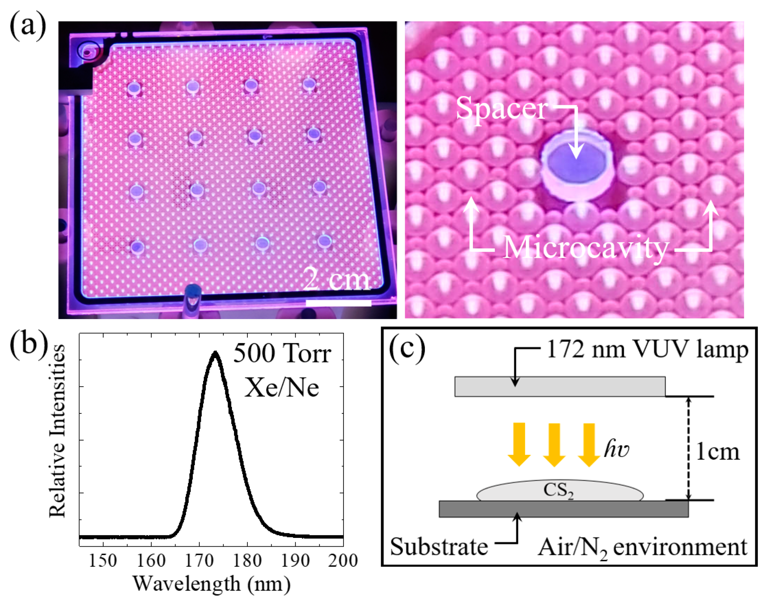
Figure 3.
SEM images of microdeposits formed on a Si substrate during the irradiation of 172 nm VUV photons for 3 min. The different amounts of precursors are irradiated: (a) 0.2 mL, (b) 0.5 mL, (c) 1 mL, (d) 3 mL of CS2 under nitrogen environment at 300 K.
Figure 3.
SEM images of microdeposits formed on a Si substrate during the irradiation of 172 nm VUV photons for 3 min. The different amounts of precursors are irradiated: (a) 0.2 mL, (b) 0.5 mL, (c) 1 mL, (d) 3 mL of CS2 under nitrogen environment at 300 K.
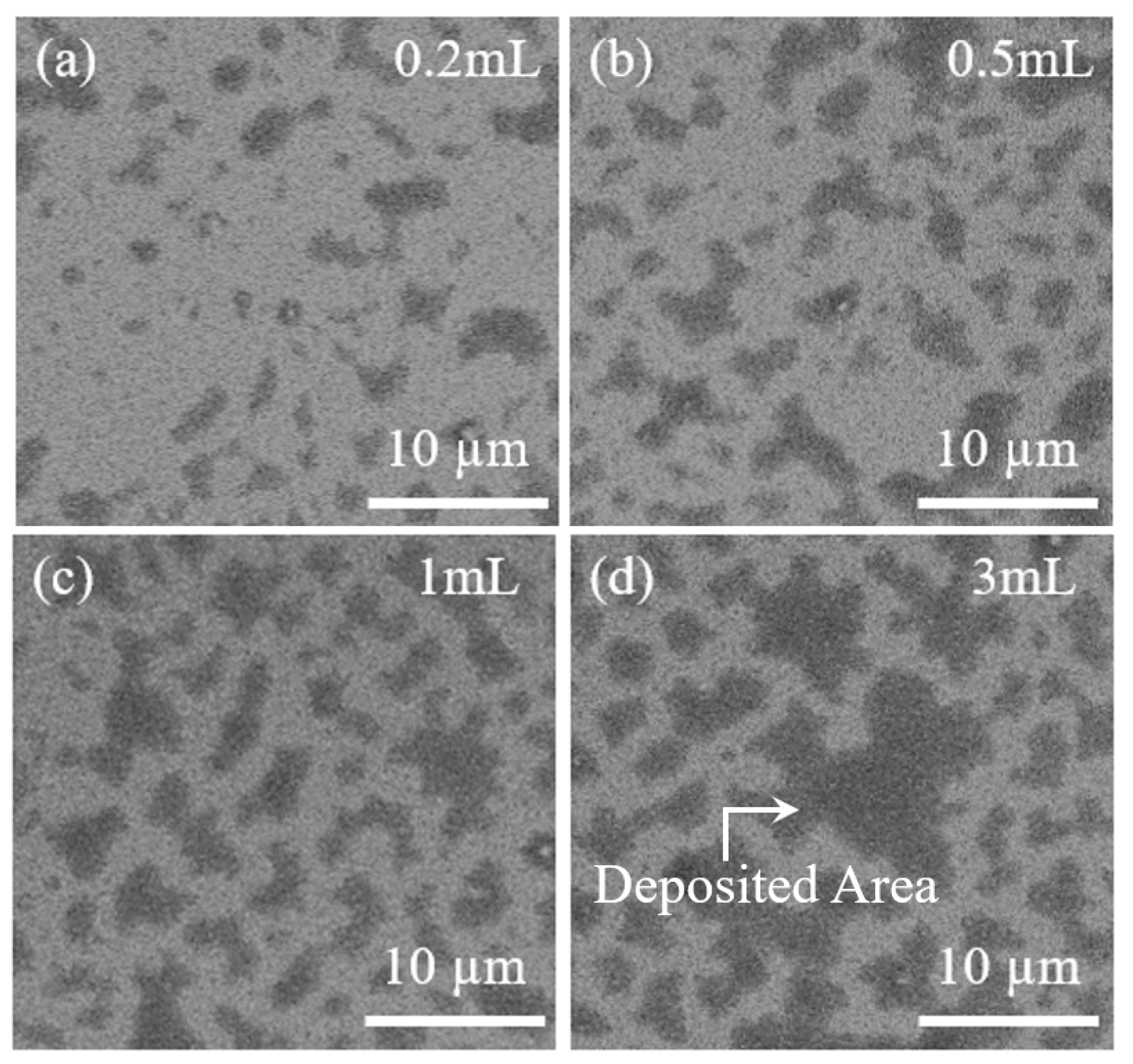
Figure 4.
EDS analysis for the deposited layers. The numerical analysis results are listed at tables: (a) VUV photo-dissociation in N2, (b) in atmospheric air. The white square marks (in the left hand side images) in the SEM microscope images indicate the analysis area in the sample.
Figure 4.
EDS analysis for the deposited layers. The numerical analysis results are listed at tables: (a) VUV photo-dissociation in N2, (b) in atmospheric air. The white square marks (in the left hand side images) in the SEM microscope images indicate the analysis area in the sample.
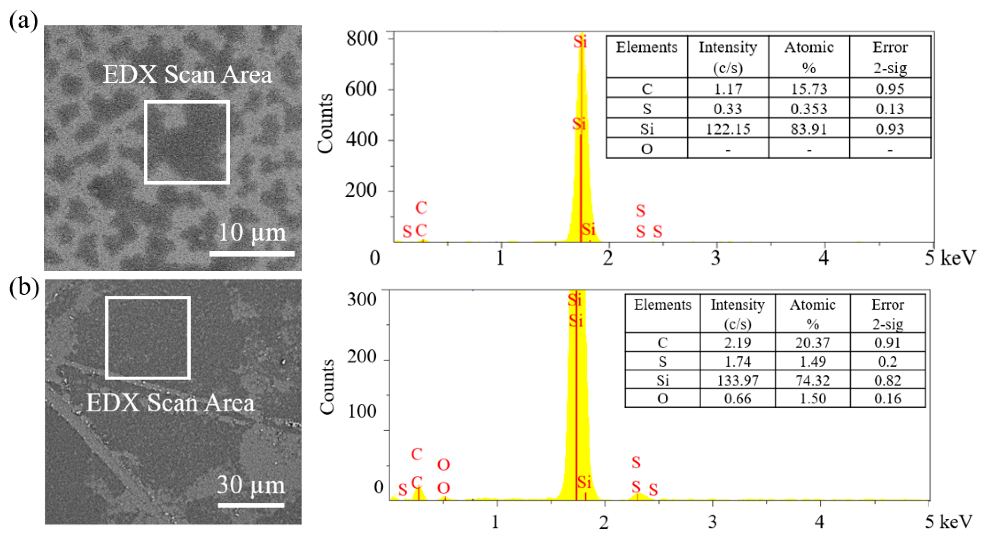
Figure 5.
Raman spectrum analysis of the micro-deposit on a Si substrate formed by VUV illumination under (a) N2 environment (b) atmospheric air, (c) Si substrate (for comparison), respectively.
Figure 5.
Raman spectrum analysis of the micro-deposit on a Si substrate formed by VUV illumination under (a) N2 environment (b) atmospheric air, (c) Si substrate (for comparison), respectively.
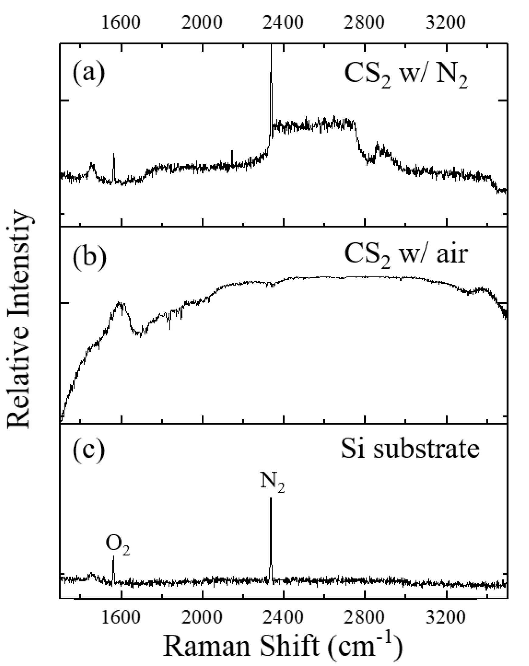
Figure 6.
XPS spectra of the C 1s and S 2p chemical states in the CS2 VUV assisted dissociation film with air (a,b) and nitrogen (c,d) environment at 300 K on Si substrate.
Figure 6.
XPS spectra of the C 1s and S 2p chemical states in the CS2 VUV assisted dissociation film with air (a,b) and nitrogen (c,d) environment at 300 K on Si substrate.
Publisher’s Note: MDPI stays neutral with regard to jurisdictional claims in published maps and institutional affiliations. |
© 2021 by the authors. Licensee MDPI, Basel, Switzerland. This article is an open access article distributed under the terms and conditions of the Creative Commons Attribution (CC BY) license (http://creativecommons.org/licenses/by/4.0/).
Share and Cite
MDPI and ACS Style
Kim, J.; Park, S.-J. In-Situ Photo-Dissociation and Polymerization of Carbon Disulfide with Vacuum Ultraviolet Microplasma Flat Lamp for Organic Thin Films. Appl. Sci. 2021, 11, 2597. https://doi.org/10.3390/app11062597
AMA Style
Kim J, Park S-J. In-Situ Photo-Dissociation and Polymerization of Carbon Disulfide with Vacuum Ultraviolet Microplasma Flat Lamp for Organic Thin Films. Applied Sciences. 2021; 11(6):2597. https://doi.org/10.3390/app11062597
Chicago/Turabian StyleKim, Jinhong, and Sung-Jin Park. 2021. "In-Situ Photo-Dissociation and Polymerization of Carbon Disulfide with Vacuum Ultraviolet Microplasma Flat Lamp for Organic Thin Films" Applied Sciences 11, no. 6: 2597. https://doi.org/10.3390/app11062597
Note that from the first issue of 2016, this journal uses article numbers instead of page numbers. See further details here.