
Analysis of Ruggedness of 4H-SiC Power MOSFETs with Various Doping Parameters


Department of Electrical Engineering, Pusan National University, Busan 46241, Republic of Korea
*
Author to whom correspondence should be addressed.
Appl. Sci. 2023, 13(1), 427; https://doi.org/10.3390/app13010427
Submission received: 8 December 2022
/
Revised: 26 December 2022
/
Accepted: 26 December 2022
/
Published: 29 December 2022
(This article belongs to the Special Issue Device Modeling for TCAD and Circuit Simulation)
Abstract
:This work investigates the effect of the doping concentration of SiC power metal-oxide–semiconductor field-effect transistors (MOSFETs) under an unclamped inductive switching (UIS) condition. Switching circuits such as inverters and motor-drive circuits often face unexpected operating conditions; therefore, a UIS test is performed to assess the avalanche ruggedness of the device, and design parameters such as the doping concentration should be considered to improve the UIS characteristics. Technology computer-aided design circuit simulation results, such as the current flows during failure and electrical changes, were obtained by changing the doping concentration of each region in the SiC power MOSFET.
1. Introduction
SiC power metal-oxide–semiconductor field-effect transistors (MOSFETs), which have the advantages of a higher thermal conductivity, smaller device size, lower power dissipation, and faster switching speed than Si devices, are widely used in power applications. However, switching circuits such as traction inverters may lead to device instability and an abnormal operation when a circuit operates in the high-power condition for a long time. Additionally, device structural parameters such as the p-base, N+ source, and P+ source doping can influence the device robustness under unexpected operating conditions such as with unclamped inductive switching (UIS). It is, therefore, necessary to evaluate their ruggedness and to understand their failure mechanisms under abnormal operating conditions. In this work, their characteristics are analyzed through technology computer-aided design (TCAD) circuit simulations. By varying the doping concentration of the p-base, N+ source, and P+ source regions, the ruggedness of the device under the avalanche mode can be improved [1,2,3,4,5,6,7,8,9].
2. Materials and Methods
2.1. Unclamped Inductive Switching (UIS) Circuit Test
Figure 1 illustrates the unclamped inductive switching (UIS) test circuit. This circuit was used to assess the avalanche ruggedness of the device. As shown in Figure 2a, when the device under test (DUT) was turned on by a single gate pulse (), the inductor current gradually increased, and the device temperature rose by joule-heating during a , as shown in Figure 2b. When the DUT turned off, the power MOSFET entered the avalanche mode in which the increased to a value close to the breakdown voltage, and the current flowed to the load devices to eliminate the inductor current. However, there was no load device in the UIS circuit and the inductor current was entirely terminated in the DUT. The electrons remaining in the p-base and the holes, which were the majority of carriers in the p-base region, underwent a recombination, and the current was gradually decreased. The blocking voltage increased until the recombination was completed, as shown in Figure 2c [10].
2.2. Device Failure Mechanisms
The Si power MOSFET failed when the parasitic bipolar junction transistor (BJT) was activated. The body diode and the parasitic BJT are shown in Figure 3. The voltage drop between the base-emitter () for the parasitic Si NPN BJT was approximately 0.7 V. When the temperature increased, the decreased gradually until the parasitic BJT was activated [11]; however, the for the parasitic SiC NPN BJT was approximately 2–3 V, and the BJT activation due to the temperature increasing was not a main reason for the device failure. As discussed in Section 2.1, when the DUT was turned-off, the blocking voltage increased until the recombination was completed; however, if the DUT had been turned on for a longer time, too many electrons could have remained in the p-base region. Then, the avalanche breakdown that caused the failure of the DUT may have occurred before the electrons remaining in the p-base region were completely recombinated with the holes. As shown in Figure 4a, the inductor current increased when the DUT failed, and the went to zero. Additionally, the temperature of the device increased, as shown in Figure 4b [12,13].
2.3. Device Description
Figure 3 illustrates the structure of a 1.7 kV 4H-SiC MOSFET. The MOSFET was designed using the Sentaurus TCAD simulation tool. The drift-layer doping concentration () and drift thickness () for a breakdown voltage of 1.7 kV were and , respectively. To decrease the junction field-effect transistor (JFET) resistance and threshold voltage, the JFET and channel region were implanted [14]. The doping concentrations of the JFET, p-base (), source (), and source (were , 6, , and , respectively. The depths of the p-base, source, and source were , and , respectively. The ranges of the , , and values were from to , to , and to , respectively. These values were used to analyze the failure of the 4H-SiC power MOSFET.
3. TCAD Simulation Results
In the thermal dynamic simulation, the temperature affected the device. When the current flowed to the device, the temperature increased owing to Joule heating. It was essential to consider the heat capacity for more accurate circuit simulations, although increasing the temperature was not a main reason for the device failure. Research was conducted on the thermal dynamic physics, with the heat capacity C given by:
where a, b, c, and d are the fitting parameters. The experimental data for the heat capacity are listed in Table 1 [15].
3.1. UIS Circuit Simulation for 4H-SiC Power MOSFET
The UIS circuit was designed using MixedMode TCAD simulations. The inductance was , the DC power supply voltage () was and the maximum voltage of the gate pulse was . Figure 5a illustrates the for various to search for the failure point. When the DUT was completely turned off, the went to and the decreased gradually before finally approaching zero before failure. When the was , the device failed, as shown in Figure 5b [16].
3.2. UIS Circuit Simulation for Various Doping Concentrations
3.2.1. P-Base Region
Figure 6a shows the for the various p-base doping concentrations ranging from to . As the increased, the inductor current was completely removed, as shown in Figure 6b. This can explain why the holes in the p-base region underwent a complete recombination with the electrons remaining in the p-base region; however, in the case of the of less than , the holes were not sufficient for a full recombination. After the recombination was completed, the electrons remained in the p-base. Finally, the parasitic BJT was turned on and the current flowed across the p-base region, as shown in Figure 7 [17].
3.2.2. P+ Source Region
Figure 8a shows the for the various p-base doping concentrations ranging from to . As the decreased, the DUT failed more rapidly, as shown in Figure 8b. The source region also recombined with the electrons remaining in the p-base region; however, the holes in the p-base and source regions were not sufficient for a full recombination with the electrons, owing to the decreased . The parasitic BJT was turned on and the current that flowed across the p-base region increased gradually, as shown in Figure 9.
3.2.3. N+ Source Region
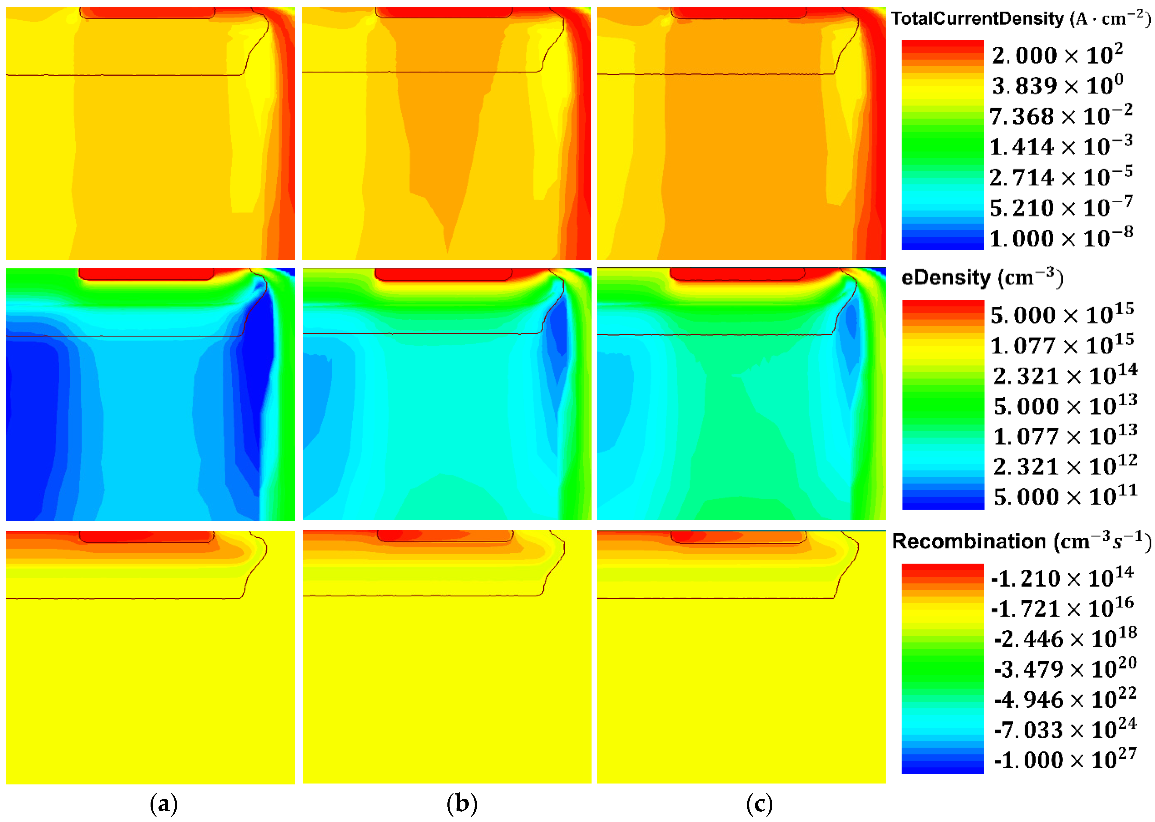
Figure 10a shows the for the various p-base doping concentrations ranging from to . As the increased, the failure of the DUT occurred more rapidly, as shown in Figure 10b. This can explain why the depletion region between the source region and p-base region spread more widely to the p-base region. In addition, the holes in the p-base region diffused to the depletion region. This indicates that the holes in the p-base were not sufficient for a full recombination with the electrons. The parasitic BJT turned on and the current that flowed across the p-base region increased gradually, as shown in Figure 11.
4. Conclusions
The UIS TCAD circuit simulation was performed for various doping concentrations of each region of a SiC MOSFET device. The higher doping concentration of the p-base and source regions, were lower than that of the source region, making the device more stable under the UIS condition. It should be noted that, for the design of the power MOSFET, not only the static characteristics could be considered but also the dynamic characteristics of the device which are used in power applications, such as in a traction inverter. Additionally, the avalanche ruggedness of the device could be expected before the UIS test. Additionally, the circuit design should be investigated by connecting extra free-wheeling diodes to improve the dynamic characterization of SiC power MOSFETs and future device technologies.
Author Contributions
Conceptualization, M.-S.J. and H.-J.L.; methodology, M.-S.J. and H.-J.L.; software, M.-S.J.; validation, H.-J.L.; formal analysis, M.-S.J., J.-H.J. and H.-J.L.; investigation, M.-S.J. and J.-H.J.; data curation, M.-S.J. and J.-H.J.; writing—original draft preparation, M.-S.J.; writing—review and editing, H.-J.L.; project administration, H.-J.L. All authors have read and agreed to the published version of the manuscript.
Funding
This paper was supported by a Korea Institute for Advancement of Technology(KIAT) grant funded by the Korean Government (MOTIE) (P0012451, The Competency Development Program for Industry Specialist). And the EDA tool was supported by the IC Design Education Center (IDEC), Korea.
Institutional Review Board Statement
Not applicable.
Informed Consent Statement
Not applicable.
Data Availability Statement
All the data is presented in this paper.
Conflicts of Interest
The authors declare no conflict of interest.
References
- Baliga, B.J. Fundamentals of Power Semiconductor Devices; Springer: Berlin/Heidelberg, Germany, 2019. [Google Scholar]
- Elasser, A.; Chow, T.P. Silicon carbide benefits and advantages for power electronics circuits and systems. Proc. IEEE 2002, 90, 969–986. [Google Scholar] [CrossRef]
- Kimoto, T.; Cooper, J.A. Fundamentals of Silicon Carbide Technology: Growth, Characterization, Devices and Applications; Wiley: Hoboken, NJ, USA, 2014. [Google Scholar]
- Baliga, B.J. Gallium Nitride and Silicon Carbide Power Devices; World Scientific Publishing: Singapore, 2017; pp. 347–349. [Google Scholar]
- She, X.; Huang, A.Q.; Lucia, O.; Ozpineci, B. Review of silicon carbide power devices and their applications. IEEE Trans. Ind. Electron. 2017, 64, 8193–8205. [Google Scholar] [CrossRef]
- Roccaforte, F.; Fiorenza, P.; Greco, G.; Nigro, R.L.; Giannazzo, F.; Iucolano, F.; Saggio, M. Emerging trends in wide band gap semiconductors (SiC and GaN) technology for power devices. Microelectron. Eng. 2018, 187–188, 66–77. [Google Scholar] [CrossRef]
- Bai, Z.; Tang, X.; Xie, S.; He, Y.; Yuan, H.; Song, Q.; Zhang, Y. Investigation on Single Pulse Avalanche Failure of 1200-V SiC MOSFETs via Optimized Thermoelectric Simulation. IEEE Trans. Electron Devices 2021, 6, 1168–1175. [Google Scholar] [CrossRef]
- Dchar, I.; Zolkos, M. Robustness of SiC MOSFET under Avalanche Conditions. In Proceedings of the Annual IEEE Conference on Applied Power Electronics Conference and Exposition (APEC), Orlando, FL, USA, 19–23 March 2017. [Google Scholar]
- Fischer, K.; Shenai, K. Dynamics of power MOSFET switching under unclamped inductive loading conditions. IEEE Trans. Electron Devices 1996, 43, 1007–1015. [Google Scholar] [CrossRef]
- Fayyaz, A.; Yang, L.; Castellazzi, A. Transient robustness testing of silicon carbide (SiC) power MOSFETs. In Proceedings of the Power Electronics and Applications (EPE), Lille, France, 2–6 September 2013; pp. 1–10. [Google Scholar] [CrossRef]
- Castellazzi, A.; Kartal, V.; Kraus, R.; Seliger, N.; Honsberg-Riedl, M.; Schmitt-Landsiedel, D. Hotspot Meaurements and Analysis of ElectroThermal Effects in Low-Voltage Power-MOSFET’s. Microelectron. Reliab. 2003, 43, 1877–1882. [Google Scholar] [CrossRef]
- Ren, N.; Wang, K.L.; Wu, J.; Xu, H.; Sheng, K. Failure mechanism analysis of SiC MOSFETs in unclamped inductive switching conditions. In Proceedings of the International Symposium on Power Semiconductor Devices and ICs (ISPSD), Shanghai, China, 19–23 May 2019; pp. 183–186. [Google Scholar] [CrossRef]
- Castellazzi, A.; Romano, G.; Urresti, J. UIS failure mechanism of SiC power MOSFETs. In Proceedings of the 4th Workshop on Wide Bandgap Power Devices and Applications (WiPDA), Fayetteville, AR, USA, 7–9 November 2016; IEEE Publications: New York, NY, USA, 2016. [Google Scholar]
- Lien, W.; Damrongplasit, N.; Paredes, J.H.; Senesky, D.G.; Liu, T.K.; Pisano, A.P. 4H-SiC N-Channel JFET for operation in high-temperature environments. IEEE J. Electron Devices Soc. 2014, 2, 164–167. [Google Scholar] [CrossRef]
- Touloukian, Y.S.; Buyco, E.H. Specific heat nonmetallic solids. In Thermophysical Properties Matter; IFI/Plenum: New York, NY, USA, 1970; Volume 5, pp. 448–450. [Google Scholar]
- An, J.; Namai, M.; Okamoto, D.; Yano, H.; Tadano, H.; Iwamuro, N. Investigation of Maximum Junction Temperature for 4H‐SiC MOSFET During Unclamped Inductive Switching Test. Electron. Commun. Jpn. 2018, 101, 24–31. [Google Scholar] [CrossRef]
- Kakarla, B.; Nida, S.; Mueting, J.; Ziemann, T.; Kovacevic-Badstuebner, I.; Grossner, U. Trade-off analysis of the p-base doping on ruggedness of SiC MOSFETs. Microelectron. Reliab. 2017, 76–77, 267–271. [Google Scholar] [CrossRef]
Figure 1.
Unclamped inductive switching (UIS) test circuit.

Figure 2.
(a) Simulated UIS single gate pulse ( waveform; (b) simulated UIS temperature waveform (before failure); (c) simulated UIS and waveforms (before failure); ; .
Figure 2.
(a) Simulated UIS single gate pulse ( waveform; (b) simulated UIS temperature waveform (before failure); (c) simulated UIS and waveforms (before failure); ; .
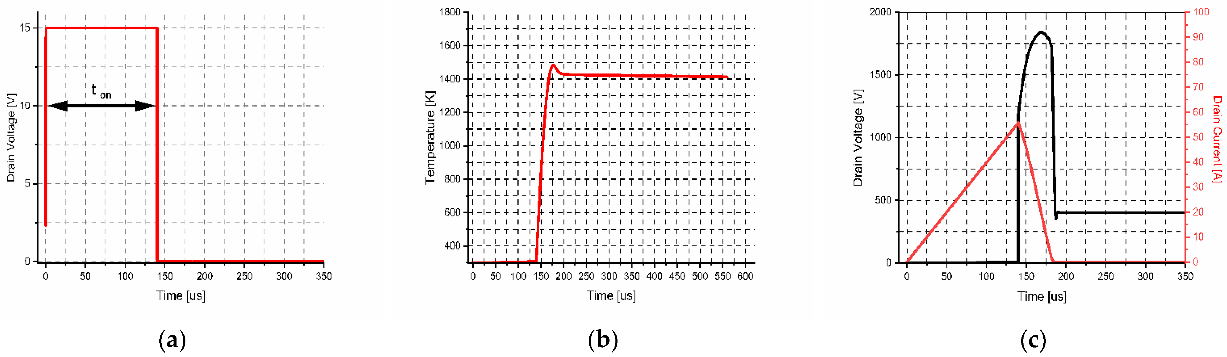
Figure 3.
Power MOSFET structure.

Figure 4.
(a) Simulated UIS and waveforms (at failure); (b) simulated UIS temperature waveform (at failure); ; .
Figure 4.
(a) Simulated UIS and waveforms (at failure); (b) simulated UIS temperature waveform (at failure); ; .

Figure 5.
(a) Simulated UIS for various waveforms; (b) simulated UIS for various waveforms; ; .
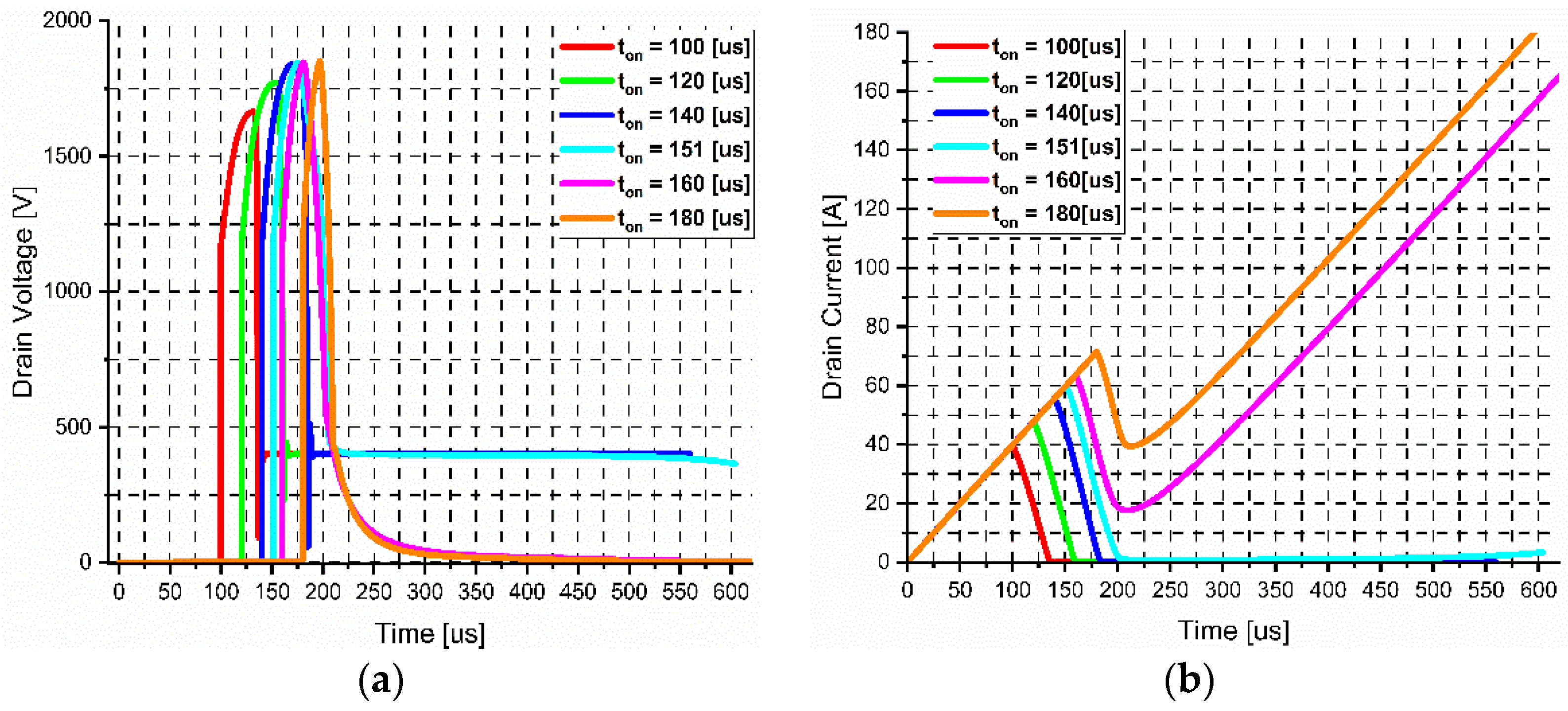
Figure 6.
(a) Simulated UIS for various waveforms; (b) simulated UIS for various waveforms; ; .
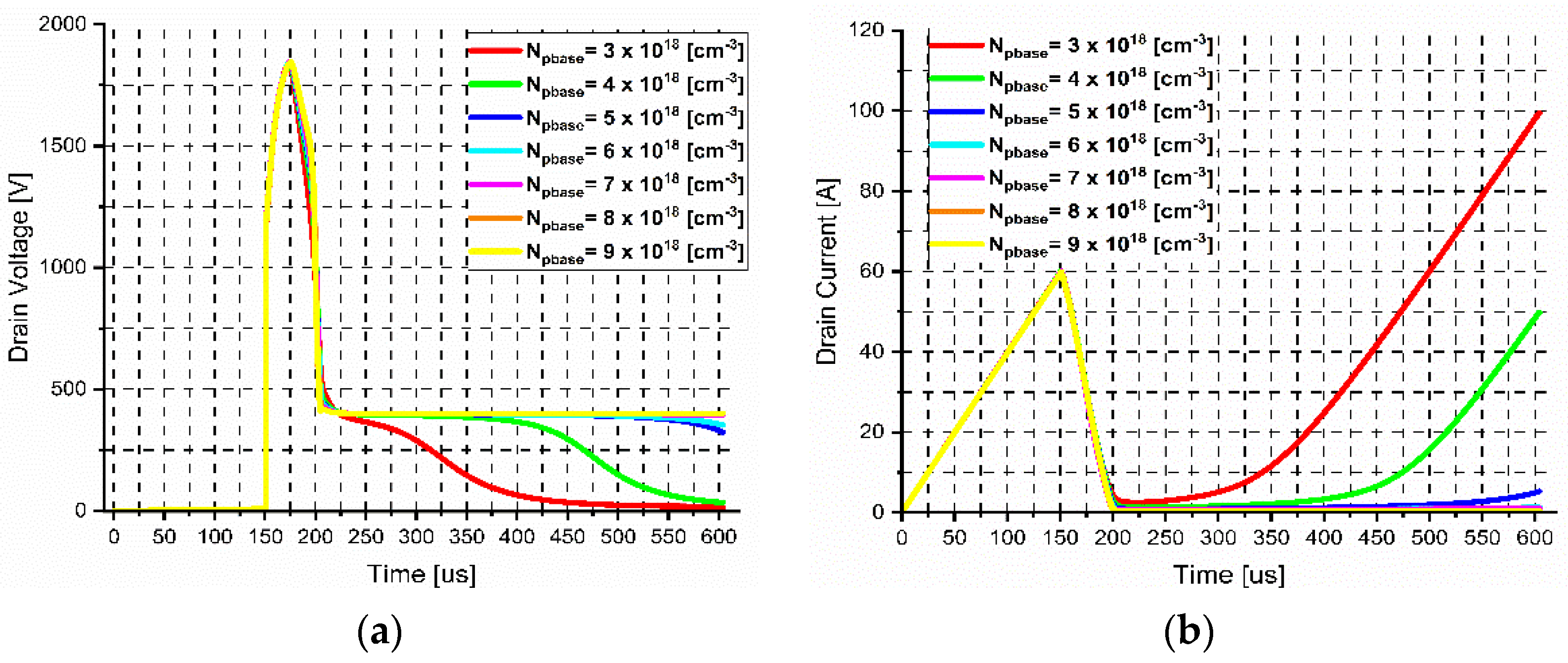
Figure 7.
Total current density, electron density and recombination distribution; (a) , (b) and (c) .
Figure 7.
Total current density, electron density and recombination distribution; (a) , (b) and (c) .
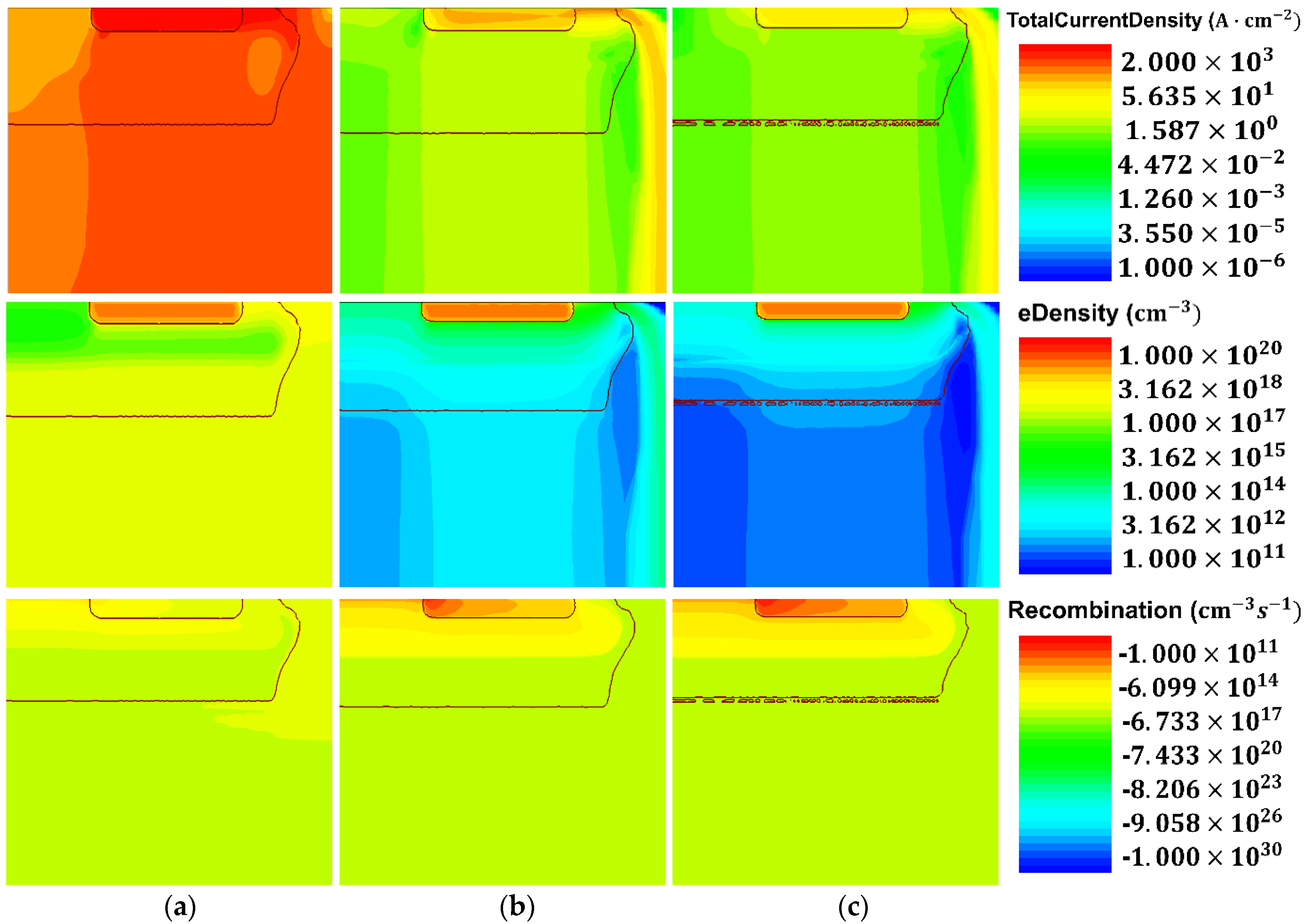
Figure 8.
(a) Simulated UIS for various waveforms; (b) simulated UIS for various waveforms; ; .
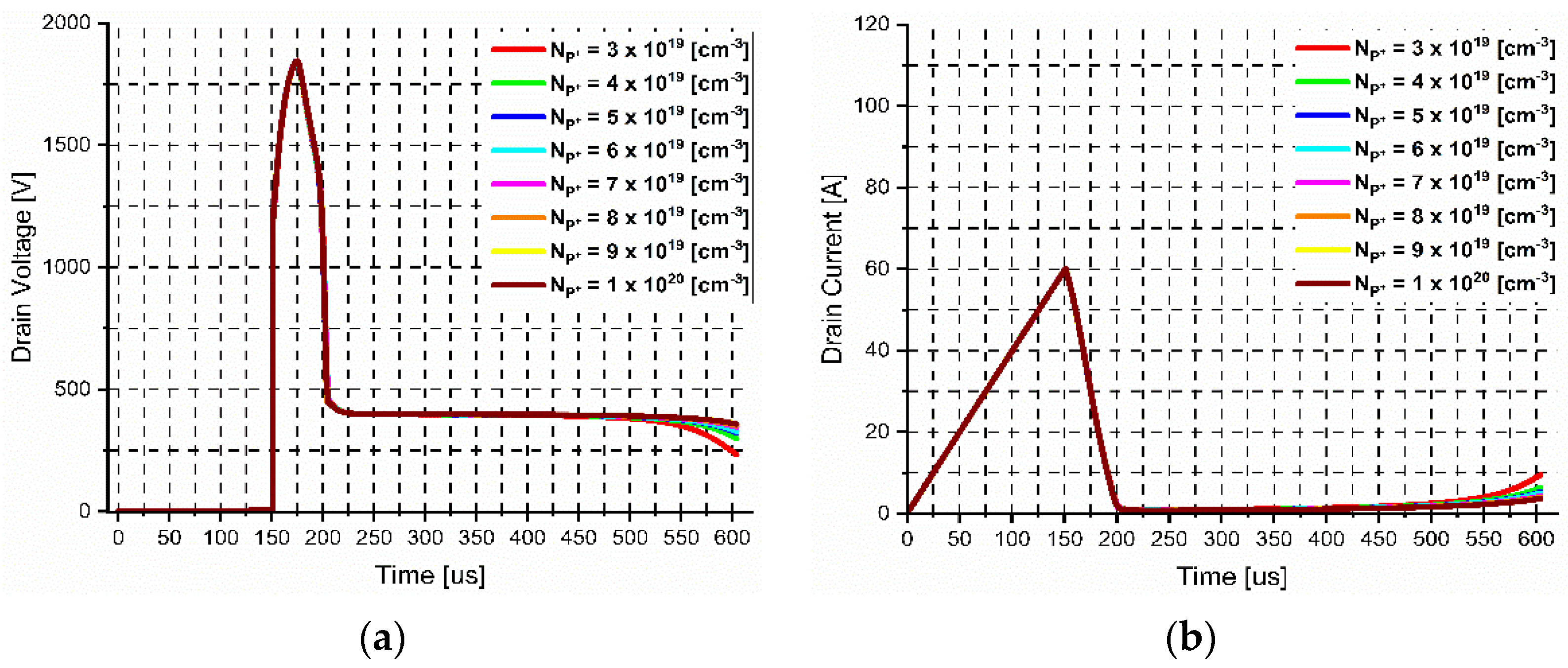
Figure 9.
Total current density, electron density and recombination distribution. (a) , (b) , and (c) .
Figure 9.
Total current density, electron density and recombination distribution. (a) , (b) , and (c) .
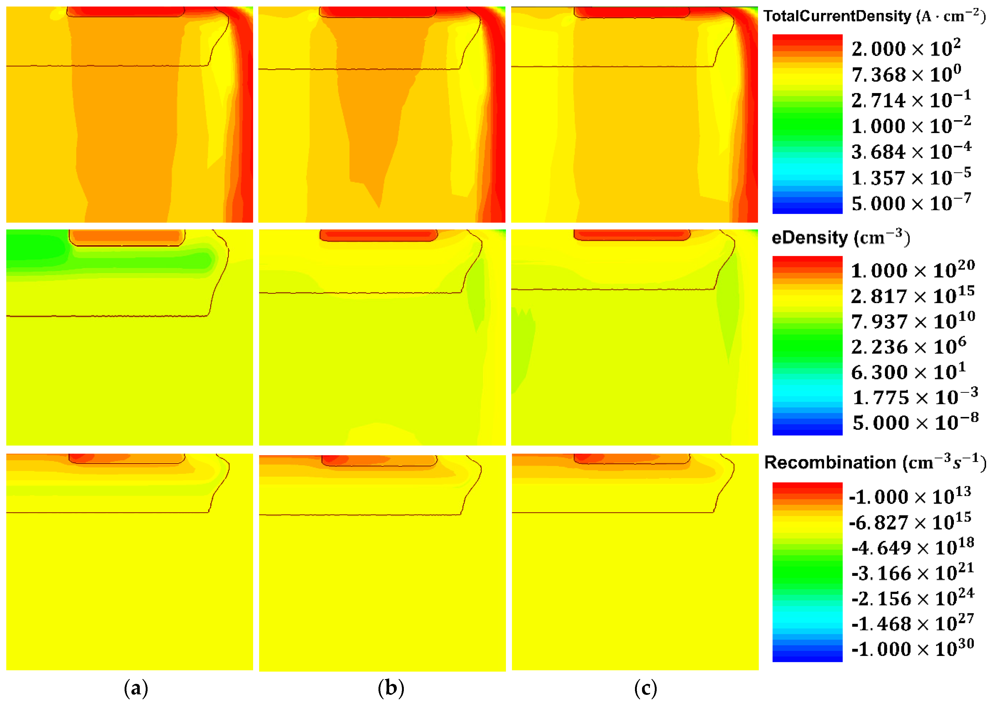
Figure 10.
(a) Simulated UIS for various waveforms; (b) simulated UIS for various waveforms; ; .
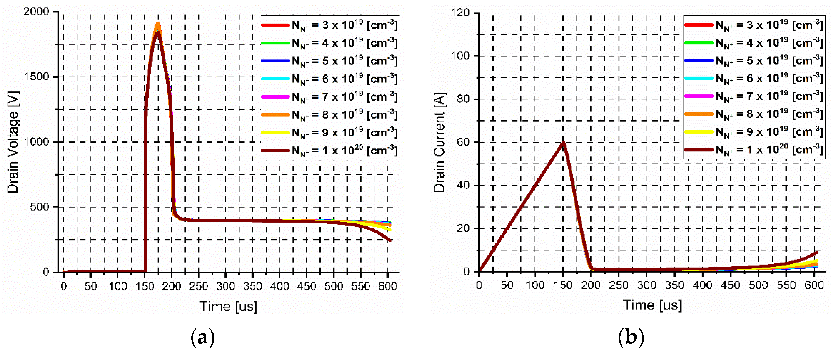
Figure 11.
Total current density, electron density and recombination distribution. (a) , (b) , and (c) .
Figure 11.
Total current density, electron density and recombination distribution. (a) , (b) , and (c) .

Table 1.
Experimental Data of Thermal Dynamic Parameter.
| Heat Capacity | |
|---|---|
| a | |
| b | |
| c | |
| d | |
Disclaimer/Publisher’s Note: The statements, opinions and data contained in all publications are solely those of the individual author(s) and contributor(s) and not of MDPI and/or the editor(s). MDPI and/or the editor(s) disclaim responsibility for any injury to people or property resulting from any ideas, methods, instructions or products referred to in the content. |
© 2022 by the authors. Licensee MDPI, Basel, Switzerland. This article is an open access article distributed under the terms and conditions of the Creative Commons Attribution (CC BY) license (https://creativecommons.org/licenses/by/4.0/).
Share and Cite
MDPI and ACS Style
Jang, M.-S.; Jeong, J.-H.; Lee, H.-J. Analysis of Ruggedness of 4H-SiC Power MOSFETs with Various Doping Parameters. Appl. Sci. 2023, 13, 427. https://doi.org/10.3390/app13010427
AMA Style
Jang M-S, Jeong J-H, Lee H-J. Analysis of Ruggedness of 4H-SiC Power MOSFETs with Various Doping Parameters. Applied Sciences. 2023; 13(1):427. https://doi.org/10.3390/app13010427
Chicago/Turabian StyleJang, Min-Seok, Jee-Hun Jeong, and Ho-Jun Lee. 2023. "Analysis of Ruggedness of 4H-SiC Power MOSFETs with Various Doping Parameters" Applied Sciences 13, no. 1: 427. https://doi.org/10.3390/app13010427
Note that from the first issue of 2016, this journal uses article numbers instead of page numbers. See further details here.