
FPGA Implementation of a Novel Multifunction Modulo (2n ± 1) Multiplier Using Radix-4 Booth Encoding Scheme

Department of Electronic Engineering, National Quemoy University, Kinmen 892, Taiwan
*
Author to whom correspondence should be addressed.
Appl. Sci. 2023, 13(18), 10407; https://doi.org/10.3390/app131810407
Submission received: 10 July 2023
/
Revised: 8 September 2023
/
Accepted: 14 September 2023
/
Published: 18 September 2023
(This article belongs to the Topic Innovation of Applied System)
Abstract
:The residue number system is widely used in applications such as communication systems, cryptography, digital filters, digital signal processors, fault-tolerant detection, and so on. This paper proposes a multifunction modulo (2n ± 1) multiplier based on the radix-4 Booth encoding scheme that can operate both modulo (2n − 1) and modulo (2n + 1) multipliers using the same hardware structure with only one control signal. A novel modulo (2n ± 1) multiplier based on radix-4 Booth encoding is proposed that can achieve superior performance, with low power, fast operation, high area efficiency, and low area-delay product (ADP) and power-delay product (PDP) compared with similar modified Booth-encoding methods. In addition, by integrating the separate modulo functions of the modulo (2n − 1) multiplier and modulo (2n + 1) multiplier into a single multifunction modulo (2n ± 1) multiplier, the proposed method can save up to 52.59% (n = 16) of hardware area, up to 5.45% (n = 32) of delay time, up to 49.05% (n = 16) of dynamic power, up to 50.92% (n = 32) of ADP, and up to 50.02% (n = 32) of PDP compared with the original separate circuits merged together. Furthermore, the operation ranges of the multiplicand and multiplier of the proposed modulo (2n + 1) multiplier and modulo (2n − 1) multiplier are {0, 2n + 1} and {0, 2n}, respectively, which are wider than for other reported hardware structures. The hardware area, power consumption, and delay time are simulated and verified using Verilog HDL and Xilinx FPGA (Field Programmable Gate Array) Vivado tools. The Xilinx Artix-7 XC7A35T-CSG324-1 FPGA chipset is adopted in the proposed work.
1. Introduction
The residue number system (RNS) [1,2,3,4,5,6,7,8,9,10,11] has been widely used in the field of cryptography [10] for purposes such as Fermat number transform [12], elliptic curve ciphers [4,13], Caesar ciphers [4], IDEA (International Data Encryption Algorithm) [13] block ciphers and asymmetric encryption [10] algorithms. The parallel carry-free feature of the RNS will speed up arithmetic operation when the RNS is applied over a binary-based system, thereby greatly reducing the propagation delay and hardware cost of the system. Therefore, the RNS has found wide application in communication systems, digital signal processors [6], digital filters [3], finite-impulse response (FIR) filters [3,7], fast Fourier transform (FFT) [7], fault-tolerant detection [11], error correction coding [11,14] and other fields [12]. Parallel-prefix adders [15] can provide a very efficient modulo arithmetic operation in RNS mathematical computation. Parallel-prefix adders [15] such as Kogge Stone adder, Sklansky adder, Ladner Fischer adder and Ling’s adder are some of the most commonly used circuit architectures in modular operation.
Modulo (2n + 1) multipliers [2,13,16,17,18,19,20,21], modulo (2n − 1) multipliers [1,8,21,22,23,24], modulo (2n + 1) adders [15,25,26] and modulo (2n − 1) subtractors [26], which are ROM (Read Only Memory)-less modular arithmetic operations, are most commonly used. Many modular multiplication methods have been reported, such as diminished-1modulo multiplication [12,15,16,27,28], weighted modulo multiplication [2,19,26,29], and Booth-encoder multiplication [8,30]. Diminished-1 and weighted representations are commonly used in modulo (2n − 1) and modulo (2n + 1) multipliers. For the diminish-1 and weighted representation, n bits are required for the numbers [0, 2n − 1] and n + 1 bits are needed for the numbers [0, 2n], respectively. For diminished-1 modular multiplication [12,15,16,27,28], 1 needs to be subtracted from both the multiplicand and multiplier during operation; therefore, the multiplicand and multiplier cannot be 0 and their operation range is only [1, 2n − 1]. Thus, it is important to use an additional conversion circuit and a zero detection circuit, as well as to add back one adder after processing the sum of all the partial products. However, this will increase the hardware area, power consumption, and delay time in the design of diminished-1 modulo multiplication. To address these shortcomings, the weighted modular multiplication architecture was proposed [2,19,26,29], which has an improved operation range of [0, 2n] and greatly reduces the delay time and circuit area. It is worth noting that the zero-detection circuit is not required for weighted modular multiplication. Booth-encoder modular multiplication, which uses two bits as the multiplier in operation, can further reduce the area and delay compared to weighted modular multiplication. The partial product of radix-4 Booth-encoder modular multiplication [8,30], which uses three bits as the multiplier, is reduced by nearly half compared to that of conventional Booth-encoder modular multiplication. This will considerably reduce the use of the full adder, thereby minimizing the circuit area and delay time.
This study proposes an FPGA implementation of multifunction modulo (2n ± 1) multiplier based on radix-4 Booth encoding that can operate both the modulo (2n + 1) multiplier and modulo (2n − 1) multiplier in the same hardware. Juang and Huang [8] presented a modified Booth-encoder-based multifunction modulo (2n ± 1) multiplier using the structure of a modified Booth-coded 1′s complement modulo (2n − 1) multiplier [1] and a modified Booth-based modulo (2n + 1) multiplier [18] and combined them into a multifunction modulo (2n ± 1) multiplier. However, their hardware structure still has room for improvement in terms of the power consumption, delay time, hardware area, and operation range. The architecture of the radix-4 Booth-encoding-based multifunction modulo (2n ± 1) multiplier proposed in this paper can achieve significant improvements in power consumption, latency, hardware area, and operation range. The proposed modular multiplication can greatly reduce the hardware cost, delay time, and power consumption, while having wider operation ranges compared to that of Juang and Huang’s method [8]. In this article, the circuit design and implementation are carried out using an FPGA (Field Programmable Gate Array) [3]. FPGA is a popular and important electronic device that can be easily corrected, reusable and reprogrammable by a designer. The advantages of FPGA are that it is easier to be implemented and configured by logic circuit, has a shorter time to develop a prototype circuit and has a lower price than conventional ASICs (Application Specific Integrated circuits). Based on these advantages, FPGA is widely used for circuit prototyping and product development. In the proposed FPGA-based multifunction modulo (2n ± 1) multiplier using the radix-4 Booth scheme, the abovementioned delay time, hardware area and power are simulated and verified using Xilinx FPGA (Field Programmable Gate Array) Vivado tools. The target chip is implemented using a Xilinx Artix-7 XC7A35T-CSG324-1 FPGA in the proposed work.
The rest of this paper is structured as follows. Section 2 describes the methods reported in the literature. Section 3 presents the proposed radix-4 Booth-encoding-based multifunction modulo (2n ± 1) multiplier design, which is the area-delay-power efficient. Section 4 presents the results of the proposed method in comparison with those of various other methods. Finally, Section 5 summarizes the study.
2. Related Work
This section reviews radix-4 Booth-encoding-based modulo (2n + 1) and modified Booth-encoding-based modulo (2n − 1) multipliers, as well as multifunction modulo (2n ± 1) multipliers based on the modified Booth encoding scheme [8]. Unlike the traditional Booth encoder, which uses double-code interpretation, the modified Booth encoder, also called radix-4 Booth encoding, adopts a three-code interpretation. First, 0 is added after the least significant bit of the multiplier and 0 is also added in front of the most significant bit of the multiplier. This three-code interpretation method substantially reduces the partial product, which almost halves the hardware area. As a result, the significant reduction in the use of the full adder facilitates faster calculations. The modulo (2n + 1) multipliers and modulo (2n − 1) multipliers are the two most commonly used in the RNS, and these will be reviewed in the following paragraphs.
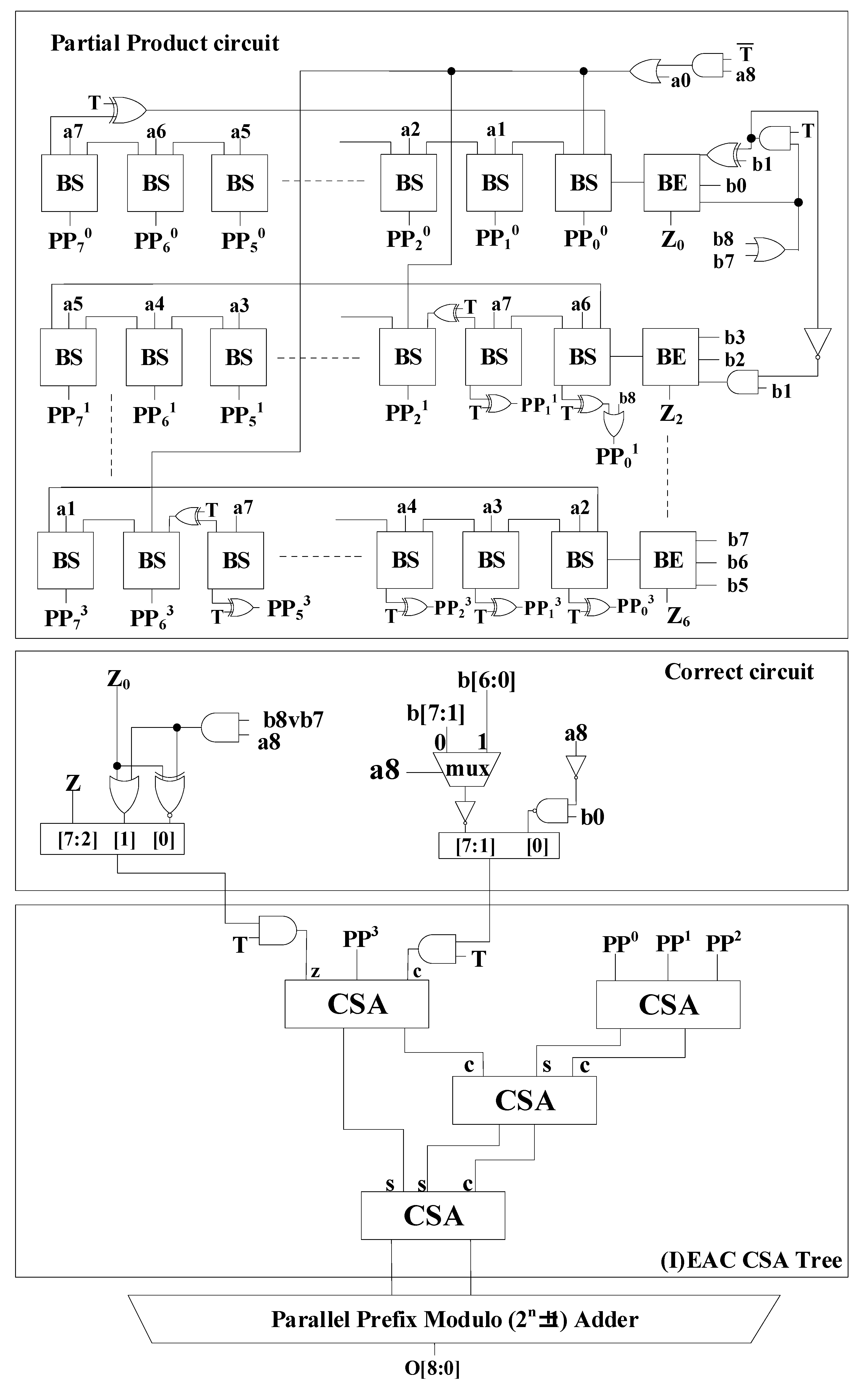
The operating range of the modified Booth-coded 1′s complement modulo (2n − 1) multiplier [1] is [0, 2n − 1]. The block diagram of modulo multiplication using modified Booth encoding is shown in Figure 1. Multiplier B first performs improved Booth encoding (BE) and multiplicand A operates a Booth selector (BS) according to the encoded value. Subsequently, the addition array of partial products is generated and these partial products are summed by the full and half adders. Finally, the result is obtained by performing end-around-carry. The relative formula found using the modified Booth-encoder-based 1’s complement modulo (2n − 1) multiplier is given by
The system block of modified Booth-coded 1′s complement modulo (2n − 1) multipliers is shown in Figure 2, where n is set to 8; therefore, it is the block diagram of the modified Booth-encoding-based modulo 63 multiplier [1]. In Figure 2b,c, the ×1 and ×2 of the Booth encoder and Booth selector are used to multiply by 1 and 2, respectively. The sign signal is used to determine positive or negative based on the modified Booth encoding regulation. Multiplier B adopts a three-code interpretation in operation, so the logic circuit diagram of BE in Figure 2b can be deduced from the operation in Equation (1). When three numbers, b2i−1, b2i, and b2i+1, are inputted, the output can be obtained from the signals multiplied by 1 (×1), multiplied by 2 (×2), and the sign signal. The sign signal is used to determine whether the multiplication output of multiplicand will be positive or negative. When the value of sign is 0, the output of the multiplicand is a positive value; when it is 1, the output of the multiplicand is a negative value. According to Equation (1), multiplier B multiplied by multiplicand A will provide Equation (2), where PPi is its partial product and PPi = A × 22i(b2i−1 + b2i − 2b2i+1).
For modulo (2n + 1) multiplication using modified Booth encoding, a modified Booth-encoding-based modulo (2n + 1) multiplier was proposed [2]. This work adopted weighted architecture and did not require additional subtraction and addition operations, such as the diminished-1 architecture as well as additional conversion circuits and a zero detection circuit. However, an additional weighting circuit is required to obtain the final result. Even so, the performance of this method is still better than that of modified Booth-encoding-based modulo multiplication using the diminished-1 architecture. The block diagram of the modified Booth-based modulo 65 (2n + 1) multiplier [2], with n set to 8 is shown in Figure 3. Here, the Booth encoder, Booth selector, half adder, and full adder in the hardware structure are abbreviated as BE, BS, HA, and FA, respectively. In this work [2], the multiplicand A and multiplier B are expressed in binary as A = an an−1 an−2… a0 and B = bn bn−1 bn−2… b0. The final result Q [2] can be expressed as Equation (3):
where .
According to Equation (3), the BE and BS are shown in Figure 4a,b. Equation (3) can be deduced and calculated according to [2] and, finally, Equations (4) and (5) can be obtained:
In these equations, C is carry, S is sum, Zn* and are the compensation values of the weighting circuit used to obtain accurate output values, and pp1* is taken by the inverter of ppi,0−2i−1 (for i > 0). Finally, Equations (4) and (5) are summed using the inverted end-around-carry (IEAC) carry-save adder (CSA) tree to obtain the final output value Q.
From the above descriptions of the modified Booth-encoding modulo (2n − 1) multiplier and modulo (2n + 1) multiplexer, it is clear that the two architectures have many similar circuits. The similar parts of the two architectures can be leveraged as a basis for common use. A certain method can be used to distinguish the different operations so that a circuit with a slightly larger hardware can be used to complete the two kinds of modulus operations. Juang and Huang [8] also adopted the modified Booth-coded 1 complement modulo (2n − 1) multiplier [1] and modified Booth-encoding-based modulo (2n + 1) multiplier [18] and combined them into the multifunction modulo (2n ± 1) multiplier using the same hardware. However, their hardware structure still has room for improvement in terms of power consumption, delay time, hardware area, and operation range. The architecture of the radix-4 Booth-encoding-based multifunction modulo (2n ± 1) multiplier proposed in this paper can achieve significant improvements in power consumption, latency, and hardware area. Moreover, the structure of the proposed low-power, area-saving, and fast modulo (2n ± 1) multiplier can operate the modulo (2n + 1) and modulo (2n − 1) multipliers with only one control signal sharing the same hardware structure. Meanwhile, the operation ranges of the multiplicand and multiplier of the proposed modulo (2n + 1) and modulo (2n − 1) multipliers are {0, 2n + 1} and {0, 2n}, respectively. These ranges are wider than those of the hardware structure reported by Juang and Huang [8]. The system architecture of the proposed FPGA implementation of multifunction modulo (2n ± 1) multiplier based on radix-4 Booth encoding will be presented in the following section.
3. Proposed Modulo (2n ± 1) Multiplier Based on Radix-4 Booth Encoding
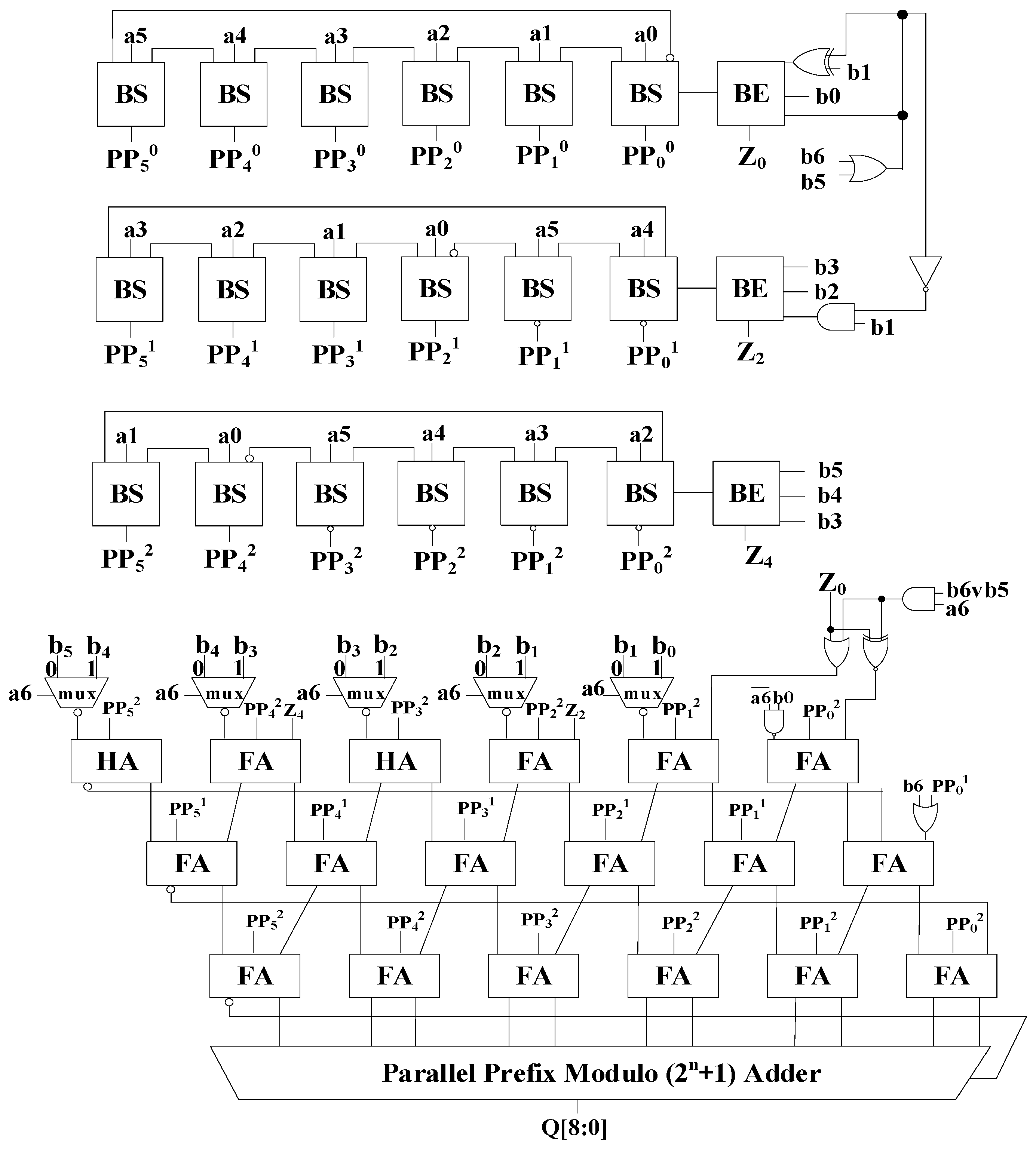
The system architecture of the proposed modulo (2n ± 1) multiplier based on radix-4 Booth-encoding is shown in Figure 5. The proposed modulo (2n ± 1) multipliers can support modulo (2n + 1) and modulo (2n − 1) multiplication functions in the same circuit hardware. Compared with the traditional modulo (2n + 1) or modulo (2n − 1) multipliers, the proposed multipliers can use the same architecture to distinguish between two different operations by selecting signal T. When T = 1, the modulo (2n + 1) multiplier is selected and, when T = 0, the modulo (2n − 1) multiplier is selected. The operation ranges of the multiplicand and multiplier are {0, 2n + 1} and {0, 2n} for the modulo (2n + 1) multiplier and modulo (2n − 1) multipliers, respectively. The proposed modulo (2n ± 1) multiplier system architecture, shown in Figure 5, includes a partial product circuit unit, a correct circuit unit, an IEAC CSA tree, and a parallel prefix modulo (2n ± 1) adder. For the partial product circuit unit, the circuit architectures of BE and BS use the same circuit reported in [2], as shown in Figure 4. For each BS row array in the partial product, in the specific BS block with a7 input, the output signal is XOR with selection signal T, and the output of the XOR gate will feed into the next BS block stage. To increase the operating range of the modulo (28 + 1) and modulo (28 − 1) multipliers (for modulo (2n + 1) and modulo (2n − 1) multipliers, n is set to 8), as shown in Figure 5, the OR gate is used to connect b8 and b7 and the output of this OR gate will be subjected to an AND gate with selection signal T for the BE input of the first row and second row in the partial product block. An appropriate circuit unit is used to produce the compensation values for obtaining accurate output values for modular multiplication operations using modified Booth-encoding schemes. In the IEAC part, for the structure of the modulo (2n − 1) multiplexer, the original value of end-around-carry is retained. For the structure of the modulo (2n + 1) multiplexer, the original value of end-around-carry will be reversed. The proposed improved parallel prefix adder of modulo (2n ± 1) multipliers based on radix-4 Booth encoding (n = 8) is shown in Figure 6. Assuming that the T signal passes through the XOR gate, when the signal is 0, the modulo (2n − 1) adder is calculated, and when the signal is 1, the modulo (2n + 1) adder is calculated.
As an example of the proposed multifunction modulo (2n ± 1) multiplier based on radix-4 Booth encoding, n = 8 is chosen. Figure 7a,b show the operation process of the proposed modulo (2n ± 1) multiplier. For the modulo (2n − 1) multiplication operation with T = 0, A = 256, and B = 256, the final result is 1 (Figure 7a) and, for the modulo (2n + 1) multiplication operation with T = 1, A = 256, and B = 256, the final result will be 1 (Figure 7b).
In the next section, the proposed FPGA implementation of radix-4 Booth-encoding-based multifunction modulo (2n ± 1) multipliers are experimentally analyzed, and the results are compared with those of other methods in terms of the operation range, area, delay time, dynamic power, area-delay product (ADP), and power-delay product (PDP).
4. Experimental Results and Comparison
The experimental results obtained using the proposed structure of multifunction modulo (2n ± 1) multipliers based on radix-4 Booth encoding, as explained in Section 3, are discussed in this section. The term ‘merge circuits’ is used to represent the incorporated circuits that can support two different types of modular multiplication functions adopted by the modulo (2n − 1) [1] and modulo (2n + 1) [2] multipliers. The proposed multifunction modulo (2n ± 1) multipliers can support the aforementioned modular multiplication functions in the same circuit hardware. Table 1 compares the operation ranges of the proposed method and other reported methods. The operation ranges of the multiplicand and multiplier of the proposed modulo (2n + 1) and modulo (2n − 1) multipliers are {0, 2n + 1} and {0, 2n}, respectively; these ranges are wider than those of Juang and Huang’s [8] reported hardware structure. The integration of the single modulo functions of the modulo (2n + 1) multipliers and modulo (2n − 1) multipliers into a multifunction modulo (2n ± 1) multiplier can save up to 52.59% (n = 16) of the hardware area, as shown in Table 2. As shown in Table 3, compared with that of the original single circuit performing the function of the modulo (2n − 1) multiplier [1] or modulo (2n + 1) multiplier [2] exclusively, the delay time of the proposed method slightly increased for n = 8 and 16 but slightly decreased for n = 32. The delay time of the proposed method is considerably lower than that of Juang and Huang’s [8] method. For the merged circuits, as shown in Table 3, it should be noted that the merged delay time of the modulo (2n − 1) [1] and modulo (2n + 1) [2] multipliers would be selected to be the worst case for the two of them. As Table 4 shows, the dynamic power consumption of the proposed study can be reduced by 44.19% (n = 8) to 49.05% (n = 16). As Table 5 shows, the ADP can be reduced by 38.90% (n = 8) to 50.92% (n = 32). As Table 6 shows, the PDP can be reduced by up to 50.02% (n = 32). It should be noted that the aforementioned ADP and PDP of the merged circuits are defined as the sums of the individual ADPs and PDPs, respectively, of the modulo (2n − 1) [1] multipliers and modulo (2n + 1) [2] multipliers. In Table 1, Table 2, Table 3, Table 4, Table 5 and Table 6, it is clear that the proposed modulo (2n ± 1) multiplier based on radix-4 Booth encoding outperforms other modified Booth methods by exhibiting a wider operation range, lower power consumption, faster operation, better area efficiency, and lower ADP and PDP. The hardware area, power consumption, and delay time are simulated, synthesized, and verified using Verilog HDL and Xilinx FPGA Vivado tools. The Xilinx Artix-7 XC7A35T-CSG324-1 FPGA chipset is adopted. The operating clock frequency, voltage and junction temperature in the simulation are 100 MHz, 3.3 V and 25.4 °C, respectively.
5. Conclusions
This study improved the performance of Juang and Huang’s modified Booth-encoder-based multifunction modulo (2n ± 1) multiplier [8] by basing it on a radix-4 Booth encoding scheme to have a wider operation range, lower power consumption, faster operation, better area efficiency, and lower area-delay product (ADP) and power-delay product (PDP). It can support the multiplication functions of both modulo (2n + 1) and modulo (2n − 1) multiplexers in the same circuit hardware. By integrating their single modulo functions into a multifunction modulo (2n ± 1) multiplier, it can save up to 50.92% (n = 32) of ADP and 50.02% (n = 32) of PDP compared with merged separate circuits. This multifunction modulo multiplier can be applied to communication systems, cryptography, digital filters, and digital signal processors.
Author Contributions
Conceptualization, C.-T.K. and Y.-C.W.; Methodology, C.-T.K. and Y.-C.W.; Software, Y.-C.W.; Validation, C.-T.K. and Y.-C.W.; Formal analysis, C.-T.K.; Investigation, C.-T.K. and Y.-C.W.; Writing—original draft, C.-T.K.; Writing—review & editing, C.-T.K. All authors have read and agreed to the published version of the manuscript.
Funding
This research received no external funding.
Institutional Review Board Statement
“Not applicable” for studies not involving humans or animals.
Informed Consent Statement
Not applicable.
Data Availability Statement
Not applicable.
Conflicts of Interest
The authors declare no conflict of interest.
References
- Vergos, H.T.; Efstathiou, C. Modified Booth 1’s Complement and Modulo 2n − 1 Multipliers. In Proceedings of the 7th IEEE International Conference on Electronics, Circuits and Systems (ICECS), Jounieh, Lebanon, 17–20 December 2000; pp. 637–640. [Google Scholar]
- Efstathou, C.; Moshopoulos, N.; Axelos, N.; Pekmestzi, K. Efficient modulo 2n + 1 multiply and multiply-add units based on modified Booth encoding. Integration 2014, 47, 140–147. [Google Scholar] [CrossRef]
- Kaluri, K.; Leong, W.F.; Tan, K.H.; Johnson, L.; Soderstrand, M. FPGA hardware implementation of an RNS FIR digital filter. In Proceedings of the Conference Record of Thirty-Fifth Asilomar Conference on Signals, Systems and Computers (Cat.No.01CH37256), Pacific Grove, CA, USA, 4–7 November 2001; pp. 1340–1344. [Google Scholar]
- Schinianakis, D.M.; Fournaris, A.P.; Michail, H.E.; Kakarountas, A.P.; Stouraitis, T. An RNS implementation of an Fp elliptic curve point multiplier. IEEE Trans. Circuits Syst. I Regul. Pap. 2009, 56, 1202–1213. [Google Scholar] [CrossRef]
- Ma, S.; Hu, S.; Yang, Z.; Wang, X.; Liu, M.; Hu, J. High Precision Multiplier for RNS {2n − 1, 2n, 2n + 1}. Electronics 2021, 10, 1113. [Google Scholar] [CrossRef]
- Ramirez, J.; Garcia, A.; Lopez-Buedo, S.; Lloris, A. RNS-enabled Digital Signal Processor Design. Electron. Lett. 2002, 38, 266–268. [Google Scholar] [CrossRef]
- Nannarelli, A.; Re, M.; Cardarilli, G.C. Tradeoffs between residue number system and traditional FIR filter. In Proceedings of the IEEE International Symposium on Circuits and Systems (ISCAS), Sydney, NSW, Australia, 6–9 May 2001; pp. 305–308. [Google Scholar]
- Juang, T.B.; Huang, J.H. Multifunction RNS modulo (2n ± 1) Multipliers Based on Modified Booth Encoding. In Proceedings of the 2012 IEEE Asia Pacific Conference on Circuits and Systems, Kaohsiung, Taiwan, 2–5 December 2012; pp. 515–518. [Google Scholar]
- Prediger, V.; Bairros, F.; Seman, L.O.; Bezerra, E.A.; Pettenghi, H. RNS processor using moduli sets of the form 2n ± 1. Int. J. Circuit Theory Appl. 2023, 51, 3432–3442. [Google Scholar] [CrossRef]
- Schoinianakis, D. Residue arithmetic systems in cryptography: A survey on modern security applications. J. Cryptogr. Eng. 2020, 10, 249–267. [Google Scholar] [CrossRef]
- Babenko, M.; Nazarov, A.; Deryabin, M.; Kucherov, N.; Tchernykh, A.; Hung, N.V.; Avetisyan, A.; Toporkov, V. Multiple Error Correction in Redundant Residue Number Systems: A Modified Modular Projection Method with Maximum Likelihood Decoding. Appl. Sci. 2022, 12, 463. [Google Scholar] [CrossRef]
- Sunder, S.; El-Guibaly, F.; Antoniou, A. Area-Efficient diminished-1 multiplier for fermat number-theoretic transform. IEE Proc. G 1993, 140, 211–215. [Google Scholar] [CrossRef]
- Palutla, K.; Gundabathina, P. Implementation of High Speed Modulo (2n + 1) Multiplier for IDEA Cipher. Procedia Comput. Sci. 2020, 171, 2016–2022. [Google Scholar] [CrossRef]
- Kalmykov, I.A.; Pashintsev, V.P.; Tyncherov, K.T.; Olenev, A.A.; Chistousov, N.K. Error-Correction Coding Using Polynomial Residue Number System. Appl. Sci. 2022, 12, 3365. [Google Scholar] [CrossRef]
- Singhal, S.K.; Mohanty, B.K.; Patel, S.K.; Saxena, G. Efficient Diminished-1 Modulo (2n + 1) Adder Using Parallel Prefix Adder. J. Circuits Syst. Comput. 2020, 29, 2050186. [Google Scholar] [CrossRef]
- Vergos, H.T.; Nikolos, D. Efficient Diminished-1 Modulo 2n + 1 Multipliers. IEEE Trans. Comput. 2005, 51, 491–496. [Google Scholar]
- Vergos, H.T.; Efstathiou, C. Design of efficient modulo 2n + 1 multipliers. IET Comput. Digit. Tech. 2007, 1, 49–57. [Google Scholar] [CrossRef]
- Chen, J.W.; Yao, R.H.; Wu, W.J. Efficient modulo 2n + 1 multipliers. IEEE Trans. VLSI Syst. 2011, 19, 2149–2157. [Google Scholar] [CrossRef]
- Juang, T.B.; Wu, G.L.; Chiu, C.C. Design of an area-efficient weighted modulo 2n + 1 multipliers. In Application and Innovation of Prototypes and Circuits; Ching Yun University: Taoyuan City, Taiwan, 2009; pp. 376–381. [Google Scholar]
- Sousa, L.; Chaves, R. A universal architecture for designing efficient modulo 2n + 1 multipliers. IEEE Trans. Circuits Syst. I 2005, 52, 1166–1178. [Google Scholar] [CrossRef]
- Juang, T.B.; Kuo, C.T.; Wu, G.L.; Huang, J.H. Multifuction RNS Modulo 2n ± 1 Multipliers. J. Circuits Syst. Comput. 2012, 21, 1250027. [Google Scholar] [CrossRef]
- Muralidharan, R.; Chang, C.H. Area-Power Efficient Modulo 2n − 1 and Modulo 2n + 1Multipliers for {2n − 1, 2n, 2n + 1} Based RNS. IEEE Trans. Circuits Syst. I Regul. Pap. 2012, 59, 2263–2274. [Google Scholar] [CrossRef]
- Kumar, R.; Jaiswal, R.K.; Mishra, R.A. Perspective and Opportunities of Modulo 2n − 1 Multipliers in Residue Number System: A Review. J. Circuits Syst. Comput. 2020, 29, 2030008. [Google Scholar] [CrossRef]
- Timarchi, S.; Akbarzadeh, N. Area-Time-Power Efficient Maximally Redundant Signed-Digit Modulo 2n − 1 Adder and Multiplier. Circ. Syst. Signal Pract. 2019, 38, 2138–2164. [Google Scholar] [CrossRef]
- Patel, B.K.; Kanungo, J. Efficient Tree Multiplexer Design by using Modulo 2n + 1 adder. In Proceedings of the 2021 Emerging Trends in Industry 4.0 (ETI 4.0), Raigarh, India, 19–21 May 2021. [Google Scholar] [CrossRef]
- Efstathiou, C.; Kouretas, I.; Kitsos, P. On the modulo 2n + 1 addition and subtraction for weighted operands. Microprocess Microsy 2023, 11, 2138–2164. [Google Scholar]
- Patel, B.K.; Kanungo, J. Diminished-1 multiplier using modulo 2n + 1 adder. Int. J. Eng. Technol. 2018, 7, 31–35. [Google Scholar] [CrossRef]
- Lin, S.H.; Sheu, M.H. VLSI design of diminished-one modulo 2n + 1 adder using circular carry selection. IEEE Trans. Circuits Sys. II Express Briefs 2008, 55, 897–901. [Google Scholar]
- Juang, T.B.; Chiu, C.C.; Tsai, M.Y. Improved area-efficient weighted modulo 2n + 1 adders design with simple correction schemes. IEEE Trans. Circuits Sys. II Express Briefs 2010, 57, 198–202. [Google Scholar]
- Muralidharan, R.; Chang, C.H. Radix-4 and Radix-8 Booth Encoded Multi-Modulus Multipliers. IEEE Trans. Circuits Syst. I Regul. Pap. 2013, 60, 2940–2952. [Google Scholar] [CrossRef]
Figure 1.
Block diagram of modulo multiplication using modified Booth encoding [1].
Figure 1.
Block diagram of modulo multiplication using modified Booth encoding [1].

Figure 2.
(a) Hardware structure of the modulo (28 − 1) (63, n = 8) multiplier [1]. (b) Circuit of the Booth encoder [1] and (c) Circuit of the Booth selector [1].

Figure 3.
Hardware structure of the modulo (28 + 1) (65, n = 8) multiplier [2].
Figure 3.
Hardware structure of the modulo (28 + 1) (65, n = 8) multiplier [2].


Figure 5.
Proposed architecture of modulo (2n ± 1) multipliers based on radix-4 Booth encoding (n = 8).
Figure 5.
Proposed architecture of modulo (2n ± 1) multipliers based on radix-4 Booth encoding (n = 8).

Figure 6.
Proposed improved parallel prefix adder of modulo (2n ± 1) multipliers based on radix-4 Booth encoding (n = 8).
Figure 6.
Proposed improved parallel prefix adder of modulo (2n ± 1) multipliers based on radix-4 Booth encoding (n = 8).

Figure 7.
Example of the proposed modulo (2n ± 1) multiplication operation (n = 8). (a) T = 0; (b) T = 1.
Figure 7.
Example of the proposed modulo (2n ± 1) multiplication operation (n = 8). (a) T = 0; (b) T = 1.


Table 1.
Comparison of operation ranges of the proposed method and other methods.
| Item | Merged Circuits [1,2] | Modulo (2n ± 1) [8] | Proposed Work | ||||
|---|---|---|---|---|---|---|---|
| Modulo (2n − 1) [1] | Modulo (2n + 1) [2] | Modulo (2n − 1) | Modulo (2n + 1) | Modulo (2n − 1) | Modulo (2n + 1) | ||
| Operation Range | Multiplicand | {0, 2n − 1} | {0, 2n + 1} | {0, 2n} | {1, 2n + 1} | {0, 2n} | {0, 2n + 1} |
| Multiplier | {0, 2n − 1} | {0, 2n + 1} | {0, 2n} | {0, 2n} | {0, 2n} | {0, 2n + 1} | |
Table 2.
Comparison of the hardware areas of the proposed method and other methods.
| Item | Modulo (2n − 1) [1] | Modulo (2n + 1) [2] | Merged Circuits [1,2] | Modulo (2n ± 1) [8] | Proposed Work | |||
|---|---|---|---|---|---|---|---|---|
| n | Area (LUT) | Area (LUT) | Area (LUT) | Area Saving | Area (LUT) | Area Saving | Area (LUT) | Area Saving |
| 8 | 84 | 103 | 187 | 0 | 113 | +39.57% | 107 | +42.78% |
| 16 | 355 | 358 | 713 | 0 | 382 | +46.42% | 338 | +52.59% |
| 32 | 1406 | 1281 | 2687 | 0 | 1498 | +44.25% | 1284 | +52.21% |
Table 3.
Comparison of the delay times of the proposed method and other methods.
| Item | Modulo (2n − 1) [1] | Modulo (2n + 1) [2] | Merged Circuits [1,2] | Modulo (2n ± 1) [8] | Proposed Work | |||
|---|---|---|---|---|---|---|---|---|
| n | Delay (ns) | Delay (ns) | Delay (ns) | Delay Saving | Delay (ns) | Delay Saving | Delay (ns) | Delay Saving |
| 8 | 13.203 | 15.332 | 15.332 * | 0 | 15.954 | +4.06% | 15.351 | −0.12% |
| 16 | 19.346 | 19.457 | 19.457 * | 0 | 21.219 | +9.06% | 20.729 | −6.54% |
| 32 | 30.532 | 28.565 | 30.532 * | 0 | 33.376 | +9.31% | 28.868 | +5.45% |
Table 4.
Comparison of the dynamic powers of the proposed method and other methods.
| Item | Modulo (2n − 1) [1] | Modulo (2n + 1) [2] | Merged Circuits [1,2] | Modulo (2n ± 1) [8] | Proposed Work | |||
|---|---|---|---|---|---|---|---|---|
| n | Power (W) | Power (W) | Power (W) | Power Saving | Power (W) | Power Saving | Power (W) | Power Saving |
| 8 | 0.042 | 0.044 | 0.086 | 0 | 0.048 | +44.19% | 0.048 | +44.19% |
| 16 | 0.105 | 0.105 | 0.21 | 0 | 0.114 | +45.71% | 0.107 | +49.05% |
| 32 | 0.282 | 0.283 | 0.565 | 0 | 0.309 | +45.31% | 0.289 | +48.85% |
Disclaimer/Publisher’s Note: The statements, opinions and data contained in all publications are solely those of the individual author(s) and contributor(s) and not of MDPI and/or the editor(s). MDPI and/or the editor(s) disclaim responsibility for any injury to people or property resulting from any ideas, methods, instructions or products referred to in the content. |
© 2023 by the authors. Licensee MDPI, Basel, Switzerland. This article is an open access article distributed under the terms and conditions of the Creative Commons Attribution (CC BY) license (https://creativecommons.org/licenses/by/4.0/).
Share and Cite
MDPI and ACS Style
Kuo, C.-T.; Wu, Y.-C. FPGA Implementation of a Novel Multifunction Modulo (2n ± 1) Multiplier Using Radix-4 Booth Encoding Scheme. Appl. Sci. 2023, 13, 10407. https://doi.org/10.3390/app131810407
AMA Style
Kuo C-T, Wu Y-C. FPGA Implementation of a Novel Multifunction Modulo (2n ± 1) Multiplier Using Radix-4 Booth Encoding Scheme. Applied Sciences. 2023; 13(18):10407. https://doi.org/10.3390/app131810407
Chicago/Turabian StyleKuo, Chao-Tsung, and Yao-Cheng Wu. 2023. "FPGA Implementation of a Novel Multifunction Modulo (2n ± 1) Multiplier Using Radix-4 Booth Encoding Scheme" Applied Sciences 13, no. 18: 10407. https://doi.org/10.3390/app131810407
Note that from the first issue of 2016, this journal uses article numbers instead of page numbers. See further details here.