
Cascade Analysis Method of Multilayer Optical Films Structure Based on Two Port Transmission Line Theory

College of Electronics Science, National University of Defense Technology, Changsha 410073, China
*
Author to whom correspondence should be addressed.
Appl. Sci. 2023, 13(3), 1337; https://doi.org/10.3390/app13031337
Submission received: 11 December 2022
/
Revised: 8 January 2023
/
Accepted: 11 January 2023
/
Published: 19 January 2023
Abstract
:The infrared band is one of the important communication windows. Most of the detectors and sensors working in this band are designed and manufactured based on micro- and nano-lithography technology. In this article, we cut the giant-sized thickness of the transparent substrate and the metal film was uniformly sliced. Then, we used the CST software to simulate the sliced substrate and the metal film to obtain the optical response parameters for each slice. Finally, the combination of metal film and substrate was realized by cascading calculation of the two port transmission line theory, which solves problems such as overlong simulation time and cumbersome running load caused by huge grid divisions due to the difference between the substrate thickness and the response wavelength in the process of simulating light propagation. On the other hand, the cascade analysis method was experimentally verified by constructing a surface plasmon filter in the medium infrared band, which provides an effective idea and solution for bridging the gap between simulation and engineering application.
1. Introduction
With the continuous development of integrated circuit technology, in the field of cutting-edge processing, the traditional macro scale has been constantly moving towards the micro scale. A large number of micro/nano structure devices with unique optical and electrical properties have emerged. At present, micro/nano structure devices have been widely used in many fields such as industrial production, aerospace and national defense research. Typical applications include super surfaces [1], terahertz sensors [2], MEMS devices [3,4,5], micro optical devices [6,7,8] and micro fluids [9,10,11]. As mentioned in the literature [12], a layer of silicon is coated on the surface of aluminum film etched with metal circle holes, and the optical performance of the visible light band is adjusted by tuning the thickness of the silicon film to show different colors. At the same time, the author also proposed [13] to etch a hoof-shaped structure on the surface of metal film, and adjust the shift of transmission peak in the near-infrared band by adjusting the polarization direction of incident light, so as to realize the controlling of on/off state of transmission light. Currently, in the design of various micro/nano structures and optoelectronic devices, simulation software is mainly used to simulate light propagation. In the process of simulation, the whole structure needs to be meshed. When the substrate thickness of the structure is giant-sized large (compared with the response band) in practical application, the number of mesh divisions will increase exponentially. Therefore, the size of the structure directly affects the working time and accuracy of the simulation. Herein, the equivalent-circuit model used in the theoretical analysis is used for reference, in which the determination of equivalent circuit parameters makes it possible to determine the transmission coefficient. Furthermore, the determination of the transmission coefficient provides a theoretical basis for slicing the thick substrate [14].
In this paper, the transparent substrate and the metal film are sliced evenly to obtain thin samples. Then the optical S parameters of mid infrared band are obtained through full wave simulation. Furthermore, the ABCD matrix parameters are calculated by the cascade theory of two port transmission lines. Finally, according to the thickness requirements, the overall optical response parameters are obtained through multiple cascade calculations. At the same time, through full wave simulation and calculation, the results are extended to the whole visible and near infrared bands. At last, a surface plasmon filter is constructed to verify it.
2. Design and Modeling
As shown in Figure 1a, the yellow part is a metal film and its thickness is h1 after uniform slicing; the gray part is a transparent substrate and its thickness is h2 after uniform slicing. Among those which, according to the structural design formula summarized in the literature [15], can achieve continuous adjustable transmission spectrum in the mid infrared band, the unit structure period Px = Py = 4 um is adopted in this article, and the metal film is etched with circle holes arranged periodically with radius R = 1.5 um. According to different stacking modes, the following models are given: as shown in Figure 1b, multi-layer single transparent substrate is stacked; as shown in Figure 1c, multilayer single metal films are stacked; and as shown in Figure 1d, it is a single-layer transparent substrate stacked with a single-layer metal film. The simulation part in this paper adopts CST microwave studio for simulation, and the specific experimental environment parameters are set as follows: based on Floquet theorem, periodic boundary conditions are used, so only one periodic element structure of the research object needs to be considered in the actual CST Studio calculation. This disposal can not only effectively reduce the calculation time, but also attain the electromagnetic field distribution of the element structure. Therefore, the X and Y boundaries of the element structure are set as periodic boundary conditions, and the Z boundary is set as open boundary conditions. In addition, free electron gas Drude model [13] is used to describe metal materials. Moreover, the calculation part of the article adopts the two port transmission line theory for analysis, as follows:
The microwave network with any number of ports can be characterized by Z, Y and S [14]. In fact, many microwave networks are composed of two or more two port networks in cascade. Under this premise, it is convenient to define each two port network with a 2 × 2 transmission matrix or ABCD matrix.
The ABCD matrix of two port network can be defined by the following formula:
V1 = AV2 + BI2
I1 = CV2 + DI2
Or in matrix form:
Cascading of multiple two port networks can be expressed as:
At the same time, the parameters of the two port network are converted into:
Through measurement or theoretical analysis, the description of these effects can be obtained and expressed as a two port ‘black box’. The nature of the transition section can be represented by the network parameters (Z, Y, S or ABCD) of the two port network. For the transparent substrate or membrane structure with large size (relative to the response band) in practical applications, it often occurs that too many grid divisions lead to excessive program load when conducting structural simulation.
3. Results and Discussions
Since the micro/nano structure as a whole consists of two or more parts, the following two cases will be discussed respectively.
3.1. The Cascade Calculation of the Single Material Type
Herein, the substrate containing only a single transparent substrate is sliced. The structure is shown in Figure 1b, and the substrate material is sapphire. As shown in Figure 2a, the thickness h2 of the substrate is 0.5–3 um respectively, with a step of 0.5 um. Through the full wave simulation of CST microwave studio in the 60–100 THz, the transmission curve of the solid line part in Figure 2a is obtained. It is worth noting that the transmission curve shows periodic fluctuations due to the etalon effect [16], which can be characterized by the following formula:
where a is the absorption coefficient; b is the thickness of the sample; R is the reflectivity of single-sided reflection; θ = 4πnb/λ0; the λ0 is the wavelength of radiation in vacuum and n is the refractive index. At the same time, its S parameter can be obtained through simulation analysis, and the transmittance curve as shown by the dotted line in the figure can be obtained by substituting Formulas (5)–(8). It can be seen from the comparison in the figure that the results obtained by full wave simulation through the CST microwave studio are completely consistent with the results obtained by simulating the transparent substrate with a thickness of 0.1 um firstly, and then substituting the S parameters into the transmission line theoretical formula for multiple cascades. Herein, the slices with a thickness of 0.1 um are used as the cascade benchmark, and the calculation of substrate materials with different thicknesses is achieved by controlling the number of times of cascades. In order to further verify the results, different kinds of materials are compared. The results are shown in Figure 2b for SiO2 and Figure 2c for Si. The simulation results are completely consistent with the theoretical calculation results.
Owing to the fact that the transmittance of the metal film with a certain thickness in the visible and infrared bands is substandard, the method of etching the micro/nano structure on the film surface is used to enhance its optical transmission performance. The structure is shown in Figure 1c. Among them, the radius R of circle hole is 1.5 um.
As shown in the solid line part of the curve in Figure 3, the thickness h1 of the metal film is 0.3–1 um, respectively, and the step size is 0.2 um. The full wave simulation was also carried out in the 60–100 THz band through CST microwave studio to obtain its transmittance response. As shown in the literature [17], when the incident light is perpendicular to the metal film, the position of the resonant transmission peak λmax excited by SPPs mode in the square array with period P can be approximately calculated with the following formula:
where i and j are the scattering orders along the X axis and Y axis, respectively, both of which are integers; εd and εm are the relative permittivity of the dielectric and metal materials, respectively. According to Formula (10), for square array, when εd and εm are determined, the array period P determines the position of the transmission peak excited by the SPPs mode. Further, the S parameter of the metal film with a thickness of 0.1 um is obtained by simulating. Then, multiple cascades are carried out by substituting Formulas (5)–(8) to obtain the transmittance distribution of metal films with different thicknesses, as shown by the dotted line in the figure. Under different condition of metal (gold, silver and aluminum) materials, the results of direct simulation and multiple cascade calculation are completely consistent with those of the case that only a single transparent substrate material is included.
In order to further verify the correctness of the slice analysis method, it is extended to the visible and near infrared bands. The adopted structure is shown in Figure 1a–c, Px = Py = 0.4 um, R = 0.3 um. Others remain unchanged. Here, as shown in Figure 4, cascading calculations are performed on a single substrate. In common with in the mid infrared band, the results of direct simulation and cascade calculation are in good agreement.
In view of the single metal cascade in the mid infrared band, only gold is used as the research object here. Unlike transparent substrates, there are many free electrons in metals. When the response band is small (i.e., the frequency is higher), a small part of free electrons will participate in the coupling with photons, especially in the visible light band. It is worth noting that when the metal thickness gradually increases, the coupling strength will gradually weaken. Therefore, as shown in Figure 5, with the increase of the number of cascaded layers, the results of direct simulation and the results of cascade calculation are more consistent.
3.2. The Multiple Hybrid Cascade Calculation of the Transparent Substrate and Metal Film
Through the analysis and discussion of a single transparent substrate and a single metal film material, the cascade calculation results between the same material and the direct simulation results can achieve a basically consistent result.
As shown in Figure 6 above, when the transparent substrate material with a thickness of 0.1 um is combined with the circle hole metal gold film etched with a radius of 1.5 um, the structure diagram is as shown in Figure 1d, which is different from the single material cascade. When the metal film material is 0.1 um thick gold, the thickness of transparent substrate material is changed. The results show that when the thickness of transparent substrate is 0.1 um, the distribution of optical response S parameters in the mid infrared band is basically consistent. The difference is that, as shown in Figure 6a, the amplitude of cascade calculation is about 0.2 less than the simulation result, that is, the transmittance decreases by about 0.15. When the thickness of transparent substrate is 1 um, the results are as shown in Figure 6b. The simulation results are fitted with 8th degree polynomial, and the peak position distribution and amplitude size of S parameter are basically consistent. In other words, the thicker the transparent substrate is, the higher the coincidence degree is in the case of cascaded calculation fitting.
For the cascading calculation error of thin transparent substrate, the equivalent circuit model method can be used for further analysis. According to the literature [18,19,20], the surface impedance of metal materials can be calculated by:
where g, l and D are the geometric parameters and εr is the relative permittivity of the transparent media. σ02 is the conductivity related to metal materials. Cd is the effective capacitance. It can be seen from Formulas (11)–(13) that when the metal film is deposited on the surface of the transparent substrate, coupling occurs to a certain extent, and the coupling strength is related to the thickness of the substrate. Therefore, it is also explained that when only transparent substrates are used for cascading calculation, the calculation results are highly consistent with the results of direct simulation. When metal materials are involved in the cascade calculation, the degree of coincidence will be correspondingly reduced. At the same time, when the frequency of the response band increases, that is, the wavelength decreases, more electrons can be excited in the hole to participate in the resonance mechanism, thus generating more surface plasma. It will further increase the effective refractive index neff, leading to changes in the resonant peak [21,22,23]. In other words, when the response frequency increases, the accuracy degree of cascade calculation will decrease.
3.3. Surface Plasmon Filter Based on Two Port Transmission Line Theory
Through the above simulation and calculation, a surface plasmon filter based on the theoretical analysis of two port transmission line is proposed. The filter is composed of periodic subwavelength hollow hole array: the period is 4 um, and the hole radius is 1.5 um. The thickness of the metal gold film is 0.1 um, and the thickness of the transparent sapphire substrate is 0.5 mm.
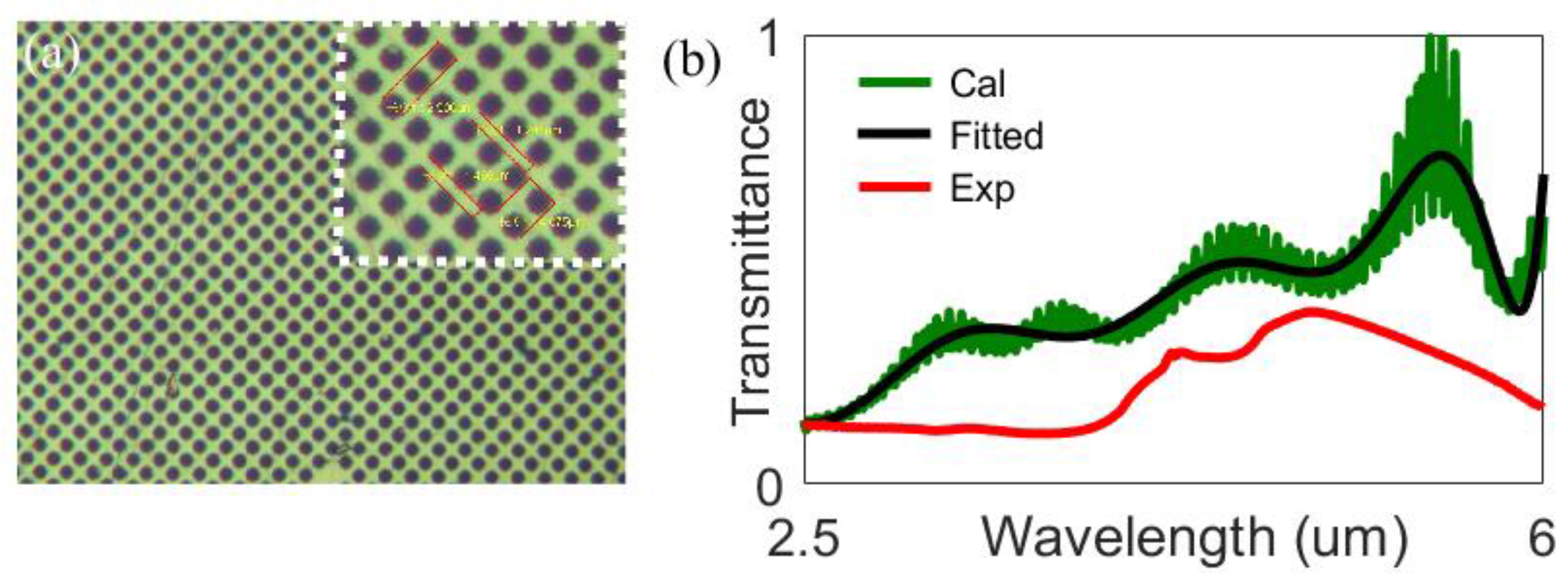
As shown in Figure 7a, a periodic subwavelength metal film filter based on hollow circle hole is designed and manufactured. Owing to the radius of the circle hole being too small, it is difficult to control the exposure time in the manufacturing process. It can be seen from the enlarged part in the figure that the radius of the circle hole is reduced after the photoresist is exposed, whereby the excess of the UV exposure time further reduces the radius of the circle hole after coating. Finally, the transmittance of the filter is smaller than that of the theoretical calculation. It should be noted that the positions of the transmission peaks are basically the same.
4. Conclusions
Through CST microwave studio, the transmission characteristics of the light in the visible light and infrared band are studied. Based on the two port transmission line theory, the multi cascade calculation and direct simulation of different materials and their thicknesses are carried out. The results show that when the structure contains only transparent substrate materials or only metal materials, the transmission characteristics obtained by direct simulation and cascade calculation are completely consistent. Ulteriorly, when the structure is cascaded by a single layer of metal material and a single layer of transparent substrate material, there is a slight difference between the results of direct simulation and cascade calculation, and the difference in transmittance at the same frequency is about 0.15. To summarize, the comparative study of direct simulation and cascade calculation between different types and thicknesses of materials presents an important reference value for solving problems such as the large thickness transparent substrate in micro/nano lithography technology, which cannot be directly simulated, or the overlong simulation time. On the other hand, a periodic subwavelength metal film filter based on circle hole array is designed and manufactured, and its analysis method accuracy of two port transmission line cascading calculation is verified by comparison. At the same time, a frequency selective optical element whose response band is concentrated in 3.8–4.7 um is realized.
Author Contributions
Conceptualization, K.W., P.L. and X.H.; data curation, K.W.; methodology, K.W.; software, K.W., Y.L., W.L. and Y.X.; project administration, Y.X., P.L. and X.H.; supervision, X.H.; writing—original draft, K.W.; writing—review, X.H.; data analysis, K.W. All authors have read and agreed to the published version of the manuscript.
Funding
This work is supported by the Foundation of Hunan Talents (2020RC3028), the Science Foundation of Hunan Province (2022JJ20045).
Institutional Review Board Statement
Not applicable.
Informed Consent Statement
Not applicable.
Data Availability Statement
Not applicable.
Conflicts of Interest
The authors declare no conflict of interest.
References
- Zhao, J.; Song, J.; Xu, T.; Yang, T.; Zhou, J. Controllable linear asymmetric transmission and perfect polarization conversion in a terahertz hybrid metal-graphene metasurface. Opt. Express 2019, 27, 9773–9781. [Google Scholar] [CrossRef] [PubMed]
- Feng, H.; Wang, L. Surface plasmon resonance sensor working at terahertz frequency. Spectrosc. Spectr. 2011, 31, 2017–2020. [Google Scholar]
- Xie, H.; Pan, Y.; Fedder, G. A CMOS-MEMS mirror with curled-hinge comb drives. J. Microelectromech. Syst. 2003, 12, 450–457. [Google Scholar]
- Bernstein, J.; Miller, R.; Kelley, W.; Ward, P. Low-noise MEMS vibration sensor for geophysical applications. J. Microelectromech. Syst. 2002, 8, 433–438. [Google Scholar] [CrossRef]
- Wang, F.; Cheng, R.; Li, X. MEMS vertical probe cards with ultra densely arrayed metal probes for wafer-level IC testing. J. Microelectromech. Syst. 2009, 18, 933–941. [Google Scholar] [CrossRef]
- Jang, J.; Javidi, B. Improved viewing resolution of three-dimensional integral imaging by use of nonstationary micro-optics. Opt. Lett. 2002, 27, 324–326. [Google Scholar] [CrossRef] [PubMed]
- Nikolajeff, F.; Karlsson, M. Diamond micro-optics: Microlenses and antireflection structured surfaces for the infrared spectral region. Opt. Express 2003, 11, 502–507. [Google Scholar]
- Xu, H.; Yu, C.; Wang, S.; Viktor, M.; Xie, T.; Rogers, J. Deformable, programmable, and shape-memorizing micro-optics. Adv. Funct. Mater. 2013, 23, 3299–3306. [Google Scholar] [CrossRef]
- Pregibon, D.; Toner, M.; Doyle, P. Multifunctional encoded particles for high-throughput biomolecule analysis. Science 2007, 315, 1393–1396. [Google Scholar] [CrossRef] [Green Version]
- Song, S.; Kim, K.; Choi, S.; Han, S.; Lee, H.; Kwon, S.; Park, W. Fine-tuned grayscale optofluidic maskless lithography for three-dimensional freeform shape microstructure fabrication. Opt. Lett. 2014, 39, 5162–5165. [Google Scholar] [CrossRef]
- Dendukuri, D.; Pregibon, D.; Collins, J.; Hatton, T.; Doyle, P. Continuous-flow lithography for high-throughput microparticle synthesis. Nat. Mater. 2006, 5, 365–369. [Google Scholar] [CrossRef]
- Wen, K.; Zhang, Z.; Jiang, X.; He, J.; Yang, J. Image representation of structural color based on edge detection algorithm. Results Phys. 2020, 19, 103440–103447. [Google Scholar] [CrossRef]
- Wen, K.; Zhang, Z.; Jiang, X.; He, J.; Yang, J. Plasmonics induced multifunction optical device via hoof-shaped subwavelength structure. Appl. Sci. 2020, 10, 2713. [Google Scholar] [CrossRef]
- Filippo, C.; Agostino, M.; Giuliano, M. Efficient analysis of frequency-selective surfaces by a simple equivalent-circuit model. IEEE Antennas Propag. Mag. 2012, 54, 35–48. [Google Scholar]
- Zhang, S.; Ren, Y.; Cai, H.; Chen, X.; Qu, G.; Xin, M. Research on transmission spectra of mid infrared metal micro nano structure. Opt. Tech. 2022, 48, 177–183. [Google Scholar]
- Romanini, D.; Kachanov, A.; Sadeghi, N.; Stoeckel, F. CW cavity ring down spectroscopy. Chem. Phys. Lett. 1997, 264, 316–322. [Google Scholar] [CrossRef]
- Wen, K.; Luo, X.; Chen, Z.; Zhu, W.; Guo, W.; Wang, X. Enhanced optical transmission assisted near-infrared plasmonic optical filter via hybrid subwavelength structures. Plasmonics 2019, 14, 1649–1657. [Google Scholar] [CrossRef]
- Padooru, Y.; Yakovlev, A.; Kaipa, C. Dual capacitive-inductive nature of periodic graphene patches: Transmission characteristics at low-terahertz frequencies. Phys. Rev. B 2013, 87, 115401–115410. [Google Scholar] [CrossRef]
- Luukkonen, O.; Simovski, C.; Granet, G. Simple and accurate analytical model of planar grids and high-impedance surfaces comprising metal strips or patches. IEEE Trans. Antennas Propag. 2008, 56, 1624–1632. [Google Scholar] [CrossRef] [Green Version]
- Huang, X.; Zhang, X.; Hu, Z.; Aqeeli, M.; Alburaikan, A. Design of broadband and tunable terahertz absorbers based on graphene metasurface: Equivalent circuit model approach. IET Microw. Antennas Propag. 2015, 9, 307–312. [Google Scholar] [CrossRef]
- Cheng, C.; Chen, J.; Shi, D.J.; Wu, Q.Y.; Ren, F.F.; Xu, J.; Fan, Y.X.; Ding, J.P.; Wang, H.T. Physical mechanism of extraordinary electromagnetic transmission in dual-metallic grating structures. Phys. Rev. B 2008, 78, 075406–075415. [Google Scholar] [CrossRef]
- Suckling, J.R.; Hibbins, A.P.; Lockyear, M.J.; Preist, T.W.; Sambles, J.R.; Lawrence, C.R. Finite conductance governs the resonance transmission of thin metal slits at microwave frequencies. Phys. Rev. Lett. 2004, 92, 147401–147404. [Google Scholar] [CrossRef] [PubMed]
- Sambles, J.R.; Bradbery, G.W.; Yang, F. Optical excitation of surface plasmons: An introduction. Contemp. Phys. 1991, 32, 173–183. [Google Scholar] [CrossRef]
Figure 1.
Unit structure diagram and structure diagram under different cascading conditions. (a) Multiple layers of different materials; (b) Single transparent material; (c) Single metallic materials; (d) Single-layer metal materials and transparent materials.
Figure 1.
Unit structure diagram and structure diagram under different cascading conditions. (a) Multiple layers of different materials; (b) Single transparent material; (c) Single metallic materials; (d) Single-layer metal materials and transparent materials.
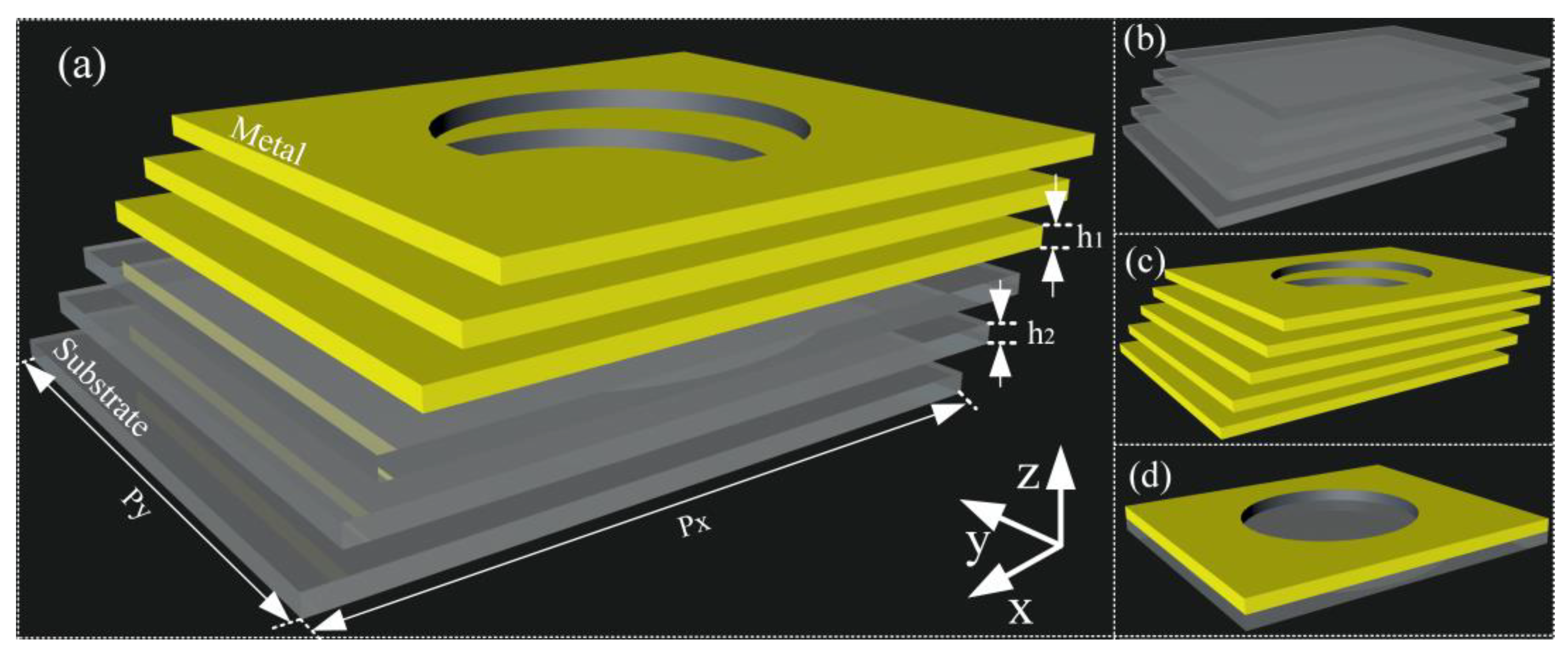
Figure 2.
Cascade response when only transparent substrate is contained on 60–100 THz band, wherein the black curve is the case with a thickness of 0.1 um, that is, the cascade benchmark. (a) Al2O3; (b) SiO2; (c) Si.
Figure 2.
Cascade response when only transparent substrate is contained on 60–100 THz band, wherein the black curve is the case with a thickness of 0.1 um, that is, the cascade benchmark. (a) Al2O3; (b) SiO2; (c) Si.
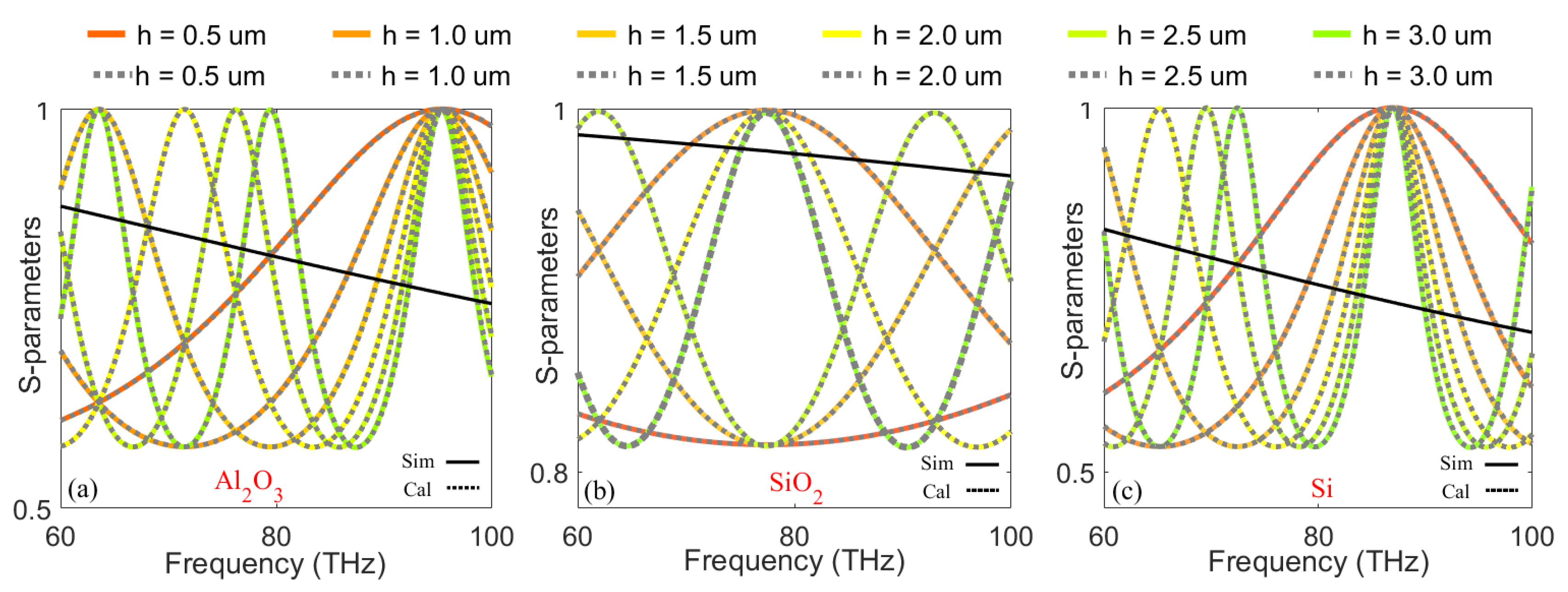
Figure 3.
Cascade response when only metallic film is contained on 60–100 THz band, wherein the black curve is the case with a thickness of 0.1 um, that is, the cascade benchmark. (a) Au; (b) Ag; (c) Al.
Figure 3.
Cascade response when only metallic film is contained on 60–100 THz band, wherein the black curve is the case with a thickness of 0.1 um, that is, the cascade benchmark. (a) Au; (b) Ag; (c) Al.
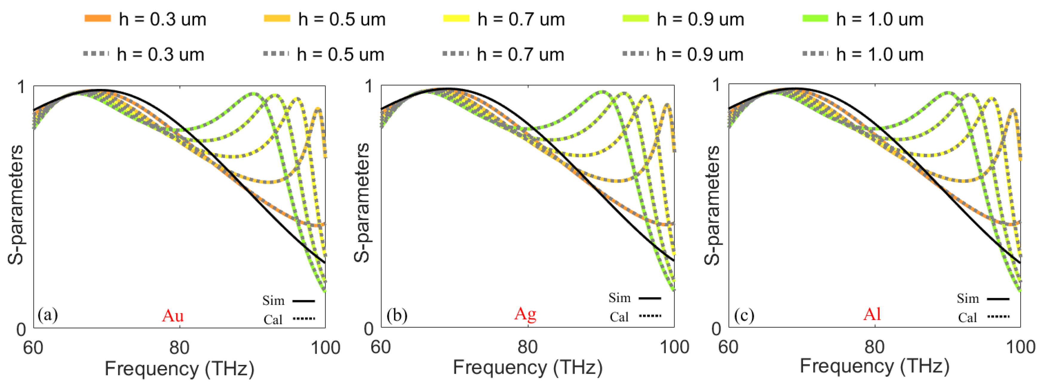
Figure 4.
Cascade response when only transparent substrate is contained on 120–750 THz band. The black curve is the case with a thickness of 0.1 um, that is, the cascade benchmark. (a) Al2O3; (b) SiO2; (c) Si.
Figure 4.
Cascade response when only transparent substrate is contained on 120–750 THz band. The black curve is the case with a thickness of 0.1 um, that is, the cascade benchmark. (a) Al2O3; (b) SiO2; (c) Si.
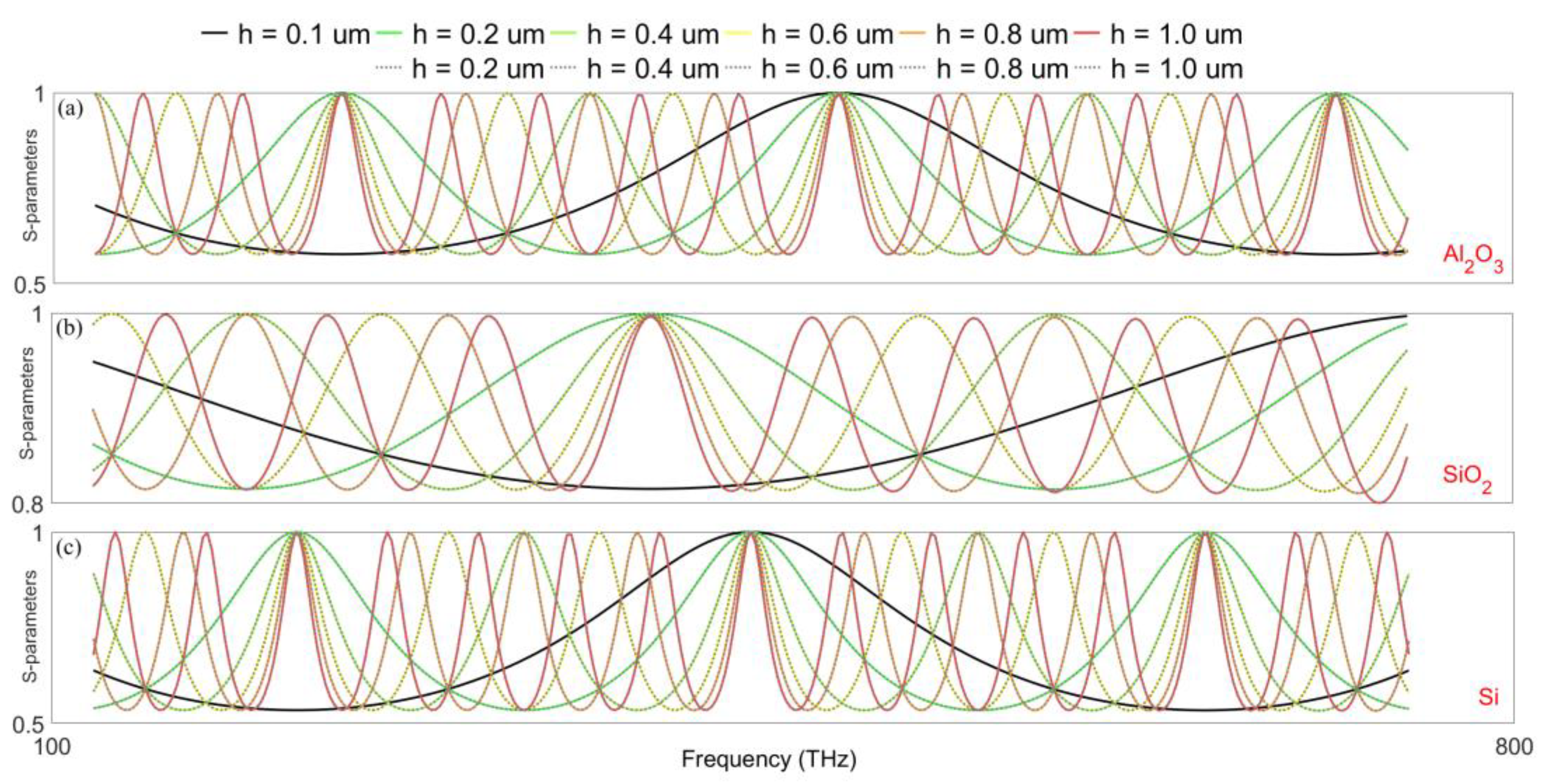
Figure 5.
Cascade response when only containing metallic film (Au) on 120–750 THz band, wherein the black curve is the case with a thickness of 0.1 um, that is, the cascade benchmark.
Figure 5.
Cascade response when only containing metallic film (Au) on 120–750 THz band, wherein the black curve is the case with a thickness of 0.1 um, that is, the cascade benchmark.

Figure 6.
Cascade response of multiple mixed cascade responses of the transparent substrate and the metal film. Among them, the black dot line graph is the 8th degree polynomial fitting of the simulation results. (a) The thickness is 0.1 um (single layer); (b) The thickness is 1 um (ten layers).
Figure 6.
Cascade response of multiple mixed cascade responses of the transparent substrate and the metal film. Among them, the black dot line graph is the 8th degree polynomial fitting of the simulation results. (a) The thickness is 0.1 um (single layer); (b) The thickness is 1 um (ten layers).

Figure 7.
(a) SEM image with the periodically arranged micro/nano structure and the partial enlarged view. (b) The transmission spectrogram. Among them, the green curve is the case of cascade computing; the black curve is the result of 10th degree polynomial fitting for the cascade calculation; and the red curve is the actual measurement result.
Disclaimer/Publisher’s Note: The statements, opinions and data contained in all publications are solely those of the individual author(s) and contributor(s) and not of MDPI and/or the editor(s). MDPI and/or the editor(s) disclaim responsibility for any injury to people or property resulting from any ideas, methods, instructions or products referred to in the content. |
© 2023 by the authors. Licensee MDPI, Basel, Switzerland. This article is an open access article distributed under the terms and conditions of the Creative Commons Attribution (CC BY) license (https://creativecommons.org/licenses/by/4.0/).
Share and Cite
MDPI and ACS Style
Wen, K.; Huang, X.; Liang, Y.; Liu, W.; Xu, Y.; Liu, P. Cascade Analysis Method of Multilayer Optical Films Structure Based on Two Port Transmission Line Theory. Appl. Sci. 2023, 13, 1337. https://doi.org/10.3390/app13031337
AMA Style
Wen K, Huang X, Liang Y, Liu W, Xu Y, Liu P. Cascade Analysis Method of Multilayer Optical Films Structure Based on Two Port Transmission Line Theory. Applied Sciences. 2023; 13(3):1337. https://doi.org/10.3390/app13031337
Chicago/Turabian StyleWen, Kui, Xianjun Huang, Yuanlong Liang, Wencong Liu, Yanlin Xu, and Peiguo Liu. 2023. "Cascade Analysis Method of Multilayer Optical Films Structure Based on Two Port Transmission Line Theory" Applied Sciences 13, no. 3: 1337. https://doi.org/10.3390/app13031337
Note that from the first issue of 2016, this journal uses article numbers instead of page numbers. See further details here.