
Advances in High–Speed, High–Power Photodiodes: From Fundamentals to Applications

1
Fabulas Laboratory, Department of Electrical Engineering, Polytechnique Montreal, Montreal, QC H3T 1J4, Canada
2
Fabulas Laboratory, Poly–Grames Research Center, Polytechnique Montreal, Montreal, QC H3T 1J4, Canada
3
Department of Electrical and Computer Engineering, Concordia University, Montreal, QC H3G 1M8, Canada
4
Blue Origin LLC, Kent, WA 98032, USA
5
Fabulas Laboratory, Department of Engineering Physics, Polytechnique Montreal, Montreal, QC H3T 1J4, Canada
*
Authors to whom correspondence should be addressed.
Appl. Sci. 2024, 14(8), 3410; https://doi.org/10.3390/app14083410
Submission received: 29 February 2024
/
Revised: 22 March 2024
/
Accepted: 25 March 2024
/
Published: 17 April 2024
(This article belongs to the Special Issue Advanced Optical-Fiber-Related Technologies)
Abstract
:High–speed, high–power photodiodes play a key role in wireless communication systems for the generation of millimeter wave (MMW) and terahertz (THz) waves based on photonics–based techniques. Uni–traveling–photodiode (UTC–PD) is an excellent candidate, not only meeting the above–mentioned requirements of broadband (3 GHz~1 THz) and high–frequency operation, but also exhibiting the high output power over mW–level at the 300 GHz band. This paper reviews the fundamentals of high–speed, high–power photodiodes, mirror–reflected photodiodes, microstructure photodiodes, photodiode–integrated devices, the related equivalent circuits, and design considerations. Those characteristics of photodiodes and the related photonic–based devices are analyzed and reviewed with comparisons in detail, which provides a new path for these devices with applications in short–range wireless communications in 6G and beyond.
1. Introduction
High data rate and high–quality transmission, large–capacity data storage, wireless short–range links, sensing, and imaging bring new challenges for current communication systems. Parts of the of microwave (MW), millimeter wave (MMW), and terahertz (THz) bands, which cover the frequency from 20 GHz to 3 THz, as shown in Figure 1, provide an appropriate choice for the above–mentioned challenges [1,2,3,4]. The exciting MMW and THz bands (20 GHz~1 THz), which are located between the radio waves and light waves, combine both their qualities and advantages, including large available bandwidth, high information capacity, transparent for some kinds of materials, high–spatial resolution, smaller beam scattering than infrared and visible light, and greater safety for the human body than x–rays and gamma rays [5,6,7]. Based on the above–mentioned advantages of the frequency band, it would bring about many potential applications [7], such as high–capacity wireless links, short–range wireless communication systems, and inspection system, high–resolution imaging transmission, spectroscopy, remote gas sensing and detection, security system and astronomical radio telescope system. More–over, this frequency band would support 6G technology for a high data rate (100~100 Gbit/s), helping towards a fully connected world in the future.
However, the large atmospheric attenuation (Figure 1) [8,9] in wireless communication systems needs to be considered (i.e., the attenuation caused by the rain and fog, free–space propagation loss (FSPL), gas loss, and signal loss from fiber to chip [8,9,10,11]) with the exception of focusing on the two key figures, i.e., the data rates or information capacity and transmission distance. To compensate for the FSPL limitation, high–gain and high–output power antennas or phased array antennas for beam forming/beam steering [12,13] should be considered for both transmitter and receiver systems. For the transmitter in communication systems, using large–scale photonic integrated circuit (PIC) techniques has an unparalleled impact on the continually reducing footprint, coupling loss, low power consumption and cost, while gradually increasing stability, reliability, and functionality [14]. Photonics–based technology is not only used for the development of MMW to THz communication techniques in systems with lower loss in optical fibers, large bandwidth, and miniaturized device/system [6,7,8,9,15,16,17,18,19,20,21,22,23,24,25] but it can also reduce some drawbacks which are brought forth by electronics–based technology, including high propagation loss in coaxial cables, narrow bandwidth, incompatibility with system operations at high–frequency bands and bulky feeding methods [26,27,28,29].
In this scheme, photonic–based techniques are derived from optical to RF signal conversions utilizing the photomixing method [30]. Since there is an output power limitation using a single photomixer, the InP–based semiconductor devices have been employed and led by a uni–traveling–carrier photodetector (UTC–PD) [31,32], operating at a long fiber–optics communication band (1.31~1.55 μm), which can be used to further enhance the output power up to a mW level around 300 GHz [9]. However, the new requirements of high data rate transmission in future 6G poses another challenge for THz systems. In addition, due to the lack of appropriate power amplifiers in the THz system transmitting terminally along with the difficulty of miniaturizing the monolithically integrated system employing Si–lens, the combination of high–speed, high–power UTC–PD (or UTC–PD array) and high–gain, high–output power antenna and/or arrays would be a better choice to tackle the power limitation problem. Furthermore, the optical–to–electrical (O/E) conversion efficiency and heat dissipation at a high bias voltage also needs to be considered. We could use resonant cavity enhanced (RCE) structure [33] employing distributed Bragg reflector (DBR) [34], subwavelength grating (SWG) mirrors [35] as bottom reflectors and dielectric layers as top reflectors to increase O/E conversion efficiency, while using high conductivity AlN [36,37], diamond [38] or SiC [39] substrates to reduce heat dissipation. Moreover, the slow light effect resulting from Bragg grating structures [40,41] with a remarkably low group velocity might offer a possible and promising solution to successfully compress optical signals and enhance light–matter interactions, and the enhanced O/E conversion efficiency in PDs could be possible while the joule heat problem at a higher bias voltage, device footprint reduction, and low power consumption could also be solved in the future.
This review work is structured as follows. Section 2 presents the overall design considerations for photodiodes (PDs), including the principles of PIN–PD and UTC–PD, 3–dB bandwidth analysis and discussion, equivalent circuit models, and saturation current and RF output power. Section 3 shows the solutions of bandwidth–responsivity trade–off, which are integrated or quasi–integrated with high–reflected mirrors for III–V and group–IV photodiodes, and microstructure photodiodes with microholes for enhancing light–matter interactions. Section 4 narrates the photodiode photonic–integrated applications, which relate to the photodiodes integrated with short stubs for output power improvement as well as the integrations with planar antennas for transmitters/emitters from MMW to THz bands. The discussion and conclusions are given in Section 5 and Section 6.
2. Overall Design Considerations for Photodiodes
2.1. Principles of PIN–PD and UTC–PD
The band diagrams for PIN–PD [42,43] and UTC–PD [5,31,32,44,45] are shown in Figure 2. PIN–PD has a simple three–layer structure, i.e., wide–bandgap P– and N–layers, and a depleted absorber. Both holes and electrons in the depleted absorber of PIN–PD contribute to the response, but the output response mainly depends on the low–velocity carrier holes, whose transport velocity is an order of magnitude lower than that of electrons, which limits the photoresponse to some extent.
The UTC–PD band structure, by dividing the PIN–PD absorber into two layers, is composed of a p–type neutral absorber and a wide–bandgap (depleted) carrier collector [31,32]. By employing a bandgap grading or/and doping grading in the absorber, the quasi–field is formed to reduce the electron traveling time effectively. In the meantime, the photogenerated majority holes in the InGaAs absorber respond quickly within several picoseconds due to the high concentration of electrons, leading to a negligible effect on the photoresponse; therefore, the high–velocity electrons dominate the photoresponse of UTC–PDs. Furthermore, the velocity of electrons () is usually 6~10 bigger than that of holes () [5], together with the quasi–ballistic transport (overshoot velocity) [46] in the InP collector, which leads to a quite short total delay time in the whole UTC–PD. For PIN–PD and UTC–PD with the same absorber (), the UTC–PD () represents a superior frequency response with a shorter traveling time in the collector due to the large difference in carrier velocities, though the carriers in UTC–PD travels ~three times the average distance than that in PIN–PD [44].
During high optical input, the charge intensity increases together with the increasing photocurrent in the depletion, producing a space charge effect due to the charge accumulation, while the field and potential profiles are modulated resulting in output saturation and a nonlinear response. For PIN–PD, as shown in Figure 2a, the charge storage happens at high injection conditions, resulting in the band bending and field screening, which finally causes output current saturation. However, in UTC–PD, shown in Figure 2b, only electrons participate in the space charge effect, whose velocity overshoot, even facing the decreased electrical field. Finally, the saturation occurs because of the current blocking produced from the heterojunction interface between the absorber and collector; while this state will be slower than that in PIN–PD, it is because UTC–PD can withstand a charge density an order of magnitude higher than PIN–PD [5,44]. In addition, the space charge in UTC–PD can not only be compensated by doping the spacer layer at the absorber/collector (InGaAs/InP) heterojunction interface but also can be reduced by employing a heavily n–doped InP charge (cliff) layer to increase the electrical field of the spacer layer [47]. Therefore, UTC–PD is a typical representative of high–speed response and high–output current.
In a typical UTC–PD structure, the bandgap discontinuity (the abrupt conduction band barrier) at the InGaAs absorber and InP collector interface causes the current blocking effect, thus leading to the device output current saturation. To smooth this discontinuity and suppress the blocking effect, the compositional graded quaternary system material (for spacer layers) is usually employed to improve device performance [48]. Therefore, the design of lattice–matched to InP [49] must be considered, while the cutoff wavelength–related refractive index and permittivity is shown in Figure 3a. However, the introduction of quaternary system material (Figure 3b) might bring certain difficulties for epitaxial growth and the device fabrication process. Therefore, a dipole–doped regime, as shown in Figure 3b is incorporated to reduce the conduction band barrier, which uses a lower dipole–doping concentration ( to avoid out–diffusion) to fully suppress the conduction band offset only left with a spike–like barrier for electrons to tunnel through [50,51,52].
2.2. 3–dB Bandwidth Analysis and Discussion
Response time is a physical quantity that characterizes how quickly a PD responds to an incident light signal, that is, it represents the total time it takes for a PD to convert an optical signal into an electrical signal.
The total response time of PD generally consists of three parts: (a) diffusion time of electrons in the absorption layer, , (b) circuit time constant, , determined by junction capacitance and load resistance, and (c) drift time of electrons in the collection layer, [44]. PIN–PD is usually made up of parts (a) and (b), while (c) belongs to UTC–PD [44,53,54]. Therefore, the total response time for general UTC–PD can be given as
while the PIN–PD can be dealt with as a special case, just having a single intrinsic/depletion layer, . The RC–delay time–limited bandwidth, , and transit–time–limited bandwidth, , usually consist of the main 3–dB bandwidth of a PD, which here the diffusion is neglected at the high–frequency response. We assume that a PD has one single intrinsic layer (Figure 4) with the i–layer thickness of and the area of , so the can be expressed as
where the junction capacitance approximately equals PD capacitance (in ideal cases), the ε is the relative permittivity of i–layer, and R is the resistance and equals the sum of diode series resistance, , and the load resistance, , has a typical value of 50 Ω.
It needs to be noted that Equation (2) will be changed if a PD has multiple dielectric/depletion layers and the corresponding values will be replaced by the relative permittivity, , and the total depletion thickness, , respectively, which are shown as follows [55]:
and
Therefore, the total capacitance, and the RC–limited 3–dB bandwidth, can be rewritten as
and
where is the vacuum permittivity, with a value of .
For a UTC–PD with the same thickness of the absorber and collector, assuming a pure diffusion case without quasi–field, the 3–dB bandwidth can be given as [44,54]
where is the electron diffusion constant, is the thermionic velocity and the related equations and values are shown in Table 1.
In addition, for the electron drift/delay time–limited bandwidth in the collector of UTC–PD, , can be considered as
where the electron overshoot velocity in the InP collector is , while the corresponding electron drift time which is around 0.5~1 ps for a collector with a thickness of 200~400 nm. However, the electron drift time, , usually can be ignored for a designed UTC–PD which has a similar thickness for the absorber and collector due to the relatively greater carrier traveling time () in the absorber. The can be separately calculated to be 3.74 ps and 11.2 ps for the 200 nm and 600 nm absorber by [44,54]
It is quite clear that we can ignore the electron drift time when the thickness of the absorber approximately equals the collector.
Therefore, the total bandwidth, , as a general case, can be written as
while the similar values for the absorber and collector, i.e., , so Equation (10) can be changed to
and the also has another form, as shown in Equation (12), for treating PD with a small junction area less than 10 μm2.
For PIN–PD, both of the holes and electrons are in the single intrinsic/depletion layer, , while the hole and electron saturation velocity are and , so the 3–dB bandwidth for a PIN–PD with a thin absorber can be given as [43,54]
where the equals
, and the average velocity formula is . Meanwhile, a thinner absorber can make PIN–PD obtain a larger transit–time–limited bandwidth, but it also causes a decrease in the RC–limited bandwidth by Equation (2), while the drawback can be overcome in UTC–PD, just by independently designing the absorber and collector. Therefore, a thinner absorber can be used in UTC–PD for a larger transit–time–limited bandwidth without sacrificing the RC–limited bandwidth by well–designing a relatively thick collector. Additionally, some references show the detailed theoretical and experimental analysis of the characteristics for PIN–PD and UTC–PD, including energy band, electrical field, doping mechanism, optimization of absorber and collector, bandwidth, responsivity, saturation, and output power [56,57,58,59,60,61,62] as well as transient response [63], dark current [64,65], and P–contact shapes [66]. According to the above–mentioned bandwidth equations and the values from Table 1, the 3–dB bandwidths for PIN–PD and UTC–PD can be calculated as shown in Figure 5a, including the assumed values during the calculation.
It can be seen that the bandwidth of UTC–PD is proportional to [44,54] when the absorber thickness is larger than 100 nm, while it is proportional to for PIN–PD [44,54]. Figure 5c is from [44] as a reference. The well–designed UTC–PD has improved 3–dB bandwidths over 150 GHz, 220 GHz [70], while the maximum value is up to 310 GHz (Figure 5b), and the 10–dB and 15–dB bandwidths are separately 750 GHz and >1 THz, but the responsivity is only 0.07 A/W [67]. To improve the low responsivity of UTC–PD, the refracting–facet UTC–PD (RF–PD) [68] and total–reflection UTC–PD (TR–PD) [69] are proposed to increase the light propagation length in the absorber, where RF–PD uses an angled edge to reflect the light while TR–PD employs a V–grooved mirror integrated with two PD to totally reflect the back–illuminated light. A high responsivity of 1 A/W with 50 GHz 3–dB bandwidth (0.32 A/W and 170 GHz) is achieved for RF–PD, while the TR–PD shows 0.83 A/W responsivity and a 58 GHz 3–dB bandwidth, as shown in Figure 5d.
Up to now, many PIN–PD and UTC–PD structures are proposed to improve the device performance, including frequency response, output power, saturation current, and responsivity, while the common band diagrams, including simple p–i–n type (Figure 2a), partially depleted absorber (PDA) type, dual depletion type, general UTC type, hybrid absorber type, charge–compensated (CC) hybrid absorber type and near–ballistic (NB)/NB–CC type [31,32,38,44,47,71,72,73,74,75,76,77,78,79,80], are summarized and shown in Figure 6.
In practice for UTC–PD, we need to choose one of them for adequate design (such as device size, bandwidth, absorber and collector layers, doping, electrical field, electron mobility, diffusivity, and diffusion time, etc.) according to the requirements and applications. We take the UTC–PD design as an example and assume three types of p–doping in the absorber with the values of , , and , corresponding the electron mobility (μe) of 6000, 5000 and 4000 [44]. Using equations shown in Part 2.2, the electron traveling time in the absorber (), the electron drift time in the collector (), and the electron diffusion constant (i.e., electron diffusivity, ) can be calculated as given in Figure 7a–c and summarized in Figure 7d. From Figure 7d, we find that the is much bigger than and indicates the electron diffusion time in the absorber which determines the total carrier transit time [82], so it only needs to consider and use Equation (7), i.e., , to evaluate the device’s 3–dB bandwidth at MMW and THz frequency bands when the absorber thickness is smaller than 100 μm.
2.3. Equivalent Circuit Models
The time–delay equivalent circuit model for air–bridge type waveguide PIN–PD was thoroughly analyzed by Wang et al. [84,85,86], as shown in Figure 8. Fundamentally, a basic air–bridge typed–PD is a current generator, and the corresponding equivalent circuit is composed of four parts, as shown in Figure 9, including the PD itself, the air bridge, the coplanar waveguide (CPW), and the 50 Ω load [86,87]. The photocurrent can be obtained and simulated using a current source, , which is in parallel with the junction capacitance, , and the large junction shunt resistance (megohms, usually ), , and in series with a small series resistance, (or ) (related to , layers and ohmic contact resistance of metallic connection), as well as the air–bridge inductance from p–contact to p–electrode pad, (or ), determined by the bridge geometry. The is the capacitance between the air bridge and the n–electrode pad. The characteristic impedance, , of the CPW, which can be measured with open and short circuit yielding a p–electrode pad capacitance, and an n–electrode pad–induced pad inductance, (or ), is calculated by with a common value of (e.g., , , so in [87]). One thing to note is that some PDs do not use air bridge during the device fabrication process, so the parasitic capacitance between the p–electrode and n–electrode, and air–bridge inductance, (or ) could not be used in the equivalent circuit model, as shown in Figure 10.
To evaluate the opto–microwave conversion properties of high–speed PDs by using S–parameters (such as reflection coefficients S22 and optoelectronic conversion properties S21), a small–signal radio frequency (RF) equivalent circuit for PD is reported considering synthetically both the analysis of the carrier transit effect [88] and the external parasitic resistance–capacitance (RC) delay–time constant [85]. The small–signal RF equivalent circuit is shown in Figure 11, which uses the voltage (RF voltage, )–controlled current source (VCCS, , is denoted as transconductance representing optical–to–RF conversion quantum efficiency, i.e., responsivity) to replace of the current source, in Figure 9 and Figure 10, while the overall frequency response (O–E 3–dB bandwidth) of PD is determined by both of the transit time and the RC–delay time constant, i.e., . The transit–time bandwidth, of ac–photocurrent, is determined by the carrier transit–time effect (), which is indirectly affected by selecting the values of input circuit elements of , , and . The signal source impedance is . The RC–delay time constant bandwidth can be calculated using Equation (6). In addition, the elements in an external circuit, such as in the air bridge, CPW pad (and P–contact shapes [66]), and load, also have an effect on the overall frequency response of PDs.
The similar and/or improved equivalent circuit models and RF small–signal equivalent circuit models, which are given from some specific examples for both PIN–PD and UTC–PD, with and without air bridge, can be found in previous works [25,85,86,87,89,90,91,92,93,94,95,96,97,98,99,100,101,102,103,104,105,106,107,108,109,110,111,112,113,114,115,116,117,118,119]. Some typical improved RC–delay time models are the modified UTC–PD (MUTC−PD) (Figure 12a) [89] and the dipole–doped UTC–PD (Figure 12b) [50], which are exploited as follows. For the MUTC–PD [89] (Figure 12a) and dual–drifting layer UTC–PD (DDL–UTC–PD) [100], Li et al. focus on the analysis of the absorbing depleted region (resistance, , and capacitance, ) and the non–absorbing depleted region (resistance, , and capacitance, ). Based on the RF small–signal equivalent circuit model without considering the air–bridge circuit, as shown in Figure 13a, the improved equivalent circuit model of the RC–delay time is shown in Figure 13b, while the further simplified one without considering and is reported by Han et al. [90], as shown in Figure 13c. In the above–mentioned RC–delay time models, the bulk material resistance is , while represents P– and N–contact resistance, is the P–electrode parasitic capacitance. Based on this model, the experimental and circuit analysis exhibit the bandwidth of an MUTC–PD up to 40 GHz, while the affected factors of the device performance, such as space charge screening, self–induced electrical field and over–shoot effects, are also discussed in detail [89].
In particular, the dipole–doped structure [50], as shown in Figure 12b, has been proposed by Wang et al. to tackle the bandgap discontinuity between the InGaAs absorber and the InP collector interface, and also to simplify the difficulty of epitaxy growth. The corresponding equivalent circuit for the RC–delay time [96] proposed by Meng et al. is shown in Figure 13d, where the resistance and capacitance for the dipole–doped part are denoted as and . and represent the resistance of the absorber and collector, while the junction capacitance is . Through carefully choosing the values for circuit components, the simulated bandwidth matches the measured value very well from 10 MHz to 20 GHz and can be estimated to be ~62.5 GHz at a −5 V bias voltage.
To carefully analyze and depict UTC–PD impedance and photoresponse behavior, an accurate circuit model is proposed [99]. This model not only provides detailed explanations for inconsistent values at low frequencies (here, from DC to 30 GHz, the CPW parasitic effects are negligible) between the classical circuit models of PDs and measurements but even presents a comprehensive study for both the measured device impedance and S11 up to 110 GHz, while showing the values of frequency photoresponse up to 67 GHz. The RC–delay time of this new model is shown in Figure 13e, where two parallel circuits ( and ) are used to model the two spacers (or transition layers) in UTC–PD, while the parallel circuit denotes the carrier collector, and the represents the series resistance with a small value (related to , layers and ohmic contact resistance of metallic connection/doped materials). In addition, the heavily p–doped neutral thick absorber usually can be ignored due to a negligible resistive effect [99]. It is noted that the parasitic capacitance, , and inductance, of the CPW pad cannot be ignored if the designed device photoresponse is above 75 GHz. This model provides useful and accurate information to optimize the UTC–PD complex impedance over the frequency range, thus providing a method for power maximization from UTC–PD to an antenna and then radiating to the air, by employing complex conjugate impedance matching between them [99,120]. Based on this new accurate model, some UTC–PD structures are designed and integrated with antennas [22,25,121]. In Figure 14, the matching network is employed to optimize the impedance matching to increase the RF output power, while stray capacitance is introduced in model–2 (without in model–1) to represent the parasitic effect resulting from the flip–chip bonding [25]. Compared with Figure 14a, the accurate equivalent circuit model is used for UTC–PD in Figure 14b, and the extra capacitance is also employed [22].
Moreover, by optimizing the impedance transmission line of the signal pad in CPW, a new transmission line with a characteristic impedance of 96 Ω is introduced forming a new low–inductive peaking CPW [36,37,101]. Subsequently, the charge–compensated MUTC–PD (CC–MUTC–PD) [78] is flip–bonded with this new CPW on aluminum nitride (AlN) (or diamond submounts for thermal dissipation [38,122]) die for further increasing the bandwidth and decreasing the output power roll–off at >120 GHz frequency [121]. Similarly, an inductive 115 Ω characteristic impedance CPW, as shown in Figure 15, is proposed and fabricated to improve the PD bandwidth from 28 GHz to 37.5 GHz [90], while further optimization is applied for MUTC–PD to obtain higher 3–dB bandwidth (and RF output power) from 156 GHz (−0.16 dBm @ 170 GHz [111]) up to 220 GHz (−4.94 dBm @ 230 GHz [113]). Note that some special examples with detailed parameters have been reported in the above–mentioned literatures cited in this paper, so here they are not given.
2.4. Saturation Current and Output Power
High–power PDs with a broadband frequency response are key components serving as microwave photonic antenna systems [123,124,125], phased array antennas, MMW imaging and sensing systems [5], and analog fiber–optic links wireless communications [8,126,127,128,129]. The high–speed and high–power PD is a promising candidate, such as the UTC–PD which can be monolithically integrated with a matching circuit using a coplanar waveguide short stub to achieve saturation output power, obtaining a value of −13.2 dBm (20.8 mW) at 100 GHz with a −3 V bias voltage [90].
Furthermore, narrow bandwidth high–power also serves as an analog photonic emitter and oscillator systems. The charge–compensated MUTC–PD (CC–MUTC–PD) with a cliff layer [78] is an excellent candidate to achieve high power and high frequency which are realized by the flip–chip techniques on AlN [36,37] or diamond [38] submounts, as shown in Figure 16a, for thermal dissipation. Figure 16b shows that the dissipated power of the device bonded on the diamond submount is faster than that of the devices bonded both on AlN and no bonding. Similarly, the simulated results indicate that the lowest junction temperature is produced from the device bonded on the diamond submount when using the same input power, as shown in Figure 16c.
Considering to use the well–designed high impedance CPW signal transmission line, bonding on AlN submount, a 9 μm CC–MUTC–PD with 70 GHz bandwidth achieves an RF output power of −2.6 dBm at 160 GHz [121]. To further improve the RF output power, high thermal conductivity substrates, including AlN and diamond, are employed bonding with CC–MUTC–PDs using flip–chip techniques [114], which shows 3–dB bandwidth of 105 GHz, 117 GHz, 129 GHz, and 150 GHz for PDs with diameters of 10 μm, 8 μm, 6 μm and 4 μm at a −3 V bias voltage, achieving an RF output power of −3 dBm at 150 GHz and −5.7 dBm at 165 GHz. Using the same methods for heat dissipation, the record RF output powers for gated modulation at 1 GHz and 10 GHz are separately 41.5 dBm (14.2 V) and 40 dBm (10 W) for 40 μm CC–MUTC–PD at a −36 V bias voltage [122], as shown in Figure 17.
In brief, the PD saturation current and RF output power is affected by several factors, including device area, PD types, bias voltage, fabrication quality, CPW design, junction heat with high–bias voltages, short microwave stub [131], submounts, measurements and so on, which need to be considered comprehensively. Furthermore, the superior conductivity of SiC substrate also is an excellent candidate for heat dissipation. Using the wafer–bonding technique, InP–based UTC–PD bonded on the SiC substrate [39] can increase the RF output power to a mW–level, i.e., 0.22 dBm (1.05 mW) at 300 GHz with 15.5 mA photocurrent and 2.01 dBm (1.59 mW) with the optimized bias at 18 mA photocurrent [132,133], while the output power is up to 4.04 dBm (2.53 mW) at 273 GHz with the optimized bias voltage at 18 mA photocurrent when this PD integrates with a taper slot antenna [134,135], as shown in Figure 18. The comparisons of 3–dB bandwidth, responsivity, saturation current or 1–dB compression saturation current and RF output power for different PDs [67,94,95,97,101,111,113,114,115,119,121,122,123,124,130,131,134,136,137,138,139,140,141,142,143,144,145,146,147,148,149,150,151,152] are shown in Table 2.
3. Solutions of Bandwidth–Responsivity Trade–Off
3.1. High–Reflected Mirrors for Photodiodes
High–performance PD based on III–V compound semiconductors serves as a key component and has already been demonstrated in various applications in wireless communications and radio–over–fiber and antenna systems [5]. The key parameters of PDs, which are responsivity, bandwidth, and saturation power, have been well designed for increasing one of them. For tackling the trade–off between bandwidth and responsivity in PD, several kinds of structures have been reported. The first structure is the resonant cavity enhanced (RCE) structure [33]. By selecting distributed Bragg reflectors (DBRs) as a bottom mirror in the PD, the incident light is reflected to the active layer, to achieve secondary absorption, as shown in Figure 19a. The detailed requirements for DBR design, which is also amenable to the RCE scheme, i.e., many number of different semiconductor material combinations, have been already reported in a review article [153].
Based on the reflection theory of RCE, many kinds of reflected mirror models, as shown in Figure 19b–f, which are used in vertical–mesa and waveguide types of PDs to improve the responsivity without sacrificing the bandwidth, have been proposed in the last 30 years. Most of the fabrication of reflected mirrors are the material combinations of DBRs (Figure 19b) [154,155,156,157,158,159,160,161,162,163,164,165], while periodic (or non–periodic) strip or concentric circular subwavelength gratings (SWGs), two–dimensional square bulk SWGs (Figure 19c) [140,161,166,167,168,169,170,171,172,173,174], Au mirrors [149], and even the scattering structure formed by a periodic cylindrical particle array [175], also can be employed as reflected ones. Those types of mirrors are usually either on the PD bottom (i.e., bottom mirrors) realized by direct epitaxial growth by metal–organic chemical vapor Deposition (MOCVD) or quasi–monolithically integrated using micron–level–thick benzocyclobutene (BCB) bonding (or integrated [69]) techniques, or on the top of the PD (i.e., top mirrors) implemented by employing the metal contacts (or strip gratings) by magnetic sputtering (or electron beam evaporation) or the flip–chip method with chemical etching [158,176,177,178].
Figure 20 shows PIN–PD and UTC–PDs integrated or quasi–integrated (BCB bonding) with two kinds of bottom mirrors [34,35,140,157,179] It can be seen from Figure 20a that the GaAs–based PIN–PD is integrated with 4 DBRs (three GaAs/AlGaAs DBRs and one Si/SiO2 DBRs) forming a four–mirror and three–cavity(M4C3) structure operating at 1550 nm [157]. The fabricated M4C3 structure achieves 70% peak quantum efficiency, 36 GHz 3–dB bandwidth, and quite a narrow spectrum linewidth (full–width at half–maximum (FWHM)) of 0.75 nm which is well–suited to high–density wavelength division multiplexing (WDM) communication systems [155]. The HR–UTC–PD [34], as shown in Figure 20b, is quasi–integrated with high–reflectivity (HR) DBR mirrors, which makes the responsivity increase by 23.2% without sacrificing the 3–dB bandwidth. As depicted in Figure 20c, the FR–UTC–PD [35] is quasi–integrated with a focusing reflection (FR) mirror, which is designed with a non–periodic concentric circular high–contrast grating (NP–CC–HCG) on the silicon substrate. Based on the 84.59% FR–efficiency, the integrated device achieves 36.5% improvement for the responsivity, without altering the 3–dB bandwidth. Figure 20d shows a symmetric–connected UTC–PD array (SC–PDA) integrated with a two–dimensional (2D) SWG beam–splitter [140], where the integrated device obtains an RF output power of 16 dBm at 12 GHz with a 87.9 mA saturation current and 0.438 A/W responsivity, showing stronger high–power handling capability than that of a single photodetector (~11 dBm@12 GHz and 46.7 mA, 0.179 A/W), without complex coupling, phase matching as well as any cooling techniques. Therefore, these kinds of mirrors perfectly realize the decoupling between the responsivity and bandwidth for photodiodes, while the improvement of responsivity and/or bandwidth can be further enhanced if using the well–optimized bonding process in the future.
3.2. Microhole Design for Photodiodes
Moreover, the application of micro–holes [180,181,182,183,184,185] etched from the top until through the active regions is also an effective way to assist the light–matter interactions. Figure 21 shows PDs with different kinds of micro– or/and nano–holes in active layers for enhancing light–matter interactions to balance the frequency response and responsivity [180,184]. Figure 21(a1,a2) reports a novel design that uses the etched periodic or photon–trapping micro– and nanoholes (600~1700 nm diameters) with square (Figure 21(a3)) or hexagonal (Figure 21(a4)) shapes that penetrate from the top mesa to the bottom contact layer in the Si photodiode [180]. Such a structure reveals that the lateral propagating slow and stationary optical modes can be generated only using normal incident light, which promotes a well–rounded interaction of light with Si that is an order of magnitude greater compared with the same thick Si–film absorber while ensuring an ultrafast carrier transport. This design enables the Si–based PDs to monolithically integrate with CMOS and extends its applications for optical data links in data communications and computer networks [180].
Given the 1550 nm wavelength application, microstructure PIN–PD (MPIN–PD) is proposed and analyzed numerically by employing an InP substrate, as shown in Figure 21b [184]. The well–designed central obconical shape surrounded by a V–groove trench not only greatly facilitates the interaction of light and InGaAs absorber, but also increases the device responsivity and bandwidth simultaneously. With the optimized dimensions of the V–groove and center cone, together with the optimized circular electrodes, the efficiency and bandwidth of MPIN–PD are separately increased by 61% and 21%. In addition, the back–to–back type of PD [186], waveguide–coupled PD [187], dual–absorber PD [58,161,169] and near–ballistic PD [79] also can be used to achieve high responsivity.
With the evolution of the RCE scheme and tapered–holes structures, a novel model for vertical–mesa PD, as shown in Figure 19d, which is realized based on tapered holes and bottom mirrors, could be used to solve the trade–off between bandwidth and responsivity. For waveguide PDs, the responsivity could be improved by exploiting an SWG high–focused mirror which is made by periodic (or non–periodic) strip or concentric circular SWG bonded at the back of the device (Figure 19f), while the usage of DBR mirrors (Figure 19e) have already been simulated [188] and achieved experimentally [189] showing similar performance for the trade–off.
3.3. High–Reflected Mirrors for Group–IV Photodiodes
However, the PDs based on III–V compound semiconductors are not easy for CMOS compatibility, so the group–IV PDs are gradually paid more attention by researchers, which more easily enables electronic photonic integrated circuits (EPICs) with low–cost, compact, and large–scale integrations [190]. It is to be noticed that the Si–based PD cannot be directly used for the C–band and L–band fiber–optic telecommunication regimes due with the bandgap of 1.12 eV only resulting in a ~1107 nm cutoff wavelength.
Therefore, germanium (Ge) will play an important role for the above–mentioned telecommunication bands owing to a relatively small bandgap (less than 0.7 eV at room temperature), though its optical response rolls off rapidly beyond 1500 nm [191] while this defect can be solved by depositing the Ge–layer on the Ge–on–insulator (GOI) platform [190]. By introducing 0.16% tensile strain to the Ge active layer, the operation wavelength is extended to cover the entire range of telecommunication C– and L–bands (1530–1620 nm). The high refractive index Ge absorber with the low refractive indices of the bottom insulator and the deposited SiO2 top layer separately serve as two mirrors which finally constitute a RCE–Ge PD on the GOI platform [190] to increase the responsivity, similar to the model shown in Figure 19b. Such RCE–Ge PD on GOI (i.e., GOI–PD) indicates that the responsivity can be greatly increased up to 0.15 A/W at 1550 nm while covering the entire C– and L–bands due to the resonant cavity effect.
Meanwhile, germanium–tin (GeSn) PD on Si is another typical group–IV candidate for SWIR applications which only needs to incorporate Sn into Ge shrinking the direct bandgap and causing redshift of the absorption edge from C–band to the mid–infrared range and beyond [192,193]. GeSn–based (2.5% Sn) PIN–RCE–PD on SOI use the buried oxide (BOX) and the deposited SiO2 as the bottom and top mirrors forming multiple reflections to enhance light–matter interaction, which shows ~0.4 A/W responsivity at 0 V bias voltage in the C–band, which is much higher than that of the conventional GeSn PIN–PDs with the values of 0.1~0.3 A/W [194]. The introduction of 10% Sn extends the operation wavelength to a 2 μm band, where the metal–semiconductor–metal (MSM) RCE–GeSn–PD can work at 1550 nm and 2 μm wavelengths by optimizing the cavity length. Based on the RCE resonance effects, a record responsivity of 0.43 A/W is obtained with a −3 V bias voltage at 2 μm wavelength at room temperature, revealing that it is promising for CMOS–compatible photonic–integrated circuit applications covering the entire telecommunication bands in a 2 μm range [195].
4. Photodiode Photonic–Integrated Applications
4.1. Photodiodes Integrated with Short–Stubs
With the development of MMW to THz communication techniques, the photonics–based technology provides lower loss in the optical fiber and a large bandwidth while needing the PDs with a high output power and broadband high–frequency characteristics.
Furthermore, we could not ignore the connected compact rectangular waveguide (WR) output port for practical use in a package module [90,152,196,197,198,199,200]. Figure 22 shows two different equivalent circuits and the fabricated micrographs for the photonic MMW generator (PWG), where each PWG includes a UTC–PD, a short–stub matching circuit (impedance transformer), and a metal–insulator–metal (MIM) capacitor, (i.e., in Figure 22d,e) [196,199]. The calculated relative output power curves are given for comparisons as shown in Figure 22c, in which the higher power is obtained by PMG–A at ~100 GHz (W–band). Meanwhile, the PMG works at the J–band as shown in Figure 22f, where a WR–3 waveguide output port is used for practical use. It is noticed that a typical case is a coupler integrated with UTC–PD packaged with WR–1.5, which attains a record output power of −19 dBm at 500 GHz with a 9 mA photocurrent while showing a wide range 3–dB bandwidth of 340 GHz, i.e., from 470 GHz to 810 GHz [201]. The detailed results of PDs integrated with WR ports and short stubs [90,197,198,200,201] are shown in Table 3.
4.2. Photodiodes Integrated with Antennas
Another photonic–integrated device is PD with antennas for increasing output power for practical use. The general schematic diagram of the photonics–based transmitter and receiver is shown in Figure 23. One of the unique performances of UTC–PDs [44,54] is both a large bandwidth and high saturation output power, which can be used as an MMW signal emitter [123] for wireless applications.
To obtain V–band–to–G–band (50 GHz~220 GHz) photonically driven emitters and extend applications to MMW and THz signal wireless links, high–power photonic–integrated emitters with three types of planar antennas have been proposed [22,202], as shown in Figure 24. The high–speed and high–power broadband CC–MUTC–PD [78,101] with 0.2 A/W responsivity and 12 dBm output power is used for the MMW and THz emitter design. The fabricated emitter with the sinuous antenna and 8 μm PD shows a record output power of 20 dBm at 90 GHz with a photocurrent of 20 mA while achieving an output power of 9.9 dBm at 70 GHz, 11.5 dBm at 100 GHz, all with 7 mA photocurrent, for log–periodic and spiral antennas, respectively [22].
Using flip–chip technology, UTC–PD can be mounted on a planar slot antenna on the Si substrate [123,124,203], as shown in Figure 25a, and then boned on a hemispherical Si–lens to collimate the MMW signal direction, which generates a larger than 0.5 mW output power from the PD chip while radiating a bigger than 0.3 mW power into the free space, at a 120 GHz bandwidth [123,124]. Meanwhile, this design indicates the potential applications in future wireless communication, sensing, radar, measurement, and imaging systems based on photonic–assisted MMW generation and transmission techniques. Beyond the F–band, the electrical transmission line will bring loss and reflection, so the miniaturized PD–integrated antenna with a quasi–optical configuration (Figure 25b) is necessary for sub–MMW signal handling [204]. As shown in Figure 25c, a UTC–PD integrated with a log–periodic antenna achieves a saturation output power of 300 μW at a photocurrent of 20 mA (Figure 25d) [205]. Using a similar configuration, the UTC–PD integrated with a log–periodic antenna exhibits a high output power of 2.6 μW at 1.04 THz with a saturation current of 13 mA [204].
However, a single PD integrated with an antenna suffers some limitations, including the limited emitted power resulting from the saturation of PD and the limited antenna directivity due to the finite effective aperture of the planar antenna [206]. Here, four InP–based photodiodes operating at 300 GHz, which are integrated with a linear bowtie antenna array mounting on the Si–lens, are proposed, as shown in Figure 26, to increase the radiation power. Compared to the straight radiation of a single emitter, the array emitter realizes a 10.6 dB higher power (theoretical gain: 12 dB), while the 3–dB beamwidth is reduced by 8.5° and up to 22.5°, which achieves the output power increase and higher directivity. These photonic–integrated antenna arrays provide new solutions to wireless communications beyond 5G and will further exploit combinations of other photonic devices for application to future complex MMW and THz transceivers.
In addition, a resonant antenna integrated with UTC–PD is another excellent candidate to be employed for output power radiation in the THz bands [207,208,209]. Figure 27a shows the THz UTC–PD chip integrated with a twin–diploe antenna [209] using an impedance matching circuit [90] to enlarge the output power and the resonant behaviors are found exhibiting the peak output powers of 5.9, 3.8, and 1.1 μW at 0.78, 1.04 and 1.53 THz (Figure 27b), while generating a record output power of 10.9 μW at 1 THz with a photocurrent of 14 mA [209].
Moreover, the THz wave and THz beam steering provide great opportunities for free–space applications, including imaging, sensing, radar, and wireless communications in the 6G era and beyond [15,135,210]. Figure 27c shows a 4 × 1 UTC–PD array integrated with a 4×4 unidirectional slot antenna to generate THz signals based on coupled fiber beats techniques [211]. The adaptive genetic algorithm is used to control the produced THz beam steering and the experiment achieves a precise pointing towards the intended direction of the 300 GHz beam, which greatly improves the THz power efficiency by beam steering and paves the way for THz wireless communication using large–scale UTC–PD array [211,212,213].
Figure 27.
(a) THz UTC–PD chip integrated with twin–diploe antenna using impedance matching circuit and (b) the output power versus different frequency [209]. (c) Adaptive THz beam steering in fiber–coupled UTC–PD array chip to generate THz wave [211,212,213].

With the development of communication techniques, the frequency range (MMW to THz: 30 GHz~3 THz) between microwave and far–infrared is set to meet the growing demand. Exploiting and making the most of the MMW and THz wireless signals [7,214,215] with high–radiated power have long been studied and generated by the electronic system [26,27,28] or photonic system [6,8,9,15,16,17,18,19,20,21,22,23] or hybrid electronic–photonic systems [216,217], which have shown a very diverse range of application in information and communications, security screening, food and agriculture, biometrics, medical and medicine, drug inspection, semiconductor wafer inspection, and air pollution [218,219,220].
Given the photonic–generated THz signal, ultrafast broadband, and high–power PDs, such as UTC–PDs [44,54] and traveling–wave PD (TW–UTC–PD) [221], are necessary. By combining the TW–PD structure for high responsivity and the UTC–PD structure for high output power, a new TW–UTC–PD is proposed for integration with antennas for MMW and THz signal radiation [21,222]. The TW–UTC–PD separately integrates with the resonant, bowtie, and log–periodic antennas for generating THz signals, covering frequencies up to 1 THz. The radiated power at different photocurrent levels is shown in Figure 28, where the 4 × 15 μm2 PD integrated with a resonant antenna achieves an RF output power of 148 μW at 457 GHz and 24 μW at 914 GHz with a 10 mA photocurrent (Figure 28a). Figure 28b shows that the RF output power of 105 μW at 255 GHz and 10 μW at 612 GHz with a 13 mA photocurrent are attained by a 2.5 × 50μm2 PD integrated with a bowtie antenna while exhibiting 70 μW at 150 GHz with a 9 mA photocurrent for integrating with a log–periodic antenna.
Another type of PD for THz applications is related to the design, usage, and optimization of the hybrid absorber UTC–PD (i.e., modified UTC–PD, MUTC–PD) [72], as shown in Figure 29. The band diagram for this type of MUTC–PD is shown in Figure 29a, where the absorber consists of a non–depleted absorber with p–doping and a depleted absorber without doping. The maximum 3–dB bandwidth can be calculated while just comprehensively analyzing the numerical relation of thickness among depletion (), non–depleted (), and depleted () absorbers. Figure 29d shows the frequency response at different quasi–fields in the non–depleted absorber, while the and are separately 0.12 μm, 0.06 μm, and 0.18 μm. The 3–dB bandwidth is enlarged from 603 to 1087 GHz with the increase in quasi–field from 10 to 30 kV/cm.
The MUTC–PD is integrated with a bowtie antenna shown in Figure 29b, where Si–lens (Figure 29c) is employed to increase the output power. Being accompanied by a well–designed matching circuit and the rectangular waveguide output port, the quasi–optical antenna–integrated photomixer module can be completed as shown in the inset of Figure 29e. It can be seen that the measured output power gradually decreases with the increase in the frequency while the typical values are larger than −20 dBm at 300 GHz, −30 dBm at 1 THz, and approximately −40 dBm at 2 THz. Furthermore, the calculated results which changed with the different effective electron velocities are also shown in Figure 20e, as comparisons with the measured values. Parts of PDs photonic–integrated antennas [18,21,22,25,72,91,98,123,124,134,142,204,205,206,208,209,223,224,225,226,227] are summarized in Table 4.
5. Discussion
During the design of high–speed and high–output power photodiodes, the compatible photodiode–integrated devices, the measurement setups, and applications for communication systems, there are lots of considerations and challenges that need to be noticed. They are mainly reflected as follows: (1) The efficient optical coupling and precise alignment between the photodiode and other optical components. (2) The wider bandwidth with high response for photodiodes. (3) The wider dynamic range and linearity for higher output power without small saturation or signal distortion. (4) The effects resulting from temperature and heat from high–power conditions. (5) The reliability and robustness of photodiodes, and the scalability and modularity of photodiode–integrated devices. (6) The potential limitations at the 300 GHz band, such as the coverage range with high propagation loss, the penetrating obstacles from the walls, buildings, and vegetation, and the complexity and cost of exploiting and deploying photodiodes to the MMW and THz bands. (7) The design of corresponding other components matching with photodiodes in THz links and systems.
Though achieving high–speed, high–power photodiodes and photodiode–integrated devices with over 2 mW output power in the THz band has been realized, it is still a big challenge to apply photodiodes to 6G technology. Compared with existing communication systems, 6G requires ultra–high data rates (such as 200~1000 Gbit/s) and also requires the matching terahertz sources, photodiodes, and components in THz links and systems. However, considering the wider applications of photodiodes in transparent materials, including cell phone screens, smart windows, and automobile/aircraft win screens, is also a big challenge. A possible solution could be to implement the integration of photodiodes with waveguide–based Bragg grating devices in glass inscribed using femtosecond laser in the future.
6. Conclusions
This paper reviews the advances in high–speed, high–power photodiodes from fundamentals to applications. (1) For the overall design and consideration of photodiodes, this paper discusses the principles of PIN–PD and UTC–PD, while reporting the detailed calculation of the 3–dB bandwidth for the two typical photodiodes and summarizes the energy band diagrams for several kinds of photodiodes. Given the equivalent circuits, this paper shows the general ones and RF small–signal ones together, and also considers the different designs for the RC–delay time part and the external circuit parts, including the air bridge, CPW pad, and load. Additionally, the DC saturation and RF output power are also analyzed in detail and a table for comparison is also included. (2) The solutions of bandwidth–responsivity trade–off for photodiodes are discussed in detail, which range from the use of high–reflected mirrors to the making of microholes and extending the reflected mirrors for group–IV photodiodes. (3) The photodiode photonic–integrated applications are presented, including the integration with short stubs and various planar antennas for high output power at high–speed conditions, and showing the parameter comparisons in tables, which provides a reference for the practice use of photonics–based devices operating at the system–level with the radiation power up to the mW–level and beyond in the THz band.
Author Contributions
Conceptualization, Q.C.; methodology, software, Q.C.; validation, Q.C.; formal analysis, Q.C.; investigation, Q.C.; resources, Q.C.; data curation, Q.C.; writing—original draft preparation, Q.C.; writing—review and editing, Q.C. and X.Z.; visualization, Q.C.; supervision, X.Z., M.S.S. and R.K.; project administration, M.S.S. and R.K.; funding acquisition, M.S.S. and R.K. All authors have read and agreed to the published version of the manuscript.
Funding
This work was funded by the Natural Sciences and Engineering Research Council of Canada (NSERC), through the New Frontiers in Research Funding Fund (NFRF) with project number NFRFE–2020–00355.
Institutional Review Board Statement
Not applicable.
Informed Consent Statement
Not applicable.
Data Availability Statement
Not applicable.
Conflicts of Interest
Author Mohammad S. Sharawi was employed by the company Blue Origin LLC. The remaining authors declare that the research was conducted in the absence of any commercial or financial relationships that could be construed as a potential conflict of interest.
References
- Giordani, M.; Polese, M.; Mezzavilla, M.; Rangan, S.; Zorzi, M. Toward 6G Networks: Use Cases and Technologies. IEEE Commun. Mag. 2020, 58, 55–61. [Google Scholar] [CrossRef]
- Rajatheva, N.; Atzeni, I.; Bjornson, E.; Bourdoux, A.; Buzzi, S.; Dore, J.-B.; Erkucuk, S.; Fuentes, M.; Guan, K.; Hu, Y.; et al. White Paper on Broadband Connectivity in 6G. arXiv 2020, arXiv:2004.14247. [Google Scholar]
- Xiaohu, Y.; Cheng-xiang, W.; Jie, H.; Xiqi, G.; Michael, W.; Yongming, H.; Chuan, Z.; Yanxiang, J.; Min, Z.; Dongming, W.; et al. Towards 6G Wireless Communication Networks: Vision, Enabling Technologies, and New Paradigm Shifts. Sci. China Inf. Sci. 2020, 64, 110301. [Google Scholar]
- Koenig, S.; Lopez-Diaz, D.; Antes, J.; Boes, F.; Henneberger, R.; Leuther, A.; Tessmann, A.; Schmogrow, R.; Hillerkuss, D.; Palmer, R.; et al. Wireless Sub-THz Communication System with High Data Rate. Nat. Photonics 2013, 7, 977–981. [Google Scholar] [CrossRef]
- Nagatsuma, T.; Ito, H.; Ishibashi, T. High-Power RF Photodiodes and Their Applications. Laser Photonics Rev. 2009, 3, 123–137. [Google Scholar] [CrossRef]
- Renaud, C.C.; Natrella, M.; Graham, C.; Seddon, J.; Van Dijk, F.; Seeds, A.J. Antenna Integrated THz Uni-Traveling Carrier Photodiodes. IEEE J. Sel. Top. Quantum Electron. 2018, 24, 8500111. [Google Scholar] [CrossRef]
- Wakatsuki, A.; Muramoto, Y.; Ishibashi, T. Development of Terahertz-Wave Photomixer Module Using a Uni-Traveling-Carrier Photodiode. NTT Tech. Rev. 2012, 10, 1–7. [Google Scholar]
- Seeds, A.J.; Shams, H.; Fice, M.J.; Renaud, C.C. TeraHertz Photonics for Wireless Communications. J. Light. Technol. 2015, 33, 579–587. [Google Scholar] [CrossRef]
- Nagatsuma, T.; Ducournau, G.; Renaud, C.C. Advances in Terahertz Communications Accelerated by Photonics. Nat. Photonics 2016, 10, 371–379. [Google Scholar] [CrossRef]
- ITU. International Telecommunication Union ITU-R P.840-3: Attenuation Due to Clouds and Fog; ITU: Geneva, Switzerland, 1999. [Google Scholar]
- ITU. International Telecommunication Union ITU-R P.676-6: Attenuation by Atmospheric Gases; ITU: Geneva, Switzerland, 2005.
- Han, S.; Chih-Lin, I.; Xu, Z.; Rowell, C. Large-Scale Antenna Systems with Hybrid Analog and Digital Beamforming for Millimeter Wave 5G. IEEE Commun. Mag. 2015, 53, 186–194. [Google Scholar] [CrossRef]
- Omam, Z.R.; Abdel-wahab, W.M.; Gigoyan, S.; Safavi-naeini, S. High Gain 4 × 4 SIW Passive Phased Array Antenna. In Proceedings of the 2020 IEEE International Symposium on Antennas and Propagation and North American Radio Science Meeting, Toronto, ON, Canada, 5–10 July 2020; pp. 45–46. [Google Scholar]
- Nagarajan, R.; Member, S.; Joyner, C.H.; Schneider, R.P.; Bostak, J.S.; Butrie, T.; Dentai, A.G.; Dominic, V.G.; Evans, P.W.; Kato, M.; et al. Large-Scale Photonic Integrated Circuits. IEEE J. Sel. Top. Quantum Electron. Electron. 2005, 11, 50–65. [Google Scholar] [CrossRef]
- Song, H.J.; Nagatsuma, T. Present and Future of Terahertz Communications. IEEE Trans. Terahertz Sci. Technol. 2011, 1, 256–263. [Google Scholar] [CrossRef]
- Harter, T.; Ummethala, S.; Blaicher, M.; Muehlbrandt, S.; Wolf, S.; Weber, M.; Adib, M.M.H.; Kemal, J.N.; Merboldt, M.; Boes, F.; et al. Wireless THz Link with Optoelectronic Transmitter and Receiver. Optica 2019, 6, 1063–1070. [Google Scholar] [CrossRef]
- Bowers, S.M.; Abiri, B.; Aflatouni, F.; Hajimiri, A. A Compact Optically Driven Travelling-Wave Radiating Source. In Proceedings of the Optical Fiber Communication Conference 2014, San Francisco, CA, USA, 9–13 March 2014; pp. 18–20. [Google Scholar]
- Shi, J.-W.; Kuo, F.-M.; Wu, Y.-S.; Chen, N.-W.; Shih, P.-T.; Lin, C.-T.; Jiang, W., Jr.; Wong, E.-Z.; Chen, J.; Chi, S. A W-Band Photonic Transmitter-Mixer Based on High-Power Near-Ballistic Uni-Traveling-Carrier Photodiodes for BPSK and QPSK Data Transmission Under Bias Modulation. IEEE Photonics Technol. Lett. 2009, 21, 1039–1041. [Google Scholar] [CrossRef]
- Costanzo, R.; Yang, Z.; Beling, A.; Bowers, S.M. Wideband Balanced Photoreceivers with InP-Based Photodiodes and 65 Nm CMOS TIAs for Use in Optical Frequency Synthesis Systems. J. Light. Technol. 2019, 37, 5833–5839. [Google Scholar] [CrossRef]
- Ferguson, B.; Zhang, X.-C. Materials for Terahertz Science and Technology. Nat. Mater. 2002, 1, 26–33. [Google Scholar] [CrossRef] [PubMed]
- Rouvalis, E.; Renaud, C.C.; Moodie, D.G.; Robertson, M.J.; Seeds, A.J. Traveling-Wave Uni-Traveling Carrier Photodiodes for Continuous Wave THz Generation. Opt. Express 2010, 18, 11105–11110. [Google Scholar] [CrossRef] [PubMed]
- Shen, X.; Morgan, J.; Costanzo, R.; Sun, K.; Woodson, M.; Estrella, S.B.; Beling, A.; Bowers, S.M. High-Power V-Band-to-G-Band Photonically Driven Electromagnetic Emitters. IEEE Trans. Microw. Theory Tech. 2021, 69, 1474–1487. [Google Scholar] [CrossRef]
- Sun, K.; Beling, A. High-Speed Photodetectors for Microwave Photonics. Appl. Sci. 2019, 9, 623. [Google Scholar] [CrossRef]
- Nagatsuma, T.; Horiguchi, S.; Minamikata, Y.; Yoshimizu, Y.; Hisatake, S.; Kuwano, S.; Yoshimoto, N.; Terada, J.; Takahashi, H. Terahertz Wireless Communications Based on Photonics Technologies. Opt. Express 2013, 21, 23736. [Google Scholar] [CrossRef]
- Sun, K.; Moody, J.; Li, Q.; Bowers, S.M.; Beling, A. High Power Integrated Photonic W-Band Emitter. IEEE Trans. Microw. Theory Tech. 2018, 66, 1668–1677. [Google Scholar] [CrossRef]
- Assefzadeh, M.M.; Babakhani, A. Broadband Oscillator-Free THz Pulse Generation and Radiation Based on Direct Digital-to-Impulse Architecture. IEEE J. Solid-State Circuits 2017, 52, 2905–2919. [Google Scholar] [CrossRef]
- Wang, C.; Lu, B.; Lin, C.; Chen, Q.; Miao, L.; Deng, X.; Zhang, J. 0.34-Thz Wireless Link Based on High-Order Modulation for Future Wireless Local Area Network Applications. IEEE Trans. Terahertz Sci. Technol. 2014, 4, 75–85. [Google Scholar] [CrossRef]
- Razavian, S.; Babakhani, A. A THz Pulse Radiator Based on PIN Diode Reverse Recovery. In Proceedings of the 2019 IEEE BiCMOS and Compound semiconductor Integrated Circuits and Technology Symposium (BCICTS), Nashville, TN, USA, 3–6 November 2019; IEEE: New York, NY, USA, 2019; pp. 1–4. [Google Scholar]
- Deng, J.; Burasa, P.; Wu, K. Joint Multiband Linear Interferometric Receiver for Integrated Microwave and Terahertz Sensing and Communication Systems. IEEE Trans. Microw. Theory Tech. 2024, 1–13. [Google Scholar] [CrossRef]
- Ueda, A.; Noguchi, T.; Iwashita, H.; Sekimoto, Y.; Ishiguro, M.; Takano, S.; Nagatsuma, T.; Ito, H.; Hirata, A.; Ishibashi, T. W-Band Waveguide Photomixer Using a Uni-Traveling-Carrier Photodiode with 2-MW Output. IEEE Trans. Microw. Theory Tech. 2003, 51, 1455–1459. [Google Scholar] [CrossRef]
- Ishibashi, T.; Shimizu, N.; Kodama, S.; ITO, H.; Nagatuma, T.; Furuta, T. Uni-Traveling-Carrier Photodiodes. In Proceedings of the Ultrafast Electronics and Optoelectronics 1997, Incline Village, NA, USA, 17–21 March 1997; pp. 83–87.
- Ishibashi, T.; Ito, H. Uni-Traveling-Carrier Photodiodes. J. Appl. Phys. 2020, 127, 031101. [Google Scholar] [CrossRef]
- Kishino, K.; Unlu, M.S.; Chyi, J.-I.; Reed, J.; Arsenault, L.; Morkoc, H. Resonant Cavity-Enhanced (RCE) Photodetectors. IEEE J. Quantum Electron. 1991, 27, 2025–2034. [Google Scholar] [CrossRef]
- Chen, Q.; Huang, Y.; Zhang, X.; Duan, X.; Fei, J.; Ma, X.; Liu, T.; Wu, G.; Liu, K.; Ren, X. Uni-Traveling-Carrier Photodetector with High-Reflectivity DBR Mirrors. IEEE Photonics Technol. Lett. 2017, 29, 1203–1206. [Google Scholar] [CrossRef]
- Chen, Q.; Fang, W.; Huang, Y.; Duan, X.; Liu, K.; Sharawi, M.S.; Ren, X. Uni-Traveling-Carrier Photodetector with High-Contrast Grating Focusing-Reflection Mirrors. Appl. Phys. Express 2020, 13, 016503. [Google Scholar] [CrossRef]
- Zhou, Q.; Cross, A.; Fu, Y.; Beling, A.; Campbell, J.C. High-Power High-Bandwidth Flip-Chip Bonded Modified Uni-Traveling Carrier Photodiodes. In Proceedings of the IEEE Photonics Conference 2012, Burlingame, CA, USA, 23–27 September 2012; IEEE: New York, NY, USA, 2012; Volume 2, pp. 306–307. [Google Scholar]
- Li, Z.; Fu, Y.; Piels, M.; Pan, H.; Beling, A.; Bowers, J.E.; Campbell, J.C. High-Power High-Linearity Flip-Chip Bonded Modified Uni-Traveling Carrier Photodiode. Opt. Express 2011, 19, B385–B390. [Google Scholar] [CrossRef]
- Xie, X.; Zhou, Q.; Li, K.; Shen, Y.; Li, Q.; Yang, Z.; Beling, A.; Campbell, J.C. Improved Power Conversion Efficiency in High-Performance Photodiodes by Flip-Chip Bonding on Diamond. Optica 2014, 1, 429–435. [Google Scholar] [CrossRef]
- Ito, H.; Shibata, N.; Nagatsuma, T.; Ishibashi, T. Terahertz-Wave Detector on Silicon Carbide Platform. Appl. Phys. Express 2022, 15, 026501. [Google Scholar] [CrossRef]
- Kashyap, R. Fiber Bragg Gratings, 2nd ed.; Academic Press: Cambridge, MA, USA, 2010. [Google Scholar]
- Chen, Q.; Boisvert, J.-S.; Sharawi, M.S.; Kashyap, R. Bragg Gratings with Novel Waveguide Models Fabricated in Bulk Glass via Fs-Laser Writing and Their Slow-Light Effects. Opt. Express 2024, 32, 188–204. [Google Scholar] [CrossRef]
- Bowers, J.; Burrus, C. Ultrawide-Band Long-Wavelength p-i-n Photodetectors. J. Light. Technol. 1987, 5, 1339–1350. [Google Scholar] [CrossRef]
- Kato, K. Ultrawide-Band/High-Frequency Photodetectors. IEEE Trans. Microw. Theory Tech. 1999, 47, 1265–1281. [Google Scholar] [CrossRef]
- Ishibashi, T.; Furuta, T.; Fushimi, H.; Kodama, S.; Ito, H.; Nagatsuma, T.; Shimizu, N.; Miyamoto, Y. InP/InGaAs Uni-Traveling-Carrier Photodiodes. IEICE Trans. Electron. 2000, E83-C, 938–949. [Google Scholar]
- Ishibashi, T.; Ito, H. Uni-Traveling Carrier Photodiodes: Development and Prospects. IEEE J. Sel. Top. Quantum Electron. 2022, 28, 3803006. [Google Scholar] [CrossRef]
- Kurishima, K.; Nakajima, H.; Kobayashi, T.; Ishibashi, T.; Matsuoka, Y. Fabrication and Characterization of High-Performance InP/InGaAs Double-Heterojunction Bipolar Transistors. IEEE Trans. Electron Devices 1994, 41, 1319–1326. [Google Scholar] [CrossRef]
- Li, N.; Li, X.; Demiguel, S.; Zheng, X.; Campbell, J.C.; Tulchinsky, D.A.; Williams, K.J.; Isshiki, T.D.; Kinsey, G.S.; Sudharsansan, R. High-Saturation-Current Charge-Compensated InGaAs–InP Uni-Traveling-Carrier Photodiode. IEEE Photonics Technol. Lett. 2004, 16, 864–866. [Google Scholar] [CrossRef]
- Wang, X.; Duan, N.; Chen, H.; Campbell, J.C. InGaAs–InP Photodiodes With High Responsivity and High Saturation Power. IEEE Photonics Technol. Lett. 2007, 19, 1272–1274. [Google Scholar] [CrossRef]
- Adachi, S. Refractive Indices of III-V Compounds: Key Properties of InGaAsP Relevant to Device Design. J. Appl. Phys. 1982, 53, 5863–5869. [Google Scholar] [CrossRef]
- Wang, H.; Mao, S. High Speed InP/InGaAs Uni-Traveling-Carrier Photodiodes with Dipole-Doped InGaAs/InP Absorber-Collector Interface. In Proceedings of the IPRM 2011—23rd International Conference on Indium Phosphide and Related Materials, Berlin, Germany, 22–26 May 2011; pp. 1–3. [Google Scholar]
- Meng, Q.Q.; Wang, H.; Liu, C.Y.; Ang, K.S.; Guo, X.; Gao, B.; Tian, Y.; Kumar, C.M.M.; Gao, J. High-Photocurrent and Wide-Bandwidth UTC Photodiodes with Dipole-Doped Structure. IEEE Photonics Technol. Lett. 2014, 26, 1952–1955. [Google Scholar] [CrossRef]
- Meng, Q.; Wang, H.; Liu, C.; Guo, X.; Gao, J.; Ang, K.S. High-Speed and High-Responsivity InP-Based Uni-Traveling-Carrier Photodiodes. IEEE J. Electron Devices Soc. 2017, 5, 40–44. [Google Scholar] [CrossRef]
- Kato, K.; Hata, S.; Kawano, K.; Kozen, A. Design of Ultrawide-Band, High-Sensitivity p–i–n-Photodetectors. IEICE Trans. Electron. 1993, E76-C, 214–221. [Google Scholar]
- Ito, H.; Kodama, S.; Muramoto, Y.; Furuta, T.; Nagatsuma, T.; Ishibashi, T. High-Speed and High-Output InP–InGaAs Unitraveling-Carrier Photodiodes. IEEE J. Sel. Top. Quantum Electron. 2004, 10, 709–727. [Google Scholar] [CrossRef]
- Bahl, I. Multilayer Dielectric Capacitor. In Lumped Elements for RF and Microwave Circuits; Artech House: London, UK, 2003; pp. 171–172. [Google Scholar]
- Liu, F.; Huang, Y.; Kang, C.; Chen, Q.; Duan, X.; Liu, K.; Wang, Q.; Zhang, X.; Wang, J.; Ren, X. Optimization of High Speed and High Saturation Uni-Traveling-Carrier Photodiode. In Proceedings of the Asia Communications and Photonics Conference (ACPC), Hong Kong, China, 19–23 November 2015; p. ASu2A.11. [Google Scholar]
- Wang, J.; Duan, X.; Huang, Y.; Liu, K.; Fei, J.; Chen, Q.; Ren, X. Novel 1.55 Μm Mushroom-Type Vertical-Illumination Photodiode. In Proceedings of the Asia Communications and Photonics Conference (ACPC), Wuhan, China, 2–5 November 2016; p. AF2A.68.2. [Google Scholar]
- Liu, F.; Huang, Y.; Kang, C.; Chen, Q.; Duan, X.; Ren, X. High Speed and High Responsivity Dual-Absorption InGaAs/InP UTC-PDs. In Proceedings of the Opto-Electronics and Communications Conference (OECC), Shanghai, China, 28 June–2 July 2015; pp. 1–3. [Google Scholar]
- Kang, C.; Huang, Y.; Liu, F.; Fei, J.; Chen, Q.; Liu, K.; Duan, X.; Wang, Q.; Wang, J.; Zhang, X.; et al. A Mushroom Dual-Absorption Partially Depleted Absorber Photodetector. In Proceedings of the Asia Communications and Photonics Conference, Hong Kong, China, 19–23 November 2015; p. ASu2A.1. [Google Scholar]
- Liu, L.; Huang, Y.; Ma, X.; Fei, J.; Chen, Q.; Liu, K.; Duan, X.; Ren, X. Study of the Effect of Gaussian Doping in Absorber on High Speed Performance of Uni-Traveling-Carrier Photodetector. In Proceedings of the Asia Communications and Photonics Conference (ACPC), Wuhan, China, 2–5 November 2016; p. AF3F.7. [Google Scholar]
- Chen, Q.; Huang, Y.; Duan, X.; Liu, F.; Kang, C.; Wang, Q.; Wang, J.; Zhang, X.; Ren, X. High-Speed Uni-Traveling-Carrier Photodetector with the New Design of Absorber and Collector. In Proceedings of the Opto-Electronics and Communications Conference (OECC), Shanghai, China, 28 June–2 July 2015; IEEE: New York, NY, USA, 2017. [Google Scholar]
- Chen, Q.-T.; Huang, Y.-Q.; Fei, J.-R.; Duan, X.-F.; Liu, K.; Liu, F.; Kang, C.; Wang, J.-C.; Fang, W.-J.; Ren, X.-M. Fabrication and Characterization of Novel High-Speed InGaAs/InP Uni-Traveling-Carrier Photodetector for High Responsivity. Chinese Phys. B 2015, 24, 108506. [Google Scholar] [CrossRef]
- Liu, T.; Huang, Y.; Chen, Q.; Fei, J.; Liu, K.; Duan, X.; Ren, X. Transient Simulation of UTC-PD Using Drift-Diffusion Model. In Proceedings of the International Conference on Numerical Simulation of Optoelectronic Devices (NUSOD), Copenhagen, Denmark, 24–28 July 2017; IEEE: New York, NY, USA, 2017; pp. 139–140. [Google Scholar]
- Ma, X.; Huang, Y.; Fei, J.; Chen, Q.; Liu, T.; Liu, K.; Duan, X.; Yan, X.; Ren, X. Analysis of Dark Current Considering Trap-Assisted Tunneling Mechanism for InGaAs PIN Photodetectors. Opt. Quantum Electron. 2017, 49, 407. [Google Scholar] [CrossRef]
- Ma, X.; Huang, Y.; Fei, J.; Chen, Q.; Liu, T.; Li, G.; Duan, X.; Liu, K.; Cai, S.; Ren, X. InP-Based Photodetectors with Wide Spectral Range and Low Dark Current for Optical Interconnection. In Proceedings of the Asia Communications and Photonics Conference (ACPC), Guangzhou, China, 10–13 November 2017; OSA: Washington, DC, USA, 2017; p. Su4K.6. [Google Scholar]
- Liu, T.; Huang, Y.; Fei, J.; Chen, Q.; Ma, X.; Duan, X.; Liu, K.; Ren, X. Influences of Contact Electrode Shape and Incidence Direction on P-i-n Photodiodes. IET Optoelectron. 2019, 13, 151–154. [Google Scholar] [CrossRef]
- Ito, H.; Furuta, T.; Kodama, S.; Ishibashi, T. InP/InGaAs Uni-Travelling-Carrier Photodiode with 310 GHz Bandwidth. Electron. Lett. 2000, 36, 1809–1810. [Google Scholar] [CrossRef]
- Fukano, H.; Muramoto, Y.; Takahata, K.; Matsuoka, Y. High Efficiency Edge-Illuminated Uni-Travelling-Carrier-Structure Refracting-Facet Photodiode. Electron. Lett. 1999, 35, 1664. [Google Scholar] [CrossRef]
- Ito, H.; Furuta, T.; Kodama, S.; Ishibashi, T. High-Efficiency Unitraveling-Carrier Photodiode with an Integrated Total-Reflection Mirror. J. Light. Technol. 2000, 18, 384–387. [Google Scholar] [CrossRef]
- Ito, H.; Furuta, T.; Kodama, S.; Watanabe, N.; Ishibashi, T. InP/InGaAs Uni-Travelling-Carrier Photodiode with 220 GHz Bandwidth. Electron. Lett. 1999, 35, 1556–1557. [Google Scholar] [CrossRef]
- Beling, A.; Campbell, J.C.; Pan, H.; Chen, H.; Bach, H.-G.; Mekonnen, G.G.; Schmidt, D. InP-Based High-Speed Photonic Devices. In Proceedings of the OFC/NFOEC 2008—2008 Conference on Optical Fiber Communication/National Fiber Optic Engineers Conference, San Diego, CA, USA, 24–28 February 2008; IEEE: New York, NY, USA, 2008; pp. 1–27. [Google Scholar]
- Ishibashi, T.; Muramoto, Y.; Yoshimatsu, T.; Ito, H. Unitraveling-Carrier Photodiodes for Terahertz Applications. IEEE J. Sel. Top. Quantum Electron. 2014, 20, 79–88. [Google Scholar] [CrossRef]
- Li, X.; Li, N.; Demiguel, S.; Zheng, X.; Campbell, J.C.; Tan, H.H.; Jagadish, C. A Partially Depleted Absorber Photodiode With Graded Doping Injection Regions. IEEE Photonics Technol. Lett. 2004, 16, 2326–2328. [Google Scholar] [CrossRef]
- Li, X.; Li, N.; Demiguel, S.; Campbell, J.C.; Tulchinsky, D.; Williams, K.J. A Comparison of Front- and Backside-Illuminated High-Saturation Power Partially Depleted Absorber Photodetecters. IEEE J. Quantum Electron. 2004, 40, 1321–1325. [Google Scholar]
- Effenberger, F.J.; Joshi, A.M. Ultrafast, Dual-Depletion Region, InGaAs/InP p-i-n Detector. J. Light. Technol. 1996, 14, 1859–1864. [Google Scholar] [CrossRef]
- Williams, K.J. Comparisons between Dual-Depletion-Region and Uni-Travelling-Carrier p-i-n Photodetectors. IEE Proc. Optoelectron. 2002, 149, 131–137. [Google Scholar] [CrossRef]
- Jun, D.-H.; Jang, J.-H.; Adesida, I.; Song, J.-I. Improved Efficiency-Bandwidth Product of Modified Uni-Traveling Carrier Photodiode Structures Using an Undoped Photo-Absorption Layer. Jpn. J. Appl. Phys. 2006, 45, 3475–3478. [Google Scholar] [CrossRef]
- Li, Z.; Pan, H.; Chen, H.; Beling, A.; Campbell, J.C. High-Saturation-Current Modified Uni-Traveling-Carrier Photodiode with Cliff Layer. IEEE J. Quantum Electron. 2010, 46, 626–632. [Google Scholar] [CrossRef]
- Shi, J.; Wu, Y.; Wu, C.; Chiu, P.; Hong, C. High-Speed, High-Responsivity, and High-Power Performance of Near-Ballistic Uni-Traveling-Carrier Photodiode at 1.55 Μm Wavelength. IEEE Photonics Technol. Lett. 2005, 17, 1929–1931. [Google Scholar] [CrossRef]
- Shi, J.W.; Wu, Y.S.; Lin, Y.S. Near-Ballistic Uni-Traveling-Carrier Photodiode-Based V-Band Optoelectronic Mixers with Internal up-Conversion-Gain, Wide Modulation Bandwidth, and Very High Operation Current Performance. IEEE Photonics Technol. Lett. 2008, 20, 939–941. [Google Scholar] [CrossRef]
- Tulchinsky, D.A.; Li, X.; Li, N.; Demiguel, S.; Campbell, J.C.; Williams, K.J. High-Saturation Current Wide-Bandwidth Photodetectors. IEEE J. Sel. Top. Quantum Electron. 2004, 10, 702–708. [Google Scholar] [CrossRef]
- Ishibashi, T.; Furuta, T.; Fushimi, H.; Ito, H. Photoresponse Characteristics of Uni-Traveling-Carrier Photodiodes. In Physics and Simulation of Optoelectronic Devices IX, Proceedings of the Symposium on Integrated Optics, San Jose, CA, USA, 20–26 January 2001; Arakawa, Y., Blood, P., Osinski, M., Eds.; SPIE: Bellingham, WA, USA, 2001; Volume 4283, pp. 469–479. [Google Scholar]
- Shimizu, N.; Watanabe, N.; Furuta, T.; Ishibashi, T. Electron Diffusivity in p -InGaAs Determined from the Pulse Response of InP/InGaAs Uni-Traveling-Carrier Photodiodes. Appl. Phys. Lett. 2000, 76, 1191–1193. [Google Scholar] [CrossRef]
- Yasuoka, N.; Makiuchi, M.; Miyata, M.; Aoki, O.; Ekawa, M.; Okazaki, N.; Takechi, M.; Kuwatsuka, H.; Soda, H. High-Efficiency Pin Photo-Diodes with a Spot-Size Converter for 40 Gb/s Transmission Systems. In Proceedings of the 27th European Conference on Optical Communication (Cat. No.01TH8551), Amsterdam, The Netherlands, 30 September–4 October 2001; IEEE: New York, NY, USA, 2001; Volume 4, pp. 558–559. [Google Scholar]
- Wang, G.; Tokumitsu, T.; Hanawa, I.; Sato, K.; Kobayashi, M. Analysis of High Speed P-I-N Photodiodes S-Parameters by a Novel Small-Signal Equivalent Circuit Model. IEEE Microw. Wirel. Components Lett. 2002, 12, 378–380. [Google Scholar] [CrossRef]
- Wang, G.; Tokumitsu, T.; Hanawa, I.; Yoneda, Y.; Sato, K.; Kobayashi, M. A Time-Delay Equivalent-Circuit Model of Ultrafast p-i-n Photodiodes. IEEE Trans. Microw. Theory Tech. 2003, 51, 1227–1233. [Google Scholar] [CrossRef]
- Demiguel, S.; Giraudet, L.; Joulaud, L.; Decobert, J.; Blache, F.; Coupeé, V.; Jorge, F.; Pagnod-Rossiaux, P.; Boucherez, E.; Achouche, M.; et al. Evanescently Coupled Photodiodes Integrating a Double-Stage Taper for 40-Gb/s Applications—Compared Performance with Side-Illuminated Photodiodes. J. Light. Technol. 2002, 20, 2004–2014. [Google Scholar] [CrossRef]
- Lucovsky, G.; Schwarz, R.F.; Emmons, R.B. Transit-Time Considerations in p-i-n Diodes. J. Appl. Phys. 1964, 35, 622–628. [Google Scholar] [CrossRef]
- Li, J.; Xiong, B.; Sun, C.; Miao, D.; Luo, Y. Analysis of Frequency Response of High Power MUTC Photodiodes Based on Photocurrent-Dependent Equivalent Circuit Model. Opt. Express 2015, 23, 21615–21623. [Google Scholar] [CrossRef] [PubMed]
- Ito, H.; Nagatsuma, T.; Hirata, A.; Minotani, T.; Sasaki, A.; Hirota, Y.; Ishibashi, T. High-Power Photonic Millimetre Wave Generation at 100 GHz Using Matching-Circuit-Integrated Uni-Travelling-Carrier Photodiodes. IEE Proc. Optoelectron. 2003, 150, 138–142. [Google Scholar] [CrossRef]
- Stöhr, A.; Malcoci, A.; Sauerwald, A.; Mayorga, I.C.; Güsten, R.; Jäger, D.S. Ultra-Wide-Band Traveling-Wave Photodetectors for Photonic Local Oscillators. J. Light. Technol. 2003, 21, 3062–3070. [Google Scholar] [CrossRef]
- Jou, J.-J.; Liu, C.-K.; Hsiao, C.-M.; Lin, H.-H.; Lee, H.-C. Time-Delay Circuit Model of High-Speed p-i-n Photodiodes. IEEE Photonics Technol. Lett. 2002, 14, 525–527. [Google Scholar] [CrossRef] [PubMed]
- Wu, Y.-S.; Shi, J.-W.; Chiu, P.-H. Analytical Modeling of a High-Performance near-Ballistic Uni-Traveling-Carrier Photodiode at a 1550 Nm Wavelength. IEEE Photonics Technol. Lett. 2006, 18, 938–940. [Google Scholar] [CrossRef]
- Wu, Y.-S.; Shi, J.-W. Dynamic Analysis of High-Power and High-Speed Near-Ballistic Unitraveling Carrier Photodiodes at W-Band. IEEE Photonics Technol. Lett. 2008, 20, 1160–1162. [Google Scholar] [CrossRef]
- Shi, J.W.; Kuo, F.M.; Bowers, J.E. Design and Analysis of Ultra-High-Speed near-Ballistic Uni-Traveling- Carrier Photodiodes under a 50-Ω Load for High-Power Performance. IEEE Photonics Technol. Lett. 2012, 24, 533–535. [Google Scholar] [CrossRef]
- Meng, Q.Q.; Wang, H.; Gao, B.; Liu, C.Y.; Ang, K.S.; Guo, X.; Gao, J. Equivalent Circuit Model for InP-Based Uni-Traveling-Carrier Photodiodes with Dipole-Doped Structure. In Proceedings of the Asia Communications and Photonics Conference 2014, Shanghai, China, 11–14 November 2014; OSA: Washington, DC, USA, 2014; p. ATh3A.22. [Google Scholar]
- Wun, J.M.; Lai, C.H.; Chen, N.W.; Bowers, J.E.; Shi, J.W. Flip-Chip Bonding Packaged THz Photodiode with Broadband High-Power Performance. IEEE Photonics Technol. Lett. 2014, 26, 2462–2464. [Google Scholar] [CrossRef]
- Li, K.; Xie, X.; Li, Q.; Shen, Y.; Woodsen, M.E.; Yang, Z.; Beling, A.; Campbell, J.C. High-Power Photodiode Integrated with Coplanar Patch Antenna for 60-GHz Applications. IEEE Photonics Technol. Lett. 2015, 27, 650–653. [Google Scholar] [CrossRef]
- Natrella, M.; Liu, C.-P.; Graham, C.; van Dijk, F.; Liu, H.; Renaud, C.C.; Seeds, A.J.; Fresnel, A.A.; Cedex, R.D.F.-P.; van Dijk, F.; et al. Accurate Equivalent Circuit Model for Millimetre-Wave UTC Photodiodes. Opt. Express 2016, 24, 4698–4713. [Google Scholar] [CrossRef]
- Li, J.; Xiong, B.; Luo, Y.; Sun, C.; Wang, J.; Hao, Z.; Han, Y.; Wang, L.; Li, H. Ultrafast Dual-Drifting Layer Uni-Traveling Carrier Photodiode with High Saturation Current. Opt. Express 2016, 24, 8420–8428. [Google Scholar] [CrossRef] [PubMed]
- Li, Q.; Li, K.; Fu, Y.; Xie, X.; Yang, Z.; Beling, A.; Campbell, J.C. High-Power Flip-Chip Bonded Photodiode with 110 GHz Bandwidth. J. Light. Technol. 2016, 34, 2139–2144. [Google Scholar] [CrossRef]
- Zhou, G.; Runge, P. Nonlinearities of High-Speed p-i-n Photodiodes and MUTC Photodiodes. IEEE Trans. Microw. Theory Tech. 2017, 65, 2063–2072. [Google Scholar] [CrossRef]
- Chen, Y.; Xie, Z.; Huang, J.; Deng, Z.; Chen, B. High-Speed Uni-Traveling Carrier Photodiode for 2 Μm Wavelength Application. Optica 2019, 6, 884–889. [Google Scholar] [CrossRef]
- Naseem; Ahmad, Z.; Chao, R.-L.; Chang, H.-S.; Ni, C.-J.; Chen, H.-S.; Huang, J.J.-S.; Chou, E.; Jan, Y.-H.; Shi, J.-W. Enhancement in Speed and Responsivity of Uni-Traveling Carrier Photodiodes with GaAs0.5Sb0.5/In0.53Ga0.47As Type-II Hybrid Absorbers. Opt. Express 2019, 27, 15495–15504. [Google Scholar] [CrossRef] [PubMed]
- Mukherjee, C.; Natrella, M.; Seddon, J.; Graham, C.; Mounaix, P.; Renaud, C.C.; Maneux, C. Efficient Compact Modelling of UTC-Photodiode towards Terahertz Communication System Design. Solid-State Electron. 2020, 170, 107836. [Google Scholar] [CrossRef]
- Xu, J. Design and Investigation of High Speed and High Power InGaAs/InP One-Sided Junction Photodiodes. Ph.D. Thesis, Concordia University, Montreal, QC, Canada, 2020. [Google Scholar]
- Han, Y.; Xiong, B.; Sun, C.; Hao, Z.; Wang, J.; Han, Y.; Wang, L.; Li, H.; Yu, J.; Luo, Y. Distributed Parameter Circuit Model for Wideband Photodiodes with Inductive Coplanar Waveguide Electrodes. Chin. Opt. Lett. 2020, 18, 061301. [Google Scholar] [CrossRef]
- Yang, J.; Ren, J.; Tang, X.; Feng, Z. An Equivalent Circuit Model for Uni-Traveling-Carrier Photodiode. In Proceedings of the 2021 4th International Conference on Electronics and Electrical Engineering Technology, Nanjing, China, 3–5 December 2021; ACM: New York, NY, USA, 2021; pp. 170–176. [Google Scholar]
- Tian, Y.; Xiong, B.; Sun, C.; Hao, Z.; Wang, J.; Wang, L.; Han, Y.; Li, H.; Luo, Y. MUTC-PD with Enhanced D-Band Response by Shunt Capacitors on Submount. In Proceedings of the Asia Communications and Photonics Conference 2021, Shanghai, China, 24–27 October 2021; Optica Publishing Group: Washington, DC, USA, 2021; p. T4A.217. [Google Scholar]
- Konstantinou, D.; Caillaud, C.; Rommel, S.; Johannsen, U.; Tafur Monroy, I. Investigation of De-Embedding Techniques Applied on Uni-Traveling Carrier Photodiodes. Int. J. Microw. Wirel. Technol. 2021, 13, 569–581. [Google Scholar] [CrossRef]
- Chao, E.; Xiong, B.; Sun, C.; Hao, Z.; Wang, J.; Wang, L.; Han, Y.; Li, H.; Yu, J.; Luo, Y. D-Band MUTC Photodiodes With Flat Frequency Response. IEEE J. Sel. Top. Quantum Electron. 2022, 28, 3802208. [Google Scholar] [CrossRef]
- Li, T.; Duan, X.; Li, G.; Li, K.; Yuan, W.; Liu, K.; Huang, Y. Modified Photodiode Equivalent Circuit Model Considering Coplanar Waveguide Electrodes. Semicond. Sci. Technol. 2023, 38, 085011. [Google Scholar] [CrossRef]
- Tian, Y.; Xiong, B.; Sun, C.; Hao, Z.; Wang, J.; Wang, L.; Han, Y.; Li, H.; Gan, L.; Luo, Y. Ultrafast MUTC Photodiodes over 200 GHz with High Saturation Power. Opt. Express 2023, 31, 23790–23800. [Google Scholar] [CrossRef] [PubMed]
- Wei, C.; Xie, X.; Wang, Z.; Chen, Y.; Zeng, Z.; Zou, X.; Pan, W.; Yan, L. 150 GHz High-Power Photodiode by Flip-Chip Bonding. J. Light. Technol. 2023, 41, 7238–7244. [Google Scholar] [CrossRef]
- Morgan, J.S.; Tabatabaei, F.; Fatema, T.; Tang, C.W.; Sun, K.; Lau, K.M.; Beling, A. Bias-Insensitive GaAsSb/InP CC-MUTC Photodiodes for MmWave Generation up to 325 GHz. J. Light. Technol. 2023, 41, 7092–7097. [Google Scholar] [CrossRef]
- Chaudhary, R.; Arabhavi, A.M.; Kulmer, L.; Hamzeloui, S.; Leich, M.; Ostinelli, O.; Leuthold, J.; Bolognesi, C.R. Wideband Type-II GaInAsSb/InP Uni-Traveling Carrier Photodiodes for Near 300 Gbps Communications. J. Light. Technol. 2023, 14, 1–6. [Google Scholar] [CrossRef]
- Li, L.; Wang, L.; Chen, B. High-Speed Waveguide Modified Uni-Traveling Carrier Photodiodes with 130 GHz Bandwidth. In Proceedings of the 2023 Opto-Electronics and Communications Conference (OECC), Shanghai, China, 2–6 July 2023; IEEE: New York, NY, USA, 2023; pp. 1–3. [Google Scholar]
- Li, L.; Wang, L.; Chen, B. High-Speed Evanescently-Coupled Waveguide MUTC Photodiodes with Bandwidth Over 220 GHz. In Proceedings of the 2023 International Topical Meeting on Microwave Photonics (MWP), Nanjing, China, 15–18 October 2023; IEEE: New York, NY, USA, 2023; pp. 1–4. [Google Scholar]
- Li, L.; Wang, L.; Long, T.; Zhang, Z.; Lu, J.; Chen, B. Ultra-Fast Waveguide MUTC Photodiodes over 220 GHz. arXiv 2024, arXiv:2402.07491. [Google Scholar] [CrossRef]
- Natrella, M.; Liu, C.-P.; Graham, C.; van Dijk, F.; Liu, H.; Renaud, C.C.; Seeds, A.J. Modelling and Measurement of the Absolute Level of Power Radiated by Antenna Integrated THz UTC Photodiodes. Opt. Express 2016, 24, 11793–11807. [Google Scholar] [CrossRef]
- Morgan, J.S.; Sun, K.; Li, Q.; Estrella, S.; Woodson, M.; Hay, K.; Mashanovitch, M.; Beling, A. High-Power Flip-Chip Bonded Modified Uni-Traveling Carrier Photodiodes with −2.6 DBm RF Output Power at 160 GHz. In Proceedings of the 2018 IEEE Photonics Conference (IPC), Reston, VA, USA, 30 September–4 October 2018; IEEE: New York, NY, USA, 2018; pp. 1–2. [Google Scholar]
- Xie, X.; Li, K.; Shen, Y.; Li, Q.; Zang, J.; Beling, A.; Campbell, J.C. Photonic Generation of High-Power Pulsed Microwave Signals. J. Light. Technol. 2015, 33, 3808–3814. [Google Scholar] [CrossRef]
- Nagatsuma, T.; Hirata, A.; Royter, Y.; Shinagawa, M.; Furuta, T.; Ishibashi, T.; Ito, H. A 120-GHz Integrated Photonic Transmitter. In Proceedings of the International Topical Meeting on Microwave Photonics MWP 2000 (Cat. No.00EX430), Oxford, UK, 11–13 September 2000; IEEE: New York, NY, USA, 2000; pp. 225–228. [Google Scholar]
- Hirata, A.; Ishii, H.; Nagatsuma, T. Design and Characterization of a 120-GHz Millimeter-Wave Antenna for Integrated Photonic Transmitters. IEEE Trans. Microw. Theory Tech. 2001, 49, 2157–2162. [Google Scholar] [CrossRef]
- Beling, A.; Xie, X.; Campbell, J.C. High-Power, High-Linearity Photodiodes. Optica 2016, 3, 328–338. [Google Scholar] [CrossRef]
- Seeds, A.J. Microwave Photonics. IEEE Trans. Microw. Theory Tech. 2002, 50, 877–887. [Google Scholar] [CrossRef]
- Seeds, A.J.; Williams, K.J. Microwave Photonics. J. Light. Technol. 2006, 24, 4628–4641. [Google Scholar] [CrossRef]
- Cox, C.H.; Ackerman, E.I.; Betts, G.E.; Prince, J.L. Limits on the Performance of RF-over-Fiber Links and Their Impact on Device Design. IEEE Trans. Microw. Theory Tech. 2006, 54, 906–920. [Google Scholar] [CrossRef]
- Chtioui, M.; Enard, A.; Carpentier, D.; Lelarge, F.; Rousseau, B.; Achouche, M.; Marceaux, A.; Renoult, A.; Feuillet, C.; Queguiner, M.; et al. High Power UTC Photodiodes Design and Application for Analog Fiber Optic Links. In Proceedings of the 2009 International Topical Meeting on Microwave Photonics, Valencia, Spain, 14–16 October 2009; pp. 1–4. [Google Scholar]
- Xie, X.; Zhou, Q.; Li, K.; Beling, A.; Campbell, J. 1.8 Watt RF Power and 60% Power Conversion Efficiency Based on Photodiode Flip-Chip-Bonded on Diamond. In Proceedings of the CLEO: 2014 Postdeadline Paper Digest, San Jose, CA, USA, 8–13 June 2014; OSA: Washington, DC, USA, 2014; Volume 2014-January, p. JTh5B.9. [Google Scholar]
- Zhou, Q.; Cross, A.S.; Fu, Y.; Beling, A.; Campbell, J.C. Development of Narrowband Modified Uni-Travelling-Carrier Photodiodes with High Power Efficiency. In Proceedings of the 2013 IEEE Avionics, Fiber-Optics and Photonics Technology Conference (AVFOP), San Diego, CA, USA, 1–3 October 2013; IEEE: New York, NY, USA, 2013; Volume 5, pp. 65–66. [Google Scholar]
- Yi, L.; Iwamoto, K.; Yamamoto, T.; Ayano, F.; Li, Y.; Rolland, A.; Kuse, N.; Fermann, M.; Nagatsuma, T. 300-GHz-Band Wireless Communication Using a Low Phase Noise Photonic Source. In Proceedings of the 2019 49th European Microwave Conference (EuMC), Paris, France, 1–3 October 2019; IEEE: New York, NY, USA, 2019; Volume 12, pp. 816–819. [Google Scholar]
- Yi, L.; Iwamoto, K.; Yamamoto, T.; Ayano, F.; Rolland, A.; Kuse, N.; Fermann, M.; Li, Y.; Nagatsuma, T. 300-GHz-Band Wireless Communication Using a Low Phase Noise Photonic Source. Int. J. Microw. Wirel. Technol. 2020, 12, 551–558. [Google Scholar] [CrossRef]
- Ohara, T.; Ishibashi, T.; Kawamoto, Y.; Tojo, M.; Maekawa, K.; Nagatsuma, T. 2-MW-Output Power Uni-Traveling-Carrier Photodiodes in 300-GHz-Band. In Proceedings of the 2023 Asia-Pacific Microwave Conference (APMC), Taipei, Taiwan, 5–8 December 2023; IEEE: New York, NY, USA, 2023; pp. 676–678. [Google Scholar]
- Nagatsuma, T.; Ohtake, H.; Kato, K.; Yumoto, J.; Ito, H. Photonics-Empowered Terahertz Wireless Communications. In Proceedings of the 2023 24th International Conference on Applied Electromagnetics and Communications (ICECOM), Dubrovnik, Croatia, 27–29 September 2023; IEEE: New York, NY, USA, 2023; pp. 1–3. [Google Scholar]
- Tulchinsky, D.A.; Boos, J.B.; Park, D.; Goetz, P.G.; Rabinovich, W.S.; Williams, K.J. High-Current Photodetectors as Efficient, Linear, and High-Power RF Output Stages. J. Light. Technol. 2008, 26, 408–416. [Google Scholar] [CrossRef]
- Sakai, K.; Nagatsuka, T.; Itakura, S.; Otsuka, H.; Hirano, Y. Backside-Illuminated High-Current Photodiode for Analog Optical Links. In Proceedings of the LEOS 2008—21st Annual Meeting of the IEEE Lasers and Electro-Optics Society, Newport Beach, CA, USA, 9–13 November 2008; IEEE: New York, NY, USA, 2008; pp. 288–289. [Google Scholar]
- Itakura, S.; Sakai, K.; Nagatsuka, T.; Ishimura, E.; Nakaji, M.; Aoyagi, T. High-Current Backside-Illuminated InGaAs/InP p-i-n Potodiode. In Proceedings of the International Topical Meeting on Microwave Photonics, Valencia, Spain, 14–16 October 2009; pp. 1–4. [Google Scholar]
- Yi, Y.; Umezawa, T.; Kanno, A.; Kawanishi, T. 50 GHz High Photocurrent PIN-PD and Its Thermal Effect. In Proceedings of the 2022 27th OptoElectronics and Communications Conference (OECC) and 2022 International Conference on Photonics in Switching and Computing (PSC), Toyama, Japan, 3–6 July 2022; IEEE: New York, NY, USA, 2022; pp. 1–3. [Google Scholar]
- Fei, J.; Huang, Y.; Fang, W.; Liu, T.; Duan, X.; Liu, K.; Ren, X. High-Power Symmetric-Connected Uni-Traveling-Carrier Photodiode Array Integrated with Sub-Wavelength Gratings Based Beam-Splitter. Opt. Express 2017, 25, 21726–21734. [Google Scholar] [CrossRef] [PubMed]
- Wang, X.; Huang, Y.; Tan, S.; Du, J.; Yang, M.; Liu, K.; Duan, X.; Ren, X. Bandwidth Optimization and Fabrication of High-Power MUTC-PD. IEEE J. Quantum Electron. 2024, 60, 4000206. [Google Scholar] [CrossRef]
- Lin, X.; Natrella, M.; Seddon, J.; Graham, C.; Renaud, C.C.; Tang, M.; Wu, J.; Liu, H.; Seeds, A.J. High Performance Waveguide Uni-Travelling Carrier Photodiode Grown by Solid Source Molecular Beam Epitaxy. Opt. Express 2019, 27, 37065–37086. [Google Scholar] [CrossRef] [PubMed]
- Rymanov, V.; Stöhr, A.; Dülme, S.; Tekin, T. Triple Transit Region Photodiodes (TTR-PDs) Providing High Millimeter Wave Output Power. Opt. Express 2014, 22, 7550–7558. [Google Scholar] [CrossRef] [PubMed]
- Shi, J.W.; Kuo, F.M.; Wu, C.J.; Chang, C.L.; Liu, C.Y.; Chen, C.Y.; Chyi, J.I. Extremely High Saturation Current-Bandwidth Product Performance of a near-Ballistic Uni-Traveling-Carrier Photodiode with a Flip-Chip Bonding Structure. IEEE J. Quantum Electron. 2010, 46, 80–86. [Google Scholar] [CrossRef]
- Wun, J.; Zeng, Y.; Shi, J. GaAs0.5Sb0.5/InP UTC-PD with Graded-Bandgap Collector for Zero-Bias Operation at Sub-THz Regime. In Proceedings of the Optical Fiber Communication Conference, Anaheim, CA, USA, 20–24 March 2016; OSA: Washington, DC, USA, 2016; p. Tu2D.4. [Google Scholar]
- Shi, J.-W.; Kuo, F.-M.; Rodwell, M.; Bowers, J.E. Ultra-High Speed (270 GHz) near-Ballistic Uni-Traveling-Carrier Photodiode with Very-High Saturation Current (17 MA) under a 50 Ω Load. In Proceedings of the IEEE Photonic Society 24th Annual Meeting, Arlington, VA, USA, 9–13 October 2011; IEEE: New York, NY, USA, 2011; Volume 2, pp. 21–22. [Google Scholar]
- Wun, J.M.; Liu, H.Y.; Zeng, Y.L.; Pan, C.L.; Huang, C.B.; Shi, J.W. High-Power THz-Wave Generation by Using Ultra-Fast (315 GHz) Uni-Traveling Carrier Photodiode with Novel Collector Design and Photonic Femtosecond Pulse Generator. In Proceedings of the Optical Fiber Communication Conference 2015, Los Angeles, CA, USA, 22–26 March 2015; pp. 1–3. [Google Scholar]
- Wun, J.M.; Liu, H.Y.; Zeng, Y.L.; Da Yang, S.; Pan, C.L.; Huang, C.B.; Shi, J.W. Photonic High-Power Continuous Wave THz-Wave Generation by Using Flip-Chip Packaged Uni-Traveling Carrier Photodiodes and a Femtosecond Optical Pulse Generator. J. Light. Technol. 2016, 34, 1387–1397. [Google Scholar] [CrossRef]
- Latzel, P.; Pavanello, F.; Billet, M.; Bretin, S.; Beck, A.; Vanwolleghem, M.; Coinon, C.; Wallart, X.; Peytavit, E.; Ducournau, G.; et al. Generation of MW Level in the 300-GHz Band Using Resonant-Cavity-Enhanced Unitraveling Carrier Photodiodes. IEEE Trans. Terahertz Sci. Technol. 2017, 7, 800–807. [Google Scholar] [CrossRef]
- Song, H.J.; Ajito, K.; Muramoto, Y.; Wakatsuki, A.; Nagatsuma, T.; Kukutsu, N. Uni-Travelling-Carrier Photodiode Module Generating 300 GHz Power Greater than 1 MW. IEEE Microw. Wirel. Compon. Lett. 2012, 22, 363–365. [Google Scholar] [CrossRef]
- Wun, J.M.; Wang, Y.W.; Shi, J.W. Ultrafast Uni-Traveling Carrier Photodiodes with GaAs0.5Sb0.5/In0.53Ga0.47As Type-II Hybrid Absorbers for High-Power Operation at THz Frequencies. IEEE J. Sel. Top. Quantum Electron. 2018, 24, 8500207. [Google Scholar] [CrossRef]
- Wakatsuki, A.; Furuta, T.; Muramoto, Y.; Yoshimatsu, T.; Ito, H. High-Power and Broadband Sub-Terahertz Wave Generation Using a J-Band Photomixer Module with Rectangular-Waveguide Output Port. In Proceedings of the 2008 33rd International Conference on Infrared, Millimeter and Terahertz Waves, Pasadena, CA, USA, 15–19 September 2008; IEEE: New York, NY, USA, 2008; pp. 1–2. [Google Scholar]
- Ünlü, M.S.; Strite, S. Resonant Cavity Enhanced Photonic Devices. J. Appl. Phys. 1995, 78, 607–639. [Google Scholar] [CrossRef]
- Ren, X.; Campbell, J.C. Theory and Simulations of Tunable Two-Mirror and Three-Mirror Resonant-Cavity Photodetectors with a Built-in Liquid-Crystal Layer. IEEE J. Quantum Electron. 1996, 32, 1903–1914. [Google Scholar]
- Liu, K.; Huang, Y.; Ren, X. Theory and Experiments of a Three-Cavity Wavelength-Selective Photodetector. Appl. Opt. 2000, 39, 4263–4269. [Google Scholar] [CrossRef] [PubMed]
- Duan, X.; Huang, Y.; Huang, H.; Ren, X.; Wang, Q.; Shang, Y.; Ye, X.; Cai, S. Monolithically Integrated Photodetector Array with a Multistep Cavity for Multiwavelength Receiving Applications. J. Light. Technol. 2009, 27, 4697–4702. [Google Scholar] [CrossRef]
- Duan, X.; Huang, Y.; Ren, X.; Wang, W.; Huang, H.; Wang, Q.; Cai, S. Long Wavelength Multiple Resonant Cavities RCE Photodetectors on GaAs Substrates. IEEE Trans. Electron Devices 2011, 58, 3948–3953. [Google Scholar] [CrossRef]
- Zhang, L.; Cao, Q.; Zuo, Y.; Xue, C.; Cheng, B.; Wang, Q. Wavelength-Tunable Si-Based InGaAs Resonant Cavity Enhanced Photodetectors Using Sol-Gel Wafer Bonding Technology. IEEE Photonics Technol. Lett. 2011, 23, 881–883. [Google Scholar] [CrossRef]
- Fan, X.; Huang, Y.; Ren, X.; Duan, X.; Hu, F.; Wang, Q.; Cai, S.; Zhang, X. Hybrid Integrated Photodetector with Flat-Top Steep-Edge Spectral Response. Appl. Opt. 2012, 51, 5767–5772. [Google Scholar] [CrossRef]
- Fan, X.; Huang, Y.; Ren, X.; Duan, X.; Zhang, X.; Hu, F.; Liu, Q.; Wang, Q.; Cai, S.; Zhang, X. A Novel Hybrid Integrated Photodetector Based on a Cone Absorption Cavity. J. Light. Technol. 2013, 31, 1234–1239. [Google Scholar] [CrossRef]
- Duan, X.; Huang, Y.; Shang, Y.; Wang, J.; Ren, X. High-Efficiency Dual-Absorption InGaAs/InP Photodetector Incorporating GaAs/AlGaAs Bragg Reflectors. Opt. Lett. 2014, 39, 2447–2450. [Google Scholar] [CrossRef]
- Liu, K.; Dong, X.; Huang, Y.; Duan, X.; Wang, Q.; Ren, X. Integrated Transceiving Chip Based on RCLED and PIN-PD for Plastic Optical Fiber Link. Opt. Laser Technol. 2023, 158, 108822. [Google Scholar] [CrossRef]
- Umezawa, T.; Takamizawa, S.; Matsumoto, A.; Akahane, K.; Yamamoto, N.; Kanno, A.; Kawanishi, T. Resonant Cavity 4-λ Integrated 4×4 PD-Array for High Optical Alignment Robustness WDM-FSO Communications. J. Light. Technol. 2023, 41, 2465–2473. [Google Scholar] [CrossRef]
- Chaudhary, R.; Arabhavi, A.M.; Ostinelli, O.; Leich, M.; Bolognesi, C.R. Type-II GaInAsSb Based Uni-Traveling Carrier Photodiodes with AlGaInAs/InP Bragg Reflectors for Improved 1.55 Μm Responsivity. In Proceedings of the 6th International Conference on Optics, Photonics and Lasers (OPAL‘2023), Funchal, Portugal, 17–19 May 2023; pp. 80–82. [Google Scholar]
- Umezawa, T.; Matsumoto, A.; Kanno, A.; Akahane, K.; Yamamoto, N. Application of Resonant-Cavity 4x4 Arrayed Photodetector for SDM-WDM-FSO Beam Detection. J. Light. Technol. 2024, 42, 1328–1334. [Google Scholar] [CrossRef]
- Duan, X.; Huang, Y.; Ren, X.; Shang, Y.; Fan, X.; Hu, F. High-Efficiency InGaAs/InP Photodetector Incorporating SOI-Based Concentric Circular Subwavelength Gratings. IEEE Photonics Technol. Lett. 2012, 24, 863–865. [Google Scholar] [CrossRef]
- Hu, J.; Huang, Y.; Ren, X.; Duan, X.; Li, Y.; Luo, Y. Realization of Quantum Efficiency Enhanced PIN Photodetector by Assembling Resonant Waveguide Grating. Chin. Opt. Lett. 2014, 12, 072301–072303. [Google Scholar]
- Hu, J.H.; Huang, Y.Q.; Duan, X.F.; Wang, Q.; Zhang, X.; Wang, J.; Ren, X.M. Enhanced Absorption of Graphene Strips with a Multilayer Subwavelength Grating Structure. Appl. Phys. Lett. 2014, 105, 221113. [Google Scholar] [CrossRef]
- Duan, X.; Wang, J.; Huang, Y.; Liu, K.; Shang, Y.; Zhou, G.; Ren, X. Mushroom-Mesa Photodetectors Using Subwavelength Gratings as Focusing Reflectors. IEEE Photonics Technol. Lett. 2016, 28, 2273–2276. [Google Scholar] [CrossRef]
- Duan, X.; Zhang, M.; Huang, Y.; Liu, K.; Shang, Y.; Ren, X. Polarization-Independent Focusing Reflectors Using Two-Dimensional SWG. IEEE Photonics Technol. Lett. 2017, 29, 209–212. [Google Scholar] [CrossRef]
- Chen, Q.; Fang, W.; Huang, Y.; Duan, X.; Liu, K.; Sharawi, M.S.; Ren, X. High Focusing-Reflection Subwavelength Gratings with Uni-Traveling-Carrier Photodetector for High Responsivity. In Proceedings of the Asia Communications and Photonics Conference (ACPC), Chengdu, China, 2–5 November 2019; p. S3D.4. [Google Scholar]
- Liu, T.; Huang, Y.; Fei, J.; Wu, G.; Ma, X.; Duan, X.; Liu, K.; Ren, X. Research on Photodiode Integrated with Wide Spectrum Focusing Reflector Using Nonperiodic Subwavelength Gratings. Chin. Opt. Lett. 2018, 16, 051301. [Google Scholar]
- Duan, X.; Chen, H.; Huang, Y.; Liu, K.; Cai, S.; Ren, X. Polarization-Independent High-Speed Photodetector Based on a Two-Dimensional Focusing Grating. Appl. Phys. Express 2017, 11, 012201. [Google Scholar] [CrossRef]
- Wang, H.; Niu, H.; Jiang, C.; Fang, W.; Fan, X.; Zhang, X.; Bai, C. Symmetric Photodetector Integrated with Multilayer Dielectric Resonator Cavity for 400 Gb/s Optical Communication System. Results Opt. 2022, 9, 100324. [Google Scholar] [CrossRef]
- Wang, J.; Liu, K.; Dong, X.; Duan, X.; Huang, Y.; Ren, X. Design of Uni-Traveling-Carrier Photodiode with Nanoscale Optical Microstructures. Opt. Commun. 2024, 556, 130305. [Google Scholar] [CrossRef]
- Fattal, D.; Li, J.; Peng, Z.; Fiorentino, M.; Beausoleil, R.G. Flat Dielectric Grating Reflectors with Focusing Abilities. Nat. Photonics 2010, 4, 466–470. [Google Scholar] [CrossRef]
- Yang, Y.; Huang, Y.; Ren, X.; Ye, X.; Duan, X.; Huang, H.; Wang, Q. Design Net-Grid Subwavelength Gratings for High Quantum Efficiency Photodetectors. Adv. Mater. Res. 2010, 93–94, 43–48. [Google Scholar] [CrossRef]
- Li, G.; Duan, X.; Yuan, W.; Huang, Y.; Liu, K.; Ren, X. Quasi-Resonant Cavity Enhanced Photodetector with a Subwavelength Grating. Chinese Opt. Lett. 2022, 20, 031301. [Google Scholar] [CrossRef]
- Liu, X.Q.; Yang, S.N.; Yu, L.; Chen, Q.D.; Zhang, Y.L.; Sun, H.B. Rapid Engraving of Artificial Compound Eyes from Curved Sapphire Substrate. Adv. Funct. Mater. 2019, 29, 1900037. [Google Scholar] [CrossRef]
- Gao, Y.; Cansizoglu, H.; Polat, K.G.; Ghandiparsi, S.; Kaya, A.; Mamtaz, H.H.; Mayet, A.S.; Wang, Y.; Zhang, X.; Yamada, T.; et al. Photon-Trapping Microstructures Enable High-Speed High-Efficiency Silicon Photodiodes. Nat. Photonics 2017, 11, 301–308. [Google Scholar] [CrossRef]
- Cansizoglu, H.; Bartolo-Perez, C.; Gao, Y.; Ponizovskaya Devine, E.; Ghandiparsi, S.; Polat, K.G.; Mamtaz, H.H.; Yamada, T.; Elrefaie, A.F.; Wang, S.-Y.; et al. Surface-Illuminated Photon-Trapping High-Speed Ge-on-Si Photodiodes with Improved Efficiency up to 1700 Nm. Photonics Res. 2018, 6, 734–742. [Google Scholar] [CrossRef]
- Cansizoglu, H.; Wang, S.-Y.; Islam, M.S.; Mayet, A.S.; Ghandiparsi, S.; Gao, Y.; Bartolo-Perez, C.; Mamtaz, H.H.; Ponizovskaya Devine, E.; Yamada, T.; et al. Dramatically Enhanced Efficiency in Ultra-Fast Silicon MSM Photodiodes Via Light Trapping Structures. IEEE Photonics Technol. Lett. 2019, 31, 1619–1622. [Google Scholar] [CrossRef]
- Gou, J.; Cansizoglu, H.; Bartolo-Perez, C.; Ghandiparsi, S.; Mayet, A.S.; Rabiee-Golgir, H.; Gao, Y.; Wang, J.; Yamada, T.; Devine, E.P.; et al. Rigorous Coupled-Wave Analysis of Absorption Enhancement in Vertically Illuminated Silicon Photodiodes with Photon-Trapping Hole Arrays. Nanophotonics 2019, 8, 1747–1756. [Google Scholar] [CrossRef]
- Niu, H.; Huang, Y.; Yang, Y.; Liu, K.; Duan, X.; Wu, G.; Liu, T.; Wei, Q.; Ren, X. High Bandwidth-Efficiency Product MPIN Photodiode With Parallel-Connected Microstructure. IEEE J. Quantum Electron. 2020, 56, 4400305. [Google Scholar] [CrossRef]
- Qarony, W.; Mayet, A.S.; Ponizovskaya-Devine, E.; Ghandiparsi, S.; Bartolo-Perez, C.; Ahamed, A.; Rawat, A.; Mamtaz, H.H.; Yamada, T.; Wang, S.-Y.; et al. Achieving Higher Photoabsorption than Group III-V Semiconductors in Ultrafast Thin Silicon Photodetectors with Integrated Photon-Trapping Surface Structures. Adv. Photonics Nexus 2023, 2, 056001. [Google Scholar] [CrossRef]
- Shi, T.; Xiong, B.; Sun, C.; Luo, Y. Back-to-Back UTC-PDs with High Responsivity, High Saturation Current and Wide Bandwidth. IEEE Photonics Technol. Lett. 2013, 25, 136–139. [Google Scholar] [CrossRef]
- Xie, X.; Zhou, Q.; Norberg, E.; Jacob-Mitos, M.; Chen, Y.; Ramaswamy, A.; Fish, G.; Bowers, J.E.; Campbell, J.; Beling, A. Heterogeneously Integrated Waveguide-Coupled Photodiodes on SOI with 12 DBm Output Power at 40 GHz. In Proceedings of the Optical Fiber Communication Conference Post Deadline Papers, Los Angeles, CA, USA, 22–26 March 2015; OSA: Washington, DC, USA, 2015; p. Th5B.7. [Google Scholar]
- Liu, T.; Li, D.; Zhang, Y.; Yang, M.; Wang, Y.; Yang, T.; Shi, M.; Huang, Y.; Shi, Y.; Cao, Y.; et al. Design of Monolithic Distributed Bragg Reflector-Integrated Photodiode Using a Tapered Waveguide with InP and Polymer Cladding Layer. Opt. Laser Technol. 2021, 144, 107395. [Google Scholar] [CrossRef]
- Liu, Y.; Jiang, K.; Jiang, Z.; Zhang, B.; Luo, D.; Liu, Y.; Qu, L.; Liu, W.; Wang, L. High Responsivity Evanescently Coupled Waveguide Photodiode Using Spot-Size Converter and Distributed Bragg Reflector at 1.55 Μm Wavelength. Infrared Phys. Technol. 2023, 130, 104619. [Google Scholar] [CrossRef]
- Ghosh, S.; Lin, K.-C.; Tsai, C.-H.; Lee, K.H.; Chen, Q.; Son, B.; Mukhopadhyay, B.; Tan, C.S.; Chang, G.-E. Resonant-Cavity-Enhanced Responsivity in Germanium-on-Insulator Photodetectors. Opt. Express 2020, 28, 23739–23747. [Google Scholar] [CrossRef] [PubMed]
- Jutzi, M.; Berroth, M.; Wöhl, G.; Oehme, M.; Kasper, E. Ge-on-Si Vertical Incidence Photodiodes with 39-GHz Bandwidth. IEEE Photonics Technol. Lett. 2005, 17, 1510–1512. [Google Scholar] [CrossRef]
- D’Costa, V.R.; Cook, C.S.; Birdwell, A.G.; Littler, C.L.; Canonico, M.; Zollner, S.; Kouvetakis, J.; Menéndez, J. Optical Critical Points of Thin-Film Ge(1−y)Sn(y) Alloys: A Comparative Ge(1−y)Sn(y)/Ge(1−x)Si(x) Study. Phys. Rev. B Condens. Matter Mater. Phys. 2006, 73, 125207. [Google Scholar] [CrossRef]
- Dong, Y.; Wang, W.; Lei, D.; Gong, X.; Zhou, Q.; Lee, S.Y.; Loke, W.K.; Yoon, S.-F.; Tok, E.S.; Liang, G.; et al. Suppression of Dark Current in Germanium-Tin on Silicon p-i-n Photodiode by a Silicon Surface Passivation Technique. Opt. Express 2015, 23, 18611–18619. [Google Scholar] [CrossRef] [PubMed]
- Huang, B.-J.; Lin, J.-H.; Cheng, H.H.; Chang, G.-E. GeSn Resonant-Cavity-Enhanced Photodetectors on Silicon-on-Insulator Platforms. Opt. Lett. 2018, 43, 1215–1218. [Google Scholar] [CrossRef]
- Chen, Q.; Wu, S.; Zhang, L.; Burt, D.; Zhou, H.; Nam, D.; Fan, W.; Tan, C.S. GeSn-on-Insulator Dual-Waveband Resonant-Cavity-Enhanced Photodetectors at the 2 Μm and 1.55 Μm Optical Communication Bands. Opt. Lett. 2021, 46, 3809–3812. [Google Scholar] [CrossRef]
- Ito, H.; Hirota, Y.; Hirata, A.; Nagatsuma, T.; Ishibashi, T. 11 DBm Photonic Millimetre-Wave Generation at 100 GHz Using Uni-Travelling-Carrier Photodiodes. Electron. Lett. 2001, 37, 1225. [Google Scholar] [CrossRef]
- Ito, H.; Ito, T.; Muramoto, Y.; Furuta, T.; Ishibashi, T. Rectangular Waveguide Output Unitraveling-Carrier Photodiode Module for High-Power Photonic Millimeter-Wave Generation in the F-Band. J. Light. Technol. 2003, 21, 3456–3462. [Google Scholar] [CrossRef]
- Ito, H.; Furuta, T.; Nakajima, F.; Ito, T.; Muramoto, Y.; Ishibashi, T. Photonic Generation of Millimetre- and Submillimetre-Waves Using Rectangular-Waveguide-Output Uni-Travelling-Carrier Photodiode Module. Electron. Lett. 2004, 40, 387–388. [Google Scholar] [CrossRef]
- Ito, H.; Furuta, T.; Muramoto, Y.; Ito, T.; Ishibashi, T. Photonic Millimetre- and Sub-Millimetre-Wave Generation Using J-Band Rectangular-Waveguide-Output Uni-Travelling-Carrier Photodiode Module. Electron. Lett. 2006, 42, 1424–1425. [Google Scholar] [CrossRef]
- Furuta, T.; Ito, T.; Muramoto, Y.; Ito, H.; Tokumitsu, M.; Ishibashi, T. D-Band Rectangular-Waveguide-Output Uni-Travelling-Carrier Photodiode Module. Electron. Lett. 2005, 41d, 715–716. [Google Scholar] [CrossRef]
- Kurokawa, T.; Ishibashi, T.; Shimizu, M.; Kato, K.; Nagatsuma, T. Over 300 GHz Bandwidth UTC-PD Module with 600 GHz Band Rectangular-Waveguide Output. Electron. Lett. 2018, 54, 705–706. [Google Scholar] [CrossRef]
- Shen, X.; Costanzo, R.; Morgan, J.; Sun, K.; Woodson, M.; Estrella, S.; Beling, A.; Bowers, S.M. High-Power W-Band to G-Band Photonically-Driven Electromagnetic Emitter with 8.8 DBm EIRP. In Proceedings of the 2019 International Topical Meeting on Microwave Photonics (MWP), Ottawa, ON, Canada, 7–10 October 2019; IEEE: New York, NY, USA, 2019; pp. 1–4. [Google Scholar]
- Nagatsuma, T. Photonic Measurement Technologies for High-Speed Electronics. Meas. Sci. Technol. 2002, 13, 1655–1663. [Google Scholar] [CrossRef]
- Ito, H.; Nakajima, F.; Furuta, T.; Yoshino, K.; Hirota, Y.; Ishibashi, T. Photonic Terahertz-Wave Generation Using Antenna-Integrated Uni-Travelling-Carrier Photodiode. Electron. Lett. 2003, 39, 1828–1829. [Google Scholar] [CrossRef]
- Ito, H.; Nagatsuma, T. High-Speed and High-Output-Power Unitraveling-Carrier Photodiodes. In Active and Passive Optical Components for WDM Communications III, Proceedings of the ITCom, Orlando, FL, USA, 9–10 September 2003; Dutta, A.K., Awwal, A.A.S., Dutta, N.K., Fujiura, K., Eds.; SPIE: Bellingham, WA, USA, 2003; Volume 5246, pp. 465–479. [Google Scholar]
- Nellen, S.; Qian, T.; Schwanke, G.; Lauck, S.; de Felipe, D.; Kleinert, M.; Deumer, M.; Liebermeister, L.; Baier, M.; Globisch, B.; et al. Photonic-Enabled Beam Steering at 300 GHz Using a Photodiode-Based Antenna Array and a Polymer-Based Optical Phased Array. Opt. Express 2022, 30, 44701–44716. [Google Scholar] [CrossRef]
- Renaud, C.C.; Robertson, M.; Rogers, D.; Firth, R.; Cannard, P.J.; Moore, R.; Seeds, A.J. A High Responsivity, Broadband Waveguide Uni-Travelling Carrier Photodiode. Millim. Wave Terahertz Photonics 2006, 6194, 61940C. [Google Scholar]
- Hirata, A.; Nagatsuma, T.; Yano, R.; Ito, H.; Furuta, T.; Hirota, Y.; Ishibashi, T.; Matsuo, H.; Ueda, A.; Noguchi, T.; et al. Output Power Measurement of Photonic Millimetre-Wave and Sub-Millimetre-Wave Emitter at 100-800 GHz. Electron. Lett. 2002, 38, 798–800. [Google Scholar] [CrossRef]
- Nakajima, F.; Furuta, T.; Ito, H. High-Power Continuous-Terahertz-Wave Generation Using Resonant-Antenna-Integrated Uni-Travelling-Carrier Photodiode. Electron. Lett. 2004, 40, 1297–1298. [Google Scholar] [CrossRef]
- Monnai, Y.; Lu, X.; Sengupta, K. Terahertz Beam Steering: From Fundamentals to Applications. J. Infrared Millim. Terahertz Waves 2023, 44, 169–211. [Google Scholar] [CrossRef]
- Che, M.; Kondo, K.; Doi, R.; Kato, K. Adaptive THz Beam Steering at UTC-PD Array by Genetic Algorithm. In Proceedings of the 2023 48th International Conference on Infrared, Millimeter, and Terahertz Waves (IRMMW-THz), Montreal, QC, Canada, 17–22 September 2023; IEEE: New York, NY, USA, 2023; pp. 1–2. [Google Scholar]
- Che, M.; Matsuo, Y.; Kanaya, H.; Ito, H.; Ishibashi, T.; Kato, K. Optoelectronic THz-Wave Beam Steering by Arrayed Photomixers with Integrated Antennas. IEEE Photonics Technol. Lett. 2020, 32, 979–982. [Google Scholar] [CrossRef]
- Che, M.; Kanaya, H.; Kato, K. Optically Controlled THz Power Tuning Based on Interference at Transmission Line. Opt. Express 2021, 29, 20034–20044. [Google Scholar] [CrossRef]
- Siegel, P.H. Terahertz Technology. IEEE Trans. Microw. Theory Tech. 2002, 50, 910–928. [Google Scholar] [CrossRef]
- Seddon, J.P.; Natrella, M.; Lin, X.; Graham, C.; Renaud, C.C.; Seeds, A.J. Photodiodes for Terahertz Applications. IEEE J. Sel. Top. Quantum Electron. 2022, 28, 3801612. [Google Scholar] [CrossRef]
- Sengupta, K.; Nagatsuma, T.; Mittleman, D.M. Terahertz Integrated Electronic and Hybrid Electronic–Photonic Systems. Nat. Electron. 2018, 1, 622–635. [Google Scholar] [CrossRef]
- Eichler, D.T. THz Generation and Analysiswith Electronic and Photonic. Microw. J. 2023, 66, 24–36. [Google Scholar]
- Tonouchi, M. Cutting-Edge Terahertz Technology. Nat. Photonics 2007, 1, 97–105. [Google Scholar] [CrossRef]
- Siegel, P.H. Terahertz Technology in Biology and Medicine. IEEE Trans. Microw. Theory Tech. 2004, 52, 2438–2447. [Google Scholar] [CrossRef]
- Shur, M. Terahertz Technology: Devices and Applications. In Proceedings of the Proceedings of 35th European Solid-State Device Research Conference, Grenoble, France, 12–16 September 2005; ESSDERC 2005. IEEE: New York, NY, USA, 1974; Volume 83, pp. 13–21. [Google Scholar]
- Giboney, K.S. Traveling-Wave Photodetector Theory. IEEE Trans. Microw. Theory Tech. 1997, 45, 1310–1319. [Google Scholar] [CrossRef]
- Rouvalis, E.; Renaud, C.C.; Moodie, D.G.; Robertson, M.J.; Seeds, A.J. Continuous Wave Terahertz Generation from Ultra-Fast InP-Based Photodiodes. IEEE Trans. Microw. Theory Tech. 2012, 60, 509–517. [Google Scholar] [CrossRef]
- Shi, J.-W.; Kuo, F.-M.; Chiueh, T.; Teng, H.-F.; Tsai, H.J.; Chen, N.-W.; Wu, M. Photonic Generation of Millimeter-Wave White-Light at W-Band Using a Very Broadband and High-Power Photonic Emitter. IEEE Photonics Technol. Lett. 2010, 22, 847–849. [Google Scholar] [CrossRef]
- Ito, H.; Furuta, T.; Hirota, Y.; Ishibashi, T.; Hirata, A.; Nagatsuma, T.; Matsuo, H.; Noguchi, T.; Ishiguro, M. Photonic Millimetre-Wave Emission at 300 GHz Using an Antenna-Integrated Uni-Travelling-Carrier Photodiode. Electron. Lett. 2002, 38, 989–990. [Google Scholar] [CrossRef]
- Wun, J.-M.; Chen, N.-W.; Shi, J.-W. THz Photonic Transmitters with Type-II Hybrid Absorber UTC-PDs and Dual-Ridged Horn Antennas for High-Power and Extremely Wide Fractional Bandwidth Performances. In Proceedings of the 2018 IEEE Photonics Conference (IPC), Reston, VA, USA, 30 September–4 October 2018; IEEE: New York, NY, USA, 2018; pp. 1–2. [Google Scholar]
- Beck, A.; Ducournau, G.; Zaknoune, M.; Peytavit, E.; Akalin, T.; Lampin, J.F.; Mollot, F.; Hindle, F.; Yang, C.; Mouret, G. High-Efficiency Uni-Travelling-Carrier Photomixer at 1550 Nm and Spectroscopy Application up to 1.4 THz. Electron. Lett. 2008, 44, 1320–1321. [Google Scholar] [CrossRef]
- Ito, H.; Ishibashi, T. Photonic Terahertz-Wave Generation Using Slot-Antenna-Integrated Uni-Traveling-Carrier Photodiodes. IEEE J. Sel. Top. Quantum Electron. 2017, 23, 3800907. [Google Scholar] [CrossRef]

Figure 2.
Band diagrams of (a) PIN–PD and (b) UTC–PD.
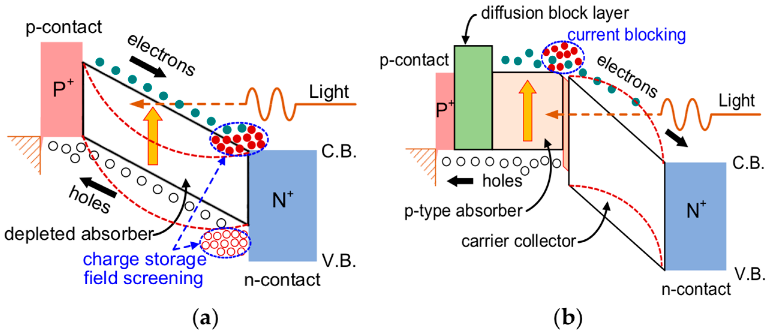
Figure 3.
(a) The cutoff wavelength–related refractive index and permittivity for with the As–composition changed from 0 to 1. (b) Solutions for suppressing the bandgap discontinuity by compositional graded quaternary material and dipole–doping regimes.
Figure 3.
(a) The cutoff wavelength–related refractive index and permittivity for with the As–composition changed from 0 to 1. (b) Solutions for suppressing the bandgap discontinuity by compositional graded quaternary material and dipole–doping regimes.
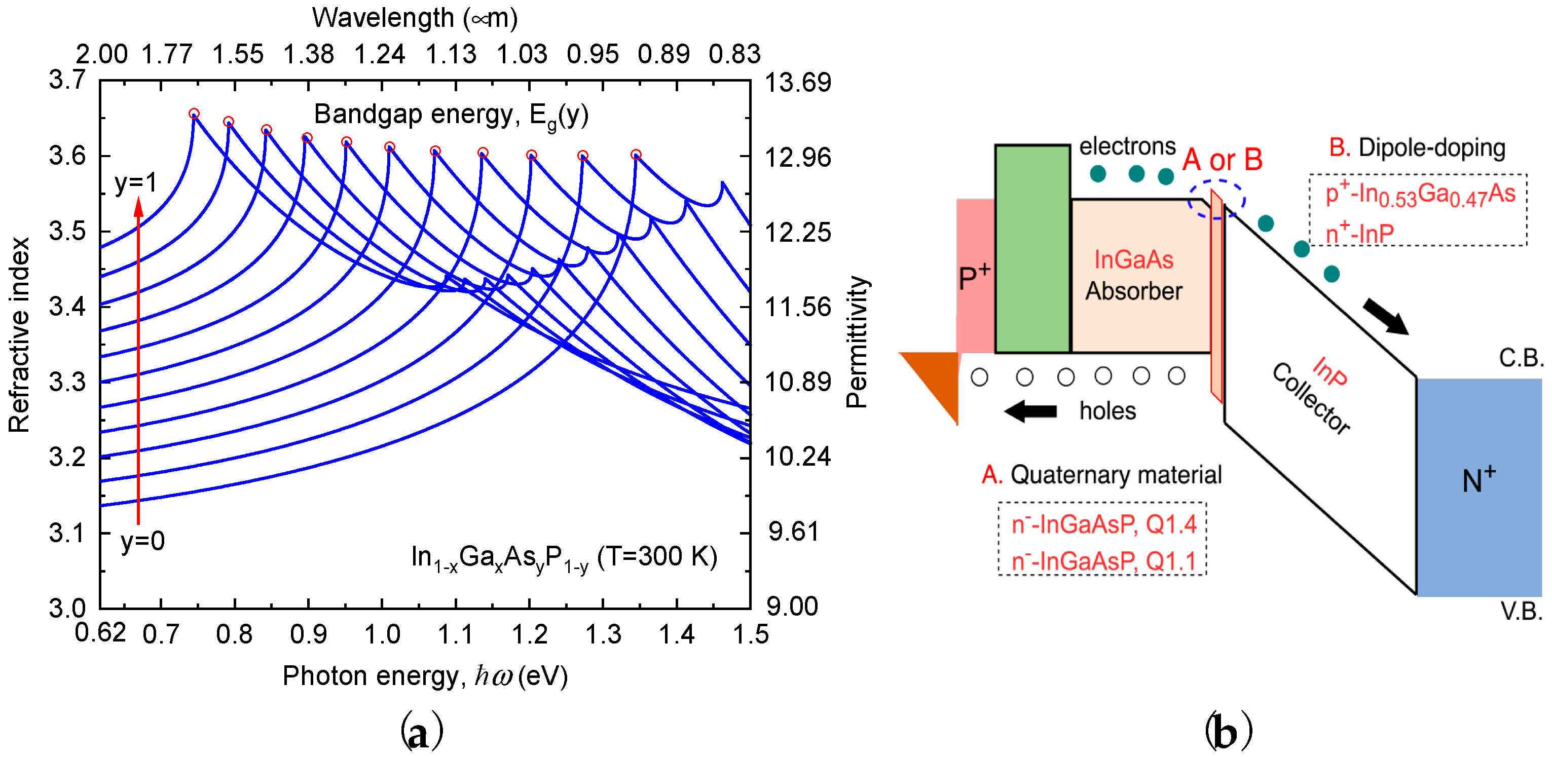
Figure 4.
Cross–sectional diagram of PIN–PD and PD symbol.

Figure 5.
(a)The calculated 3–dB bandwidth versus the absorber thickness for UTC–PD and PIN–PD. (b) The 310 GHz bandwidth [67] is used to indicate the calculated accuracy in (a). (c) Measured and calculated 3–dB bandwidth for UTC–PD (at high and low input) and PIN–PD [44]. (d) Quantum efficiency, responsivity versus 3–dB bandwidth for back–illuminated UTC–PD [44], refracting–facet UTC–PD (RF–PD) [68], and total–reflection UTC–PD (TR–PD) [69].
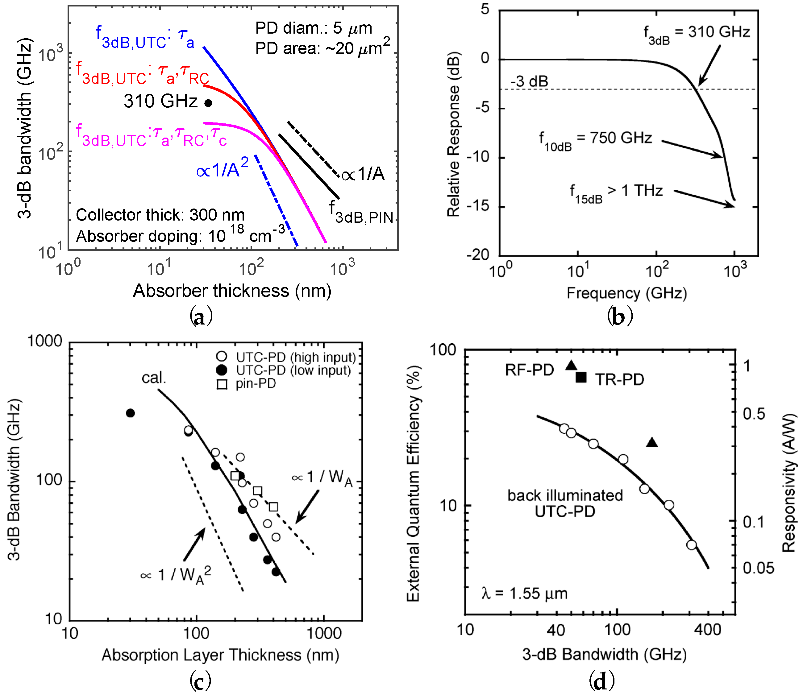
Figure 6.
Band diagrams for designing different kinds of PDs to realize various performances, including high responsivity, high speed, and high power [71,72]. (a) Partially depleted absorber PD (PDA–PD) band diagram [73,74,81]; (b) dual depletion PD band diagram [75,76]; (c) UTC–PD band diagram [31,32,44]; (d) hybrid absorber structure PD band diagram [47,71,72,77]; (e) CC–MUTC–PD band diagram [38,47,78]; and (f) near–ballistic (NB) CC–MUTC–PD band diagram [79,80].
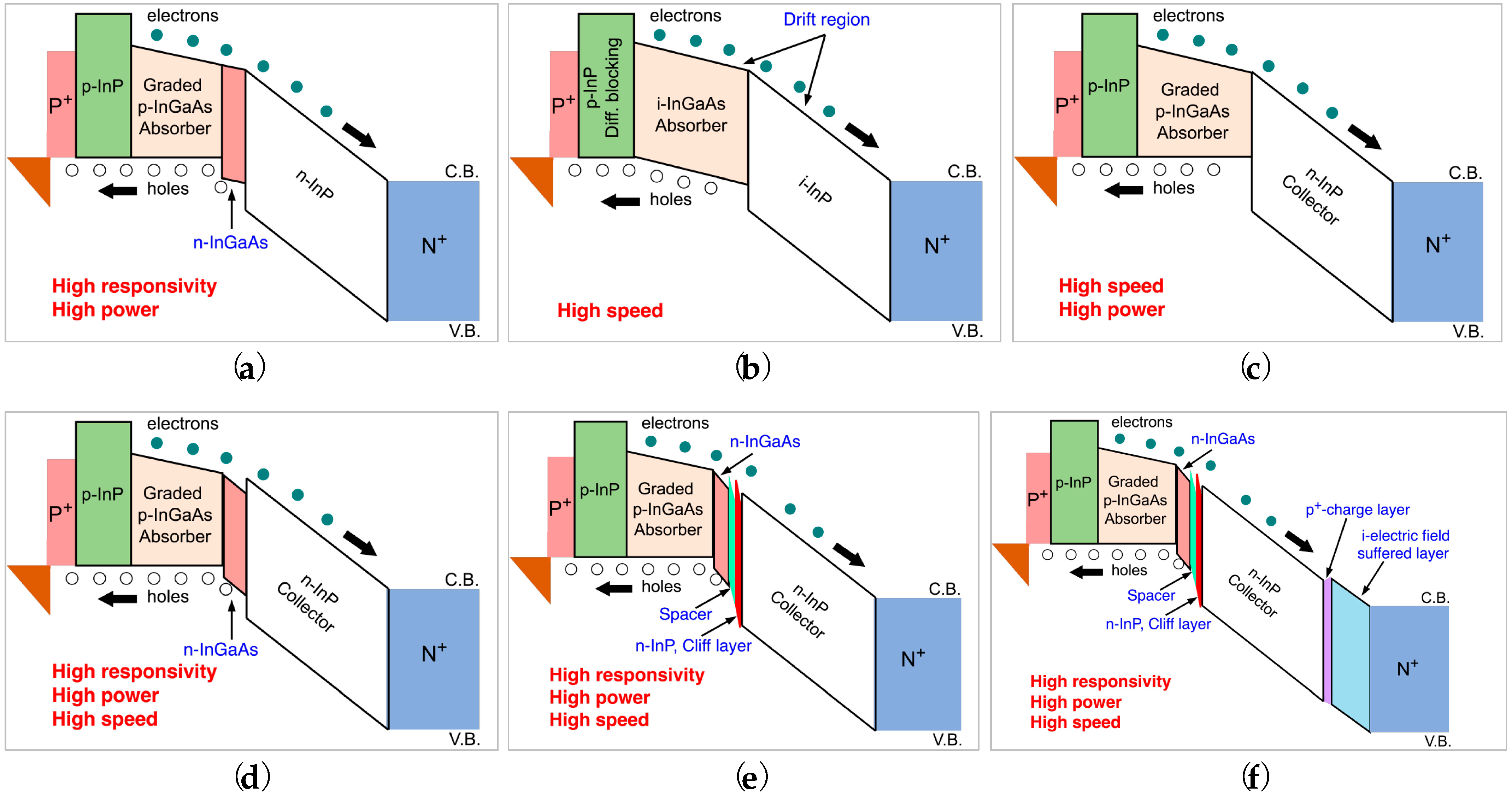
Figure 7.
The calculated electron traveling time in the absorber and collector on 3–dB bandwidth (BW) [44,82,83]. (a) The electron traveling time versus the absorber and collector thickness (assume ); (b) relationship between the 3–dB bandwidth and absorber/collector thickness; (c) comparisons of the calculated electron diffusivity versus p–doping concentration in the absorber [83]; and (d) summary of three p–dopings in the absorber with the calculated values.
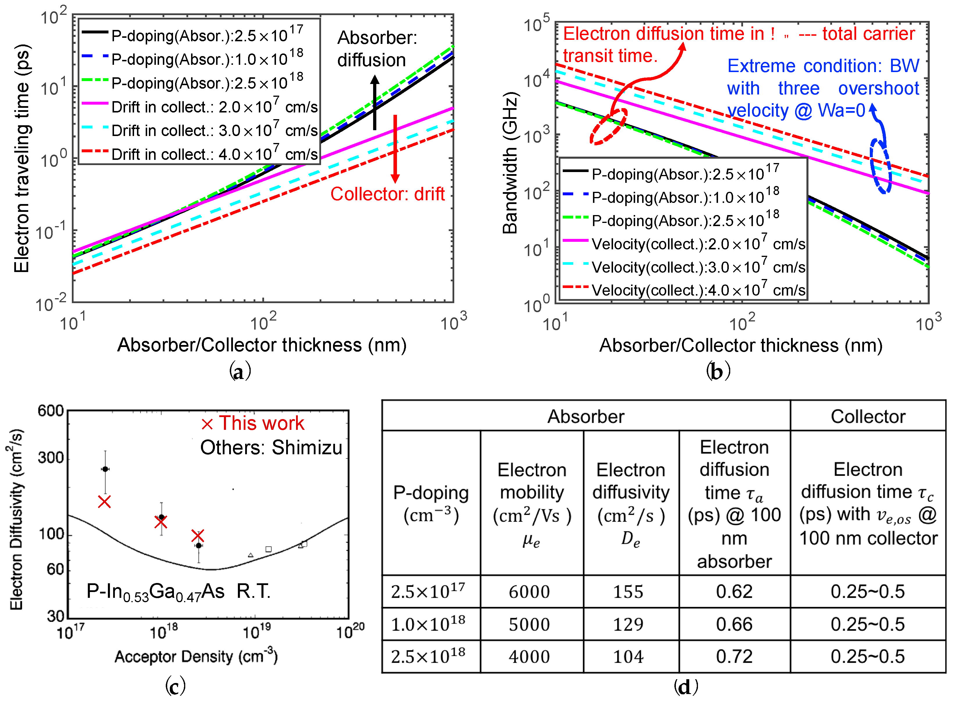

Figure 9.
PD equivalent circuit model with air bridge, coplanar waveguide (CPW) pad, and load resistance.
Figure 9.
PD equivalent circuit model with air bridge, coplanar waveguide (CPW) pad, and load resistance.

Figure 10.
PD equivalent circuit model with coplanar waveguide (CPW) pad and load resistance.
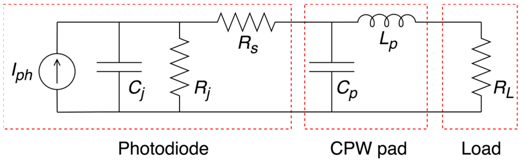
Figure 11.
RF small–signal equivalent circuit model of PD, including internal circuit and external circuits which consist of air bridge, coplanar waveguide (CPW) pad, and load resistance.
Figure 11.
RF small–signal equivalent circuit model of PD, including internal circuit and external circuits which consist of air bridge, coplanar waveguide (CPW) pad, and load resistance.
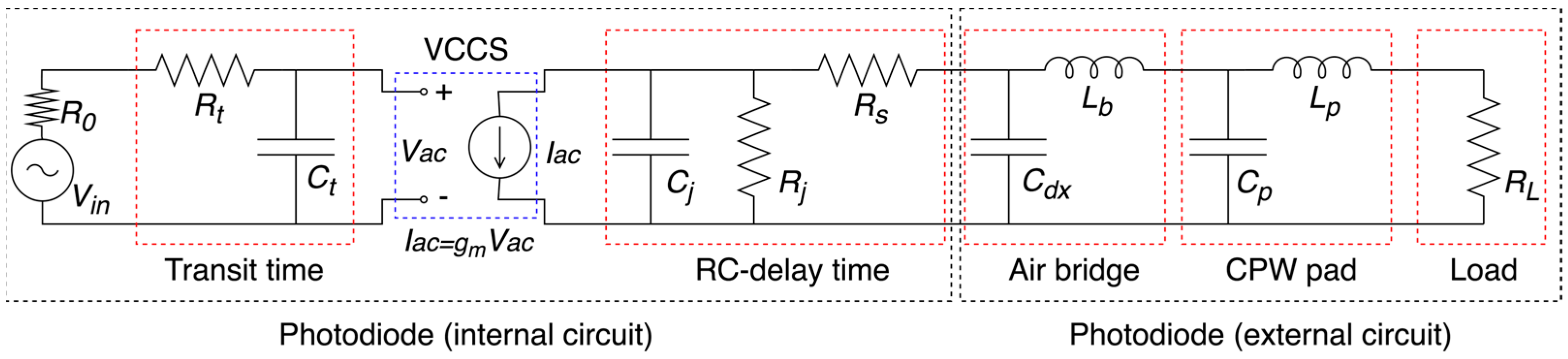

Figure 13.
(a) RF small–signal equivalent circuit model of PD without air–bridge; (b–e) RC–delay time models designed by Li [89], Han [107], Meng [96] and Natrella [99,120].
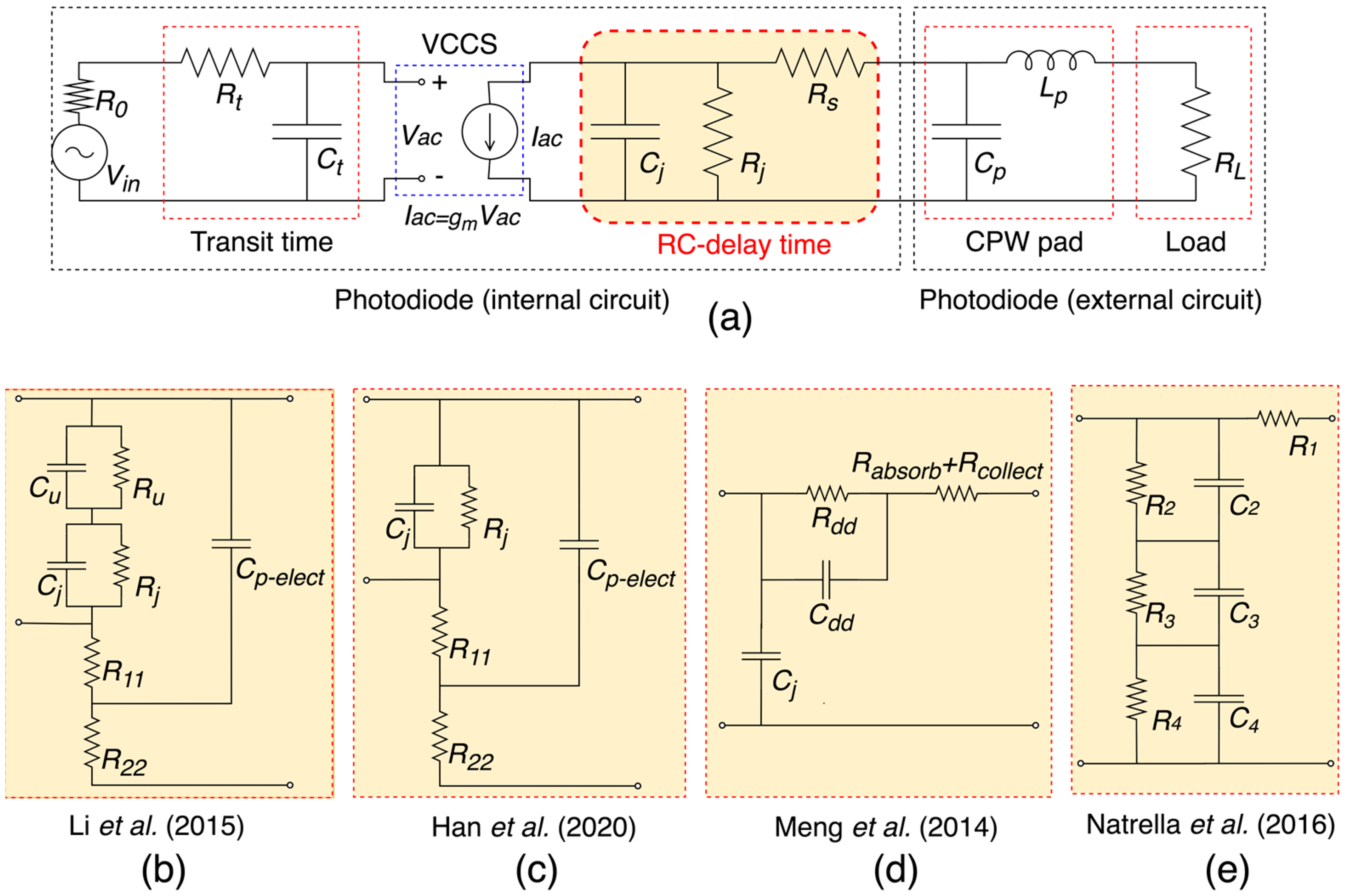
Figure 14.
Equivalent circuit models for MUTC–PD integrated with antennas. (a) Classical equivalent circuit models of MUTC–PD with Vivaldi antenna and matching network [25]; (b) improved equivalent circuit models of CC–MUTC–PD with planer antennas [22].

Figure 15.
Two CPW schematic diagrams, equivalent circuit models, and simulated results [107]. (a) Conventional CPW–1 with 50 Ω impedance and the new CPW–2 with 115 Ω impedance, and the fabricated CPW–1, and CPW2; (b) PD equivalent circuit model (Region 1: transit time; Region 2: RC–delay time; Region 3: CPW pad) and the simulated series inductance and shunt capacitance.

Figure 16.
(a) Flip–chip bonded CC–MUTC–PD; (b) PD junction temperature vs. dissipated power; and (c) junction temperature comparisons for PD with and without submounts [38].
Figure 16.
(a) Flip–chip bonded CC–MUTC–PD; (b) PD junction temperature vs. dissipated power; and (c) junction temperature comparisons for PD with and without submounts [38].
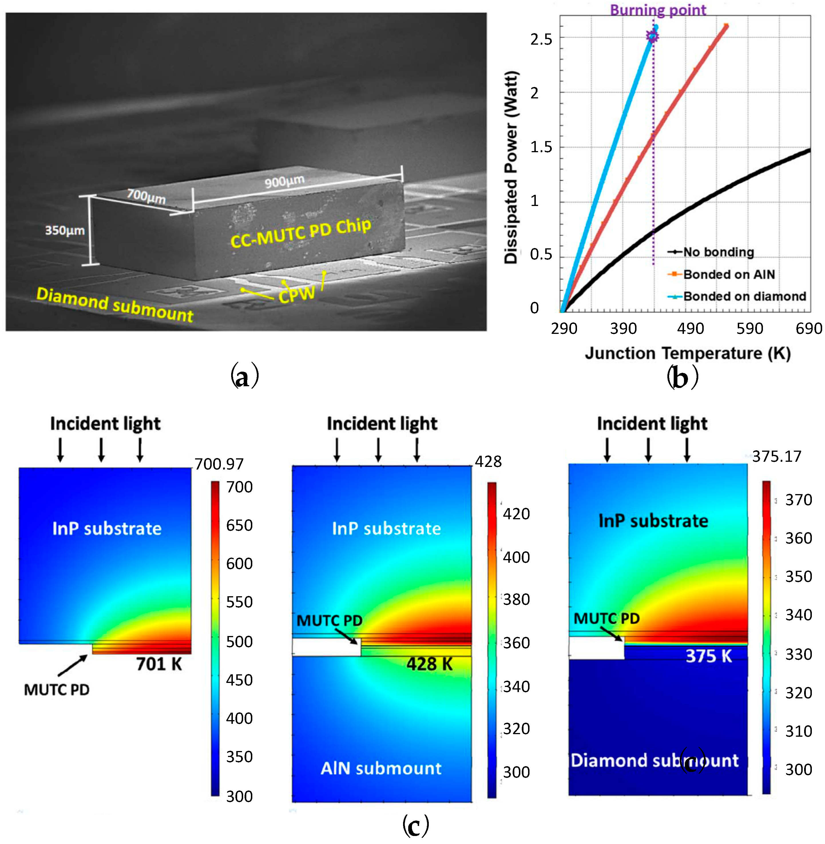
Figure 17.
CC–MUTC–PD RF output power and peak power at different photocurrents and bias voltages. (a) RF power vs. photocurrent with different device diameters and bias voltages [130]; (b) RF power vs. photocurrent with different bias voltages for a 40 μm diameter device [122]; (c) peak power at 10 GHz pulse signal vs. photocurrent with different bias voltages [122]; and (d) peak power at 1 GHz pulse signal vs. photocurrent with different bias voltages [122].
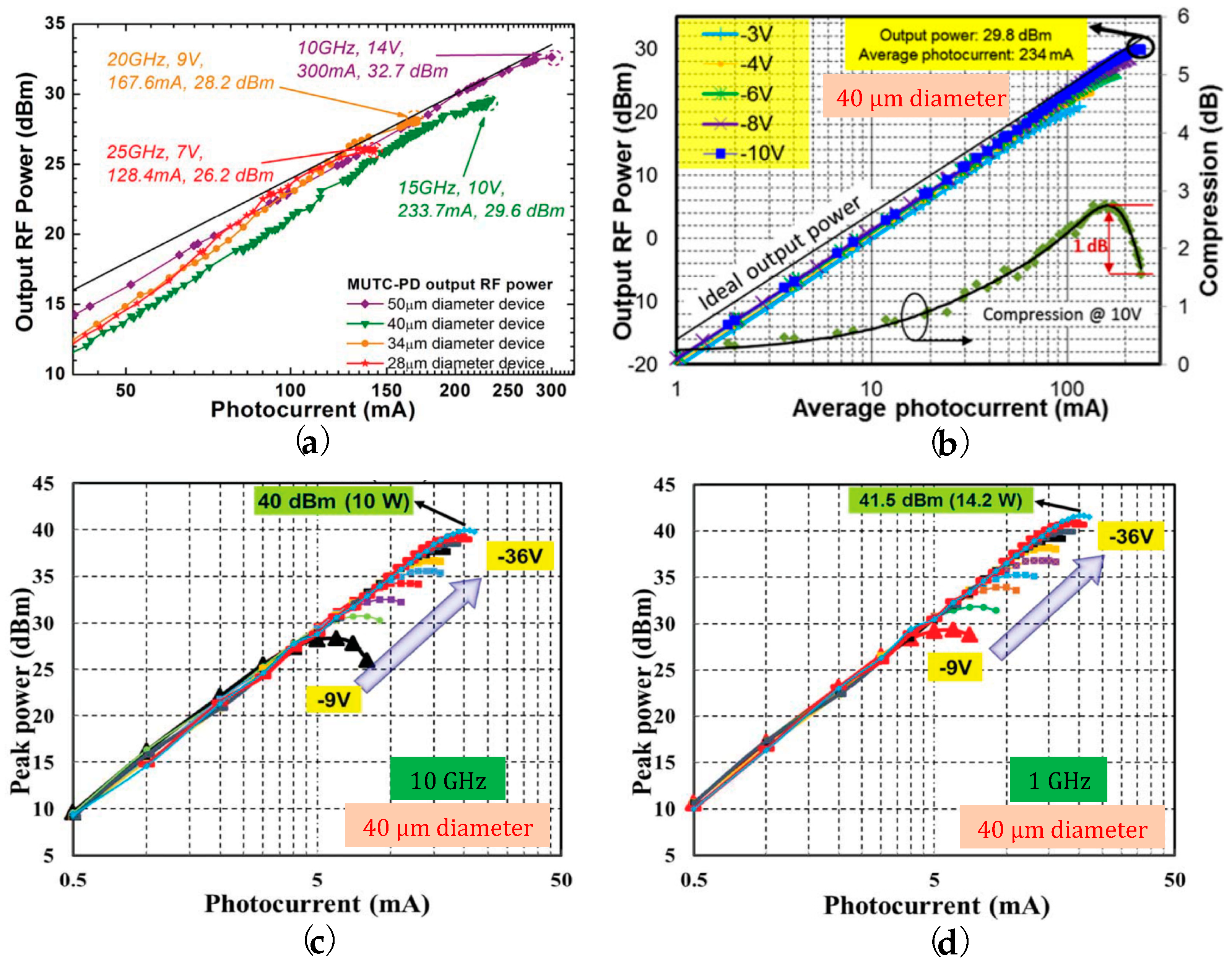
Figure 18.
Two mW RF output power UTC–PD on SiC substrate in 300 GHz band [134]. (a) UTC–PD chip and the packaged module; (b) schematic of UTC–PD and effective–medium (EM) waveguide, while showing the electrical field distribution; (c) UTC–PD chip on SiC, where a short–stub matching circuit and a metal–insulator–metal (MIM) capacitor is used to increase the output power; (d) UTC–PD chip RF output power and photocurrent at 300 GHz; and (e) RF output power and photocurrent at 273 GHz for the packaged module (UTC–PD chip integrated with tapered slot antenna).

Figure 19.
Photodiodes (PIN–PDs or UTC–PDs) are integrated or quasi–integrated with different kinds of bottom mirrors or reflectors. (a) Conventional RCE photodiode model, i.e., photodiode with DBR mirror; (b) photodiode with dual mirrors, i.e., bottom mirrors (DBR or subwavelength grating (SWG) mirrors) and top mirrors (dielectric layers, or SWG or ‘metal’ mirrors); (c) photodiode with SWG–focused mirror; (d) photodiode with tapered holes and bottom mirror (DBR or SWG mirrors); (e) waveguide photodiode with DBR mirror; and (f) waveguide photodiode with SWG–focused mirror (strip SWG or concentric circular SWG mirrors).

Figure 20.
UTC–PDs integrated with different kinds of mirrors. (a) PIN–PD integrated with 4 DBRs forming a four–mirror and three–cavity (M4C3) structure [157]; (b) UTC–PD integrated with high–reflectivity (HR) DBR mirrors, using HR–UTC–PD for short [34]; (c) UTC–PD integrated with non–periodic concentric circular high–contrast grating (NP–CC–HCG, i.e., focusing reflection (FR) mirror), referred to it as FR–UTC–PD [35]; and (d) symmetric–connected UTC–PD array integrated with 2D–SWG beam–splitter [140].
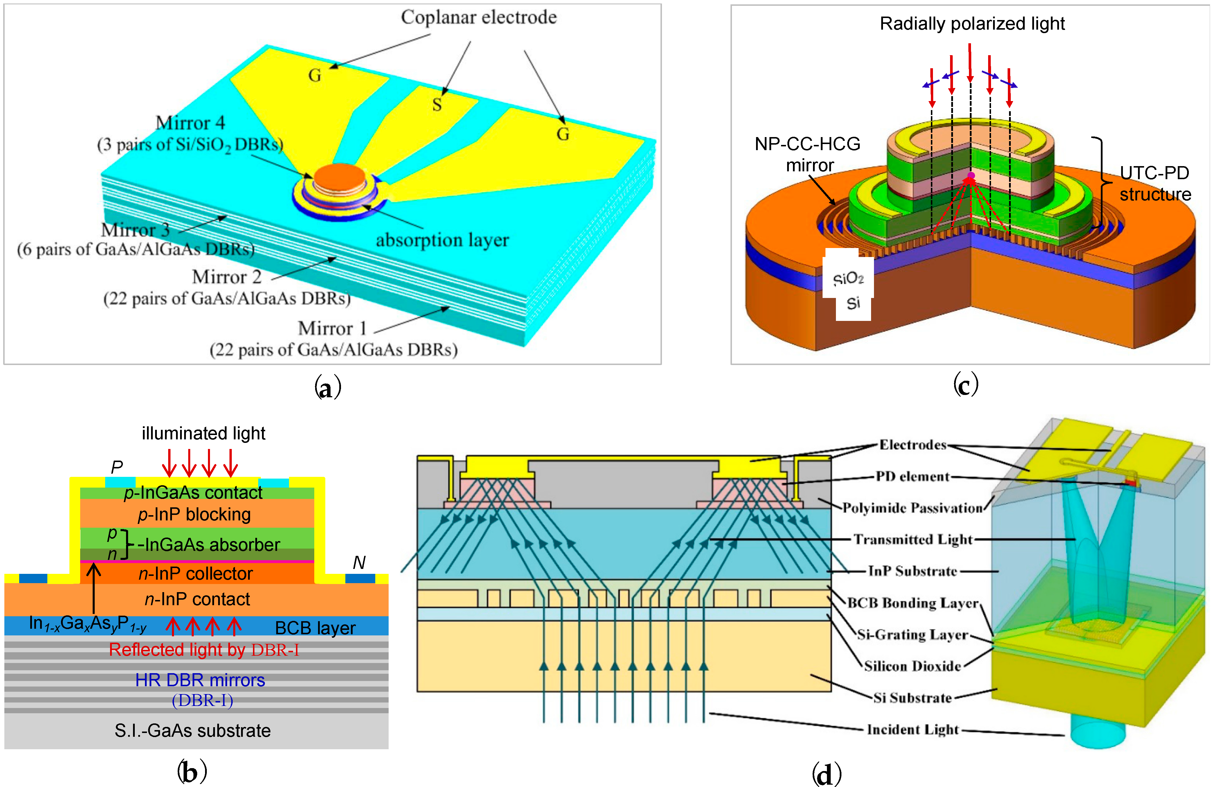
Figure 21.
Photodiodes with different kinds of micro–holes for enhancing light–matter interactions. (a) Schematic of Si–based photodiode with micro–holes [180]: (a1) PD with GSG–pad; (a2) scanning electron micrograph (SEM) of PD active region; (a3) SEM of square holes; (a4) SEM of hexagonal holes. (b) Microstructure PIN photodiode (MPIN–PD) [184]: (b1) schematic diagram; (b2) design of V–groove and center cone.

Figure 22.
Photonic MMW generator (PMG) equivalent circuits and fabricated micrographs [196]. (a,d) PMG–A works at W–band; (b,e) PMG–B works at W–band; (c) relative output power comparisons for PMG–A, PMG–B, and UTC–PD without PMG; and (f) PMG works at J–band [168].
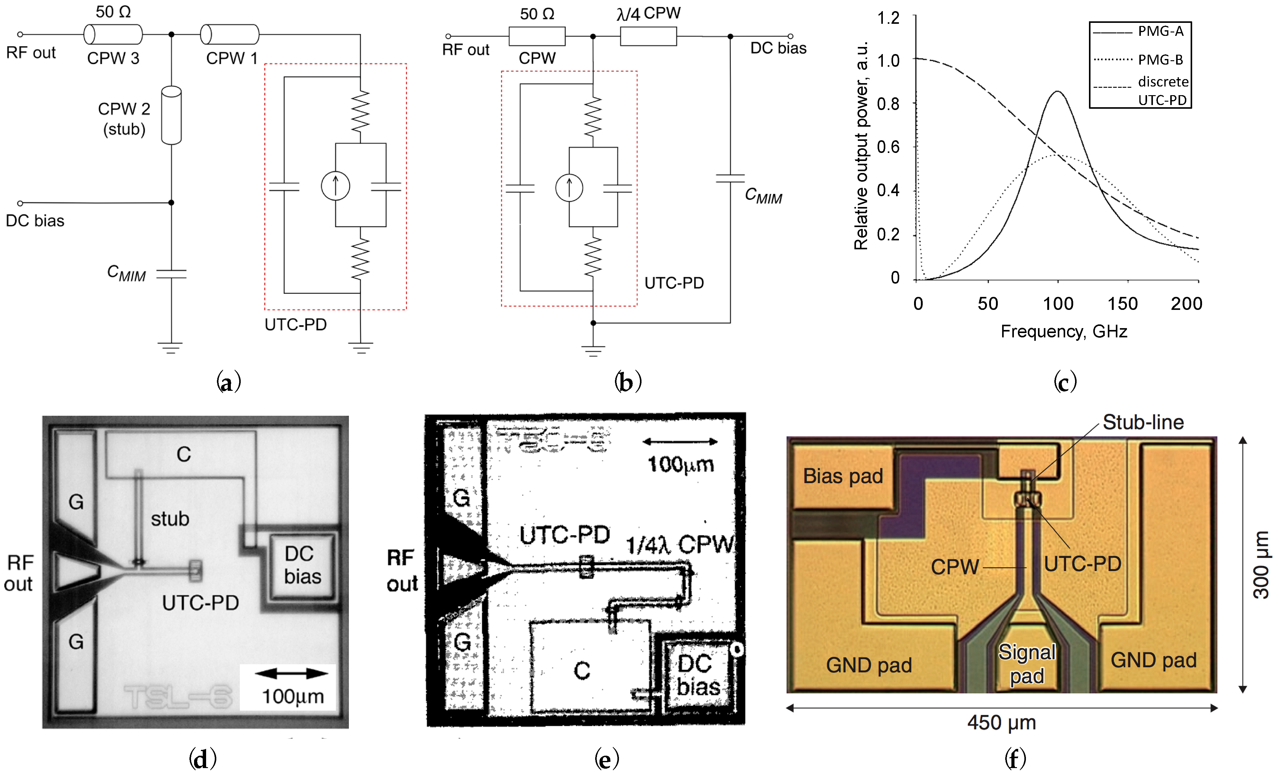
Figure 23.
General schematic diagram of (a) PD photonic–integrated emitter and (b) receiver.
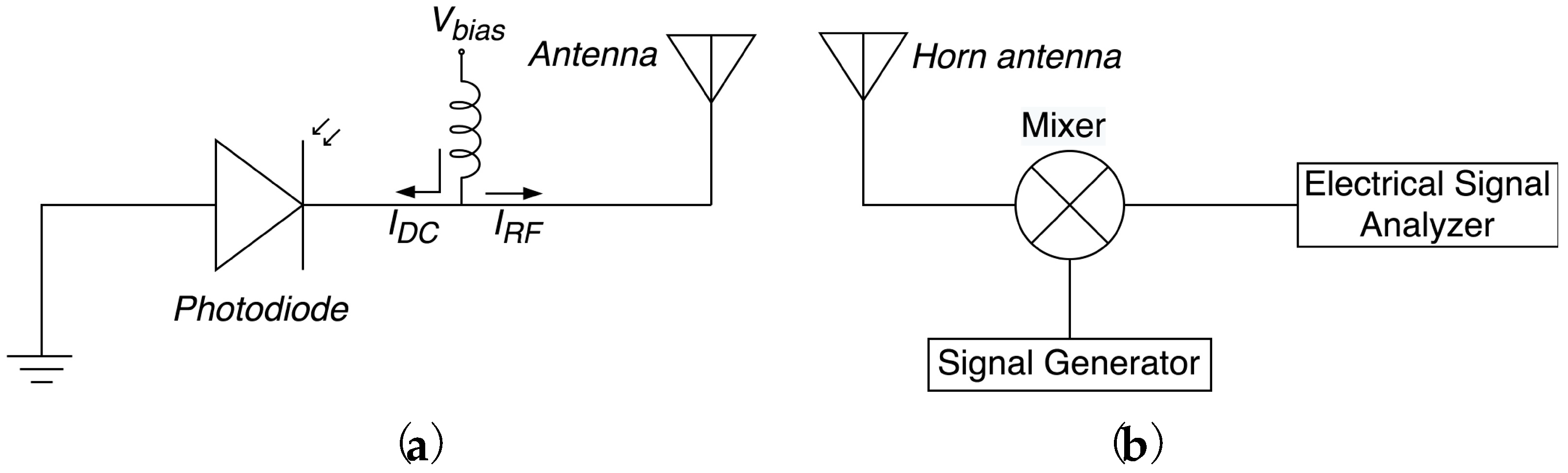
Figure 24.
Schematic diagram of CC–UTC–PD photonic–integrated emitter with Si–lens, the three different planar antennas, and the top/bottom views of the fabricated emitter [22].
Figure 24.
Schematic diagram of CC–UTC–PD photonic–integrated emitter with Si–lens, the three different planar antennas, and the top/bottom views of the fabricated emitter [22].

Figure 25.
(a) UTC–PD integrated with slot antennas used as an MMW signal emitter for free–space applications [123,124]. (b) The fabricated quasi–optical UTC–PD with Si–lens module for practical use [204]. (c,d) UTC–PD integrated with log–periodic antenna (micrograph as shown in the inset) attains 300 μW output power and 20 mA photocurrent at a 1.5 V bias voltage [205].

Figure 26.
InP–based PIN–PD integrated with four bowtie antennas and mounted on Si–lens to increase emitted power and high directivity [206]. (a) The fabricated InP chip and the schematic for packaging of the antenna array; (b) the emitter chip module; and (c) measurement setup.
Figure 26.
InP–based PIN–PD integrated with four bowtie antennas and mounted on Si–lens to increase emitted power and high directivity [206]. (a) The fabricated InP chip and the schematic for packaging of the antenna array; (b) the emitter chip module; and (c) measurement setup.
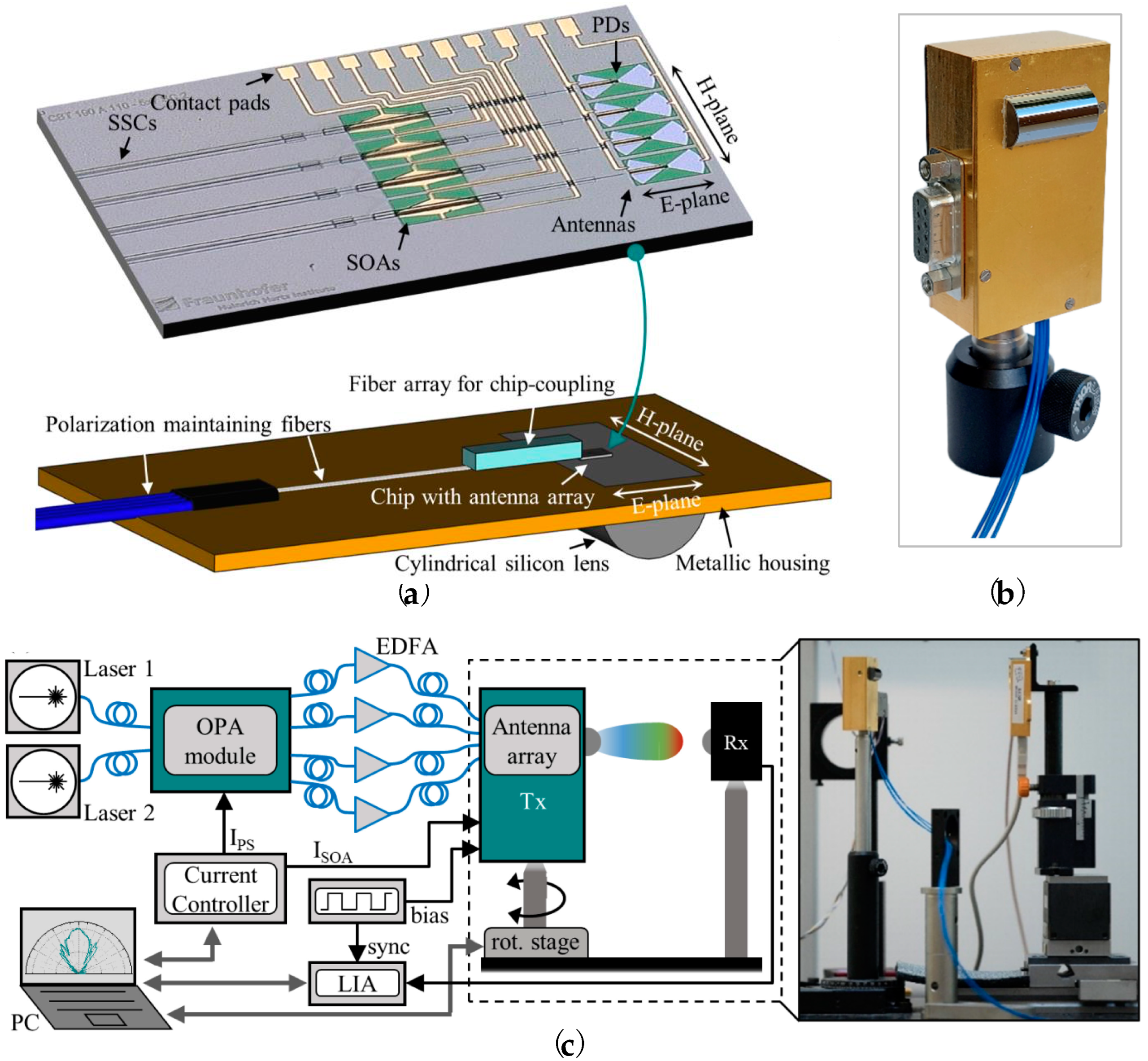
Figure 28.
Traveling–wave UTC–PD (TW–UTC–PD) integrated with resonant, bowtie, and log–periodic antennas, and the radiated power at different photocurrent levels for resonant antenna (a), and for bowtie and log–periodic antennas (b), where the device dimensions are in μm2 [21,222].
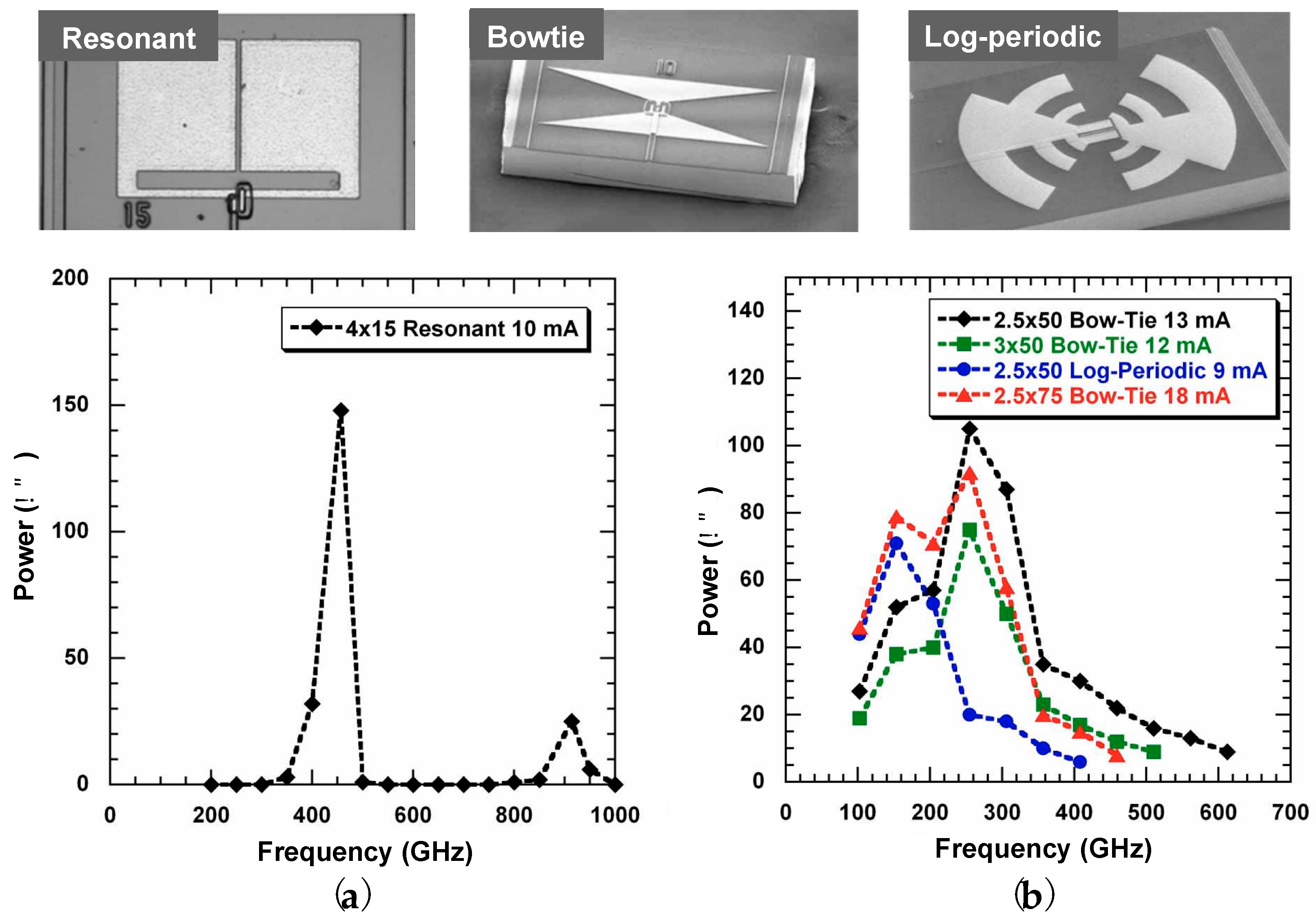
Figure 29.
Hybrid absorber UTC–PD (modified UTC–PD, MUTC–PD) integrated with bowtie antenna [72]. (a) Band diagram of MUTC–PD; (b) MUTC–PD integrated with bowtie antenna; (c) incident light coupling to MUTC–PD by a refracting–facet plane and 45° mirror; (d) frequency response of MUTC–PD with three quasi–field values; (e) comparisons of the measured THz power (open circles) and calculated values of the integrated device using different electron effective velocity, . Note: The inset is the packaged device module (i.e., photomixer) with Si–lens and fiber pigtail.


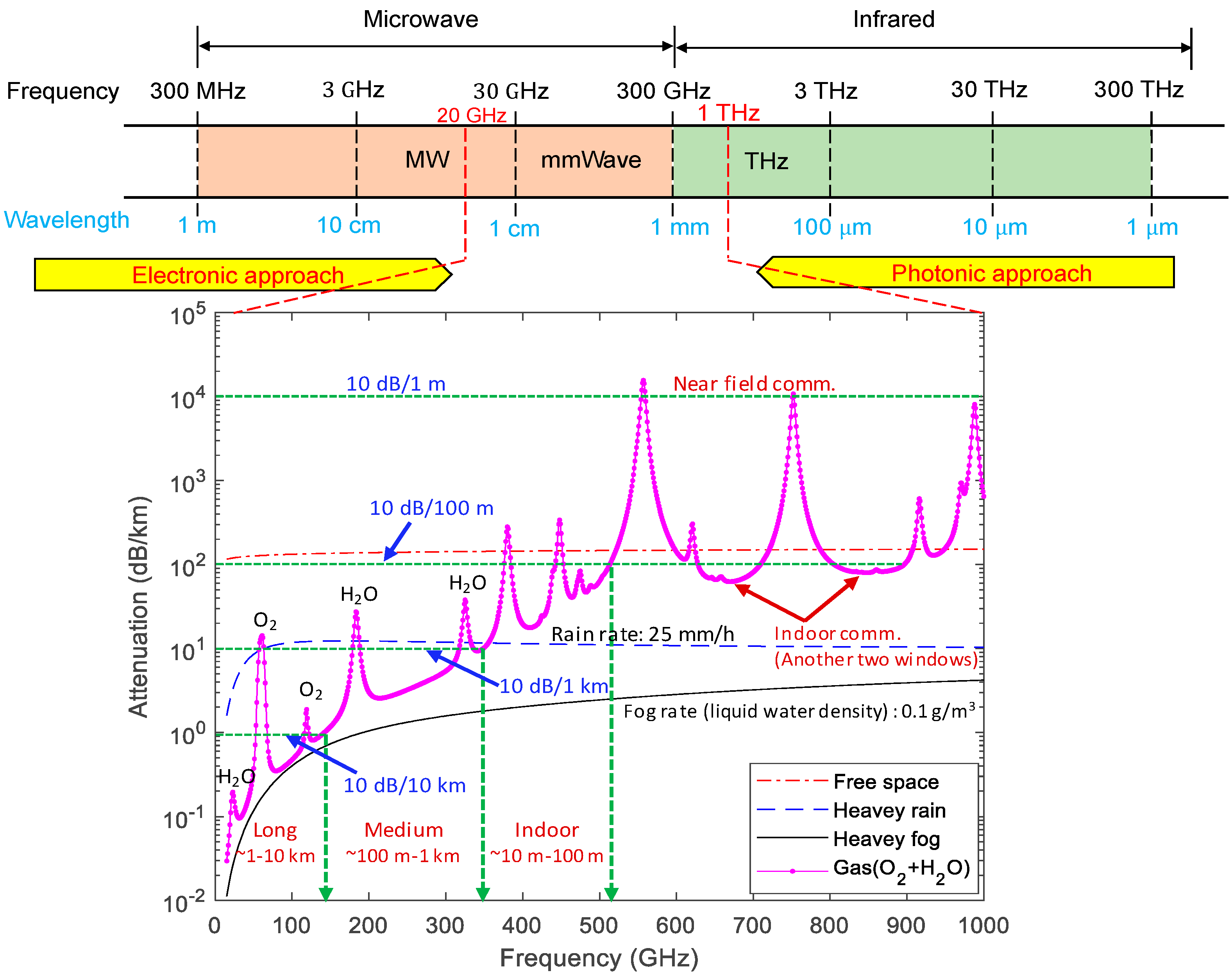
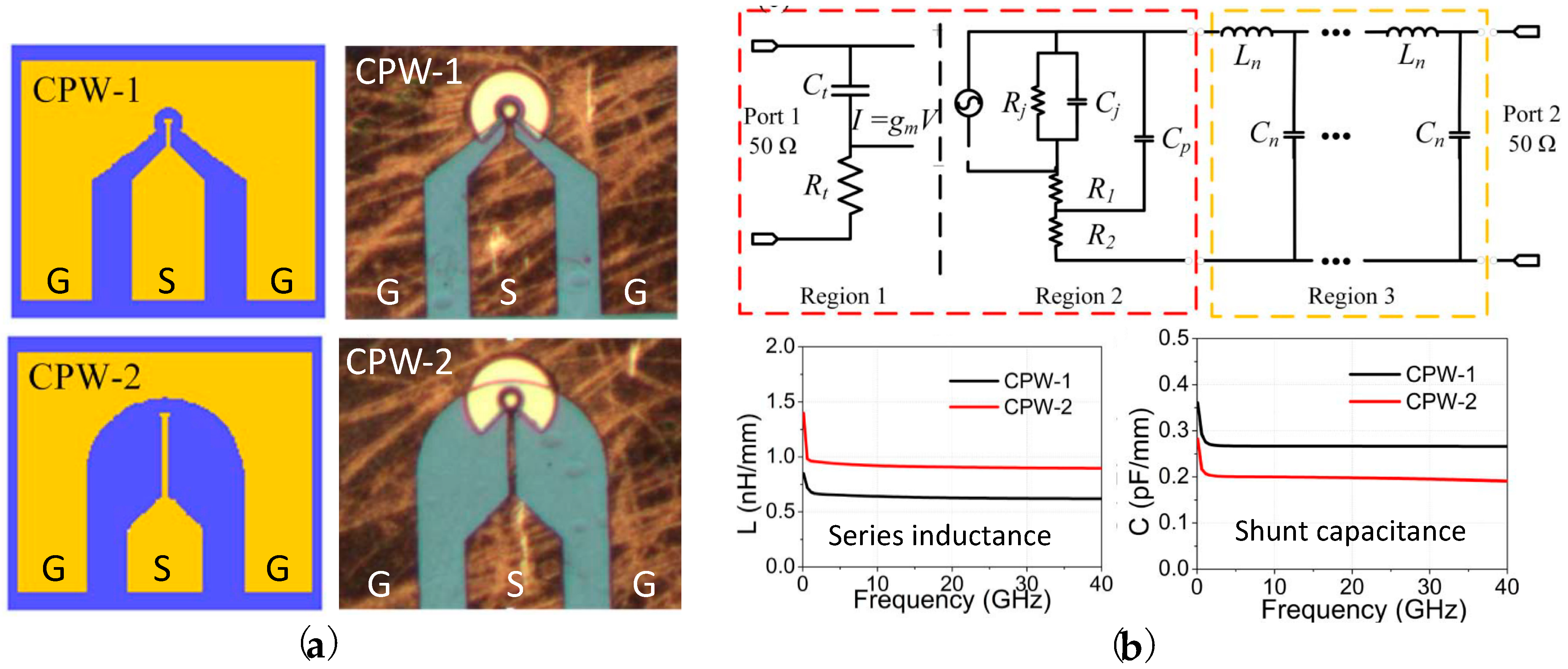
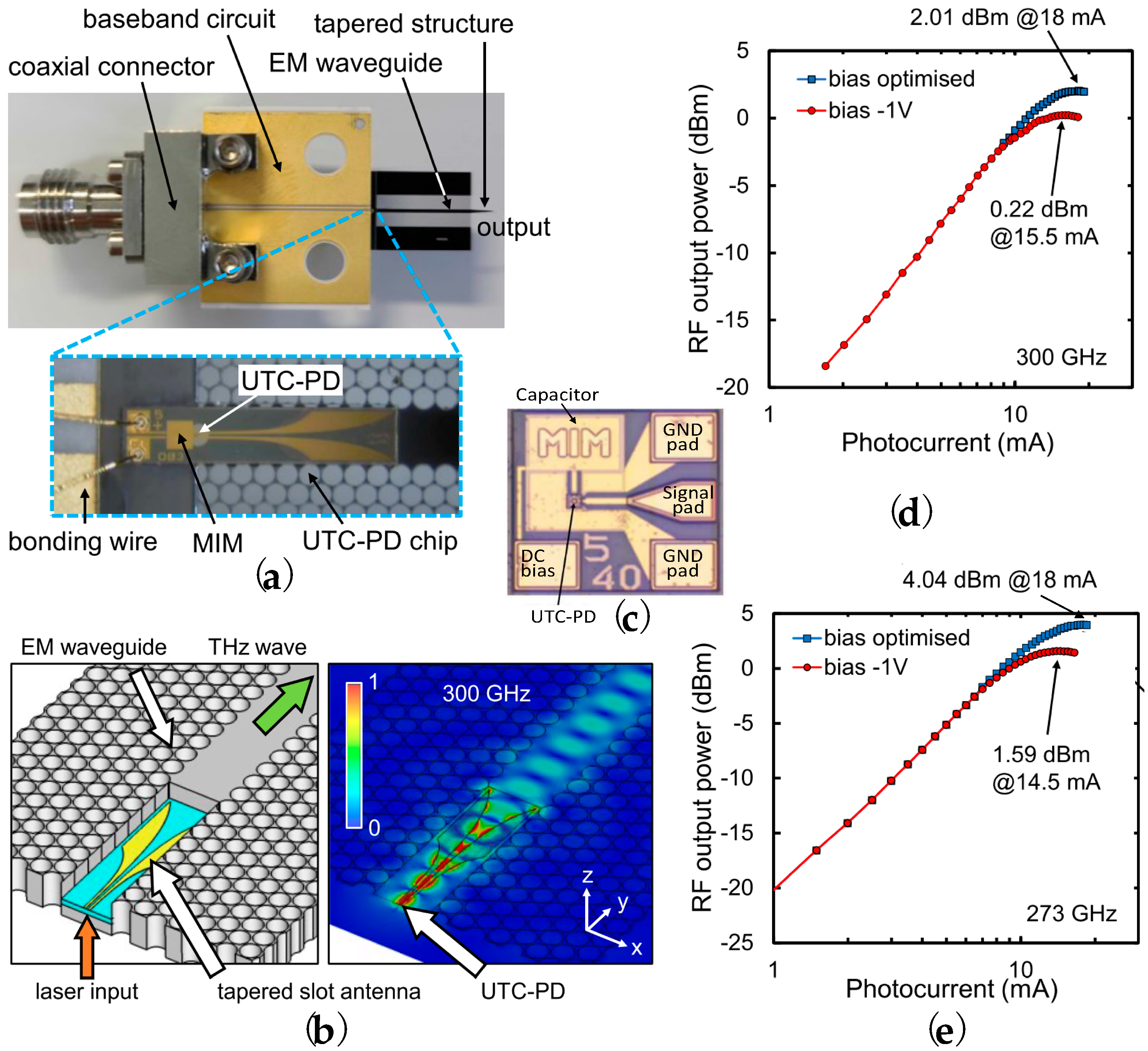
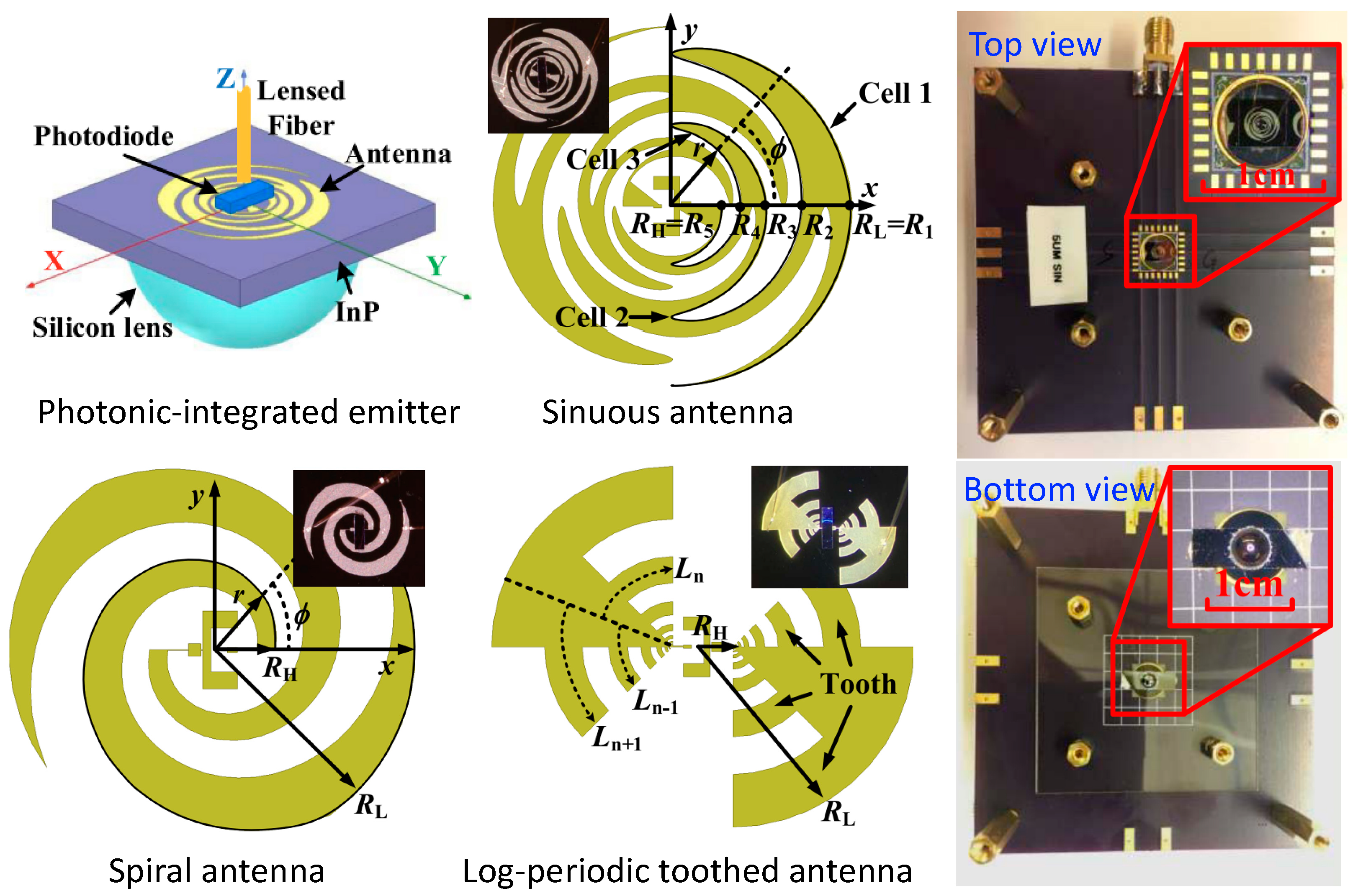
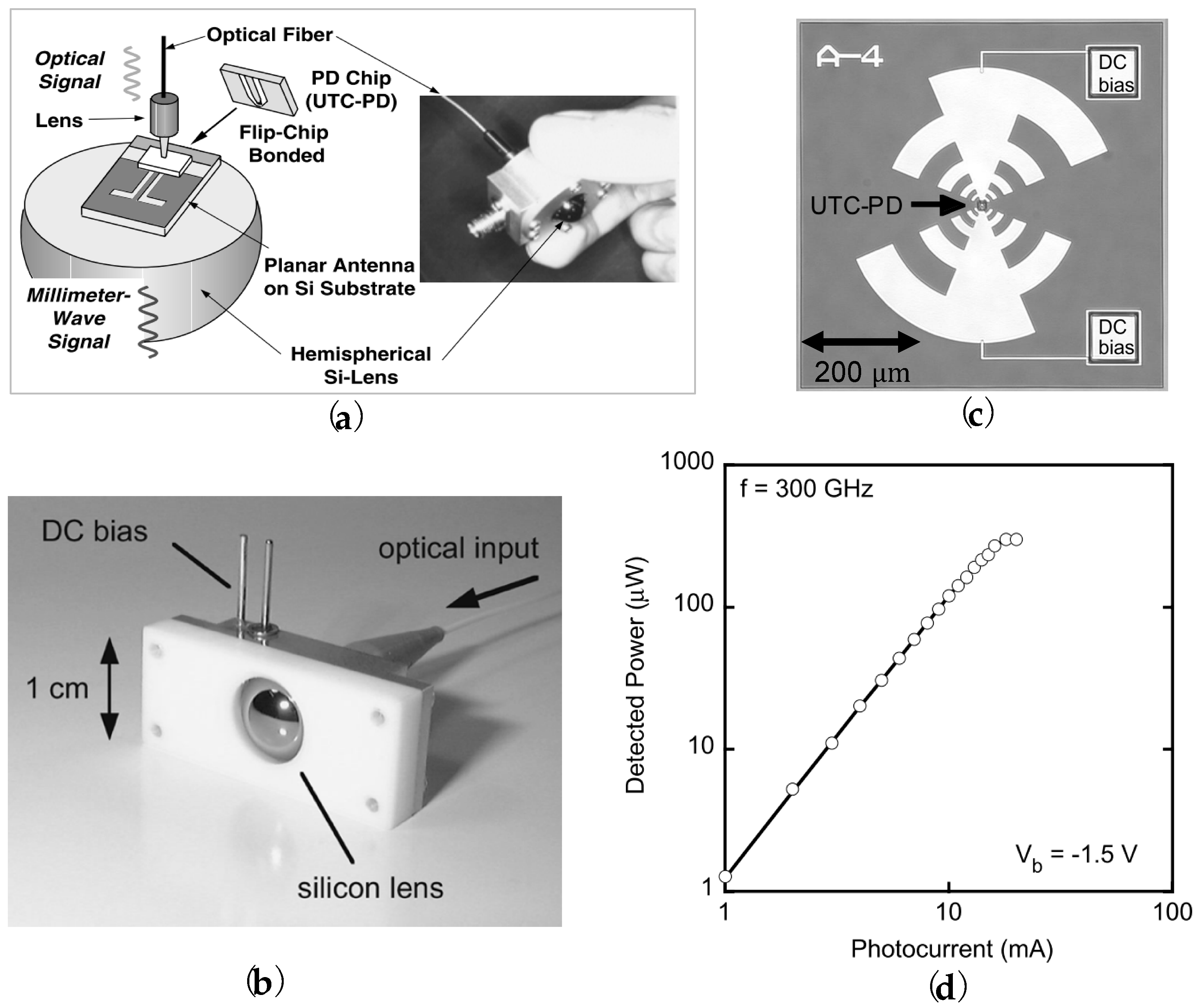
Table 1.
The explanations for parameters [44] used for the 3–dB bandwidth calculation.
Table 1.
The explanations for parameters [44] used for the 3–dB bandwidth calculation.
| Symbol | Value and Units | Explanations |
|---|---|---|
| Boltzmann constant | ||
| Electron charge | ||
| Temperature | ||
| Electron mass in vacuum | ||
| Electron mobility in p–InGaAs | ||
| 150 | Hole mobility in p–InGaAs | |
| Electron overshoot velocity in InGaAs and InP | ||
| Hole saturation velocity | ||
| Electron diffusion constant | ||
| Electron effective mass at the band edge | ||
| Thermionic–emission velocity | ||
| Electron drift velocity in absorber | ||
| Electron diffusion velocity in absorber | ||
| Carrier traveling time by electron diffusion | ||
| Electron drift time in collector | ||
| Boltzmann constant |
Table 2.
The 3–dB bandwidth (BW), saturation current ( or ), responsivity (), bias voltage () and output power () comparisons for PDs.
Table 2.
The 3–dB bandwidth (BW), saturation current ( or ), responsivity (), bias voltage () and output power () comparisons for PDs.
| PD Type * | BW (GHz) ** | R (A/W) | (mA) | Ref. | |
|---|---|---|---|---|---|
| UTC–PD | 310 | 0.07 | NA | 11 (12.59 mW) @ 100 GHz, −0.5 V | [67] |
| NBUTC–PD | 120 (64 μm2, −3.0 V) | 0.15 | 24.6 | 6.28 (4.25 mW) @ 110 GHz, −5 V | [94] |
| NBUTC–PD | 270 (3.5 μm, −3.0 V) | 0.12 | 17 | 6.12 (4.093 mW) @ 170 GHz, −2 V | [95,146] |
| NBUTC–PD | 225 (3 μm, −1.5 V) | 0.08 | 13 | −1.74 (0.67 mW) @ 260 GHz, −2 V | [97] |
| CC–MUTC–PD | >110 (4 μm) | 0.17 | 27 | 7.80 (6.03 mW) @ 110 GHz (6 μm), −4 V | [101] |
| MUTC–PD | 156 (4.5 μm, −3 V) | 0.165 | 14.6 | −0.53 (0.885 mW) @ 170 GHz, −3.5 V | [111] |
| MUTC–PD | 150 (4.5 μm, −3 V) | 0.165 | 14.6 | −0.16 (0.964 mW) @ 170 GHz, −3.5 V | [111] |
| MUTC–PD | 200 (3.6 μm) | 0.07 | 8.4 | −2.14 (0.611 mW) @ 200 GHz, −2 V | [113] |
| MUTC–PD | 230 (3 μm) | 0.07 | 5.85 | −4.94 (0.321 mW) @ 220 GHz, −2 V | [113] |
| CC–MUTC–PD | 105 (10 μm, −5.0 V) | 0.15 | >30 | 14 (25.12 mW) @ 80 GHz (10 μm), −2 V | [114] |
| CC–MUTC–PD | 117 (8 μm, −3.0 V) | 0.15 | >20 | 11.3 (13.49 mW) @ 100 GHz (8 μm), −2 V | [114] |
| CC–MUTC–PD | 117 (8 μm, −3.0 V) | 0.15 | >20 | 8.50 (7.08 mW) @ 110 GHz (8 μm), −2.5 V | [114] |
| CC–MUTC–PD | 150 (4 μm, −3.0 V) | 0.15 | 8.0 | ), −2.5 V | [114] |
| CC–MUTC–PD | , −1.1 V) | 0.11 | 4.9 | ), 0 V | [115] |
| CC–MUTC–PD | , −1.1 V) | 0.11 | 25.3 | ), −1.8 V | [115] |
| WG–MUTC–PD | −1.2 V) | 0.312 | 10.6 | –1.69 (0.678 mW) @ 215 GHz, −2 V | [119] |
| CC–MUTC–PD | ) | 0.2 | 40 | –2.60 (0.55 mW) @ 160 GHz, −5 V | [121] |
| CC–MUTC–PD | , −6 V) | 0.7 | 234 (−10 V) | 41.5 (14.2 W) @ 1 GHz, −36 V | [122] |
| CC–MUTC–PD | , −6 V) | 0.7 | 234 (−10 V) | 40 (10 W) @ 10 GHz, −36 V | [122] |
| CC–MUTC–PD | , −6 V) | 0.7 | 234 (−10 V) | 29.8 (0.955 W) @ 15 GHz, −10 V | [122] |
| UTC–PD | ) | NA | 21 | 0 (1 mW) @ 120 GHz, −3V | [123,124] |
| CC–MUTC–PD | ) | 0.75 | 300 | 32.7 (1.86 W) @ 10 GHz, −14 V | [130] |
| CC–MUTC–PD | ) | 0.75 | 228 | 30.1 (1.02 W) @ 10 GHz, −11 V | [131] |
| UTC–PD on SiC | NA | NA | 15.5 | 0.22 (1.05 mW) 300 GHz, −1 V | [134] |
| UTC–PD on SiC | NA | NA | 18 | 2.01 (1.59 mW) 300 GHz, bias optimized | [134] |
| PIN–PD | ) | NA | 620 | 26.5 (0.447 W) @ 1 GHz, −5 V | [136] |
| PIN–PD | ) | NA | 260 | 26 (0.398 W) @ 6 GHz, −5 V | [136] |
| PIN–PD | ) | 0.55 | 120 | 25.8 (0.38 W) @ 5 GHz | [137] |
| PIN–PD | ) | 0.6 | 200 | 29 (0.794 W) @ 5 GHz, −5.8 V | [138] |
| PIN–PD | ) | ~0.7 | 30 | 14 (25.12 mW) @ 50 GHz, −2 V | [139] |
| MUTC–PD array | ) | 0.438 | 86.8 | 16 (39.81 mW) @ 12 GHz, −3 V | [140] |
| MUTC–PD | −4 V) | 0.41 | ~70 | 17.1 (51.29 mW) @ 30 GHz, −4 V | [141] |
| MUTC–PD | −4 V) | 0.41 | 38 | 14.6 (28.84 mW) @ 40 GHz, −4 V | [141] |
| WG–UTC–PD | −3 V) | 0.19 | 13 | 1.1 (1.29 mW) @ 100 GHz, −3 V | [142] |
| TTR–UTC–PD | ) | 0.5 | 16 | 0 (1 mW) @ 110 GHz, −8 V | [143] |
| NBUTC–PD | , −3.0 V) | 0.15 | 13.6 | 1.85 (1.53 mW) @ 110 GHz, −3 V | [144] |
| NBUTC–PD | , −3.0 V) | 0.15 | 18 | 4.12 (2.58 mW) @ 110 GHz, −3 V | [144] |
| NBUTC–PD | , −3.0 V) | 0.15 | 29 | 8.10 (6.46 mW) @ 110 GHz, −3 V | [144] |
| NBUTC–PD | , −3.0 V) | 0.15 | 37 | 10.7 (11.75 mW) @ 110 GHz, −3 V | [144] |
| Type–II UTC–PD | , 0 V) | 0.09 | 8 | ) @ 160 GHz, 0 V | [145] |
| NBUTC–PD | , −0.5 V) | 0.1 | 13 | 0.174 (1.04 mW) @ 280 GHz, −1.2 V | [147,148] |
| RCE–UTC–PD | ) | 0.12 | 9.8 | –1.25 (0.75 mW) @ 300 GHz, −1 V | [149] |
| Two UTC–PD | 70 per PD | 0.17 | 20 | 0.79 (1.2 mW) @ 300 GHz, −3.9 V | [150] |
| Type–II UTC–PD | , −0.5 V) | 0.11 | 13 | –3 (0.5 mW) @ 320 GHz, −1 V | [151] |
| MUTC–PD | ~100 | 0.22 | 20 | –2.7 (0.54 mW) @ 350 GHz, −2.5 V | [152] |
* Waveguide–type PDs are denoted as ‘WG’, while others are vertical double–mesa PDs. ** PD diameter, area, and bias voltage are shown in brackets.
Table 3.
The comparisons of PDs integrated with WR ports and short stubs.
| Device Type | Coupling Type | Si Lens | (mA) | Output Power (dBm) | Ref. |
|---|---|---|---|---|---|
| UTC–PD | WR10 port (W–band) | No | 25 | ) @ 100 GHz | [90] |
| UTC–PD | WR3 port (J–band) | No | 26 | ) @ 264 GHz | [190] |
| UTC–PD | WR8 port (F–band) | No | 25 | ) @ 120 GHz | [197,198] |
| UTC–PD | WR6 port (D–band) | No | 7 | ) @ 104~185 GHz | [200] |
| Coupler integrated UTC–PD | WR1.5 port | No | 9 | ) @ 500 GHz | [201] |
| Coupler integrated UTC–PD | WR1.5 port | No | 9 | ) @ 470~810 GHz | [201] |
| Coupler integrated UTC–PD | WR1.5 port | No | 6 | ) @ 500 GHz | [201] |
| Coupler integrated UTC–PD | WR1.5 port | No | 6 | ) @ 470~810 GHz | [201] |
Table 4.
The comparisons of emitted power for PDs integrated with antennas.
| Device Type * | Coupling Type | Si Lens | (mA) | Output Power (dBm) | Ref. |
|---|---|---|---|---|---|
| NBUTC–PD | Yagi antenna | No | 30 | –14.1 (25.7 mW) @ 100 GHz | [18,223] |
| TW–UTC–PD | Log–periodic antenna | No | 9 | ) @ 150 GHz | [21] |
| TW–UTC–PD | Bowtie antenna | No | 13 | ) @ 255 GHz | [21] |
| TW–UTC–PD | Resonant antenna | No | 10 | ) @ 457 GHz | [21] |
| TW–UTC–PD | Bowtie antenna | No | 13 | ) @ 612 GHz | [21] |
| TW–UTC–PD | Resonant antenna | No | 10 | ) @ 914 GHz | [21] |
| CC–MUTC–PD | Log–periodic antenna | Yes | 7 | 9.9 (9.77 mW) @ 70 GHz | [22] |
| CC–MUTC–PD | Sinuous antenna | Yes | 7 | 11.5 (14.13 mW) @ 90 GHz | [22] |
| CC–MUTC–PD | Sinuous antenna | Yes | 20 | 20 (100 mW) @ 90 GHz | [22] |
| CC–MUTC–PD | Spiral antenna | Yes | 7 | 8.8 (7.59 mW) @ 100 GHz | [22] |
| MUTC–PD | Vivaldi antennas | No | 10 | 5 (3.2 mW) @ 110 GHz | [25] |
| Hybrid absorber UTC–PD | Bowtie antenna | Yes | 6 | ) @ 300 GHz | [72] |
| Hybrid absorber UTC–PD | Bowtie antenna | Yes | 6 | ) @ 1 THz | [72] |
| Hybrid absorber UTC–PD | Bowtie antenna | Yes | 6 | ) @ 1.5 THz | [72] |
| Hybrid absorber UTC–PD | Bowtie antenna | Yes | 6 | ) @ 2 THz | [72] |
| Hybrid absorber UTC–PD | Bowtie antenna | Yes | 6 | ) @ 2.5 THz | [72] |
| MUTC–PD | Patch antenna | No | 45 | 20 (100 mW) @ 60 GHz | [98] |
| TWPD | Bowtie antenna | Yes | 6.3 | ) @ 40 GHz | [91] |
| UTC–PD | Slot antenna | Yes | >20 | –5.23 (0.3 mW) @ 120 GHz | [123,124] |
| UTC–PD on SiC | Tapered slot antenna | No | 14.5 | 1.59 (1.44 mW) @ 273 GHz, −1 V | [134] |
| UTC–PD on SiC | Tapered slot antenna | No | 18 | 4.04 (2.53 mW) @ 273 GHz, bias optimized | [134] |
| WG–UTC–PD | Bowtie antenna | Yes | 13.5 | −12.22 (60 μW) @ 250 GHz | [142] |
| UTC–PD | Log–periodic antenna | Yes | 13 | −25.9 (2.6 μW) @ 1.04 THz | [204] |
| UTC–PD | Log–periodic antenna | Yes | 20 | −5.23 (300 μW) @ 300 GHz | [205] |
| PIN–PD array | Bowtie antenna | Yes | NA | >10 dB vs. an emitter @ 300 GHz | [206] |
| UTC–PD | Log–periodic antenna | Yes | 15 | −11.2 (75 μW) @ 414 GHz | [208] |
| UTC–PD | Log–periodic antenna | Yes | 15 | −17.4 (18 μW) @ 609 GHz | [208] |
| UTC–PD | Log–periodic antenna | Yes | 15 | −20.8 (8.3 μW) @ 804 GHz | [208] |
| UTC–PD | Twin dipole antenna | Yes | 14 | −19.6 (10.9 μW) @ 1.04 THz | [209] |
| UTC–PD | Log–periodic antenna | Yes | 20 | −9.2 (120 μW) @ 300 GHz | [224] |
| Type–II UTC–PD | Dual–ridge horn antenna | No | NA | −15 (31.6 μW) @ 240 GHz | [225] |
| UTC–PD | TEM–horn antenna | Yes | 2.75 | −29.5 (1.13 μW) @ 940 GHz | [226] |
| UTC–PD | TEM–horn antenna | Yes | 2.5 | −33.4 (0.46 μW) @ 1.04 THz | [226] |
| UTC–PD | TEM–horn antenna | Yes | 2.88 | −35.1 (0.31 μW) @ 1.365 THz | [226] |
| UTC–PD | slot antenna | Yes | 10 | −15.53 (28 μW) @ 700 GHz | [227] |
| UTC–PD | slot antenna | Yes | 10 | −24.56 (3.5 μW) @ 1.25 THz | [227] |
* Waveguide– and traveling–wave–type PDs are denoted as ‘WGPD’ and TWPD, while others are vertical–mesa PDs.
Disclaimer/Publisher’s Note: The statements, opinions and data contained in all publications are solely those of the individual author(s) and contributor(s) and not of MDPI and/or the editor(s). MDPI and/or the editor(s) disclaim responsibility for any injury to people or property resulting from any ideas, methods, instructions or products referred to in the content. |
© 2024 by the authors. Licensee MDPI, Basel, Switzerland. This article is an open access article distributed under the terms and conditions of the Creative Commons Attribution (CC BY) license (https://creativecommons.org/licenses/by/4.0/).
Share and Cite
MDPI and ACS Style
Chen, Q.; Zhang, X.; Sharawi, M.S.; Kashyap, R. Advances in High–Speed, High–Power Photodiodes: From Fundamentals to Applications. Appl. Sci. 2024, 14, 3410. https://doi.org/10.3390/app14083410
AMA Style
Chen Q, Zhang X, Sharawi MS, Kashyap R. Advances in High–Speed, High–Power Photodiodes: From Fundamentals to Applications. Applied Sciences. 2024; 14(8):3410. https://doi.org/10.3390/app14083410
Chicago/Turabian StyleChen, Qingtao, Xiupu Zhang, Mohammad S. Sharawi, and Raman Kashyap. 2024. "Advances in High–Speed, High–Power Photodiodes: From Fundamentals to Applications" Applied Sciences 14, no. 8: 3410. https://doi.org/10.3390/app14083410
Note that from the first issue of 2016, this journal uses article numbers instead of page numbers. See further details here.