
2D Saturable Absorbers for Fibre Lasers


Abstract
:
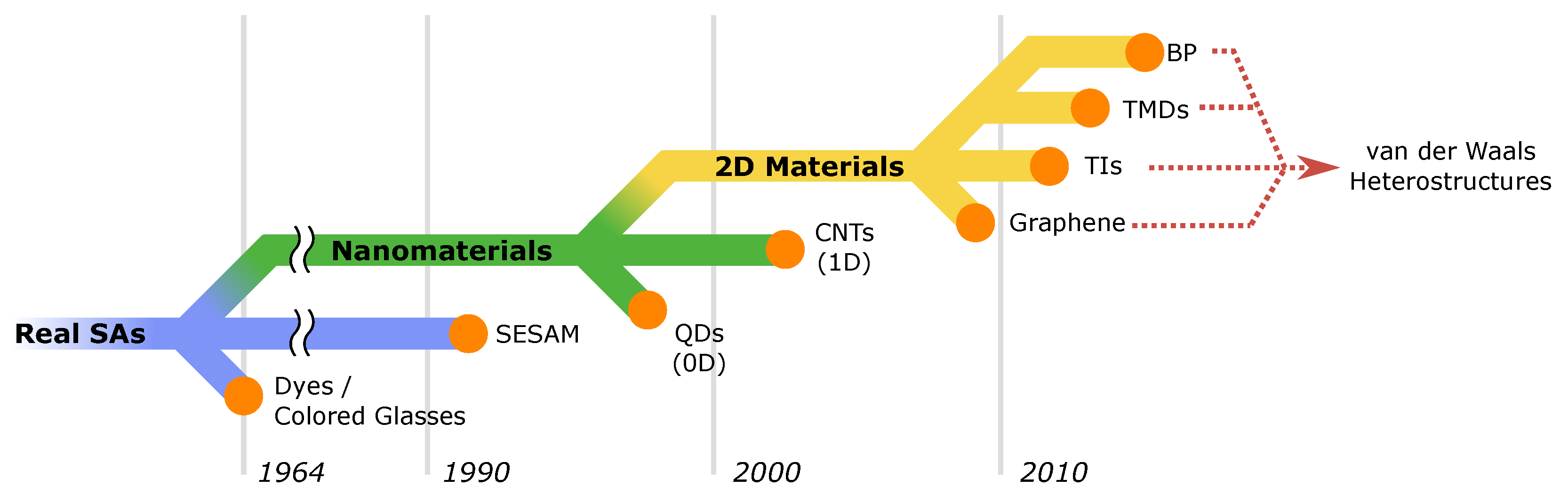
1. Introduction

2. Few-Layer Transition Metal Dichalcogenides
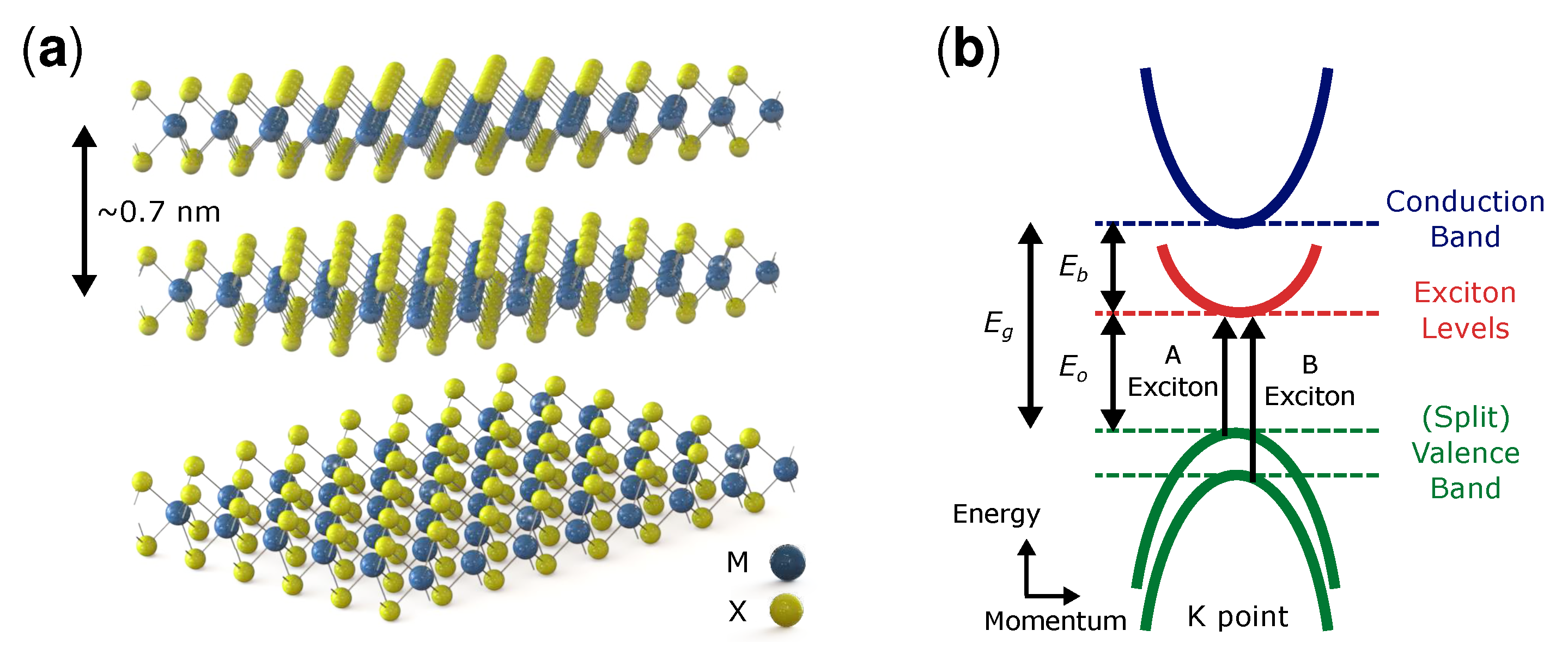
2.1. Fundamental Materials Science

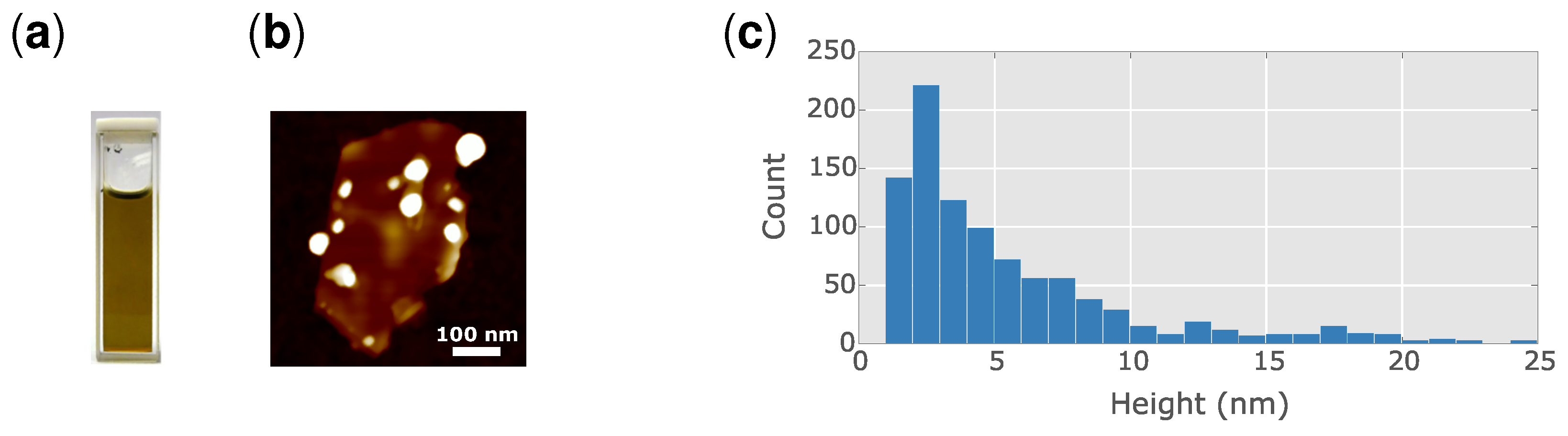
2.2. Fabrication Techniques

2.3. Nonlinear Optical Properties
2.3.1. Saturable Absorption

2.3.2. Origin of Sub-Bandgap Saturable Absorption
2.3.3. Other Nonlinear Effects
3. Pulsed Fibre Lasers Using 2D Materials
3.1. Q-Switched Fibre Lasers

3.2. Mode-Locked Fibre Lasers

4. Outlook
Acknowledgements
Author Contributions
Conflicts of Interest
References
- Okhotnikov, O.G. Fibre Lasers; Wiley: Berlin, Germany, 2012. [Google Scholar]
- Keller, U. Recent developments in compact ultrafast lasers. Nature 2003, 424, 831–838. [Google Scholar] [CrossRef] [PubMed]
- Soffer, B.H. Giant pulse laser operation by a passive, reversibly bleachable absorber. J. Appl. Phys. 1964, 35, 2551. [Google Scholar] [CrossRef]
- Bret, G.; Gires, F. Giant-pulse laser and light amplifier using variable transmission coefficient glasses as light switches. Appl. Phys. Lett. 1964, 4, 175–176. [Google Scholar] [CrossRef]
- Maiman, T.H. Stimulated optical radiation in ruby. Nature 1960, 187, 493–494. [Google Scholar] [CrossRef]
- Ippen, E.P.; Shank, C.V.; Dienes, A. Passive mode locking of the cw dye laser. Appl. Phys. Lett. 1972, 21, 348–350. [Google Scholar] [CrossRef]
- Dzhibladze, M.I.; Esiashvili, Z.G.; Teplitskit, E.S.; Isaev, S.K.; Sagaradze, V.R. Mode locking in a fibre laser. Sov. J. Quantum Electron. 1983, 13, 245–247. [Google Scholar] [CrossRef]
- Zirngibl, M.; Stulz, L.W.; Stone, J.; Hugi, J.; DiGiovanni, D.J.; Hansen, P.B. 1.2 ps pulses from passively mode-locked laser diode pumped Er-doped fibre ring laser. Electron. Lett. 1991, 27, 1734–1735. [Google Scholar] [CrossRef]
- Keller, U.; Miller, D.A.B.; Boyd, G.D.; Chiu, T.H.; Ferguson, J.F.; Asom, M.T. Solid-state low-loss intracavity saturable absorber for Nd:YLF lasers: An antiresonant semiconductor Fabry-Perot saturable absorber. Opt. Lett. 1992, 17, 505–507. [Google Scholar] [CrossRef] [PubMed]
- Novoselov, K.S.; Jiang, D.; Schedin, F.; Booth, T.J.; Khotkevich, V.V.; Morozov, S.V.; Geim, A.K. Two-dimensional atomic crystals. Proc. Natl. Acad. Sci. USA 2005, 102, 10451–10453. [Google Scholar] [CrossRef] [PubMed]
- Wang, Q.H.; Kalantar-Zadeh, K.; Kis, A.; Coleman, J.N.; Strano, M.S. Electronics and optoelectronics of two-dimensional transition metal dichalcogenides. Nat. Nanotechnol. 2012, 7, 699–712. [Google Scholar] [CrossRef] [PubMed]
- Guerreiro, P.T.; Ten, S.; Borrelli, N.F.; Butty, J.; Jabbour, G.E.; Peyghambarian, N. PbS quantum-dot doped glasses as saturable absorbers for mode locking of a Cr: Forsterite laser. Appl. Phys. Lett. 1997, 71, 1595–1597. [Google Scholar] [CrossRef]
- Set, S.; Yaguchi, H.; Tanaka, Y.; Jablonski, M. Ultrafast fibre pulsed lasers incorporating carbon nanotubes. IEEE J. Sel. Top. Quantum Electron. 2004, 10, 137–146. [Google Scholar] [CrossRef]
- Bao, Q.; Zhang, H.; Wang, Y.; Ni, Z.; Yan, Y.; Shen, Z.X.; Loh, K.P.; Tang, D.Y. Atomic-layer graphene as a saturable absorber for ultrafast pulsed lasers. Adv. Funct. Mater. 2009, 19, 3077–3083. [Google Scholar] [CrossRef]
- Hasan, T.; Sun, Z.; Wang, F.; Bonaccorso, F.; Tan, P.H.; Rozhin, A.G.; Ferrari, A.C. Nanotube-polymer composites for ultrafast photonics. Adv. Mater. 2009, 21, 3874–3899. [Google Scholar] [CrossRef]
- Martinez, A.; Sun, Z. Nanotube and graphene saturable absorbers for fibre lasers. Nat. Photonics 2013, 7, 842–845. [Google Scholar] [CrossRef]
- Xia, F.; Wang, H.; Jia, Y. Rediscovering black phosphorus as an anisotropic layered material for optoelectronics and electronics. Nat. Commun. 2014, 5. [Google Scholar] [CrossRef] [PubMed]
- Zhang, Y.; He, K.; Chang, C.Z.; Song, C.L.; Wang, L.L.; Chen, X.; Jia, J.F.; Fang, Z.; Dai, X.; Shan, W.Y.; et al. Crossover of the three-dimensional topological insulator Bi2Te3 to the two-dimensional limit. Nat. Physics 2010, 6, 584–588. [Google Scholar] [CrossRef]
- Geim, A.K.; Grigorieva, I.V. Van der Waals heterostructures. Nature 2013, 499, 419–425. [Google Scholar] [CrossRef] [PubMed]
- Lin, Y.H.; Lin, S.F.; Chi, Y.C.; Wu, C.L.; Cheng, C.H.; Tseng, W.H.; He, J.H.; Wu, C.I.; Lee, C.K.; Lin, G.R. Using n- and p-type Bi2Te3 topological insulator nanoparticles to enable controlled femtosecond mode-locking of fibre lasers. ACS Photonics 2015, 2, 481–490. [Google Scholar] [CrossRef]
- Lee, E.J.; Choi, S.Y.; Jeong, H.; Park, N.H.; Yim, W.; Kim, M.H.; Park, J.K.; Son, S.; Bae, S.; Kim, S.J.; et al. Active control of all-fibre graphene devices with electrical gating. Nat. Commun. 2015, 6. [Google Scholar] [CrossRef] [PubMed]
- Wilson, J.A.; Yoffe, A. The transition metal dichalcogenides: Discussion and interpretation of the observed optical, electrical and structural properties. Adv. Phys. 1969, 18, 193–335. [Google Scholar] [CrossRef]
- Frindt, R.F. Optical absorption of a few unit-cell layers of MoS2. Phys. Rev. 1965, 140, A536–A539. [Google Scholar] [CrossRef]
- Mak, K.F.; Lee, C.; Hone, J.; Shan, J.; Heinz, T.F. Atomically thin MoS2: A new direct-gap semiconductor. Phys. Rev. Lett. 2010, 105, 136805–136811. [Google Scholar] [CrossRef] [PubMed]
- Tongay, S.; Zhou, J.; Ataca, C.; Lo, K.; Matthews, T.S.; Li, J.; Grossman, J.C.; Wu, J. Thermally driven crossover from indirect toward direct bandgap in 2D semiconductors: MoSe2 versus MoS2. Nano Lett. 2012, 12, 5576–5580. [Google Scholar] [CrossRef] [PubMed]
- Kuc, A.; Zibouche, N.; Heine, T. Influence of quantum confinement on the electronic structure of the transition metal sulfide TS2. Phys. Rev. B 2011, 83. [Google Scholar] [CrossRef]
- Yu, P.Y.; Cardona, M. Fundamentals of Semiconductors: Physics and Materials Properties; Springer: Berlin, Germany, 2010. [Google Scholar]
- Kasap, S.; Capper, P. Springer Handbook of Electronic and Photonic Materials; Springer: Berlin, Germany, 2006. [Google Scholar]
- Bonaccorso, F.; Lombardo, A.; Hasan, T.; Sun, Z.; Colombo, L.; Ferrari, A.C. Production and processing of graphene and 2D crystals. Mater. Today 2012, 15, 564–589. [Google Scholar] [CrossRef]
- Woodward, R.I.; Howe, R.C.T.; Hu, G.; Torrisi, F.; Zhang, M.; Hasan, T.; Kelleher, E.J.R. Few-layer MoS2 saturable absorbers for short-pulse laser technology: current status and future perspectives [Invited]. Photonics Res. 2015, 3, A30–A42. [Google Scholar] [CrossRef]
- Howe, R.C.T.; Hu, G.; Yang, Z.; Hasan, T. Functional inks of graphene, metal dichalcogenides and black phosphorus for photonics and (opto)electronics. In Proceeding of Low-Dimensional Materials and Devices, San Diego, CA, USA, 9 August 2015.
- Woodward, R.I.; Kelleher, E.J.R.; Howe, R.C.T.; Hu, G.; Torrisi, F.; Hasan, T.; Popov, S.V.; Taylor, J.R. Tunable Q-switched fibre laser based on saturable edge-state absorption in few-layer molybdenum disulfide (MoS2). Opt. Express 2014, 22, 31113–31122. [Google Scholar] [CrossRef] [PubMed]
- Zhang, H.; Lu, S.B.; Zheng, J.; Du, J.; Wen, S.C.; Tang, D.Y.; Loh, K.P. Molybdenum disulfide (MoS2) as a broadband saturable absorber for ultra-fast photonics. Opt. Express 2014, 22, 7249–7260. [Google Scholar] [CrossRef] [PubMed]
- Xia, H.; Li, H.; Lan, C.; Li, C.; Zhang, X.; Zhang, S.; Liu, Y. Ultrafast erbium-doped fibre laser mode-locked by a CVD-grown molybdenum disulfide (MoS2) saturable absorber. Opt. Express 2014, 22, 17341–17348. [Google Scholar] [CrossRef] [PubMed]
- Li, H.; Xia, H.; Lan, C.; Li, C.; Zhang, X.; Li, J.; Liu, Y. Passively Q-switched erbium-doped fibre laser based on few-layer MoS2 saturable absorber. IEEE Photonics Technol. Lett. 2015, 27, 69–72. [Google Scholar] [CrossRef]
- Khazaeinezhad, R.; Kassani, S.H.; Nazari, T.; Jeong, H.; Kim, J.; Choi, K.; Lee, J.U.; Kim, J.H.; Cheong, H.; Yeom, D.I.; et al. Saturable optical absorption in MoS2 nano-sheet optically deposited on the optical fibre facet. Opt. Commun. 2015, 335, 224–230. [Google Scholar] [CrossRef]
- Zhang, M.; Howe, R.C.T.; Woodward, R.I.; Kelleher, E.J.R.; Torrisi, F.; Hu, G.; Popov, S.V.; Taylor, J.R.; Hasan, T. Solution processed MoS2-PVA composite for sub-bandgap mode-locking of a wideband tunable ultrafast Er:fibre laser. Nano Res. 2015, 8, 1522–1534. [Google Scholar] [CrossRef]
- Woodward, R.I.; Kelleher, E.J.R.; Runcorn, T.H.; Popov, S.V.; Torrisi, F.; Howe, R.C.T.; Hasan, T. Q-switched fibre laser with MoS2 saturable absorber. In CLEO:2014, OSA Technical Digest; Optical Society of America: San Jose, CA, USA, 2014; p. SM3H.6. [Google Scholar]
- Liu, H.; Luo, A.P.; Wang, F.Z.; Tang, R.; Liu, M.; Luo, Z.C.; Xu, W.C.; Zhao, C.J.; Zhang, H. Femtosecond pulse erbium-doped fibre laser by a few-layer MoS2 saturable absorber. Opt. Lett. 2014, 39, 4591–4594. [Google Scholar] [CrossRef] [PubMed]
- Luo, Z.; Huang, Y.; Zhong, M.; Li, Y.; Wu, J.; Xu, B.; Xu, H.; Cai, Z.; Peng, J.; Weng, J. 1-, 1.5-, and 2-μm fibre lasers Q-switched by a broadband few-layer MoS2 saturable absorber. J. Lightwave Technol. 2014, 32, 4679–4686. [Google Scholar] [CrossRef]
- Huang, Y.; Luo, Z.; Li, Y.; Zhong, M.; Xu, B.; Che, K.; Xu, H.; Cai, Z.; Peng, J.; Weng, J. Widely-tunable, passively Q-switched erbium-doped fibre laser with few-layer MoS2 saturable absorber. Opt. Express 2014, 22, 25258–25266. [Google Scholar] [CrossRef] [PubMed]
- Chen, B.; Zhang, X.; Wu, K.; Wang, H.; Wang, J.; Chen, J. Q-switched fibre laser based on transition metal dichalcogenides MoS2, MoSe2, WS2, and WSe2. Opt. Express 2015, 23, 26723–26737. [Google Scholar] [CrossRef] [PubMed]
- Howe, R.C.T.; Woodward, R.I.; Hu, G.; Yang, Z.; Kelleher, E.J.R.; Hasan, T. Surfactant-aided exfoliation of molydenum disulphide for ultrafast pulse generation through edge-state saturable absorption. Available online: http://arxiv.org/abs/1508.01631 (accessed on 26 November 2015).
- Du, J.; Wang, Q.; Jiang, G.; Xu, C.; Zhao, C.; Xiang, Y.; Chen, Y.; Wen, S.; Zhang, H. Ytterbium-doped fibre laser passively mode locked by few-layer molybdenum disulfide (MoS2) saturable absorber functioned with evanescent field interaction. Sci. Rep. 2014, 4. [Google Scholar] [CrossRef] [PubMed]
- Khazaeizhad, R.; Kassani, S.H.; Jeong, H.; Yeom, D.I.; Oh, K. Mode-locking of Er-doped fibre laser using a multilayer MoS2 thin film as a saturable absorber in both anomalous and normal dispersion regimes. Opt. Express 2014, 22, 23732–23742. [Google Scholar] [CrossRef] [PubMed]
- Liu, M.; Zheng, X.W.; Qi, Y.L.; Liu, H.; Luo, A.P.; Luo, Z.C.; Xu, W.C.; Zhao, C.J.; Zhang, H. Microfibre-based few-layer MoS2 saturable absorber for 2.5 GHz passively harmonic mode-locked fibre laser. Opt. Express 2014, 22, 22841–22846. [Google Scholar] [CrossRef] [PubMed]
- Wang, K.; Wang, J.; Fan, J.; Lotya, M.; O’Neill, A.; Fox, D.; Feng, Y.; Zhang, X.; Jiang, B.; Zhao, Q.; et al. Ultrafast saturable absorption of two-dimensional MoS2 nanosheets. ACS Nano 2013, 7, 9260–9267. [Google Scholar] [CrossRef] [PubMed]
- Ren, J.; Wang, S.; Cheng, Z.; Yu, H.; Zhang, H.; Mei, L.; Wang, P. Passively Q-switched nanosecond erbium-doped fibre laser with MoS2 saturable absorber. Opt. Express 2015, 23, 29516–29522. [Google Scholar] [CrossRef] [PubMed]
- Tian, Z.; Wu, K.; Kong, L.; Yang, N.; Wang, Y.; Chen, R.; Hu, W.; Xu, J.; Tang, Y. Mode-locked thulium fibre laser with MoS2. Laser Physics Lett. 2015, 12. [Google Scholar] [CrossRef]
- Zhang, M.; Hu, G.; Hu, G.; Howe, R.C.T.; Chen, L.; Zheng, Z.; Hasan, T. Yb- and Er-doped fibre laser Q-Switched with an optically uniform, broadband WS2 saturable absorber. Available online: http://arxiv.org/abs/1507.03188 (accessed on 26 November 2015).
- Jung, M.; Lee, J.; Park, J.; Koo, J.; Jhon, Y.M.; Lee, H. Mode-locked, 1.94-μm, all-fibreized laser using WS2-based evanescent field interaction. Opt. Express 2015, 23, 241–243. [Google Scholar] [CrossRef] [PubMed]
- Mao, D.; Wang, Y.; Ma, C.; Han, L.; Jiang, B.; Gan, X.; Hua, S.; Zhang, W.; Mei, T.; Zhao, J. WS2 mode-locked ultrafast fibre laser. Sci. Rep. 2015, 5. [Google Scholar] [CrossRef] [PubMed]
- Mao, D.; Zhang, S.; Wang, Y.; Gan, X.; Zhang, W.; Mei, T.; Wang, Y.; Wang, Y.; Zeng, H.; Zhao, J. WS2 saturable absorber for dissipative soliton mode locking at 1.06 and 1.55 μm. Opt. Express 2015, 23, 27509–27519. [Google Scholar] [CrossRef] [PubMed]
- Yan, P.; Liu, A.; Chen, Y.; Chen, H.; Ruan, S.; Chen, S.; Li, I.L.; Yang, H.; Hu, J.; Cao, G. Microfibre-based WS2-film saturable absorber for ultra-fast photonics. Opt. Mater. Express 2015, 5, 479–489. [Google Scholar] [CrossRef]
- Woodward, R.I.; Howe, R.C.T.; Runcorn, T.H.; Hu, G.; Torrisi, F.; Kelleher, E.J.R.; Hasan, T. Wideband saturable absorption in few-layer molybdenum diselenide (MoSe2) for Q-switching Yb-, Er- and Tm-doped fibre lasers. Opt. Express 2015, 23, 1–11. [Google Scholar] [CrossRef] [PubMed]
- Luo, Z.; Li, Y.; Zhong, M.; Huang, Y.; Wan, X.; Peng, J.; Weng, J. Nonlinear optical absorption of few-layer molybdenum diselenide (MoSe2) for passively mode-locked soliton fibre laser [Invited]. Photonics Res. 2015, 3, A79–A86. [Google Scholar] [CrossRef]
- Roxlo, C.B.; Daage, M.; Rupper, A.F.; Chianelli, R.R. Optical absorption and catalytic activity of molybdenum sulfide edge surfaces. J. Catal. 1986, 100, 176–184. [Google Scholar] [CrossRef]
- Zhou, W.; Zou, X.; Najmaei, S.; Liu, Z.; Shi, Y.; Kong, J.; Lou, J.; Ajayan, P.M.; Yakobson, B.I.; Idrobo, J.C. Intrinsic structural defects in monolayer molybdenum disulfide. Nano Lett. 2013, 13, 2615–2622. [Google Scholar] [CrossRef] [PubMed]
- Wang, S.; Yu, H.; Zhang, H.; Wang, A.; Zhao, M.; Chen, Y.; Mei, L.; Wang, J. Broadband few-layer MoS2 saturable absorbers. Adv. Mater. 2014, 26, 3538–3544. [Google Scholar] [CrossRef] [PubMed]
- Zhou, K.G.; Zhao, M.; Chang, M.J.; Wang, Q.; Wu, X.Z.; Song, Y.; Zhang, H.L. Size-dependent nonlinear optical properties of atomically thin transition metal dichalcogenide nanosheets. Small 2015, 11, 694–701. [Google Scholar] [CrossRef] [PubMed]
- Thoen, E.R.; Koontz, E.M.; Joschko, M.; Langlois, P.; Schibli, T.R.; Kaertner, F.X.; Ippen, E.P.; Kolodziejski, L.A. Two-photon absorption in semiconductor saturable absorber mirrors. Appl. Phys. Lett. 1999, 74, 3927–3929. [Google Scholar] [CrossRef]
- Wang, K.; Feng, Y.; Chang, C.; Zhan, J.; Wang, C.; Zhao, Q.; Coleman, J.N.; Zhang, L.; Blau, W.; Wang, J. Broadband ultrafast nonlinear absorption and nonlinear refraction of layered molybdenum dichalcogenide semiconductors. Nanoscale 2014, 6, 10530–10535. [Google Scholar] [CrossRef] [PubMed]
- Popa, D.; Sun, Z.; Hasan, T.; Torrisi, F.; Wang, F.; Ferrari, A.C. Graphene Q-switched, tunable fibre laser. Appl. Phys. Lett. 2011, 98, 1–3. [Google Scholar] [CrossRef]
- Chen, M.; Meng, Z.; Tu, X.; Zhou, H. Low-noise, single-frequency, single-polarization Brillouin/erbium fibre laser. Opt. Lett. 2013, 38, 2041–2043. [Google Scholar] [CrossRef] [PubMed]
- Chen, Y.; Jiang, G.; Chen, S.; Guo, Z.; Yu, X.; Zhao, C.; Zhang, H.; Bao, Q.; Wen, S.; Tang, D.; et al. Mechanically exfoliated black phosphorus as a new saturable absorber for both Q-switching and Mode-locking laser operation. Opt. Express 2015, 23, 12823–12833. [Google Scholar] [CrossRef] [PubMed]
- Wu, K.; Zhang, X.; Wang, J.; Li, X.; Chen, J. WS2 as a saturable absorber for ultrafast photonic applications of mode-locked and Q-switched lasers. Opt. Express 2015, 23, 11453–11461. [Google Scholar] [CrossRef] [PubMed]
- Kassani, S.H.; Khazaeizhad, R.; Jeong, H.; Nazari, T.; Yeom, D.I.; Oh, K. All-fibre Er-doped Q-Switched laser based on Tungsten Disulfide saturable absorber. Opt. Mater. Express 2015, 5, 373–379. [Google Scholar] [CrossRef]
- Svelto, O. Principles of Lasers; Springer: Berlin, Germany, 2010. [Google Scholar]
- Sobon, G. Mode-locking of fibre lasers using novel two-dimensional nanomaterials: Graphene and topological insulators [Invited]. Photonics Res. 2015, 3, A56–A63. [Google Scholar] [CrossRef]
- Zhao, C.; Zhang, H.; Qi, X.; Chen, Y.; Wang, Z.; Wen, S.; Tang, D. Ultra-short pulse generation by a topological insulator based saturable absorber. Appl. Phys. Lett. 2012, 101. [Google Scholar] [CrossRef]
- Sotor, J.; Sobon, G.; Macherzynski, W.; Paletko, P.; Grodecki, K.; Abramski, K.M. Mode-locking in Er-doped fibre laser based on mechanically exfoliated Sb2Te3 saturable absorber. Opt. Mater. Express 2014, 4, 1–6. [Google Scholar] [CrossRef]
- Sotor, J.; Sobon, G.; Macherzynski, W.; Paletko, P.; Abramski, K.M. Black phosphorus—A new saturable absorber material for ultrashort pulse generation. Available online: http://arxiv.org/ftp/arxiv/papers/1504/1504.04731.pdf (accessed on 26 November 2015).
- Wu, K.; Zhang, X.; Wang, J.; Chen, J. 463-MHz fundamental mode-locked fibre laser based on few-layer MoS2 saturable absorber. Opt. Lett. 2015, 40, 1374–1377. [Google Scholar] [CrossRef] [PubMed]
- Chong, A.; Buckley, J.; Renninger, W.; Wise, F. All-normal-dispersion femtosecond fibre laser. Opt. Express 2006, 14, 10095–10100. [Google Scholar] [CrossRef] [PubMed]
- Zhang, W.; Chuu, C.P.; Huang, J.K.; Chen, C.H.; Tsai, M.L.; Chang, Y.H.; Liang, C.T.; Chen, Y.Z.; Chueh, Y.L.; He, J.H.; et al. Ultrahigh-gain photodetectors based on atomically thin graphene-MoS2 heterostructures. Sci. Rep. 2014, 4. [Google Scholar] [CrossRef] [PubMed]
- Wang, Y.; Mao, D.; Gan, X.; Han, L.; Ma, C.; Xi, T.; Zhang, Y.; Shang, W.; Hua, S.; Zhao, J. Harmonic mode locking of bound-state solitons fibre laser based on MoS2 saturable absorber. Opt. Express 2015, 23, 205–210. [Google Scholar] [CrossRef] [PubMed]
- Lefrançois, S.; Kieu, K.; Deng, Y.; Kafka, J.D.; Wise, F.W. Scaling of dissipative soliton fibre lasers to megawatt peak powers by use of large-area photonic crystal fibre. Opt. Lett. 2010, 35, 1569–1571. [Google Scholar] [CrossRef] [PubMed]
- Woodward, R.I.; Kelleher, E.J.R.; Runcorn, T.H.; Loranger, S.; Popa, D.; Wittwer, V.J.; Ferrari, A.C.; Popov, S.V.; Kashyap, R.; Taylor, J.R. Fibre grating compression of giant-chirped nanosecond pulses from an ultra-long nanotube mode-locked fibre laser. Opt. Lett. 2015, 40, 387–390. [Google Scholar] [CrossRef] [PubMed]
- Wu, D.; Peng, J.; Zhong, Y.; Cheng, Y.; Qu, B.; Weng, J.; Luo, Z.; Xu, B.; Cheng, N.; Xu, H.; et al. 2-D materials-based passively Q-switched 635 nm Pr3+-doped ZBLAN fibre lasers. In Proceedings of Advanced Solid State Lasers Conference, Berlin, Germany, 4–9 October 2015; p. ATu2A.28.
- Tran, V.; Soklaski, R.; Liang, Y.; Yang, L. Layer-controlled band gap and anisotropic excitons in few-layer black phosphorus. Phys. Rev. B 2014, 89. [Google Scholar] [CrossRef]
- Mu, H.; Wang, Z.; Yuan, J.; Xiao, S.; Chen, C.; Chen, Y.; Chen, Y.; Song, J.; Wang, Y.; Xue, Y.; et al. Graphene-Bi2Te3 heterostructure as saturable absorber for short pulse generation. ACS Photonics 2015, 2, 832–841. [Google Scholar] [CrossRef]
© 2015 by the authors; licensee MDPI, Basel, Switzerland. This article is an open access article distributed under the terms and conditions of the Creative Commons Attribution license (http://creativecommons.org/licenses/by/4.0/).
Share and Cite
Woodward, R.I.; Kelleher, E.J.R. 2D Saturable Absorbers for Fibre Lasers. Appl. Sci. 2015, 5, 1440-1456. https://doi.org/10.3390/app5041440
Woodward RI, Kelleher EJR. 2D Saturable Absorbers for Fibre Lasers. Applied Sciences. 2015; 5(4):1440-1456. https://doi.org/10.3390/app5041440
Chicago/Turabian StyleWoodward, Robert I., and Edmund J. R. Kelleher. 2015. "2D Saturable Absorbers for Fibre Lasers" Applied Sciences 5, no. 4: 1440-1456. https://doi.org/10.3390/app5041440
APA StyleWoodward, R. I., & Kelleher, E. J. R. (2015). 2D Saturable Absorbers for Fibre Lasers. Applied Sciences, 5(4), 1440-1456. https://doi.org/10.3390/app5041440