Article

Characterization of Transition Metal Oxide/Silicon Heterojunctions for Solar Cell Applications

Electronic Engineering Department, Polytechnic University of Catalonia, Barcelona 08034, Spain
*
Author to whom correspondence should be addressed.
Current Address: Department of Applied Physics, Indian School of Mines, Dhanbad 826004, India
Appl. Sci. 2015, 5(4), 695-705; https://doi.org/10.3390/app5040695
Submission received: 15 September 2015 / Accepted: 1 October 2015 / Published: 9 October 2015

Abstract

:
During the last decade, transition metal oxides have been actively investigated as hole- and electron-selective materials in organic electronics due to their low-cost processing. In this study, four transition metal oxides (V2O5, MoO3, WO3, and ReO3) with high work functions (>5 eV) were thermally evaporated as front p-type contacts in planar n-type crystalline silicon heterojunction solar cells. The concentration of oxygen vacancies in MoO3−x was found to be dependent on film thickness and redox conditions, as determined by X-ray Photoelectron Spectroscopy. Transfer length method measurements of oxide films deposited on glass yielded high sheet resistances (~109 Ω/sq), although lower values (~104 Ω/sq) were measured for oxides deposited on silicon, indicating the presence of an inversion (hole rich) layer. Of the four oxide/silicon solar cells, ReO3 was found to be unstable upon air exposure, while V2O5 achieved the highest open-circuit voltage (593 mV) and conversion efficiency (12.7%), followed by MoO3 (581 mV, 12.6%) and WO3 (570 mV, 11.8%). A short-circuit current gain of ~0.5 mA/cm2 was obtained when compared to a reference amorphous silicon contact, as expected from a wider energy bandgap. Overall, these results support the viability of a simplified solar cell design, processed at low temperature and without dopants.

Graphical Abstract

1. Introduction

Although crystalline silicon (c-Si) solar cells are a mature technology with competitive energy prices in several markets, efforts toward higher efficiencies, lower costs and lesser environmental impacts continue to lead the photovoltaic community. State of the art technology already allows for low-temperature deposition of dopants (T < 200 °C) in amorphous silicon a-Si:H/c-Si heterojunction devices, but thermally-diffused doping (T > 900 °C) is still the industry standard, covering ~12% of the module fabrication energy input [1]. As advanced solar cell architectures become closer to the theoretical efficiency limits for single-junction devices, further cost reduction must then come from ambient-temperature or solution-based processes and materials.
In parallel, the development of thin-film and dye-sensitized/organic photovoltaics has introduced novel materials with excellent optoelectronic properties that could substitute standard silicon dopants. Such materials have recently been reported in conjunction with p- and n-type c-Si, including organic polymers (PEDOT: PSS [2], P3HT [3]), transparent conductive oxides (ZnO [4]), transition metal oxides (TiO2 [5], MoO3 [6], WO3 [7]) or their combination [8,9], reaching power conversion efficiencies as high as 18.8% [10] for MoO3/n-type c-Si heterojunctions. A distinctive attribute of these materials is their preferential conductivity for one kind of charge carrier (i.e., holes) while blocking the other kind (electrons), aiding in the separation of photogenerated carriers [11]. They are usually wide bandgap semiconductors (highly transparent) with low contact resistivities, although the primary benefit is their processability by low-temperature techniques (vacuum thermal evaporation, atomic layer deposition) or by thin-film coating methods.
This paper explores the use of four transition metal oxides (V2O5, MoO3, WO3, and ReO3) as front p-type contacts in planar n-type crystalline silicon (n-Si) solar cells. The compositional, optical and electrical properties of these oxides will be discussed in terms of the solar cell design, making emphasis on their advantages (optical gains) and disadvantages (post-annealing degradation) when compared to conventional a-Si:H layers.

2. Experimental Details

The oxide/c-Si solar cells were fabricated on double-side polished mono-crystalline (float zone, 100 orientation) n-Si wafers (~2.5 Ωcm, ND ~ 1.8 × 1015 cm−3) of 280 μm thickness. After the standard RCA cleaning process and 1% HF bath (1 min) to remove native SiO2, samples were introduced in a Plasma-Enhanced Chemical Vapor Deposition (PECVD) system (Elettrorava, Turin, Italy) for deposition of three hydrogenated amorphous-silicon carbide layers (a-SiCx:H, 0.2 < x < 1) on the rear side of the wafer. This passivating/n+ doped/reflective stack was then laser-fired (infrared nanosecond laser) to create a matrix of point contacts (0.5% contacted area) with a measured contact resistivity <0.5 mΩcm2 and an effective surface recombination velocity ~50 cm/s (before metallization) [12]. After a second 1% HF bath, the different transition metal oxides (Sigma Aldrich, Dorset, England; 99.99%, powdered) were deposited by vacuum thermal evaporation from a tantalum boat at <8 × 10⁻⁶ mbar at a rate <0.2 Ȧ/s. Even though ReO3 was evaporated without difficulty, the film proved unstable when exposed to ambient air and some of the devices could not be measured. The oxide thickness was fixed at 15 nm and controlled by quartz microbalance. The samples were then briefly exposed to air for transferring into a RF-magnetron sputtering system for deposition of an 80 nm Indium-Tin Oxide (ITO) conductive/anti-reflective layer (ITO target: J.J. Lesker, Hastings, England), followed by lithographic patterning of 1 cm2 cell area. Contacting of the rear side was done by electron-beam assisted evaporation of Ti (15 nm)/Al (1000 nm) followed by a front grid (4.3% shadow) of thermally evaporated Ag (metals: J.J. Lesker, Hastings, England). A reference device was also fabricated by replacing the transition metal oxide layer with an intrinsic (i) a-Si:H (4 nm)/(p) a-Si:H (15 nm) stack contacted by ITO and using the same point contact strategy on the rear side. Figure 1(a) depicts the structure of the oxide/n-Si heterojunction solar cells.
Figure 1. (a) Schematic of the transition metal oxide/n-Si heterojunction solar cell; (b) reported work functions for ReO3 [13], V2O5, MoO3 and WO3 [14]. The valence and conduction band energy levels of c-Si are also shown.
Applsci 05 00695 g001
Characterization of the solar cells was performed before and after a 10 min 160 °C annealing in N2 atmosphere. The current-voltage characteristics were measured (Keithley Instruments 2601B, Cleveland, OH, USA) both in dark and AM1.5g standard illumination (Oriel Instruments, Irvine, CA, USA), extracting the relevant cell performance parameters. The External Quantum Efficiency (EQE) response was measured by a commercial instrument (PV Measurements QEX10, Boulder, CO, USA) and the total reflectance by spectrophotometry (Shimadzu 3600, Kyoto, Japan) with an integrating sphere. Optical simulation of the solar cell structure was done by the tool Wafer Ray Tracer [15] (Version 1.6.4, PV Lighthouse Pty. Ltd., Australia) at 20 nm intervals and 5000 incident rays. Transfer Length Method (TLM) measurements of the oxide films (15 nm thick) were also performed with 1 × 0.1 cm Au electrodes at various distance intervals, measuring the current-voltage response (Keithley Instruments 2636, Cleveland, OH, USA; 1fA resolution) in the dark and under vacuum. The elemental composition of MoO3 films was determined from Gaussian-Lorentzian peak fittings of X-ray Photoelectron Spectroscopy (XPS) spectra measured at <3 × 10⁻⁹ mbar using a non-monochromatic Al-Kα source (SPECS, Berlin, Germany; Phoibos 150 detector).

3. Results and Discussion

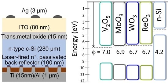
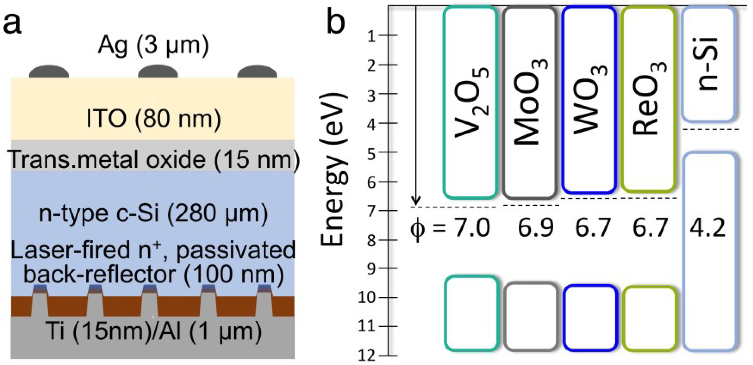
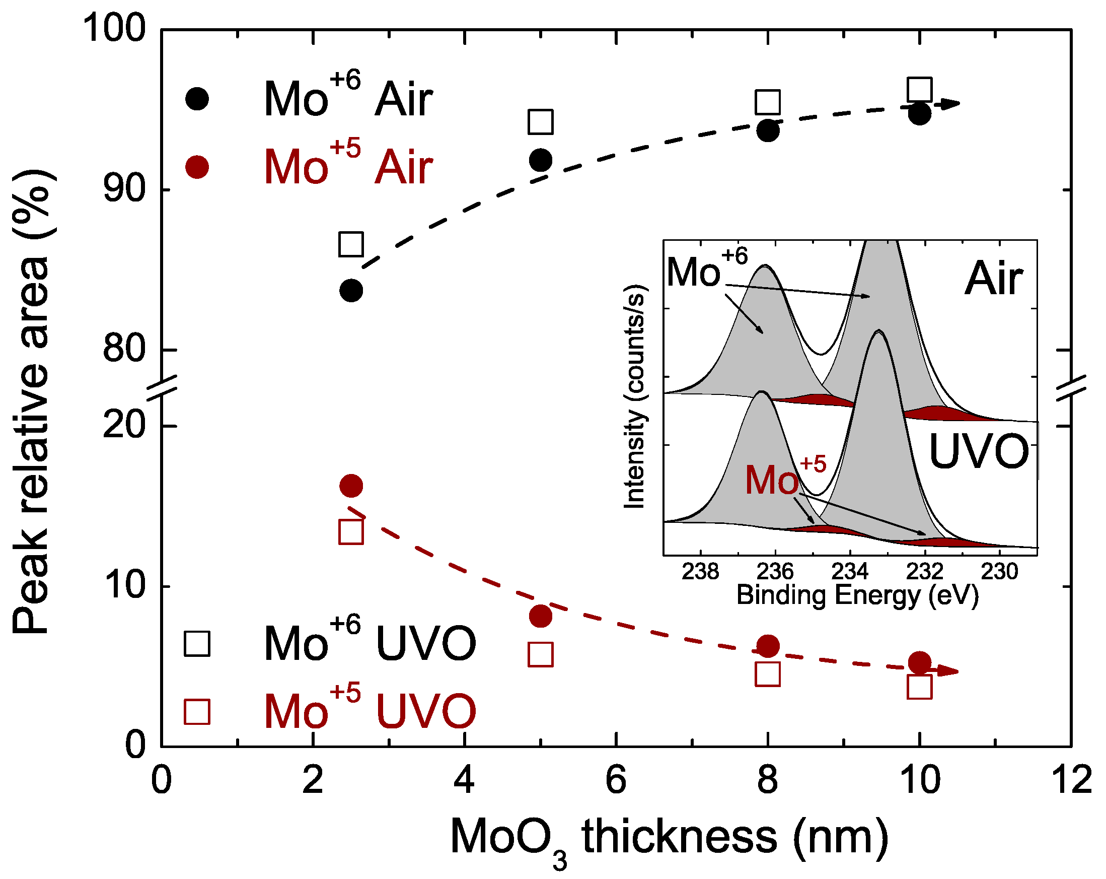
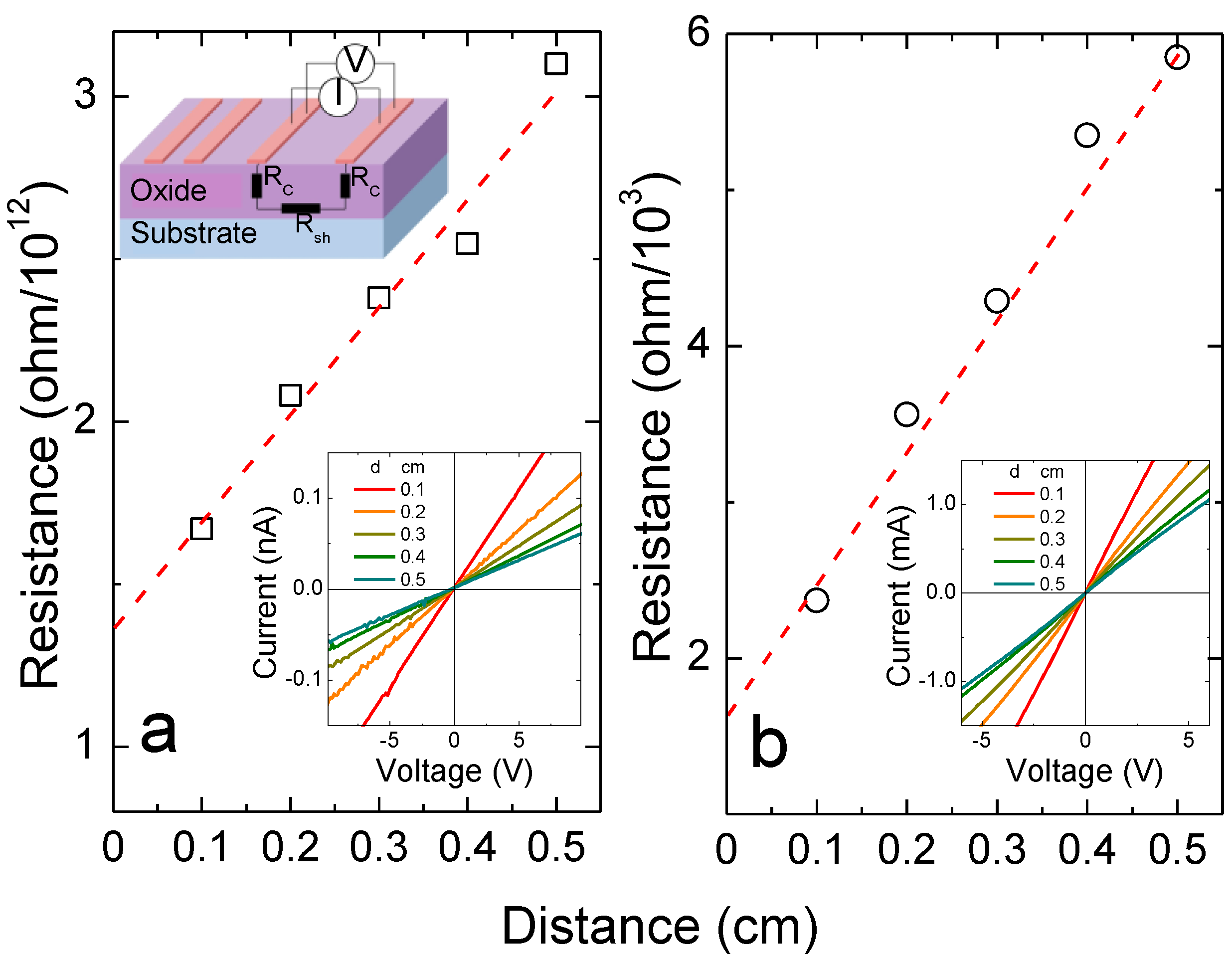
3.1. Transition Metal Oxide Characterization

Transition metal oxides are wide bandgap semiconductors that have been employed as hole and electron transport layers in organic solar cells and light emitting diodes due to their wide range of work functions varying from 3 eV (ZrO2) to 7 eV (V2O5) [16]. Their doping character is determined by defect vacancies in their atomic structure, resulting in either p-type doping for metal vacancies or in n-type doping for oxygen vacancies, as is the case in the four n-type oxides under study (Figure 1(b)) [13,14]. Likewise, the conductivity and work function vary with oxygen content in an inverse manner, shifting from high work function insulators (MoO3) to semiconductors (MoO3−x) to low work function metallic-like conductors (MoO2) as the cation oxidation state decreases (Mo+6 → Mo+5 → Mo+4) [16]. In order to determine the stoichiometry of the prepared samples, Figure 2 shows the elemental content of Mo+6 and Mo+5 cations calculated from the integrated areas of the fitted Mo 3d XPS peaks (inset) for different MoO3 thicknesses and two different post-deposition treatments (air-exposure and UV-ozone, 15 min). For the air-exposed films, it is observed that the Mo+6 content increases with film thickness and stabilizes at a value of ~94%, while the Mo+5 content inversely decreases to ~6%. This phenomenon has been thoroughly investigated for several metallic substrates and has been attributed to thermodynamically driven redox reactions at the MoOx/substrate interface [17]. Similarly, the UV-ozone treated samples follow the same trend but with a larger Mo+6 content due to ozone oxidation, stabilizing at a value of ~96% (~4% for Mo+5). By integrating the fitted O 2p peaks, average oxygen to metal (O/M) ratios were calculated at MoO2.5 (air-exposed) and MoO2.6 (UV-ozone). Oxygen deficiency has also been reported for thermally evaporated V2O5 [18], WO3 [7] and ReO3 [13], which allows for fine-tuning of the desired work function by means of different process conditions and post-deposition treatments [19,20].
Figure 2. Relative content of Mo+6 and Mo+5 oxidation states for different MoO3 film thicknesses (2.5, 5, 8 and 10 nm) and post-deposition treatments (air exposure and ultraviolet light ozone—UVO). Inset shows the fitted XPS spectra for both Mo 3d states identified (8 nm). Lines are a guide to the eye.
Applsci 05 00695 g002
Even if variations in composition allow for enhancements in conductivity, transition metal oxides are in general poor conductors when compared to doped silicon or transparent conductive oxides. To determine the electrical properties of the evaporated MoO3 films, the Transfer Length Method (TLM) results were analyzed to extract the sheet resistance (Rsh), both in glass and n-Si substrates, according to the relation [21]:
R T = 2 R C +   ( R S h W ) d
where RT is the total resistance measured between two electrodes of width W separated by a distance d, while 2RC is the transversal contact resistance between Au/MoO3 (glass sample) and Au/MoO3/n-Si (n-Si sample). Figure 3 plots the dark RT measurements at increasing d intervals for both samples, obtaining a sheet resistance of ~5 × 10¹² Ω/sq for MoO3/glass and ~1 × 10⁴ Ω/sq for MoO3/n-Si. The large difference between both measurements is explained by the formation of an inversion layer on silicon’s surface, acting as p-type contacts in the n-Si substrate [10,22]. Note also that Rsh for the n-Si substrate (with ~2.5 Ωcm resistivity) is ~65 Ω/sq and does not contribute significantly to the inversion layer resistance. Similar results were obtained for V2O5 and WO3 deposited on glass and n-Si substrates (Table 1), indicating the formation of an inversion layer. Also, MoO3 samples yielded a 3% higher Rsh when treated with UV-ozone, as expected from a higher Mo+6 content.
Figure 3. Transfer length method measurements of 15 nm thick MoO3 films deposited on (a) glass and (b) n-Si, measured with 40 nm Au electrodes. Insets show the current-voltage measurements at different distance intervals d.
Applsci 05 00695 g003
Due to the high sheet resistance values discussed above, a transparent conductive oxide is required for current collection, so that the main contribution of the inversion layer (IL) to the cell series resistance comes from the transversal current flow across the IL/oxide/ITO interfaces, which can be approximated from the contact resistivity ρC = RC AT (where AT is the effective current flow area). However, the obtained contact resistivities were overestimated due to the large errors inherent to the TLM itself [21], being inconsistent with the series resistances and fill factors measured in the finished solar cells and needing further analysis.
Table 1. Sheet resistance (Rsh) of the oxides calculated from the transfer length method (TLM). The ReO3 device was not measured due to film instabilities.
Oxide Sheet Resistance (Rsh), Ω/sq
Glass substrateSilicon substrate
V2Ox3.3 × 1095.8 × 103
MoOx5 × 10121.0 × 104
WOx1.1 × 1091.2 × 105
Figure 4. (a) Simulated photocurrent density (Jph) of the planar solar cell as a function of MoO3 and Indium-Tin Oxide (ITO) layer thickness, achieving a maximum photocurrent of 35.7 mA/cm2 for 80 nm ITO and 15 nm MoO3. (b) Simulated optical losses (in mA/cm2) for MoOx and a-Si:H (15 nm each).
Applsci 05 00695 g004
From the optical perspective, the thicknesses of both ITO and transition metal oxide layers need to be adjusted for an optimum anti-reflection quality. Figure 4(a) shows the maximum photocurrent density Jph for the MoO3/n-Si solar cell simulated with the Wafer Ray Tracer program (AM1.5g solar spectrum), showing an optimum window across the 0–100 nm thickness range. The simulation parameters (refractive index and extinction coefficient) where wavelength dependent and taken from the program material database [15], including MoO3 (alpha-phase) from [23]. Since the sputtered ITO has a moderately high Rsh ~130 Ω/sq, a minimum thickness of 80 nm was fixed in order to limit the resistance losses, yielding a maximum photocurrent of 35.7 mA/cm2 for a MoO3 thickness of 15 nm. This oxide thickness also ensures a uniform coverage of the random pyramids. Furthermore, the large bandgap energy of transition metal oxides (Egap ~3 eV) reduces the absorption losses in comparison to standard a-Si:H (~1.7 eV). Figure 4(b) shows the distribution of the incident current density for both MoO3 and a-Si:H as front window layers, showing the optical losses by reflection and by parasitic absorption (front and rear layers). The larger MoO3 Egap represents a potential gain in photocurrent of ~1.8 mA/cm2, although reflection losses are considerably high and could be lowered to <2.7 mA/cm2 if a texturized wafer is used.

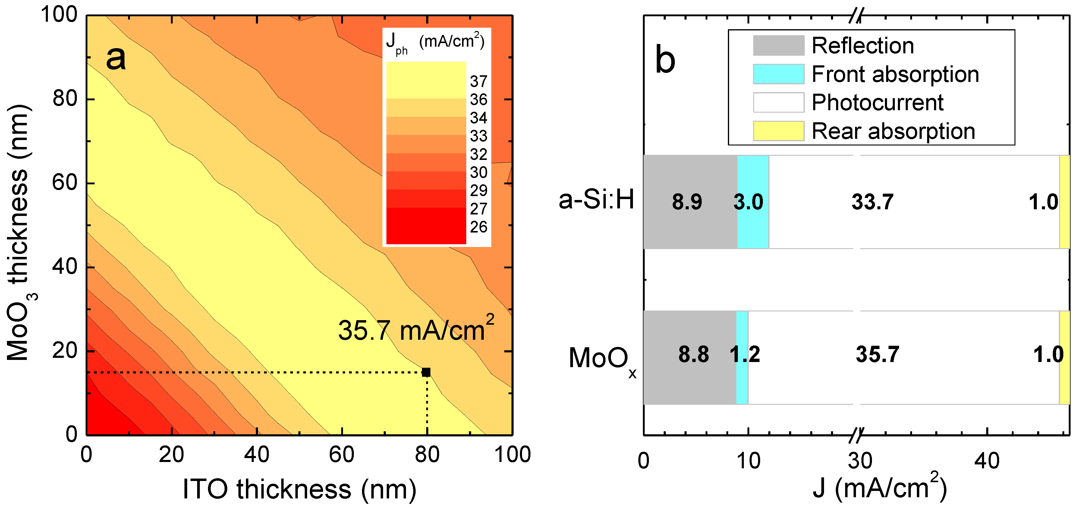
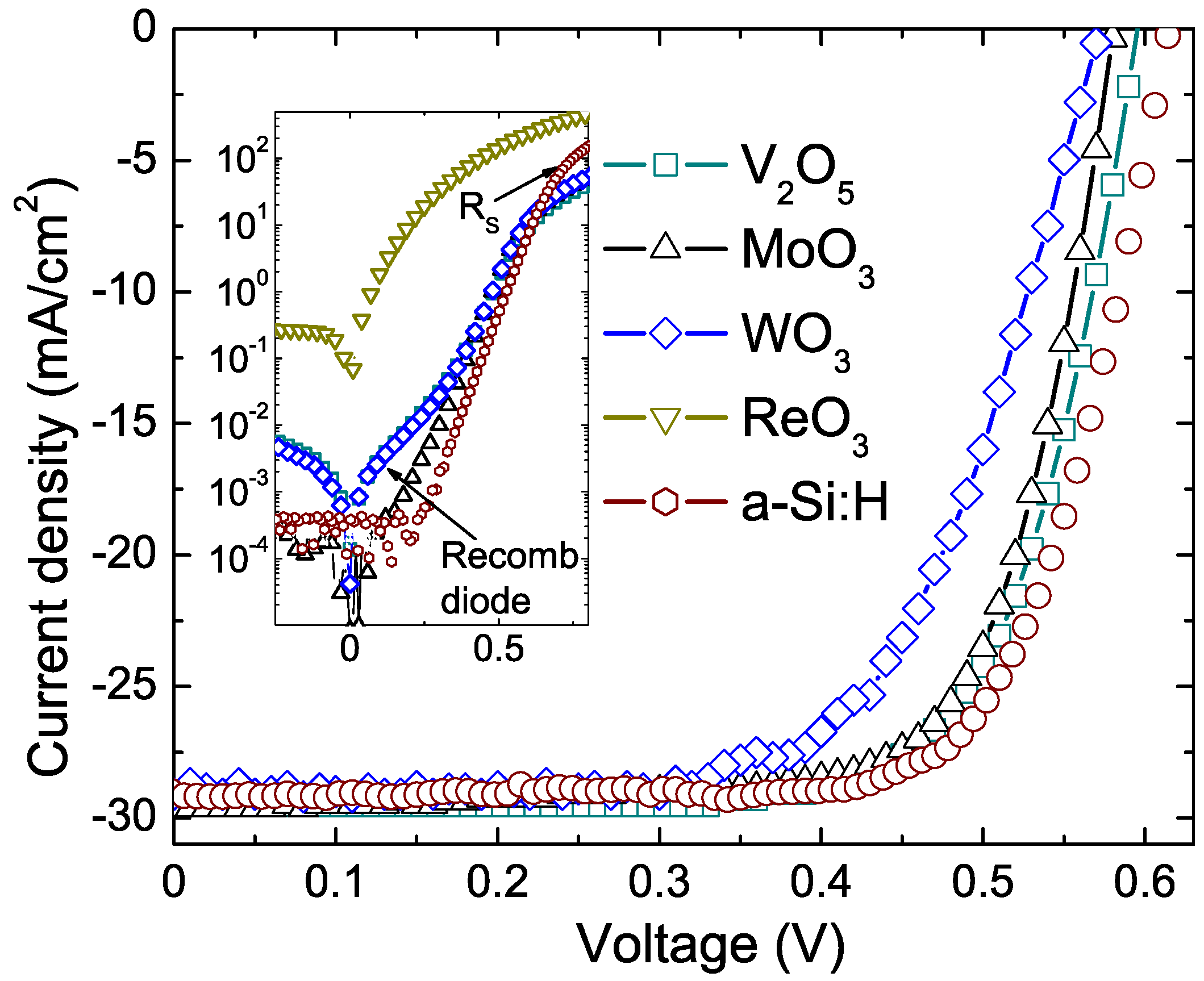
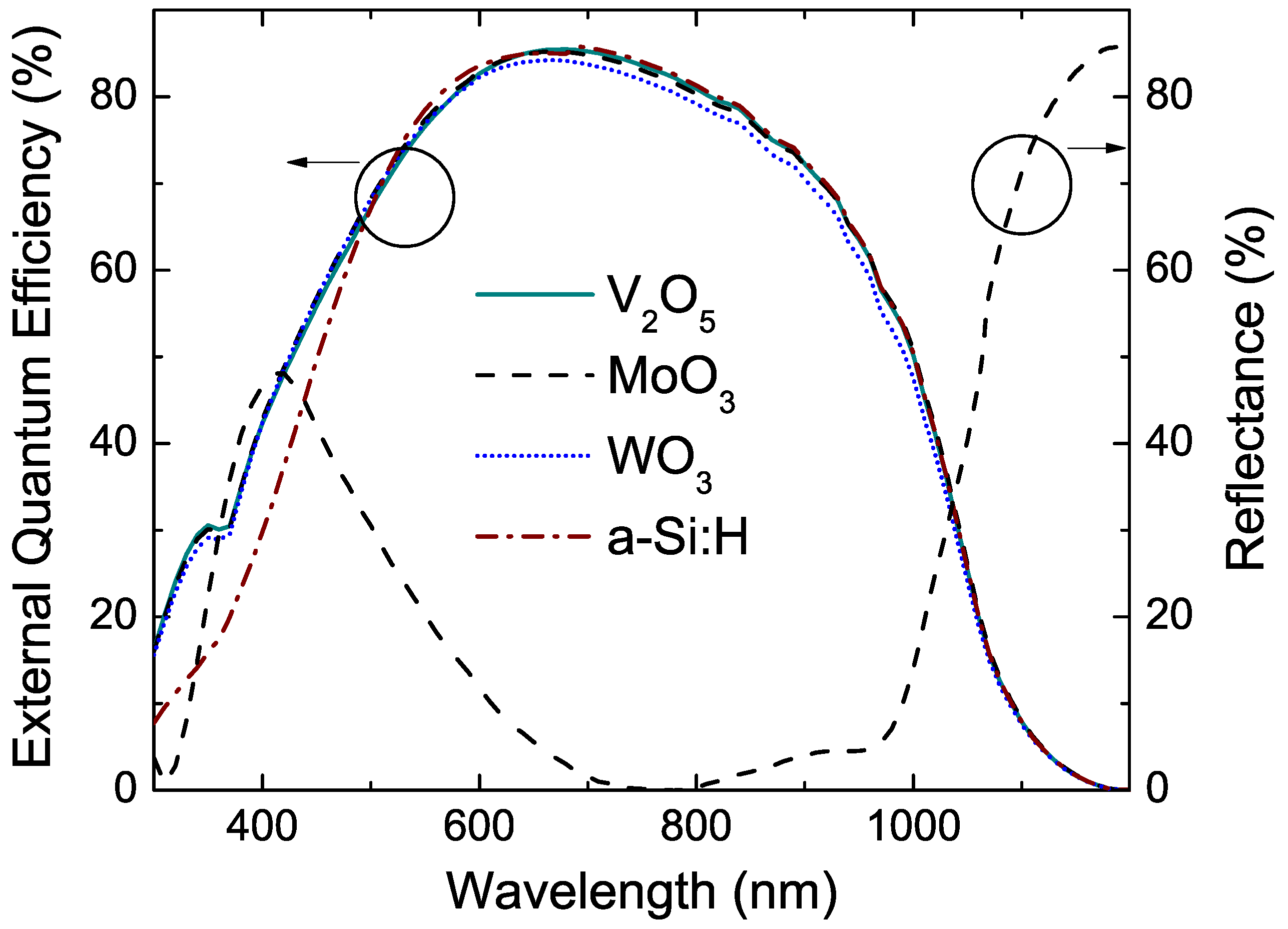
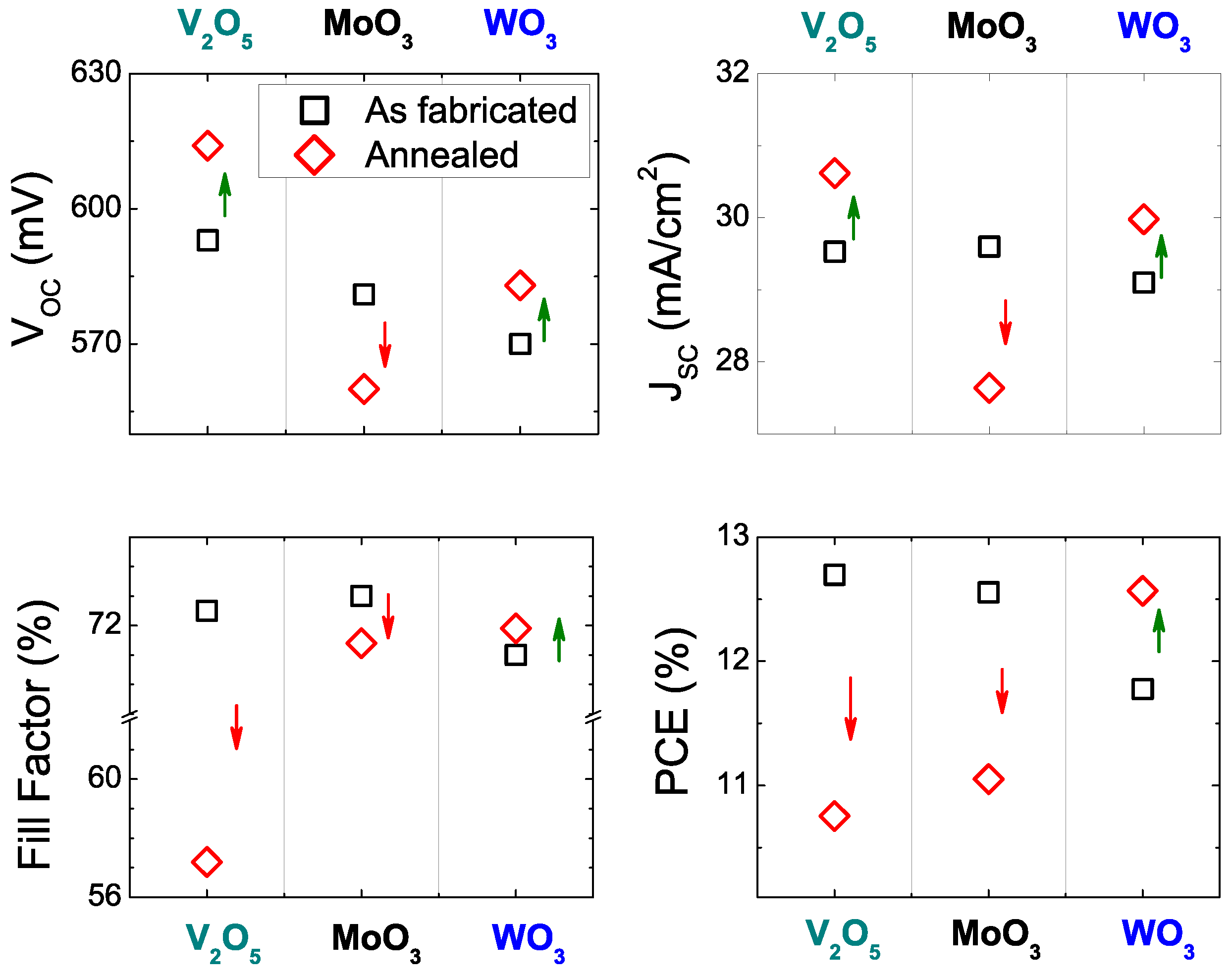
3.2. Solar Cell Characterization

Besides reduced parasitic absorption and moderate resistance losses, transition metal oxides must also generate a potential difference that facilitates the separation of photogenerated carriers. Figure 5 depicts the current density-voltage (J-V) characteristic of the oxide/n-Si solar cells under standard AM1.5g illumination and in the dark (inset). All oxide solar cells show the typical rectifying behavior of a p-n junction except for ReO3, whose surface quality was severely deteriorated and produced a Schottky diode between ITO and silicon. The cell dark response at high voltage shows larger series resistance (RS) than the a-Si:H reference, while at low voltage the so-called recombination diode indicates inadequate passivation of the oxide/n-Si interface. Under illumination, the highest open-circuit voltage (VOC) is achieved by the V2O5 cell with 593 mV, followed by MoO3 (581 mV) and WO3 (570 mV). These VOC values are notable given the chemical dissimilarity between materials, the thinness of the oxide layer and the simple solar cell design, and even though higher VOC s have been reported by use of (i) a-Si:H passivating interlayers [7,10], they introduce an additional processing step (PEVCD). Moreover, a correlation could be inferred between the reported work functions values (Figure 1(b)) and the measured VOC s (with larger work functions exerting a stronger surface inversion on n-Si), but further research is necessary. As to the short-circuit current densities (JSC), all cells achieved a relatively constant value of ~29 mA/cm2, with the reference being slightly lower due to its higher parasitic absorption (lower Egap). The observed Fill Factors (FF) were similar for all cells (>70%) and could be improved by decreasing RS, which is dominated by ITO’s sheet resistance and probably by the high contact resistivity amongst n-Si/oxide/ITO. By considering the obtained solar cell parameters (Table 2), the Power Conversion Efficiencies (PCE) were 12.7% (V2O5), 12.6% (MoO3) and 11.8% (WO3), compared to a reference 13.1%.
Figure 5. Current density-voltage (J-V) response of the fabricated oxide/n-Si solar cells under standard AM1.5g illumination, including an a-Si:H reference device. Inset shows J-V under dark conditions.
Applsci 05 00695 g005
Table 2. Performance parameters of the fabricated oxide/n-Si solar cells and the a-Si:H reference device.
OxidePCE %VOC mVJSC mA/cm2FF %RS Ωcm2
V2O512.759329.672.40.9
MoO312.658129.673.10.8
WO311.857029.171.01.0
ReO33.124528.944.41.1
a-Si:H13.161729.173.00.55
The External Quantum Efficiency (EQE) response of the solar cells is shown in Figure 6. The curves show considerable reflectance losses in the ultraviolet and near-infrared wavelengths, which could be lowered by fabricating the device on a texturized wafer. Likewise, the reflectance minimum (~750 nm) could be shifted to shorter wavelengths by reducing the ITO thickness, matching the solar spectrum power peak (~525 nm) and enhancing photon absorption. A notable feature of the oxide cells is the improved response in the 300–550 nm range when compared to a-Si:H, explained by the lower parasitic absorption of the oxide films and predicted by the optical simulation of the device, accounting for a net gain in JSC of ~0.5 mA/cm2.
Figure 6. External quantum efficiency and total reflectance of the fabricated oxide/n-Si solar cells, including an a-Si:H reference device.
Applsci 05 00695 g006
Finally, it is well known in a-Si:H/c-Si heterojunction technology that ion bombardment occurring during ITO sputtering degrades the passivation of a c-Si surface [24], increasing carrier recombination (lower JSC) and decreasing the effective minority carrier lifetime (lower VOC). A short post-fabrication annealing at 160 °C is sufficient to recover the damage, as evidenced by a VOC and JSC enhancement of the reference a-Si:H cell to 645 mV and 32.7 mA/cm2. In search of a similar boost in performance, the oxide/n-Si cells were annealed under the same conditions, obtaining varied results as summarized in Figure 7. The V2O5 device decreased its PCE to 10.8% as a consequence of a drop in FF, even though its VOC indeed recovered to 614 mV. For the MoO3 cell, its efficiency dropped to 11.0% due to VOC (560 mV) and JSC (27.6%) deterioration. The WO3 cell was the only material that showed a positive improvement in efficiency (12.6%), increasing its VOC and JSC to 583 mV and 30 mA/cm2. Overall, the results suggest that the V2O5 and MoO3 films are strongly sensitive to temperature, although the threshold at which their optical and electric properties degrade still needs to be determined.
Figure 7. Solar cell performance parameters before and after thermal annealing (10 min, 160 °C).
Applsci 05 00695 g007

4. Conclusions

Thermally evaporated transition metal oxides were successfully employed as front p-type contacts in planar n-type c-Si solar cells, achieving VOC values of 593 mV (V2O5), 581 mV (MoO3) and 570 mV (WO3), for a maximum power conversion efficiency of 12.7% (V2O5). XPS analyses of MoO3 films showed a dependence of the cation oxidation state with thickness and an average oxygen deficiency of MoO2.55, while moderate sheet resistance values (104 Ω/sq) of the oxide films deposited on n-Si were attributed to the formation of a surface inversion layer. When compared to a reference a-Si:H layer, a gain in JSC ~0.5 mA/cm2 was seen for the wider bandgap oxide layers, though serious losses in efficiency were observed for the V2O5 and MoO3 cells after thermal annealing treatments. Future studies should focus on enhancing the passivation of the oxide/c-Si interface, avoiding the damage caused by ITO sputtering and lowering the contact resistivity. Lastly, by use of another transition metal oxide layer as rear n-type contact, a simplified solar cell architecture that is dopant-free and fully processed at low temperature could offer important reductions in cost for crystalline silicon photovoltaics.

Acknowledgments

This work was supported by the Spain government under the ENE2013-48629-C4-1-R and ENE2014-56237-C4-1-R projects. The authors would like to thank Thomas Duc (École Polytechnique, Paris) for the optical simulations and the transfer length method measurements, Montserrat Domínguez for the X-ray photoelectron spectroscopy analyses and Anna Morales-Vilches for the reference solar cell. The authors are also thankful for financial support from the Mexican government grants program (CONACyT) and the Erasmus Mundus Action 2 Areas+ grants program.

Author Contributions

L.G.G., C.V. and J.P. conceived and designed the experiments; L.G.G. and S.M. performed the experiments and analyzed the data; R.A. coordinated the equipment and materials; L.G.G. wrote the paper.

Conflicts of Interest

The authors declare no conflict of interest.

References

  1. Alsema, E.A.; de Wild-scholten, M.J. Environmental impacts of crystalline silicon photovoltaic module production. In Proceedings of the 13th CIRP International Conference in Life Cycle Engineering, Leuven, Belgium, 31 May 2006.
  2. Thomas, J.P.; Leung, K.T. Defect-minimized PEDOT: PSS/planar-Si solar cell with very high efficiency. Adv. Funct. Mater. 2014, 24, 4978–4985. [Google Scholar]
  3. Weingarten, M.; Zweipfennig, T.; Vescan, A.; Kalisch, H. Low-temperature processed hybrid organic/silicon solar cells with power conversion efficiency up to 6.5%. MRS Proceedings 2015, 1771. mrss15-2133323. [Google Scholar] [CrossRef]
  4. Hussain, B.; Ebong, A.; Ferguson, I. Zinc oxide as an active n-layer and antireflection coating for silicon based heterojunction solar cell. Sol. Energy Mater. Sol. Cells 2015, 139, 95–100. [Google Scholar] [CrossRef]
  5. Nagamatsu, K.A.; Avasthi, S.; Sahasrabudhe, G.; Man, G.; Jhaveri, J.; Berg, A.H. Titanium dioxide/silicon hole-blocking selective contact to enable double-heterojunction crystalline silicon-based solar cell. Appl. Phys. Lett. 2015, 106, 123906. [Google Scholar] [CrossRef]
  6. Bullock, J.; Yan, D.; Cuevas, A.; Wan, Y.; Samundsett, C. n- and p-type silicon solar cells with molybdenum oxide hole contacts. Energy Procedia 2015, 77, 446–450. [Google Scholar] [CrossRef]
  7. Bivour, M.; Temmler, J.; Steinkemper, H.; Hermle, M. Alternative contact materials for induced junction silicon solar cells. Sol. Energy. Mater. Sol. Cells 2015, 142, 34–41. [Google Scholar] [CrossRef]
  8. Liu, R.; Lee, S.T.; Sun, B. 13.8% efficiency hybrid Si/organic heterojunction solar cells with MoO3 film as antireflection and inversion induced layer. Adv. Mater. 2014, 26, 6007–6012. [Google Scholar] [CrossRef] [PubMed]
  9. Mu, X.; Yu, X.; Xu, D.; Shen, X.; Xia, Z.; He, H. High efficiency organic/silicon hybrid solar cells with doping-free selective emitter structure induced by a WO3 thin interlayer. Nano Energy 2015, 16, 54–61. [Google Scholar] [CrossRef]
  10. Battaglia, C.; de Nicolás, S.M.; de Wolf, S.; Yin, X.; Zheng, M.; Ballif, C. Silicon heterojunction solar cell with passivated hole selective MoOx contact. Appl. Phys. Lett. 2014, 104, 113902. [Google Scholar] [CrossRef]
  11. Würfel, P. Physics of Solar Cells, 1st ed.; Wiley-VCH: Weinheim, Germany, 2005; pp. 113–114. [Google Scholar]
  12. Colina, M.; Morales-Vilches, A.; Voz, C.; Martin, I.; Ortega, P.R.; Alcubilla, R. Low surface recombination in silicon-heterojunction solar cells with rear laser-fired contacts from aluminum foils. IEEE J. Photovoltaics 2015, 5, 805–811. [Google Scholar] [CrossRef]
  13. Yoo, S.J.; Chang, J.H.; Lee, J.H.; Moon, C.K.; Wu, C.I.; Kim, J.J. Formation of perfect ohmic contact at indium tin oxide/N,N’-di(naphthalene-1-yl)-N,N’-diphenyl-benzidine interface using ReO3. Sci. Rep. 2014, 4, 3902. [Google Scholar] [CrossRef] [PubMed]
  14. Meyer, J.; Hamwi, S.; Kröger, M.; Kowalsky, W.; Riedl, T.; Kahn, A. Transition metal oxides for organic electronics: Energetics, device physics and applications. Adv. Mater. 2012, 24, 5408–5427. [Google Scholar] [CrossRef] [PubMed]
  15. Wafer Ray Tracer simulation tool, Version 1.6.4, PV Lighthouse Pty. Ltd., Australia. Available online: http://www.pvlighthouse.com.au (accessed on 1 June 2015).
  16. Greiner, M.T.; Chai, L.; Helander, M.G.; Tang, W.-M.; Lu, Z.-H. Transition metal oxide work functions: The influence of cation oxidation state and oxygen vacancies. Adv. Funct. Mater. 2012, 22, 4557–4568. [Google Scholar] [CrossRef]
  17. Greiner, M.T.; Chai, L.; Helander, M.G.; Tang, W.-M.; Lu, Z.-H. Metal/metal-oxide interfaces: How metal contacts affect the work function and band structure of MoO3. Adv. Funct. Mater. 2013, 23, 215–226. [Google Scholar] [CrossRef]
  18. Zilberberg, K.; Trost, S.; Meyer, J.; Kahn, A.; Behrendt, A.; Lützenkirchen-Hecht, D. Inverted organic solar cells with sol-gel processed high work-function vanadium oxide hole-extraction layers. Adv. Funct. Mater. 2011, 21, 4776–4783. [Google Scholar] [CrossRef]
  19. Irfan, I; Ding, H.; Gao, Y.; Small, C.; Kim, D.Y.; Subbiah, J.; So, F. Energy level evolution of air and oxygen exposed molybdenum trioxide films. Appl. Phys. Lett. 2010, 96, 243307. [Google Scholar]
  20. Shi, X.B.; Xu, M.F.; Zhou, D.Y.; Wang, Z.K.; Liao, L.S. Improved cation valence state in molybdenum oxides by ultraviolet-ozone treatments and its applications in organic light-emitting diodes. Appl. Phys. Lett. 2013, 102, 233304. [Google Scholar] [CrossRef]
  21. Meier, D.L.; Schroder, D.K. Contact resistance: Its measurement and relative importance to power loss in a solar cell. IEEE Trans. Electron Devices 1984, 31, 647–653. [Google Scholar] [CrossRef]
  22. Bullock, J.; Cuevas, A.; Allen, T.; Battaglia, C. Molybdenum oxide MoOx: A versatile hole contact for silicon solar cells. Appl. Phys. Lett. 2014, 105, 232109. [Google Scholar] [CrossRef]
  23. Lajaunie, L.; Boucher, F.; Dessapt, R.; Moreau, P. Strong anisotropic influence of local-field effects on the dielectric response of α-MoO3. Phys. Rev. B 2013, 88, 115141. [Google Scholar] [CrossRef]
  24. Illiberi, A.; Kudlacek, P.; Smets, A.H.M.; Creatore, M.; van de Sanden, M.C.M. Effect of ion bombardment on the a-Si:H based surface passivation of -Si surfaces. Appl. Phys. Lett. 2011, 98, 242115. [Google Scholar] [CrossRef]

