Article

Analysis and Compensation of Dead-Time Effect of a ZVT PWM Inverter Considering the Rise- and Fall-Times

Department of Electrical Engineering, Harbin Institute of Technology, Harbin 150080, China
*
Author to whom correspondence should be addressed.
Appl. Sci. 2016, 6(11), 344; https://doi.org/10.3390/app6110344
Submission received: 5 October 2016 / Revised: 29 October 2016 / Accepted: 4 November 2016 / Published: 9 November 2016

Abstract

:
The dead-time effect, as an intrinsic problem of the converters based on the half-bridge unit, leads to distortions in the converter output. Although several dead-time effect compensation or elimination methods have been proposed, they cannot fully remove the dead-time effect of blanking delay error, because the output current polarity is difficult detect accurately. This paper utilizes the zero-voltage-switching (ZVT) technique to eliminate the blanking delay error, which is the main drawback of the hard-switching inverter, although the technique initially aims to improve the efficiency. A typical ZVT inverter—the auxiliary resonant snubber inverter (ARSI) is analyzed. The blanking delay error is completely eliminated in the ARSI. Another error source caused by the finite rise- and fall-times of the voltage is analyzed, which was not considered in the hard-switching inverter. A compensation method based on the voltage error estimation is proposed to compensate the rise- and fall-error. A prototype was developed to verify the effectiveness of the proposed control. Both the simulation and experimental results demonstrate that the qualities of the output current and voltage in the ARSI are better than that in the hard-switching inverter due to the elimination of the blanking delay error. The total harmonic distortion (THD) of the output is further reduced by using the proposed compensation method in the ARSI.

1. Introduction

The half-bridge, as a basic unit, employs two stacked semiconductor switches connected across the DC voltage to realize energy transfer. In AC-DC or DC-AC applications, most of the converters consist of the half-bridge, such as the full-bridge converter and three-phase converter. The two switches in a half-bridge are complementarily conducted. Due to turn-on and turn-off delays and finite rise-time and fall-time during the commutation, a dead-time is inserted between the turn-on and the turn-off of the switches to avoid short circuiting. This results in a current-dependent switching node voltage during the dead-time, which increases the output distortion.
To date, extensive studies have focused on the problem of dead-time effect. Most of the compensation and elimination methods can be divided into three categories: the pulse-based compensation [1,2], the voltage feedforward compensation [3,4] and the dead-time elimination [5,6,7]. For the pulse-based compensation method, the dead-time effect is modeled as a pulse shift error. A dead-time width pulse is added or reduced based on the shift error to compensate the dead-time effect [1,2]. For the voltage feedforward compensation, the dead-time effect is modeled as an average voltage error, which is regarded as a disturbance to the output voltage. The voltage error is added to the reference voltage directly to compensate the dead-time effect [3,4]. For the dead-time elimination method, the driving signal is only put on one switch, whereas the driving signal of the other switch is removed. The body diode conducts the current. Therefore, the dead-time is not required in this method [5,6,7]. Theoretically, these three methods can fully compensate or eliminate the dead-time effect. In practice, however, the results depend on the detection precision of the output current polarity. Due to the output current ripple and zero current clamping, the output current polarity is difficult to detect accurately. Moreover, beyond the three methods, some other methods employing proper current control are proposed to solve the problem of dead-time effect [8,9,10,11]. However, these techniques are still not capable of completely removing the dead-time effect.
In the half-bridge circuits, the voltage and current transitions can be turn-off controlled or turn-on controlled, which is influenced by the output current polarity. The turn-off controlled type refers to the case that the commutation is triggered by the turn-off of the switches. Thus, the body diodes of the next turn-on switches are conducted during the dead-time, whereas the turn-on controlled type refers to the case that the commutation is triggered by the turn-on of the switches. Different commutation type leads to different voltage error caused by the dead-time. This kind of dead-time effect is blanking delay error, which is the main error in the half-bridge-based topology [12]. Essentially, the commutation type, which is related to the output current polarity, makes the dead-time effect difficult to remove completely.
Zero-voltage-switching (ZVT) soft-switching technique can be used to eliminate the blanking delay error, although the technique aims to reduce the switching loss and improve the efficiency. The transitions are all turn-off controlled in the ZVT soft-switching converters with the conduction of the anti-parallel diode during the dead-time, which is irrelevant to the output current. Therefore, the dead-time effect of blanking delay error can be completely removed by using the ZVT soft-switching technique. Until now, several topologies of the ZVT pulse-width-modulation (PWM) inverters have been proposed. The auxiliary resonant commutated pole inverter (ARCPI) has been proposed with two auxiliary switches per phase [13,14]. The ARCPI can meet the demand for high efficiency, as well as low voltage and current stresses. However, the major drawback is the existence of the split capacitors, which causes capacitor charge unbalance. The auxiliary resonant snubber inverter (ARSI) has been proposed to eliminate the split capacitors, but the three-phase topology cannot utilize the conventional space-vector-pulse-width modulation (SVPWM) [15,16]. Thus, they are more suitable for permanent magnet brushless DC motors than all types of motors. The single-phase topology is very attractive with only two auxiliary switches well fit to the conventional PWM. Meanwhile, the ZVT inverter using coupled magnetics has been proposed to eliminate the split capacitors [17,18,19]. However, these topologies need coupled inductors and a large number of auxiliary switches, which unfortunately increase the cost and difficulty of the circuit realization. The ZVT PWM converter has been synthesized and summarized in [20,21].
Without adding the external resonant capacitors, the ZVT inverters can completely remove the dead-time effect. However, the external resonant capacitors are always required to reduce the voltage changing rate of the switches, so that the turn-off loss and electromagnetic interference (EMI) can be reduced. This will lead to output voltage distortion, which is caused by the finite commutation time. This kind of dead-time effect is quite different from that in the hard-switching inverters. Thus, this paper analyzes the dead-time effect of a typical example of ZVT PWM soft-switching inverters—ARSI. Then, a compensation method is proposed to remove the dead-time effect. Finally, the simulation and experiment are undertaken to verify the effectiveness of the proposed method.

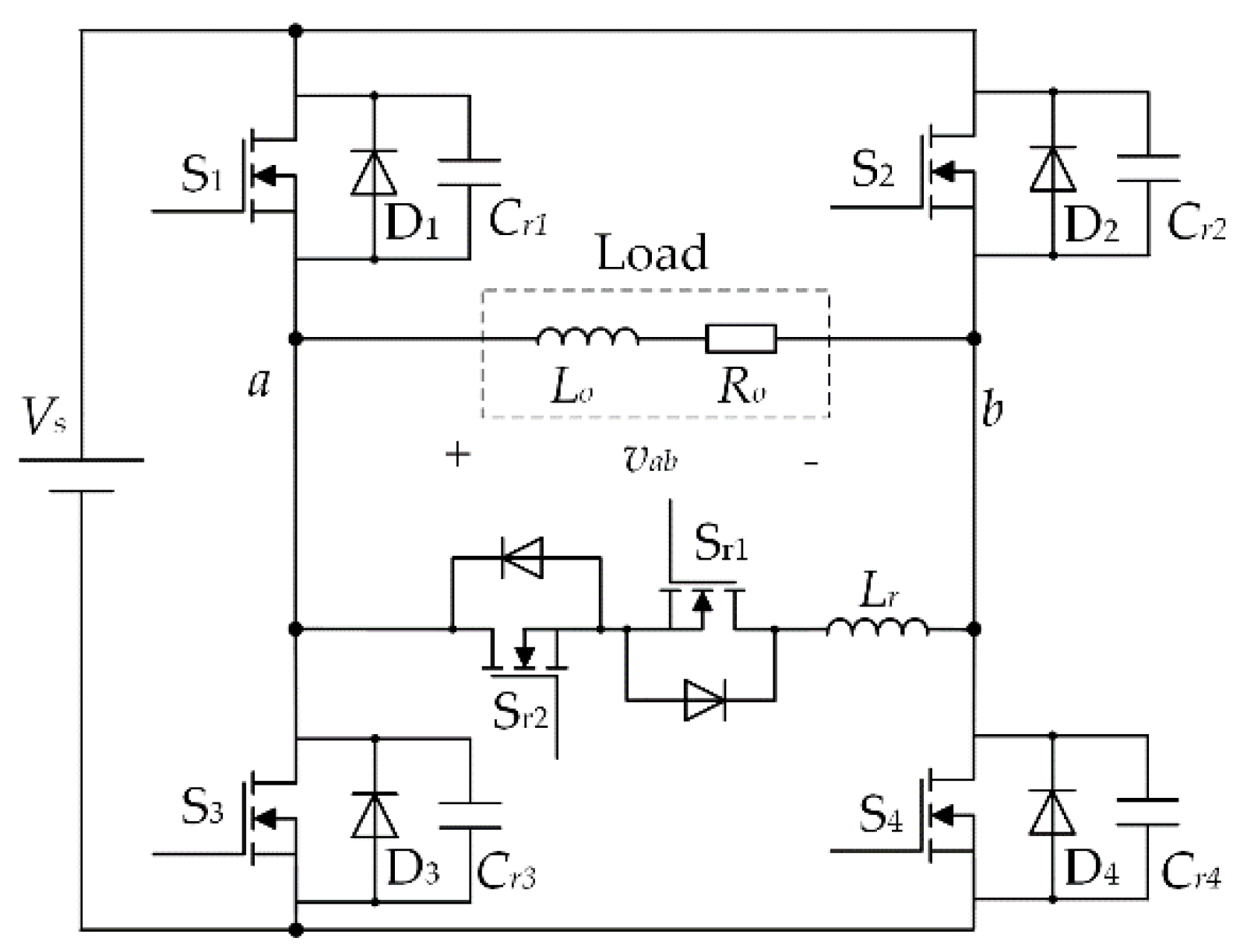
2. Dead-Time Effect of the Auxiliary Resonant Snubber Inverter (ARSI)

2.1. Principle

Figure 1 depicts the single-phase ARSI topology analyzed in this paper, which consists of a standard H-bridge inverter, resonant capacitors and an auxiliary circuit. With a proper operation of the auxiliary switches, Sr1 and Sr2, the zero-voltage-switching (ZVS) condition of the main switches, S1-S4, can be created. Meanwhile, the auxiliary switches can realize zero-current switching (ZCS).
In order to realize soft-switching for the entire load range and maintain a low auxiliary current, the ARSI operates in two modes of heavy load mode (HLM) and light load mode (LLM), as determined by the load condition [22]. In the heavy load condition, the auxiliary circuit is only operated once in each switching period, thus achieving auxiliary ZVS (AZVS) of a set of switches. The other set of switches can achieve natural ZVS (NZVS) without the operation of auxiliary circuit. In the light load condition, the auxiliary circuit is operated twice in each switching period. Therefore, all the switches achieve AZVS.
The operating principle of the ARSI is introduced in [22]. The detailed dead-time effect of LLM and HLM will be analyzed in the case of positive load current as follows. When the load current is negative, the operation is similar.
To analyze the circuit, we assume that
(1)
All components and devices are ideal;
(2)
The gate signals of the MOSFETs are ideal square-wave;
(3)
The output inductor Lo is high enough to be a constant current source.

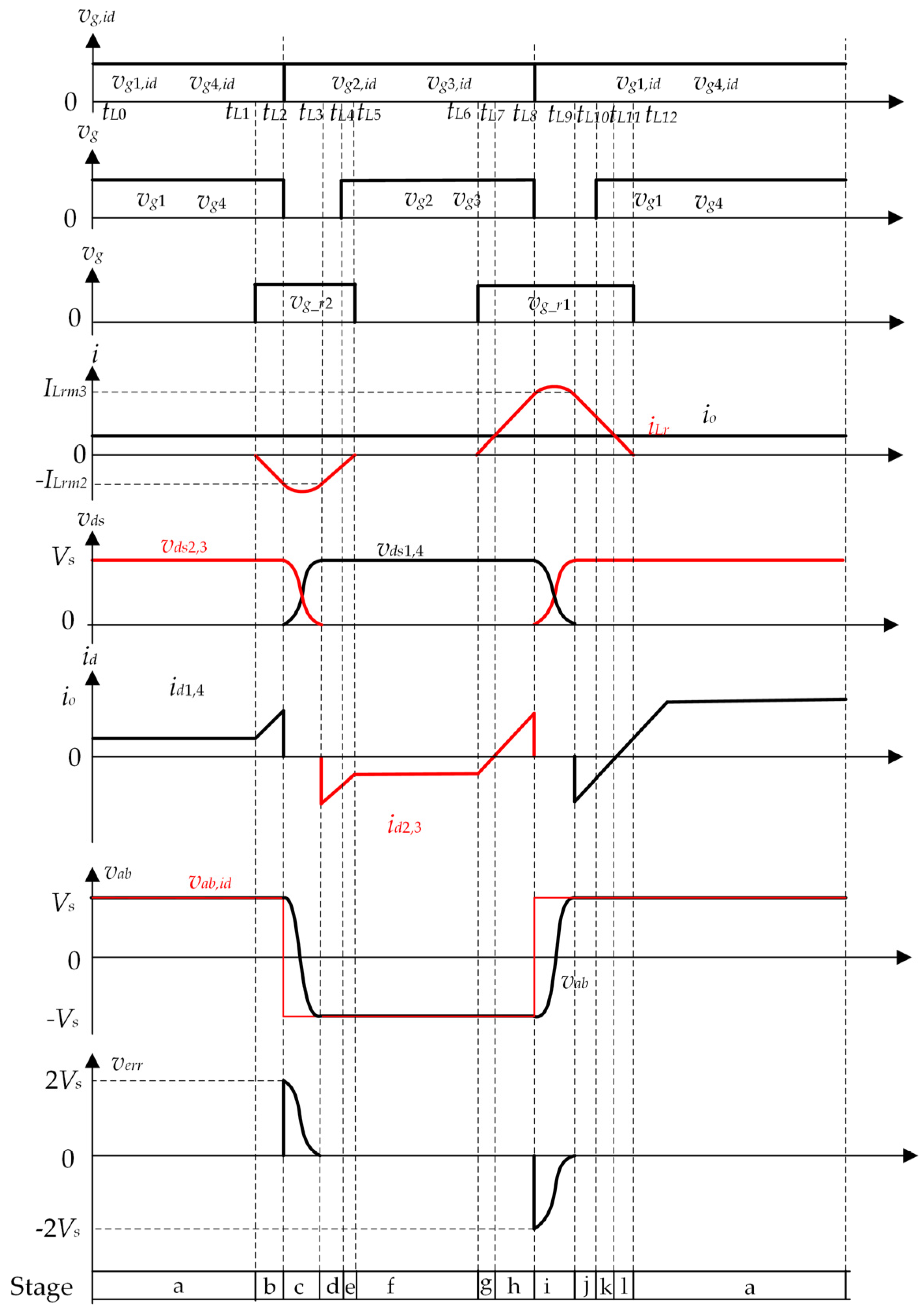
2.1.1. Heavy Load Condition

In the heavy load condition, “AZVS + NZVS,” namely achieving AZVS of a set of switches and NZVS of the other set of switches, is realized. One switching cycle of the operating waveforms are shown in Figure 2, where vds is the drain-source voltage of a MOSFET, id is the drain current of a MOSFET, vg is the actual gate signal with dead-time, vg,id is the ideal gate signal, iLr is the resonant inductor current, vab is the actual pole voltage across the load with dead-time, vab,id is the ideal pole voltage across the load and verr is the voltage error between vab and vab,id.
During the dead-time tH1tH3, the resonant capacitors first resonate with the load inductor. Owing to the positive load current, Cr2 and Cr3 are discharged and Cr1 and Cr4 are charged. After Cr2 and Cr3 are discharged to zero-voltage at tH2, the body diodes D2 and D3 conduct the current and then the voltage is clamped to zero. Thus, S2 and S3 can be turned on at the ZVS condition. Regarding the dead-time tH1tH3, it consists of the resonant stage and diode clamping stage. The dead-time causes the pole voltage error. As for the ARSI, the voltage error only occurs in the resonant stage, which is caused by the finite rise- and fall-times of the voltage.
During the resonant stage tH1tH2, the actual pole voltage can be obtained as follows:
v a b ( t ) = V s i o C r ( t t H 1 )
Conversely, the ideal pole voltage should be as follows:
v a b , i d ( t ) = V s
Thus, the voltage error can be given as follows:
v e r r ( t ) = v a b ( t ) v a b , i d ( t ) = 2 V s i o C r ( t t H 1 )
For Equation (1) vab(t) = −Vs, the resonant time can be obtained:
Δ t H 12 = t H 2 t H 1 = 2 C r V s i o
Regarding the next commutation, Sr1 is turned on at tH4 to charge the resonant inductor, so that the switch current reverses at tH5. Therefore, after S2 and S3 are turned off at tH6, the resonant capacitors can resonate with the resonant inductor, which discharges Cr1 and Cr4 to zero-voltage at tH7. Subsequently, the body diodes D1 and D4 conduct the current. Thus, S1 and S4 can be zero-voltage turned on at tH8. Regarding the dead-time tH6tH8, it also consists of the resonant stage and diode clamping stage. Only the resonant stage tH6tH7 brings about the dead-time effect, which is caused by the finite rise- and fall-times. Some equations can be given as follows during the resonant stage.
v d s 1 ( t ) + v d s 3 ( t ) = V s
i c r 1 ( t ) = C r d v d s 1 ( t ) d t
i c r 3 ( t ) = C r d v d s 3 ( t ) d t
i c r 1 ( t ) + i L r ( t ) = i o + i c r 3 ( t )
v d s 1 ( t ) v d s 3 ( t ) = L r d i L r ( t ) d t
The initial resonant condition is given as follows:
v d s 1 ( t H 6 ) = v d s 4 ( t H 6 ) = V s
v d s 2 ( t H 6 ) = v d s 3 ( t H 6 ) = 0
i L r ( t H 6 ) = I L r m
According to Equations (5)–(12), the inductor current and drain-source voltages of the main MOSFETs can be obtained as follows:
i L r ( t ) = ( I L r m i o ) cos ω A ( t t H 6 ) + V s Z A sin ω A ( t t H 6 ) + i o
v d s 1 ( t ) = v d s 4 ( t ) = 1 2 V s + 1 2 V s cos ω A ( t t H 6 ) 1 2 Z A ( I L r m i o ) sin ω A ( t t H 6 )
v d s 2 ( t ) = v d s 3 ( t ) = 1 2 V s 1 2 V s cos ω A ( t t H 6 ) + 1 2 Z A ( I L r m i o ) sin ω A ( t t H 6 )
where ω A = 1 L r C r , Z A = L r C r , and ILrm is the initial resonant inductor current.
The pole voltage can be obtained as follows:
v a b ( t ) = v d s 3 ( t ) v d s 4 ( t ) = Z A I b o o s t 1 sin ω A ( t t H 6 ) V s cos ω A ( t t H 6 )
where Iboost1 is the switch current at the initial resonant time I b o o s t 1 = I L r m 1 i o .
The ideal pole voltage, on the other hand, should be as follows:
v a b , i d ( t ) = V s
The voltage error during the resonant stage tH6tH7 can be calculated as follows:
v e r r ( t ) = v a b ( t ) v a b , i d ( t ) = Z A I b o o s t 1 sin ω A ( t t H 6 ) V s cos ω A ( t t H 6 ) V s
For Equation (16) vab(t) = Vs, the resonant time can be obtained:
Δ t H 67 = t H 7 t H 6 = 2 ω A arcsin V s V s 2 + Z A 2 I b o o s t 1 2
According to the analysis of dead-time effect in the heavy load condition, the voltage error in a switching cycle can be obtained from Equations (3) and (18):
v e r r = { 2 V s i o C r ( t t H 1 )                t H 1 t t H 2 V s V s cos ω A ( t t H 6 ) + Z A I b o o s t 1 sin ω A ( t t H 6 )    t H 6 t t H 7 0          t H 0 t < t H 1 o r t H 2 < t < t H 6 o r t H 7 < t < t H 10
Thus, the average voltage error in a switching cycle can be calculated as follows:
V e r r = 1 T s t H 0 t H 10 v e r r d t = Δ t H 12 Δ t H 67 T s V s = V s T s ( | 2 C r V s i o | | 2 ω A arcsin V s V s 2 + Z A 2 I b o o s t 1 2 | )
where Ts is the switching period.

2.1.2. Light Load Condition

When the load current is low, the resonant capacitors cannot be discharged to zero-voltage during the dead-time. NZVS of S2 and S3 fails [22]. Therefore, the auxiliary circuit is operated to achieve AZVS of S2 and S3. One switching cycle of the operating waveforms in the LLM is shown in Figure 3.
Before tL2, Sr2 is turned on to charge the resonant inductor Lr, thus increasing the switch current. After S1 and S4 are turned off at tL2, the resonant capacitors resonate with the resonant inductor. Due to the higher switch current, Cr2 and Cr3 can be discharged to zero-voltage. Thus, S2 and S3 can be turned on at the ZVS condition. The voltage error also only occurs in the resonant stage tL2tL3. This resonant stage is similar to the stage tH6tH7 in Figure 2. The same equations can be obtained as Equations (5)–(9). However, the initial resonant conditions are different as follows:
v d s 1 ( t L 2 ) = v d s 4 ( t L 2 ) = 0
v d s 2 ( t L 2 ) = v d s 3 ( t L 2 ) = V s
i L r ( t L 2 ) = I L r m 2
Therefore, the inductor current and drain-source voltages of the main MOSFETs can be obtained as follows according to Equations (5)–(9) and (22)–(24):
v d s 1 ( t ) = v d s 4 ( t ) = 1 2 V s 1 2 V s cos ω A ( t t L 2 ) + 1 2 Z A I b o o s t 2 sin ω A ( t t L 2 )
v d s 2 ( t ) = v d s 3 ( t ) = 1 2 V s + 1 2 V s cos ω A ( t t L 2 ) 1 2 Z A I b o o s t 2 sin ω A ( t t L 2 )
i L r ( t ) = I b o o s t 2 cos ω A ( t t L 2 ) V s Z A sin ω A ( t t L 2 ) + i o
where Iboost2 is the switch current at the initial resonant time I b o o s t 2 = I L r m 2 + i o
Thus, the actual pole voltage can be calculated as follows,
v a b ( t ) = v d s 3 ( t ) v d s 4 ( t ) = V s cos ω A ( t t L 2 ) Z A I b o o s t 2 sin ω A ( t t L 2 )
whereas the ideal pole voltage is:
v a b , i d ( t ) = V s
The voltage error caused by the resonant stage can be calculated as follows:
v e r r ( t ) = v a b ( t ) v a b , i d ( t ) = V s cos ω A ( t t L 2 ) Z A I b o o s t 2 sin ω A ( t t L 2 ) + V s
For Equation (28) vab(t) = −Vs, the resonant time can be obtained:
Δ t L 23 = t L 3 t L 2 = 2 ω A arcsin V s V s 2 + Z A 2 I b o o s t 2 2
Regarding the dead-time tL8tL10, the principle is the same as tH6tH8 in the heavy load condition, which is caused by the rise- and fall-times of the pole voltage. Therefore, the voltage error and the resonant time can be obtained:
v e r r ( t ) = Z A I b o o s t 3 sin ω A ( t t L 8 ) V s cos ω A ( t t L 8 ) V s
Δ t L 89 = t L 9 t L 8 = 2 ω A arcsin V s V s 2 + Z A 2 I b o o s t 3 2
where Iboost3 is the switch current at the initial resonant time I b o o s t 3 = I L r m 3 i o
The voltage error in a switching cycle can be obtained from Equations (30) and (32) in the light load condition:
v e r r = { V s cos ω A ( t t L 2 ) Z A I b o o s t 2 sin ω A ( t t L 2 ) + V s    t L 2 t t L 3 V s V s cos ω A ( t t L 8 ) + Z A I b o o s t 3 sin ω A ( t t L 8 )    t L 8 t t L 9 0            t L 0 t < t L 2 o r t L 3 < t < t L 8 o r t L 9 < t < t L 12
Thus, the average voltage error in a switching cycle can be calculated as follows:
V e r r = 1 T s t L 0 t L 12 v e r r d t = Δ t L 23 Δ t L 89 T s V s = V s T s ( | 2 ω A arcsin V s V s 2 + Z A 2 I b o o s t 2 2 | | 2 ω A arcsin V s V s 2 + Z A 2 I b o o s t 3 2 | )

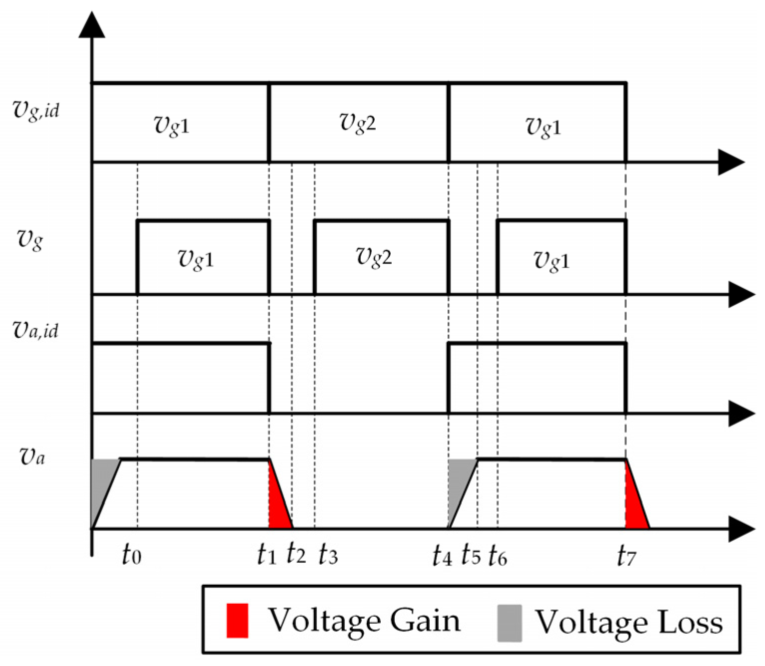
2.2. Compared with the Hard-Switching Inverter

According to the analysis in Section 2.1, the essential principle of ZVS both in the light and heavy load condition is that the resonant capacitors that are parallelly connected to the next turn-on switches are discharged to zero-voltage and then the body diodes conduct the current. Thus, the switches can be turned on with zero-voltage. The dead-time consists of the resonant stage and diode clamping stage. However, the dead-time effect only exists in the resonant stage, which is caused by the finite rise- and fall-times of the voltage. Figure 4 shows the dead-time effect of a single pole, S1 and S3, both in the HLM and LLM where va is the actual pole voltage and va,id is the ideal pole voltage. In order to summarize the dead-time effect both in the HLM and LLM, all the rise- and fall-times are considered to be linearly changed in Figure 4.
As for the hard-switching inverter, the dead-time effect is different from that of the ARSI. To analyze the dead-time effect, the assumption is the same as that of the ARSI. Figure 5 shows the operating stages and key waveforms of the hard-switching inverter with a single pole.
Regarding the dead-time t1t3, the body diode D3 conducts the current after S1 is turned off at t1. The actual pole voltage is clamped to zero, which equals the ideal pole voltage. As for the dead-time t4t6, the current is diverted from S3 to its body diode D3 rather than D1 after the S3 is turned off, because of the positive load current. The pole voltage is clamped to zero, whereas the ideal pole voltage is Vs. Therefore, the voltage loss occurs during the dead-time t4t6. Only after S1 is turned on can the current be diverted to S1. The dead-time causes voltage loss when the output current is positive. However, when the output current is negative, the dead-time leads to voltage gain.
The dead-time effect of the hard-switching inverter is related to the output current polarity, which causes the blanking delay error, whereas the dead-time effect of the ARSI has no relation to the current polarity. Only the rise- and fall-error occurs in the ARSI, rather than the blanking delay error. Essentially, the voltage error caused by the finite commutation time of the voltage also occurs in the hard-switching inverter due to the junction capacitances of the switches. However, compared with blanking delay error, this error can be neglected. Regarding the ARSI, the lower the resonant capacitances, the smaller the voltage error. The dead-time effect can be fully eliminated if the resonant capacitances are zero and the junction capacitances are not considered.

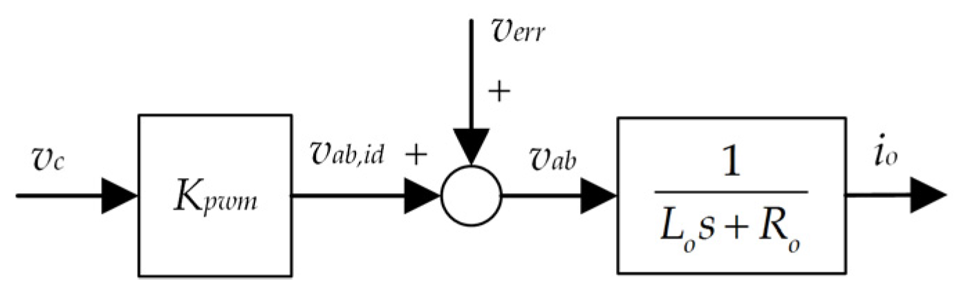
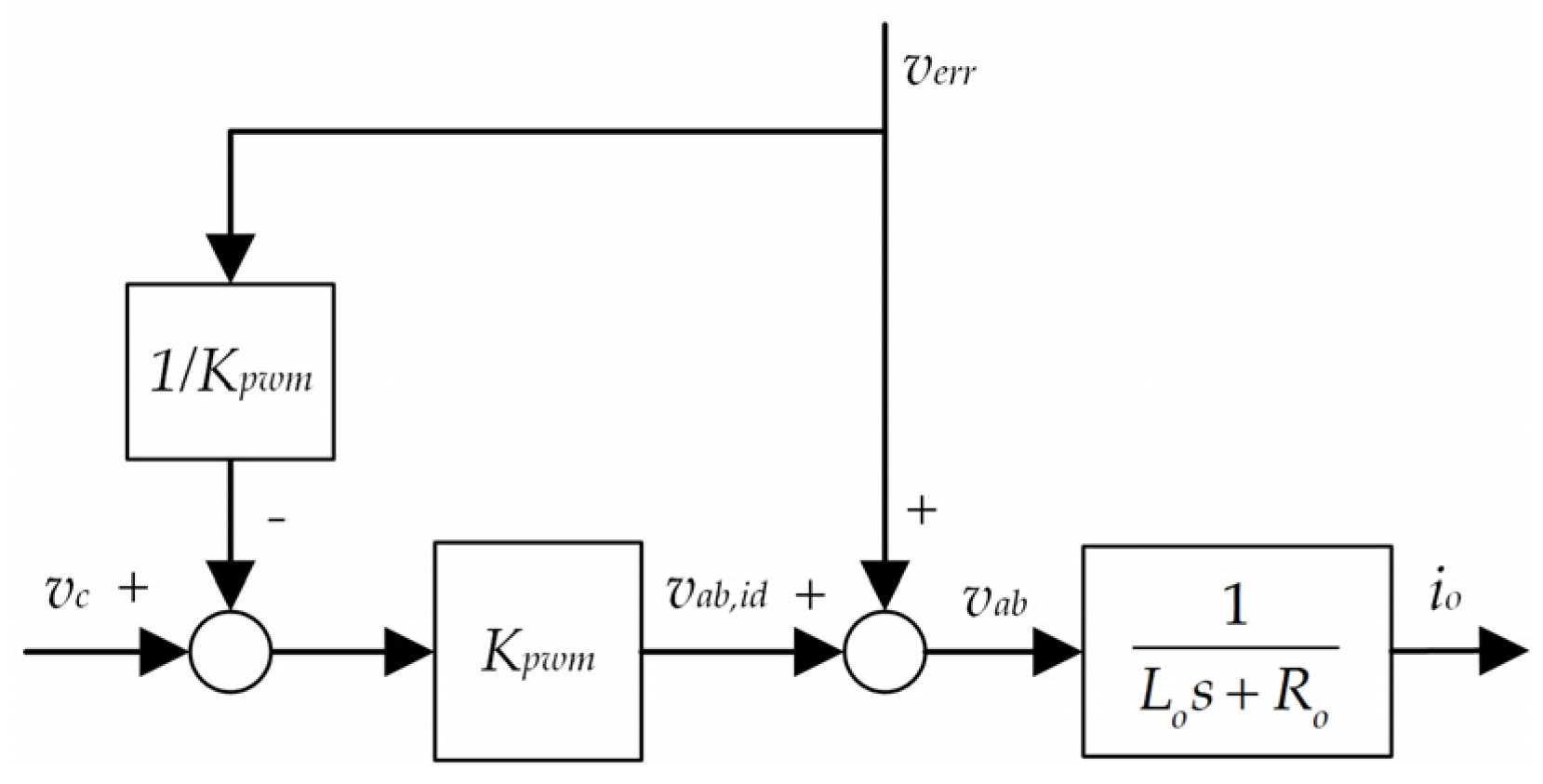
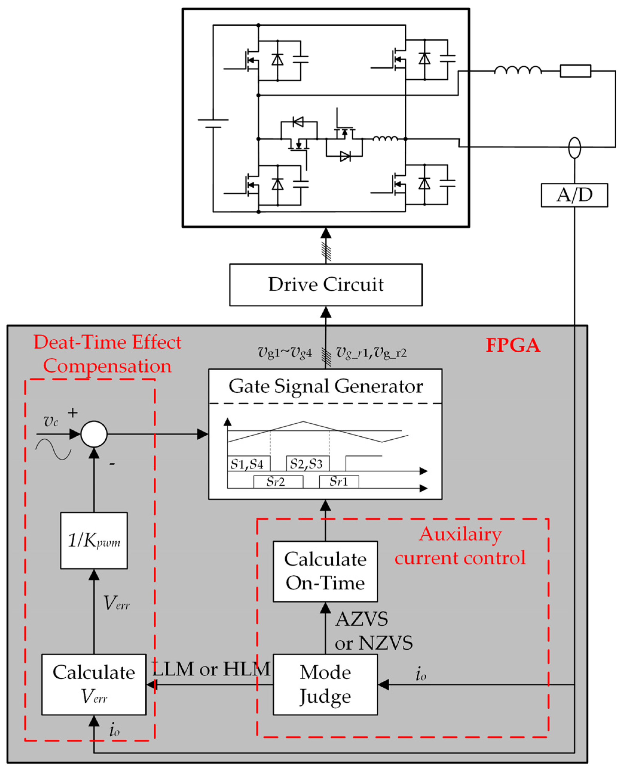
3. Compensation Method

In the HLM, the ZVS realization of the main switches is “AZVS + NZVS.” In the LLM, the ZVS realization is “AZVS + AZVS.” To distinguish the HLM and LLM, the threshold current Ith is used, which is given as follows.
I t h = 2 C r V s t d e a d
When the magnitude of the load current is lower than Ith, the load current cannot discharge the resonant capacitors to zero-voltage. Thus, the ARSI operates in LLM. When the magnitude of the load current is higher than Ith, the HLM is adopted. Table 1 shows the realization type of ZVS from zero load to full load.
The ARSI can reduce the switching loss, whereas the conduction loss is increased due to the auxiliary current. To maintain a low conduction loss, the auxiliary current should be as low as possible. Thus, the initial resonant current Iboost is controlled to be constant from zero load to full load as follows.
I b o o s t 1 = I b o o s t 2 = I b o o s t 3 = I b o o s t
The dead-time effect in the case of positive output current is introduced in Section 2.1. When the output current is negative, the dead-time effect is similar. Therefore, the voltage error caused by the dead-time can be obtained based on Equations (21), (35) and (37):
V e r r = { V s T s ( | 2 C r V s i o | | 2 ω A arcsin V s V s 2 + Z A 2 I b o o s t 2 | ) i o > I t h 0               I t h i o I t h V s T s ( | 2 ω A arcsin V s V s 2 + Z A 2 I b o o s t 2 | | 2 C r V s i o | ) i o < I t h
The voltage error is related to the resonant time. Due to the same Iboost, the voltage error is zero in the LLM. As for the HLM, the voltage error occurs because the resonant time is adaptively related to the output current to achieve NZVS, whereas the commutation time to achieve AZVS is constant.
Due to the dead-time effect, a voltage error occurs between the actual pole voltage and ideal pole voltage. The ARSI can be modeled as a proportional gain Kpwm without consideration of delays. Kpwm is the ratio between the DC voltage and peak value of the carrier in the PWM modulator. The reference voltage vc is amplified Kpwm, thus obtaining the ideal pole voltage vab,id. The actual pole voltage can be obtained by adding the voltage error verr. Figure 6 shows the transfer function of the ARSI.
The output current can be calculated as follows.
i o = 1 L o s + R o v a b , i d + 1 L o s + R o v e r r
where the actual voltage v a b , i d = K p w m v c .
The voltage error caused by the dead-time effect is considered as a disturbance in the ARSI. To compensate the voltage error, the feedforward method can be utilized, which is shown in Figure 7.
After the feedforward compensation is utilized, the output current can be calculated as follows.
i o = 1 L o s + R o [ ( v c v e r r K p w m ) K p w m + v e r r ] = 1 L o s + R o v a b , i d
According to Equations (39) and (40), the dead-time effect can be eliminated by using the proposed compensation method theoretically.

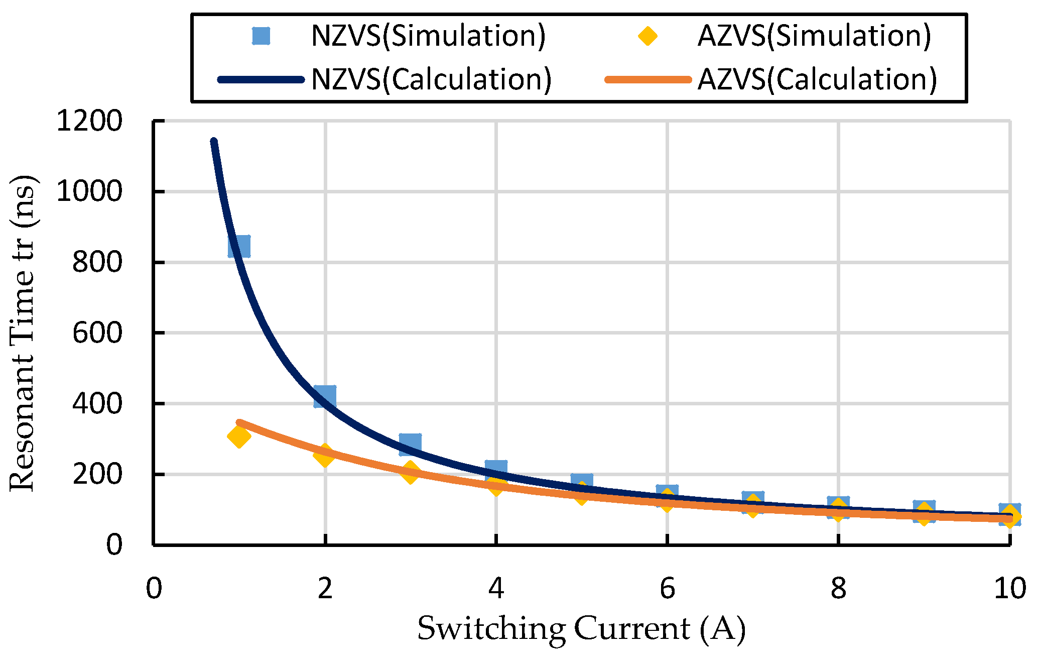
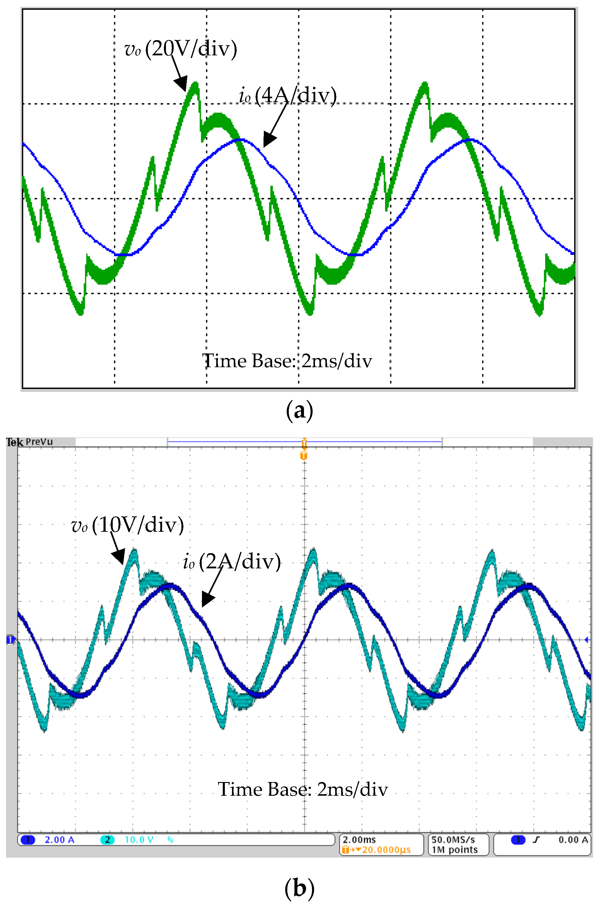
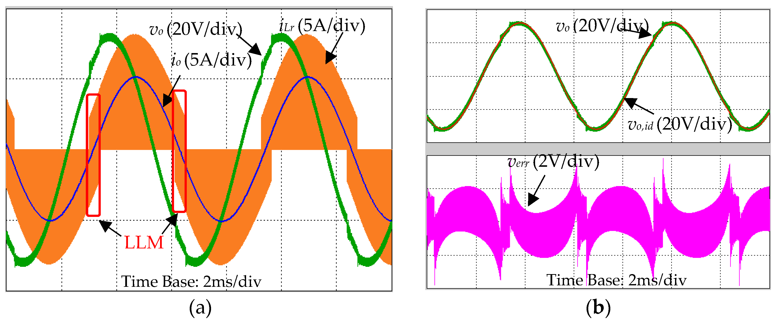
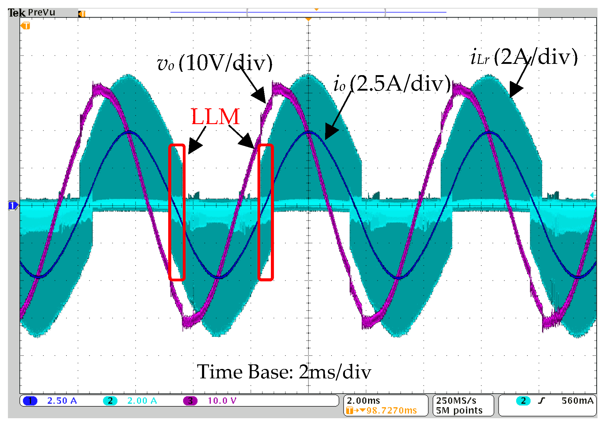
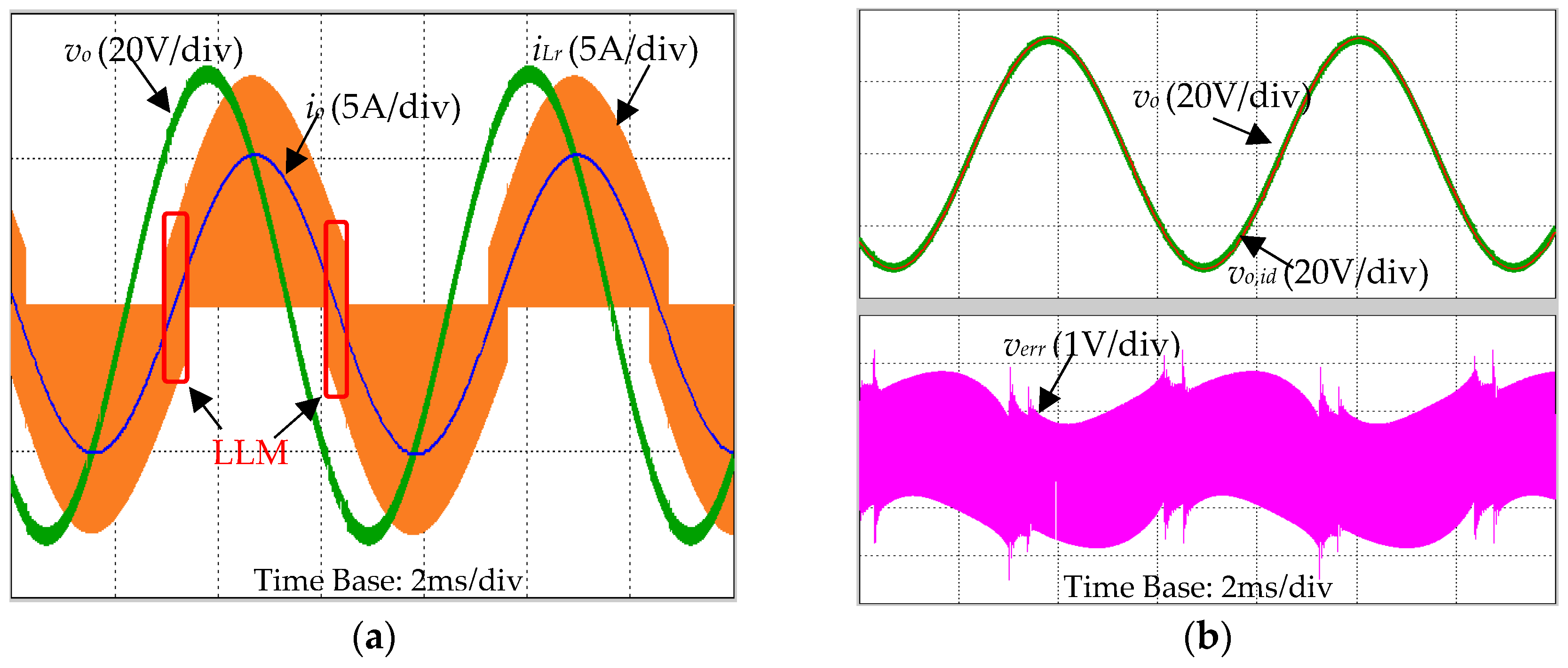
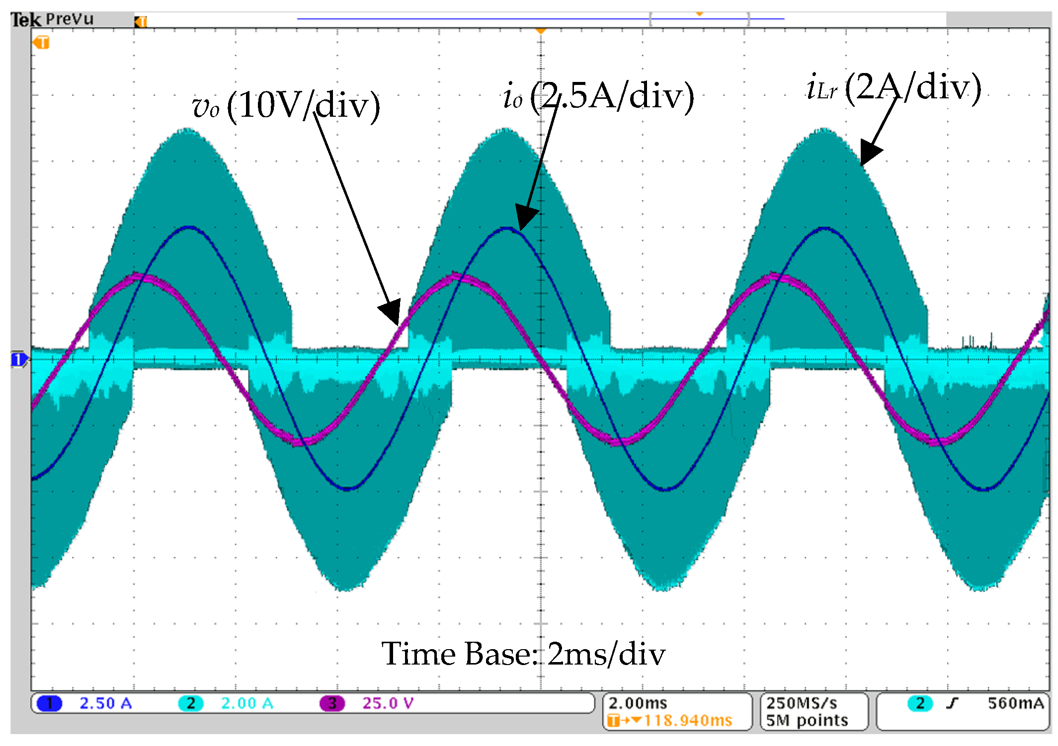
4. Simulation and Experiment

The proposed compensation method was implemented in the Altera Cyclone IV FPGA of a digitally controlled ARSI prototype using the parameters listed in Table 2. Figure 8 shows the photograph of the prototype, which consists of a FPGA (Altera Corporation EP4CE22E22C7N) control board, a switching power supply, a MOSFET driver and a power circuit. In addition, the method is also verified in the simulation using Saber.
Figure 9 shows the open-loop control diagram of the ARSI with proposed dead-time effect compensation. FPGA samples the output current in each switching cycle. Then the mode judgement is completed according to Table 1. The voltage error can be calculated from Equation (38). Therefore, the voltage error can be compensated in the reference voltage. As for the auxiliary current control, the on-time of the auxiliary switches can be calculated after the mode judgement. Finally, the gate signals of the switches can be generated from the compensated reference voltage and the on-time of the auxiliary switches.
The compensation method is based on the model of the voltage error. The more accurate the model, the more precise the compensation result. Figure 10 shows the calculated voltage error vs. output current according to Equation (38). The voltage error only occurs in the HLM. A voltage error about 1.2 V occurs at the threshold current 3A. As the output current increases, the voltage error decreases first before increasing.
Figure 11 shows the resonant time vs. the switching current both in the calculation and simulation, where the switching current of AZVS is Iboost and the switching current of NZVS is io. The resonant time of AZVS is nonlinear related to the switching current. When the switching current is high enough, the resonant time of AZVS is close to that of NZVS. The calculation of the resonant time is in good agreement with the simulation results, which is related to the voltage error.
Figure 12 shows the output voltage and current of the hard-switching inverter when the modulation index is 0.4 in an open-loop configuration. To measure the output voltage vo, a filter is added to attenuate the carrier harmonics of the pole voltage vab. A serious distortion occurs both in the output current and voltage due to the long dead-time of 0.5 μs.
Figure 13 and Figure 14 show the simulation and experimental results of ARSI without dead-time compensation, respectively, when the modulation index is 0.4 in an open-loop configuration. The auxiliary circuit is operated twice with bidirectional current in a switching cycle in the LLM. An obvious distortion occurs in the output voltage at the mode switching point. However, the distortion of the output current and voltage is less than that of the hard-switching inverter in Figure 12, owing to the absence of blanking delay error in the ARSI. Figure 13b shows the voltage error between the actual output voltage and ideal output voltage. The simulation results are in good agreement with the calculation results in Figure 10 without consideration of the ripple. The maximum voltage error is about 2 V and occurs at the mode switching point.
Figure 15 and Figure 16 show the simulation and experimental results, respectively, when the proposed compensation method is used in the ARSI. The output voltage distortion is reduced in Figure 15a and Figure 16 without increasing the auxiliary current iLr. Figure 15b demonstrates that the voltage error is reduced.
Figure 17 shows the magnitudes of the 2nd–10th harmonic components with respect to the fundamental component in the output voltage and current. The power analysis module DPO4PWR is used to analyze the total harmonic distortions (THDs) of the current and voltage. Figure 17a demonstrates that THD of the output voltage with the compensation method is 3.48% which is less than 6.29% than without dead-time effect compensation. The magnitudes of the 2nd–10th harmonics are reduced, except for the 8th harmonic. Figure 17b indicates that THD of the output current is reduced from 1.57% to 0.712% by using the proposed compensation method.
Figure 18 shows the experimental voltage and current THDs under different load conditions. As the modulation index increases, the THDs of the output voltage and current both decrease. Through using the dead-time compensation strategy, the THDs of the output voltage and current are clearly reduced.

5. Conclusions

In this paper, the dead-time effect of a typical zero-voltage-switching (ZVT) inverter—the auxiliary resonant snubber inverter (ARSI)—is analyzed. The ARSI can fully eliminate the blanking delay error which is the main drawback of the hard-switching inverter. Only the rise- and fall-error caused by the resonant capacitors occurs in the ARSI, which is not considered in the hard-switching inverter. In the simulation and experiment, the quality of the output in the ARSI is significantly better than that in the hard-switching inverter, even if the dead-time compensation strategy is not used.
Furthermore, a feed-forward compensation method based on the voltage error estimation is proposed to compensate the rise- and fall-error of dead-time effect. Both the simulation and experimental results show that the compensation strategy can effectively reduce the THDs of the outputs.

Acknowledgments

This work was supported by the State Key Program of National Natural Science of China under Grant 51537002 and the National Natural Science Foundation of China under Grant 51607044.

Author Contributions

Hailin Zhang conceived the proposed method and wrote the paper; Baoquan Kou provided technical guidance and good advice for the manuscript; Lu Zhang and He Zhang performed the experiments and reviewed the manuscript.

Conflicts of Interest

The authors declare no conflict of interest.

References

  1. Leggate, D.; Kerkman, R. Pulse-based dead-time compensator for PWM voltage inverters. IEEE Trans. Ind. Electron. 1997, 38, 191–197. [Google Scholar] [CrossRef]
  2. Zhang, Z.; Xu, L. Dead-time compensation of inverters considering snubber and parasitic capacitance. IEEE Trans. Power Electron. 2014, 29, 3179–3187. [Google Scholar] [CrossRef]
  3. Mannen, T.; Fujita, H. Dead-time compensation method based on current ripple estimation. IEEE Trans. Power Electron. 2015, 30, 4016–4024. [Google Scholar] [CrossRef]
  4. Pellegrino, G.; Bojoi, R.I.; Guglielmi, P.; Cupertino, F. Accurate inverter error compensation and related self-commissioning scheme in sensorless induction motor drives. IEEE Trans. Ind. Appl. 2010, 46, 1970–1978. [Google Scholar] [CrossRef]
  5. Berkhout, M. A class D output stage with zero dead time. In Proceedings of the International Solid-State Circuits Conference, San Francisco, CA, USA, 13 February 2003; pp. 134–135.
  6. Lin, Y.K.; Lai, Y.S. Dead-time elimination of PWM-controlled inverter/converter without separate power sources for current polarity detection circuit. IEEE Trans. Ind. Electron. 2009, 56, 2121–2127. [Google Scholar]
  7. Chen, L.; Peng, F.Z. Dead-time elimination for voltage source inverters. IEEE Trans. Power Electron. 2008, 23, 574–580. [Google Scholar] [CrossRef]
  8. Ben-Brahim, L. On the compensation of dead time and zero-current crossing for a PWM-inverter-controlled AC servo drive. IEEE Trans. Ind. Electron. 2004, 51, 1113–1117. [Google Scholar] [CrossRef]
  9. Summers, T.J.; Betz, R.E. Dead-time issues in predictive current control. IEEE Trans. Ind. Appl. 2004, 40, 835–844. [Google Scholar] [CrossRef]
  10. Zhang, L.; Gu, B.; Dominic, J.; Chen, B.; Zheng, C.; Lai, J. A dead-time compensation method for parabolic current control with improved current tracking and enhanced stability range. IEEE Trans. Power Electron. 2015, 30, 3892–3902. [Google Scholar] [CrossRef]
  11. Guo, Z.; Kurokawa, F. A new hybrid current control scheme for deadtime compensation of inverters with LC filter. In Proceedings of the 13th European Conference on Power Power Electronics and Applications, Barcelona, Spain, 8–10 September 2009; pp. 1–10.
  12. Nielsen, K. Linearity and efficiency performance of switching audio power amplifier output stages-a fundamental analysis. In Proceedings of the 105th Audio Engineering Society Convention, San Francisco, CA, USA, 26–29 September 1998.
  13. McMurray, W. Resonant snubbers with auxiliary switches. IEEE Trans. Ind. Appl. 1993, 29, 355–362. [Google Scholar] [CrossRef]
  14. DeDonker, R.W.; Lyons, J.P. The auxiliary resonant commutated pole converter. In Proceedings of the Industry Applications Society Annual Meeting, Seattle, WA, USA, 7–12 October 1990; pp. 1228–1235.
  15. Lai, J.S. Resonant snubber-based soft-switching inverters for electric propulsion drives. IEEE Trans. Ind. Electron. 1997, 44, 71–80. [Google Scholar]
  16. Lai, J.S.; Young, R.W.; Ott, G.W.; McKeever, J.W.; Peng, F.Z. A delta-configured auxiliary resonant snubber inverter. IEEE Trans. Ind. Appl. 1996, 32, 518–525. [Google Scholar]
  17. Yuan, X.; Barbi, I. Analysis, designing, and experimentation of a transformer-assisted PWM zero-voltage switching pole inverter. IEEE Trans. Power Electron. 2000, 15, 950–950. [Google Scholar]
  18. Russi, J.L.; da Silva Martins, M.L.; Hey, H.L. Coupled-filter-inductor soft-switching techniques: Principles and topologies. IEEE Trans. Ind. Electron. 2008, 55, 3361–3373. [Google Scholar] [CrossRef]
  19. Yu, W.; Lai, J.; Park, S. An improved zero-voltage switching inverter using two coupled magnetics in one resonant pole. IEEE Trans. Power Electron. 2010, 25, 952–961. [Google Scholar]
  20. Beltrame, R.C.; Rakoski Zientarski, J.R.; da Silva Martins, M.L.; Pinheiro, J.R.; Hey, H.L. Simplified zero-voltage-rransition circuits applied to bidirectional poles: Concept and synthesis methodology. IEEE Trans. Power Electron. 2011, 26, 1765–1776. [Google Scholar] [CrossRef]
  21. Russi, J.L.; da Silva Martins, M.L.; Schuch, L.; Pinheiro, J.R.; Hey, H.L. Synthesis methodology for multipole ZVT converters. IEEE Trans. Ind. Electron. 2007, 54, 1783–1795. [Google Scholar] [CrossRef]
  22. Kou, B.; Zhang, H.; Jin, Y.; Zhang, H. An Improved Control Scheme for Single-Phase Auxiliary Resonant Snubber Inverter. In Proceedings of the IEEE 8th International Power Electronics and Motion Control Conference, Hefei, China, 22–26 May 2016; pp. 1259–1263.
Figure 1. Circuit of auxiliary resonant snubber inverter.
Applsci 06 00344 g001
Figure 2. Key waveforms of the the auxiliary resonant snubber inverter (ARSI) in the heavy load condition.
Applsci 06 00344 g002
Figure 3. Key waveforms of the ARSI in the light load condition.
Applsci 06 00344 g003
Figure 4. Dead-time effect of the ARSI.
Applsci 06 00344 g004
Figure 5. Dead-time effect of hard-switching inverter with single pole (a) the operating stages when io > 0; (b) the key waveforms when io > 0; (c) the key waveforms when io < 0.
Applsci 06 00344 g005
Figure 6. Transfer function of the ARSI.
Applsci 06 00344 g006
Figure 7. Transfer function of the ARSI with feedforward compensation.
Applsci 06 00344 g007
Figure 8. Photograph of the prototype.
Applsci 06 00344 g008
Figure 9. Open-loop control diagram of the ARSI with proposed dead-time effect compensation.
Applsci 06 00344 g009
Figure 10. Average voltage error vs. output current in the calculation.
Applsci 06 00344 g010
Figure 11. Resonant time vs. the switching current both in the calculation and simulation.
Applsci 06 00344 g011
Figure 12. Output voltage and current of the hard-switching inverter when the modulation index is 0.4 in an open-loop configuration. (a) simulation results; (b) experimental results.
Applsci 06 00344 g012
Figure 13. Simulation waveforms of ARSI without dead-time compensation when the modulation index is 0.4 in an open-loop configuration. (a) simulation results; (b) voltage error.
Applsci 06 00344 g013
Figure 14. Experimental waveforms of ARSI without dead-time compensation when the modulation index is 0.4 in an open-loop configuration.
Applsci 06 00344 g014
Figure 15. Simulation waveforms of ARSI with dead-time compensation when the modulation index is 0.4 in an open-loop configuration. (a) simulation results; (b) voltage error.
Applsci 06 00344 g015
Figure 16. Experimental waveforms of ARSI with dead-time compensation when the modulation index is 0.4 in an open-loop configuration.
Applsci 06 00344 g016
Figure 17. Magnitudes of the 2nd–10th harmonic components in respect to the fundamental component (a) output voltage; (b) output current.
Applsci 06 00344 g017
Figure 18. Experimental voltage and current THDs under different load condition (a) voltage THD; (b) current THD.
Applsci 06 00344 g018
Table 1. Realization type of ZVS from zero load to full load.
Typeio < –IthIthioIthio > Ith
S2 and S3AZVS (Sr2)AZVS (Sr2)NZVS
S1 and S4NZVSAZVS (Sr1)AZVS (Sr1)
Load ConditionHeavy LoadLight LoadHeavy Load
Table 2. Parameters of the circuit.
ParameterValue
DC voltage Vs80 V
Switching frequency fs200 kHz
Dead-time tdead0.5 μs
Load3.7 Ω, 4.87 mH
Resonant inductor Lr4.4 μH
Resonant capacitor Cr4.7 nF
Threshold current Ith3 A
Iboost4 A

