2. Dynamics of Free Carriers in Nanomaterials
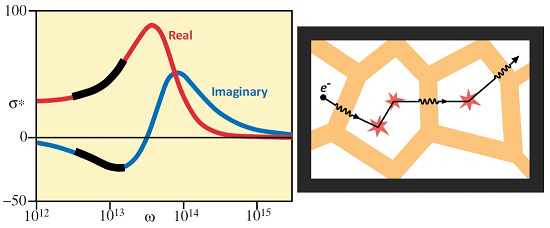
Before proceeding with discussion, we will show a difference between the Drude relaxation and the Lorentz resonance in terms of the complex (optical) conductivity, σ*(ω) = σ
R(ω) +
iσ
I(ω) [
3]. Note that the local electric field is taken to vary in time as exp(−
iω
t). Solid and dotted lines, (a) and (b), show the real and imaginary parts of conductivity, σ
R(ω) and σ
I(ω), respectively, for the Drude relaxation, and lines (c) and (d) are for the Lorentz resonance. A frequency-independent real part of conductivity in curve (a) gives the dc conductivity. We hence expect that the low-frequency real part of conductivity (energy loss) corresponds to the dc conductivity (dc loss), when the transport is dominated by the Drude law. As already stated, a Lorentz-type behavior dominates THz conductivity in most of nanomaterials. We, therefore, discuss why do free carriers behave as a Lorentz-like resonance, since free carriers should follow the Drude law in usual understanding.
A few models have been proposed for the origin of the Lorentz-type resonance behavior [
1]. We know that a quantum mechanical electronic (optical) transition between states is well described by the Lorentz resonance. In the following, we state briefly the models so far proposed:
(1) When a motion of free carriers involves a restoring force,
i.e., the restoring force is added in the Drude equation, the equation of motion is described by a damped harmonic oscillator, which should leads to the Lorentz oscillator [
3]. A surface depletion or accumulation field can be a source of the restoring force. This is called the plasmon model and was applied to semiconductor nanoparticles [
1,
20].
(2) By assuming only one backscattering of free carriers, complex conductivity shows the Lorentz-type behavior, which is called the generalized Drude model or the Drude-Smith (DS) model [
21]. As the DS model has been most widely used to explain the non-Drude behavior [
1], we summarize here the DS approach. A complex conductivity given by Smith [
21] is given as:
where σ(0) is the Boltzmann dc conductivity given by e
2nfτ/
m*,
nf is the density of free carrier,
m* the effective mass, τ the scattering time, and ω the angular frequency of external excitation, assumed to be exp(−
iω
t). The coefficient
cn represents the fraction of the carrier’s original velocity that is retained after the
nth scattering. Note that
n = 0 produces just the Drude law. When we take only one scattering (
n = 1) and −1.0 ≤
c1 < 0 (backscattering), free carrier behavior dramatically changes from the Drude relaxation to the Lorentz-type resonance (see
Figure 1). A large issue in the DS model is that there is no proper physical basis, while good fitting to the experimental results is obtained. Note also that the DS model should basically be applied to homogeneous media.
Figure 1.
Optical conductivity in the Drude relaxation ((a) and (b)) and in the Lorentz resonance ((c) and (d)).
Figure 1.
Optical conductivity in the Drude relaxation ((a) and (b)) and in the Lorentz resonance ((c) and (d)).
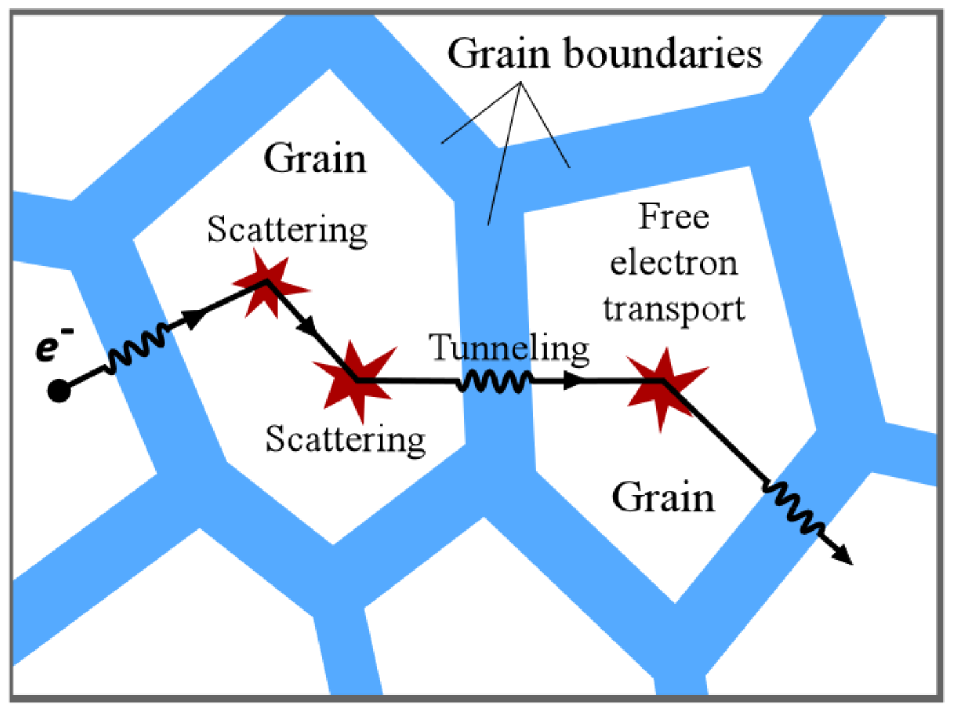
(3) When we discuss the electronic transport in inhomogeneous media, such as nanoparticles with grain boundaries, charge transfer can occur from one constituent to another. Thus, the role of interfaces (grain boundaries) may be important. A schematic view for such carrier transport is shown in
Figure 2.
Figure 2.
Schematic view of carrier transport within grains (intragrain) and through grain boundaries (intergrain) in nanomaterials
Figure 2.
Schematic view of carrier transport within grains (intragrain) and through grain boundaries (intergrain) in nanomaterials
We call this a series sequence of the free (intragrain) and tunneling (intergrain; grain boundary) carrier (SSFTC) transport model [
2,
22]. Let us review the SSFTC formalism. As stated already, the frequency dependence of complex conductivity for free carrier is given by the Drude law (
n = 0 in Equation (1)) as:
Note that τ in this equation should be viewed as an effective relaxation time that accounts for various scattering processes within the grain, so-called intragrain scattering processes. For the tunneling transport, the so-called Dyre expression, based on an effective medium approach, which should be equivalent to a parallel capacitor-resistor random connection, is adopted [
23]. The tunneling conductivity is given as:
where σ
t(0) is the dc tunneling conductivity and is given by
nt(e
rt)
2/2
kTτ
t. Here,
nt is the density of tunneling carrier,
rt the tunneling length (distance between grains), and τ
t the tunneling time. The effective (overall) complex conductivity, in a simple one-dimensional approximation [
23,
24,
25], is given as [
2,
22]:
where
f is the spectral weight of intragrain transport.
As will be discussed in
Section 3, σ
eff*(ω) shows Lorentz-type resonance, as was found in the DS model. The negative imaginary conductivity, curve (d) in the Lorentz resonance, originates from capacitive nature of electronic charge. It should be emphasized here that a series sequence of the Drude and the Debye-type relaxations produces Lorentz-type resonance.
(4) An effective medium theory (EMT) [
26] is expected also to apply to THz conductivity in inhomogeneous media [
1]. The EMT should be employed to model the composite materials, in particular when charge transfer between composites has not occurred, e.g., relatively small fraction of metallic (or high conductive) component in insulators. The Lorentz-like resonance is predicted from the EMT calculation [
1]. A loss-peak frequency (see curve (c) in
Figure 1) highly depends on the plasma frequency,
i.e., depends on free carrier density, and, hence, significant loss-peak shift should be observed in such media, similar to the plasmon case. In fact, in common with nanomaterials of metals and semiconductors, the loss peak may lie in THz frequency range (no big shift in a loss peak).
We thus conclude that the SSFTC model is the best model to explain the electronic transport in nanomaterials. Typical examples are shown in the following section.
3. Typical Examples of THz Conductivity in Nanomaterials
For the purposes of this focused review, we will consider and discuss only a few selected examples of the THz conductivity, such as popular nano- semiconductors, oxides, and metals, rather than a comprehensive and extensive review. An extensive review of a large collection of materials is beyond the scope of this focused review. Note that the following experimental data are all provided by pulsed sources based on terahertz time-domain spectroscopy (THz-TDS) and measured at room temperature. There are a number of excellent reviews on this topics [
1,
27] and, therefore, we do not discuss THz techniques in this article.
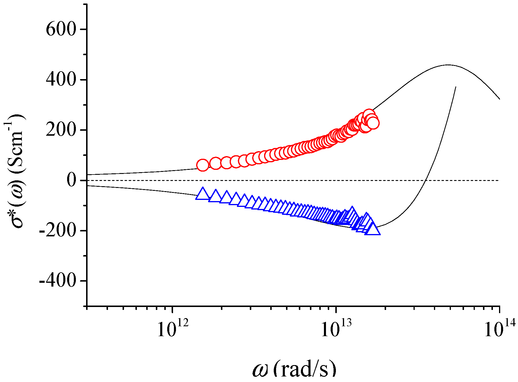
Open circles and triangles in
Figure 3 show the experimental results of real and imaginary parts of conductivity, respectively, in nanocrystalline Si films (average grain size is 15–25 nm) [
8]. To extract the complex conductivity we use the relationship between the dielectric permittivity and conductivity given as:
where ε*(ω) + ε
∞ = ε
R(ω) +
iε
I(ω), ε
0 is the absolute permittivity, ε
R(ω) and ε
I(ω) are the real and imaginary part of dielectric constants, respectively, and ε
∞ is the background dielectric constant. Note again that a time dependence of the form exp(−
iω
t) is used here. Optical pumping spectroscopy has been used for producing enough free carriers (electrons) at room temperature, and, hence, we do not need ε
∞ for calculation as a physical parameter [
1]. The negative value of the imaginary part of conductivity is obtained.
Figure 3.
Complex conductivity in nanocrystalline Si films. Open circles and triangles are experimental results of the real and imaginary parts of conductivity, respectively; data extracted from [
8]. Solid lines are conductivity predicted from the SSFTC model.
Figure 3.
Complex conductivity in nanocrystalline Si films. Open circles and triangles are experimental results of the real and imaginary parts of conductivity, respectively; data extracted from [
8]. Solid lines are conductivity predicted from the SSFTC model.
Solid lines in
Figure 3 show the best fit of the SSFTC model to the experimental data. Adjusted physical parameters are all reasonable and are listed in
Table 1. We now recognize that the SSFTC model predicts a similar behavior of the Lorentz resonance as shown in
Figure 1 (curves (c) and (d)). It is important to emphasize that experimental data are only available within a certain narrow frequency range. In the present case, a peak is predicted by the model outside the experimental frequency window. Fitting within the data range leads to a peak outside the data range, but there is no way of validating this prediction without extending the experimental data range to cover the peak. However, as will be shown for nanogold particles (
Figure 7), a peak is indeed found in the observed frequency range. We, therefore, discuss a detailed comparison between the Lorentz resonance and the SSFTC prediction in the final part of this section.
Table 1.
Physical parameters used for calculation in the series sequence of the free and tunneling carrier (SSFCT) transport model. σdc is the measured dc conductivity.
Table 1.
Physical parameters used for calculation in the series sequence of the free and tunneling carrier (SSFCT) transport model. σdc is the measured dc conductivity.
| Quantity | Si | Ge2Sb2Te5 | ZnO | SnO2 | Au | Cryst-ZnO |
|---|
| f | 0.83 | 0.996 | 0.94 | 0.97 | 0.999 | 1 |
| m* | 0.3 | 0.3 | 0.3 | 0.3 | 1 | 0.24 |
| n (cm−3) | 5.3 × 10¹⁸ | 1.5 × 10²⁰ | 7.0 × 10¹⁹ | 1.0 × 10²⁰ | 1.0 × 10²² | 4.5 × 10¹⁷ |
| τ (s) | 2.0 × 10⁻¹⁴ | 2.4 × 10⁻¹⁴ | 4.0 × 10⁻¹⁴ | 5.0 × 10⁻¹⁴ | 3.0 × 10⁻¹⁴ | 2.7 × 10⁻¹⁴ |
| nt (cm−3) | 2.0 × 10¹⁹ | 2.0 × 10¹⁹ | 1.6 × 10¹⁸ | 1.6 × 10¹⁸ | 1.5 × 10²¹ | - |
| τt (s) | 4.0 × 10⁻¹³ | 2.0 × 10⁻¹¹ | 2.0 × 10⁻¹⁴ | 9.0 × 10⁻¹³ | 3.0 × 10⁻¹² | - |
| ε∞ | - | 320 | 14 | 15 | 1 | - |
| σeff(0) (S cm−1) | 28.0 | 15.4 | 4.0 | 11.4 | 55,000 | 142 |
| σdc (S cm−1) | 1–10 | 20 | 4 | 0.6 | - | 46 |
Open circles and triangles in
Figure 4 show the real and imaginary parts of conductivity in the crystalline phase of Ge
2Sb
2Te
5 (from the Kadlec group at the Academy of Sciences of the Czech Republic in Pargue), which is the most useful phase-change material, developed for digital versatile disk (DVD) [
28]. As the crystalline phase of phase-change materials is a degenerate semiconductor ( witha high density of free carriers) and, hence, the optical-pumping (photocarrier) technique, as in nanocrystalline Si (see
Figure 3) is not required. In this case, background conductivity (imaginary), σ
∞ = ωε
0ε
∞, is taken into account [
1,
2]. Solid lines show the real and imaginary parts of conductivity predicted by the SSFTC model, and the physical parameters from the fitting are listed in
Table 1. Note that features obtained here are very similar to those obtained for other phase-change materials [
14].
Figure 4.
Complex conductivity in crystalline phase of Ge2Sb2Te5 films. Open circles and triangles are experimental results of the real and imaginary parts of conductivity, respectively. Solid lines are conductivity predicted from the SSFTC model.
Figure 4.
Complex conductivity in crystalline phase of Ge2Sb2Te5 films. Open circles and triangles are experimental results of the real and imaginary parts of conductivity, respectively. Solid lines are conductivity predicted from the SSFTC model.
Let us examine the THz conductivity in so-called oxide metals and semiconductors. ZnO and SnO
2, for example, show both metallic and semiconducting natures [
17,
29]. Open symbols in
Figure 5 and
Figure 6 show the complex conductivity in nanostructured ZnO [
17] and SnO
2 [
29] films, respectively.
Fitting of the SSFTC model to the experimental data shown by solid lines produces reasonable physical parameters and these are listed in
Table 1. The both nanostructured oxides discussed here have enough free carriers and hence the optical pumping technique is not employed. Note that the EMT or hopping transport model has been applied to interpret the THz conductivity in Sb-doped SnO
2 [
29]. However, as already stated, the EMT or hopping transport mechanism does not work properly, when nanoparticles are closely packed. The measured σ
dc value (0.5–10 S·cm
−1) [
29] is closed to the effective conductivity deduced from the SSFTC model (see
Table 1).
Figure 5.
Complex conductivity in nanostructured ZnO films. Open circles and triangles, respectively, are the experimental data extracted from [
17]. Solid lines are conductivity predicted from the SSFTC model.
Figure 5.
Complex conductivity in nanostructured ZnO films. Open circles and triangles, respectively, are the experimental data extracted from [
17]. Solid lines are conductivity predicted from the SSFTC model.
Figure 6.
Complex conductivity in nanostructured Sb-doped SnO
2 ((βC
500P-5%). Open circles and triangles are the experimental data extracted from [
29]. Solid lines are predicted conductivity from the SSFTC model.
Figure 6.
Complex conductivity in nanostructured Sb-doped SnO
2 ((βC
500P-5%). Open circles and triangles are the experimental data extracted from [
29]. Solid lines are predicted conductivity from the SSFTC model.
Let us examine the THz conductivity in nanostructured gold films. Open circles and triangles in
Figure 7 show one of examples of the real and imaginary parts of conductivity in nanogold films [
30]. Solid lines are predicted conductivity in the SSFTC model. As the imaginary part of conductivity shows the positive signature (curve (b) in
Figure 1), it seems to be the Drude-type behavior. Fitting to the experimental data shows, however, that grain boundaries dominate the transport and hence the SSFTC model is working well in gold films as well. In fact, the dc conductivity of nanogold films [
4] is very much smaller than that of conventional gold.
Figure 7.
Complex conductivity in nanostructured Au films. Open circles and triangles are the experimental data extracted from [
30]. Solid lines are the conductivity predicted by the SSFTC model.
Figure 7.
Complex conductivity in nanostructured Au films. Open circles and triangles are the experimental data extracted from [
30]. Solid lines are the conductivity predicted by the SSFTC model.
Next, we will show what is observed in a single crystalline material. An example is shown for ZnO epitaxial films in
Figure 8. Open circles and triangles show the real and imaginary parts of conductivity [
31]. Solid lines show the predictions from the Drude law and physical parameters are listed in
Table 1.
Figure 8.
Complex conductivity in single crystalline epitaxial ZnO films. Open circles and triangles are the experimental data extracted from [
31]. Solid lines are the conductivity predicted from the SSFTC model.
Figure 8.
Complex conductivity in single crystalline epitaxial ZnO films. Open circles and triangles are the experimental data extracted from [
31]. Solid lines are the conductivity predicted from the SSFTC model.
A good fit of the Drude law to the experimental results in epitaxial GaN has been also reported [
32]. As already stated, the Drude-Smith model [
21], in principle, should be applied to single crystalline materials since the disorder effect is not important in the DS model; it is simply a generalization of the Drude formula. No such non-Drude behavior, which fits to the DS model, is reported.
It was stated that the SSFTC mechanism produces the Lorentz-type resonance, as shown in
Figure 3. In the Lorentz resonance, however, conductivity at a low frequency should be zero. Therefore, the SSFTC model produces a similar trend to the Lorentz resonance. As shown in
Figure 9, when we change physical parameters, e.g., a decrease of
f in Equation (4), in which the tunneling contribution becomes large, the resonant conductivity predicted by the SSFTC model (solid lines) becomes very close to that using the Lorentz resonance (dashed lines), described as [
1,
3]:
here,
N is the number of Lorentz oscillator, τ
L the damping time, and ω
p the plasma frequency. The physical parameters are shown in the caption of
Figure 9.
Figure 9.
Complex conductivity predicted from the SSFTC, solid lines (a) and (c), where n = 4.5 × 1018 cm−3, nt = 4.0 × 1019 cm−3, f = 0.70, τ = 2.0 × 10⁻¹⁴ s, and τt = 4.0 × 10⁻¹² s are used. Dashed lines, (b) and (d), are from the Lorentz resonance, where N = 4.5 × 1018 cm−3, ωp = 4.5 × 10¹³ s−1, and τL = 1.3 × 10⁻¹³ s.
The reason for this can be clearly understood in terms of equivalent electrical circuits. The Drude mechanism,
i.e., free carrier scattering (and loss), is equivalent to
LRg series connection, where
L is the inductance and
Rg the resistance in grains. The tunneling mechanism,
i.e., charge accumulation (and loss), is equivalent to
CRgb parallel connection, where
C is the capacitance and
Rgb the resistance in grain boundaries. We know that a series connection of these elements produces the Lorentz-type resonance at a certain frequency [
2]. Current flow (conductivity) is dominated by
Rgb at lower frequencies and is dominated by
L at a high frequency,
i.e., zero conductivity at low and high frequencies when
Rgb is large. We recognize, therefore, that a negative imaginary conductivity at a lower frequency is dominated by the grain boundary transport and a positive imaginary conductivity is dominated by the free carrier scattering within the grain. The SSFTC model can judge which factor is dominant in nanostructured materials.
Recent reports on the THz conductivity in InP nanowires [
33] and silicon nanocrystal superlattices [
34] show similar behaviors, as shown in
Figure 9, suggesting the importance of the tunneling contribution of carriers in these new materials.
We should mention another important modeling technique that is based on computer simulations. It is recognized that Monte Carlo simulations can provide useful insight and information on carrier dynamics [
12,
35], which replicate well the non-Drude type behavior. This technique is useful when one discusses the carrier dynamics inside semiconductor nanoparticles. Carrier scattering processes at boundaries have been discussed in great detail [
12]. If the carrier mean-free-path (MFP) is much smaller than grain size (or grain size is much larger than MFP), the carriers are regarded as moving in homogeneous media. In this case, the carrier dynamics can be well interpreted by the Drude-Smith model [
21,
36].
Finally, it should be mentioned that the interband optical transition (Lorentz oscillator), combined with the Drude contribution of free carriers, also shows a non-Drude behavior, which has been reported in carbon-based nanotubes [
37]. Thus, the examination of the SSFTC model for other material systems will shed a great deal of light on the mechanism of optical conductivity in the terahertz range.


