Review

Stability of Single Electron Devices: Charge Offset Drift

by
M. D. Stewart, Jr.
* and
Neil M. Zimmerman
*
National Institute of Standards and Technology, Gaithersburg, MD 20899, USA
*
Authors to whom correspondence should be addressed.
Appl. Sci. 2016, 6(7), 187; https://doi.org/10.3390/app6070187
Submission received: 14 April 2016 / Revised: 21 May 2016 / Accepted: 1 June 2016 / Published: 29 June 2016
(This article belongs to the Special Issue Applied Single-Electron Transistors)

Abstract

:
Single electron devices (SEDs) afford the opportunity to isolate and manipulate individual electrons. This ability imbues SEDs with potential applications in a wide array of areas from metrology (current and capacitance) to quantum information. Success in each application ultimately requires exceptional performance, uniformity, and stability from SEDs which is currently unavailable. In this review, we discuss a time instability of SEDs that occurs at low frequency ( 1 Hz) called charge offset drift. We review experimental work which shows that charge offset drift is large in metal-based SEDs and absent in Si-SiO2-based devices. We discuss the experimental results in the context of glassy relaxation as well as prospects of SED device applications.

1. Introduction

Single electron devices (SEDs) confine individual electrons through the classical electrostatic effect known as Coulomb Blockade. This ability to manipulate individual electrons leads to several applications. Metrologists have pursued electron-counting standards for capacitance [1,2] and current [3,4,5,6,7,8,9,10] since the realization of SEDs. Others have worked to perform logic or memory applications with SEDs because of the prospect for doing so at very low power [11,12,13,14]. A flurry of work has been done to make SEDs into viable qubits for solid state quantum computing [15,16]. SED devices as qubits have been successfully implemented in many solid state environments including carbon nanotubes [17], GaAs [18,19,20], SiGe [21,22] and silicon [23,24] quantum dots, as well as single dopant devices [25,26].
Each of these applications would ultimately require the integration of many SEDs. For instance, a useful current standard would give at least 100 nA of current. (The lowest uncertainty calibrated resistors are near 1 MΩ resistance and a typical voltage from the Josephson voltage standard is ≈1 V. Thus a useful current standard would have a current of at least 100 nA, preferably 1 μ A.) If this current is obtained in a single SED device, it would require manipulation at THz frequencies. Since errors involved in charge pumping generally increase with the operation frequency, such a standard would be very difficult to implement. Integrating 100 SEDs together operating at 100 times lower frequency would give the same current and might do so at an acceptable error rate. As a second example, consider the field of quantum computing where integration of devices presents a grand challenge. Ultimately, the most fault-tolerant implementation of a quantum computer requires integration of 10 8 devices including error correcting qubits while obtaining an error threshold of less than 0.1% [27]. Though detailed considerations of what is necessary depend on the actual physical implementation, computation would most easily and efficiently be performed if each individual device is stable during initialization, manipulation, and readout. Clearly, any non-idealities in the device will degrade its operation.
This review will focus on one such non-ideality, a time instability known as charge offset drift and denoted by Δ Q 0 or Q 0 ( t ) . First, we will explain what charge offset drift is, how it is manifested in devices, and how it degrades the prospects for some of the technologies listed above. We will then discuss a compendium of experimental results in metal-based and silicon-based devices as well as devices which combine the two material systems. We will find that the metal-based devices show a large amount of charge offset drift and that all-silicon devices show almost none. Devices made in silicon with metal gates will present an intermediate case. We will then discuss this dichotomy within the framework of glassy relaxation, which is characterized by a collection of two-level systems (TLSs) that evolve toward a global minimum in the free energy by slowly passing through local minima. The microscopic identity of the TLSs in metallic devices is not known. In silicon-based devices, this may be caused by tetrahedra in SiO2 reorienting or charging and discharging. Finally, we will conclude with a discussion of the prospects for SEDs in light of the nature of the charge offset instability.

2. Experimental Observations of Charge Offset Drift

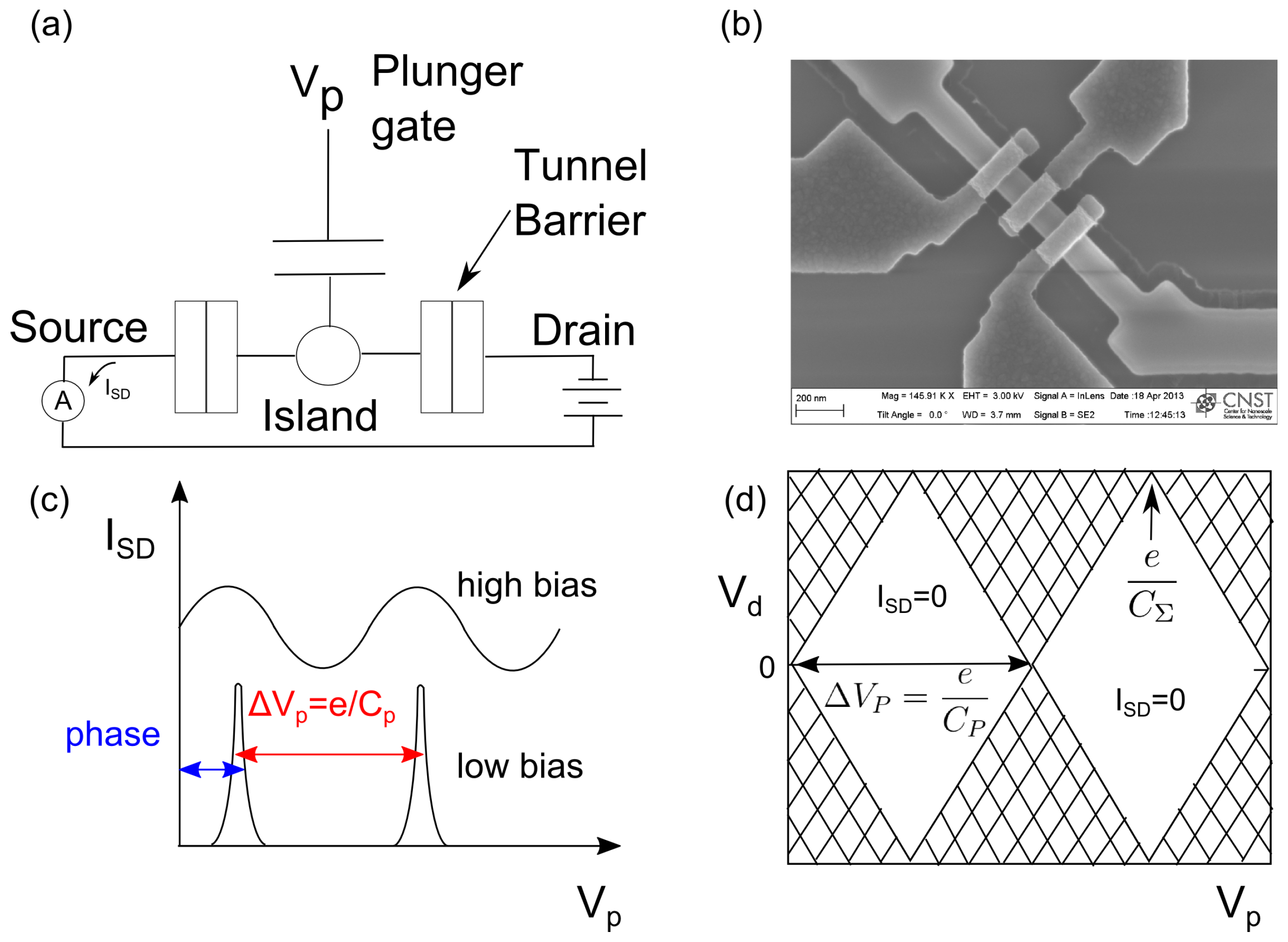
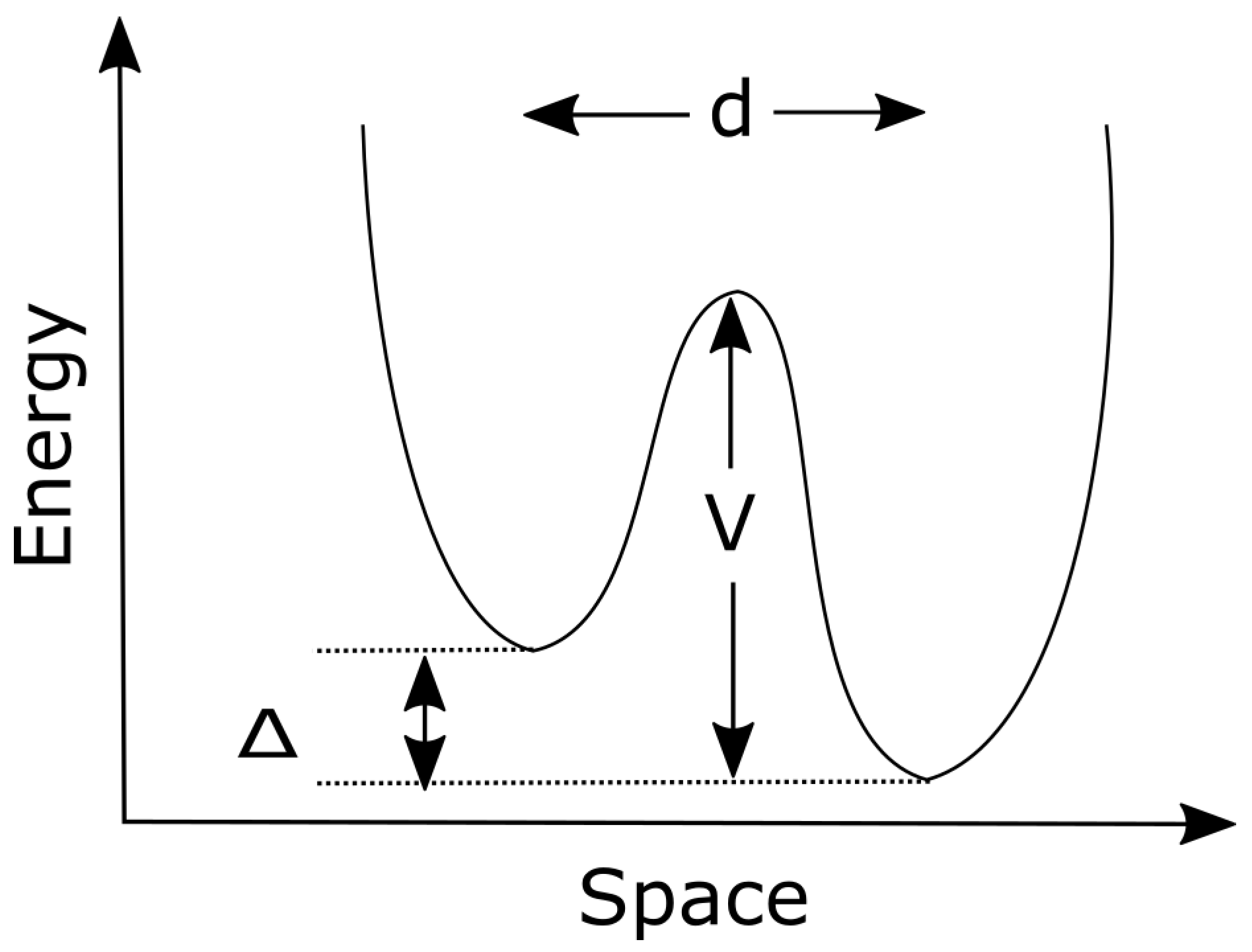
Figure 1a shows a circuit diagram representation of an SED. The tunnel barriers define an isolated island whose charge can only be changed by an integer number of electrons. As shown in the figure, the SED is a three terminal device where the gate electrode primarily controls the electrostatic potential of the island. Figure 1b shows an SEM image of one type of SED fabricated in silicon. The device consists of an etched and oxidized silicon nanowire with three finger gates wrapping around the device. These gates are used to form electrostatic tunnel barriers while an upper gate covering the wire from source to drain provides carriers (not shown). Dots are formed between the finger gates. The center finger gate can act as a barrier (to form two dots) or as a plunger gate when one dot is formed. Because the island is small, its total capacitance to the other electrodes is small. This implies a measurable electrostatic energy barrier for adding an additional electron to the island, E C = e 2 / C Σ . E C is known as the charging energy and produces a ladder of chemical potential levels on the island separated by E C . Transport is only allowed when one or more of the dot levels falls within the source-drain bias window, e V D . At low source-drain bias only one charging level may fit in the bias window and one measures current resonances, between which the number of electrons on the island is fixed. This is shown schematically in Figure 1c. The capacitance between the island and the plunger gate determines the spacing in voltage between the peaks. As the source-drain bias is increased, one reaches a point where more than one charging level is in the source-drain bias window and transport is no longer blockaded. This occurs when V D passes the top or bottom of the diamonds shown in Figure 1d. Therefore, the height of the diamonds allows measurement of the charging energy. At high bias, rather than measuring current resonances with zero current between them, the current oscillates sinusoidally without reaching zero current as shown in Figure 1c. The period of the oscillations is again defined by the gate capacitance, C P . The current oscillates, increasing as a new level enters the bias window and decreasing as a level leaves the bias window. Since the plunger gate capacitance is determined by the geometry, the period of oscillations as a function of V P are as well. Thus, the period of oscillations is a consequence of the geometry of the device and can be simulated accurately through electrostatic solver tools such as Fastcap [28]. Therefore, two identically fabricated devices should have very nearly the same period in the single electron curve.
While the period of the single electron curve should be very similar in different, but identically fabricated devices, the phase of the curve is not. Since the single electron oscillations are a function of gate voltage the phase corresponds to a voltage offset between successively measured curves. The difference in phase has its origin in the contribution from the local charge environment [29]. This is known as the charge offset, Q 0 phase Δ V P e . Devices fabricated simultaneously will exhibit different values of Q 0 because the local charge environment is randomly determined by the different processing steps such as gate oxidation, etching, dopant distribution, anneals, etc. However, so long as the local charge environment remains stable, the voltage on the plunger gate can be used to compensate for this difference and each device can be brought into phase. If instead, the local charge environment changes with time, then the phase of the device will fluctuate randomly in time and such phase synchronization becomes essentially impossible. In this case, the device exhibits charge offset drift, Δ Q 0 . In principle, the fluctuations in the local charge environment may occur at any frequency. Usually, the literature focuses on what is called the “long-term charge offset drift” which occurs at frequencies <1 Hz because the amplitude of the fluctuations is so large. This lack of synchronization, and concomitant difficulty in integration, drives our interest in studying Δ Q 0 .
Measurements of charge offset drift are not difficult to make, though care must be taken to make sure that the measurement circuit and wiring are such that they do not artificially inflate the level of charge offset drift recorded. There are two typical measurement setups for quantifying the level of charge offset drift in a particular device [30]. In the first method, a set of Coulomb blockade oscillations are repeatedly measured with a time delay between each measurement. Each curve is then fit to a sinusoidal function of the form
I D ( V P ) = A 0 + A sin [ 2 π ( V P / Δ V P + Q 0 ( t ) / e ) ] + B V P .
In the above, A 0 corresponds to a current offset, while A corresponds to the size of the oscillations, and Δ V P is the period of the oscillations as previously discussed. B may be used to account for any slope in the sinusoidal curve. The phase, Q 0 ( t ) in the fit is extracted and represents the charge offset drift. This is the most common measurement method. The second method is to measure the change in plunger gate voltage necessary to keep the current constant on a device (i.e., to keep a constant operating point in Figure 1). Regardless of the method used, the data are usually presented such that the voltage variation in the phase of the curves is normalized by the period of the oscillation so that Δ Q 0 ranges from 0 to 1e. These two methods can detect a Δ Q 0 0 . 01 e and Δ Q 0 0 . 001 e , respectively.
As has already been mentioned, charge offset drift precludes device integration. Conventional Complementary Metal Oxide Semiconductor (CMOS) logic devices are built in state-of-the-art cleanrooms so that the devices operate as uniformly as possible. If the threshold voltage of a metal-oxide-semiconductor field-effect transistor (MOSFET) varies significantly from one device to another, the devices cannot be integrated together. This is because a threshold voltage variation can result in a particular device’s on-state occurring outside the range of voltages available to switch it. The same effect can occur in SEDs through temporal variation of the turn-on characteristics of a device. If, as alluded to above, a current standard is to be built out of parallelized SEDs, then each device must be made to operate identically to reduce the tunneling errors that limit the accuracy of the device. If a standard is built from 100 devices each tuned so that the phase of their curves are synchronized with a desired error rate of 10 - 4 , then each device must be stable for at least 10 6 s or 12 days. Thus, it is clear that charge offset drift prohibits integration of SEDs in a way analogous to the way threshold voltage differences prohibit integration of conventional transistor devices [9]. It is worth mentioning that the 1 / f noise that typically occurs at f > 1 Hz in these devices does not limit the ability to parallelize devices such as for a current standard; only the large Δ Q 0 at f < 1 Hz precludes integration [31].
Charge offset drift also deleteriously affects work at the single device level. As a practical matter, keeping a single SED tuned in gate voltage space to exhibit the desired behavior becomes challenging over the experimental run time. For instance, a technique used in quantum computation known as spin-dependent tunneling is often used to read out the spin state of a single electron after having performed some manipulation [32,33,34]. The technique is illustrated in Figure 2. An applied magnetic field is used to split the spin states of the single electron charging level. To perform the readout one adjusts the voltage on the plunger gate to move the spin split chemical potentials of the dot so they straddle the Fermi level of a charge reservoir. If the spin on the dot is in the spin-up state, then the electron tunnels to the reservoir, while if it is in the spin down state, it does not tunnel. Thus, one infers the spin state from the charge dynmics. The readout level of the dot is carefully tuned to obtain the best fidelity in the readout process. In this case, charge offset drift will manifest itself in a lower readout fidelity since the fluctuations driving the charge offset drift will result in fluctuations of the readout level. To combat a moderate level of drift, automatic feedback has been implemented at the cost of increasing the complexity of the measurement [35].
Having seen how large values of Δ Q 0 can affect device operation and integration, we now move on in the next sections to catalog what has been measured and the empirical correlations between high and low values of Δ Q 0 .

2.1. Metal-Based Devices

In general, metal-based devices suffer from the worst charge offset drift behavior. Here, we are referring to devices fabricated from Al/AlOx/Al, where the AlOx provides the tunnel barriers shown in Figure 1a. These devices are typically fabricated through a technique known as double-angle evaporation [36]. A pattern is generated in electron beam resist through electron beam lithography and Al is evaporated at an angle. This Al is oxidized in a controlled environment within the deposition chamber, and then the deposition angle is changed. With a carefully designed pattern and the right angles, an SED is formed with AlOx tunnel barriers. Of course, devices have been fabricated from other metallic materials [37,38]. These devices can exhibit “clean” Coulomb diamonds without large jumps in the data characteristic of large charge offset drift while still exhibiting some low frequency time instability [39]. Unfortunately, we are unable to find rigorous measurements of charge offset drift, as outlined above, in metallic devices made from anything other than Al/AlOx. Therefore, we focus on Al/AlOx devices in this section.
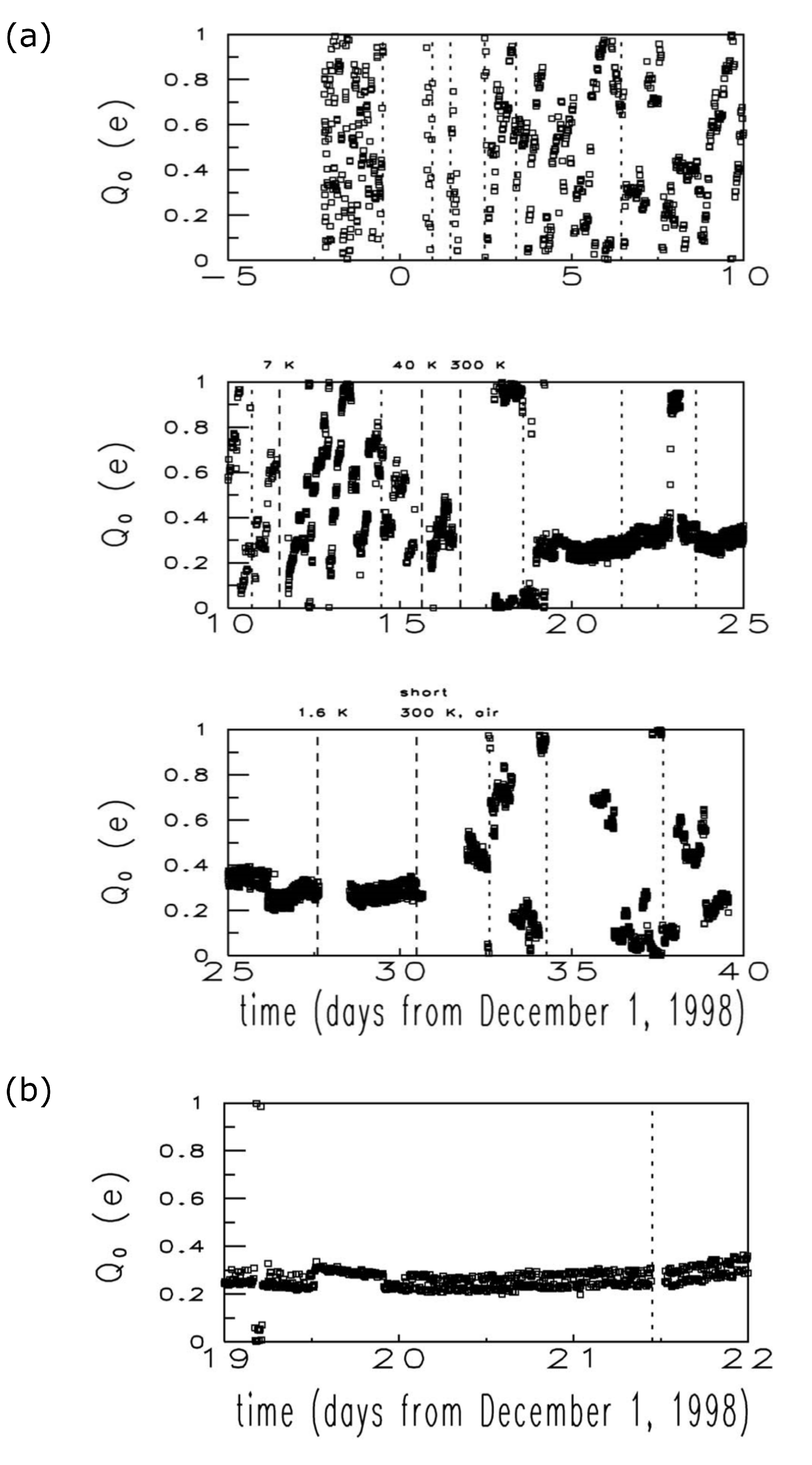
A typical measurement of the charge offset drift for a metallic device is shown in Figure 3a [30]. As is plainly apparent from the data, the charge offset value wanders between 0 and 1 e over the course of the measurement (and, in fact, probably wanders through several e). The time scale for the drift is on the order of minutes to hours. In addition, the data show periods of rapid evolution, some periods of relative stability, and sudden jumps. The evolution from a very rapidly changing charge offset value to one which subsequently changes more gradually or only with sudden steps, is known as “transient relaxation”. We will discuss this relaxation in more detail below. Figure 3b shows data that appear in Figure 3a between days 19 and 22. These data mainly consist of two distinct levels of Q 0 between 0.2 and 0.3. This indicates that the drift is driven by some switching behavior and will be discussed in more detail later. Finally, vertical dashed lines in the figure denote either mechanical disturbances or deliberate temperature excursions to investigate the temperature dependence, the effects of thermal cycling, or the effects of exposure to air. Mechanical changes such as refilling the dewar with liquid helium have no discernible effect. The same is true for temperature excursions up to 40 K. However, it is possible that thermally cycling the device up to room temperature and/or exposing it to air does change the qualitative nature of the charge offset drift measured.
Figure 4a shows source-drain current measured as a function of time through a metal-based SET for different values of the plunger gate voltage [40]. As the voltage on the plunger gate, V A , is increased, the fluctuations in the current become more rapid, while the amplitude and duty cycle remain constant. Looking closely at the data, one can see that it consists of discrete jumps, some of which appear as a quick succession of small steps and others which appear as a single large step. This is qualitatively similar to the data in Figure 3b where only two levels are seen. If each jump has its origin in the switching event of a single TLS, we can interpret jumps of different size as being due to defects at different distances from the dot with smaller jumps being due to defects further away from the dot.
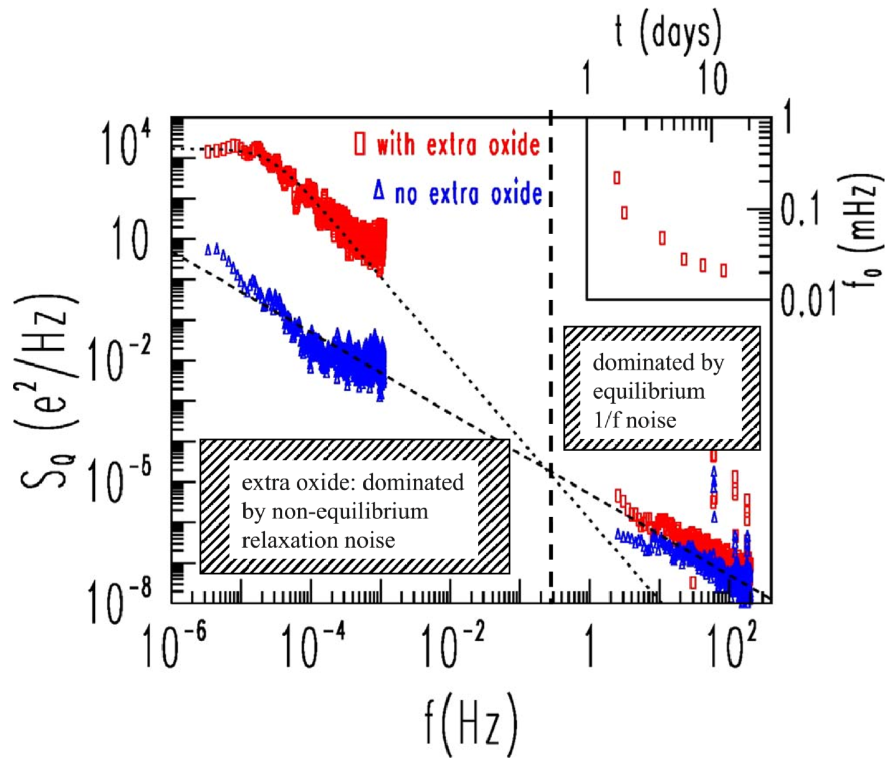
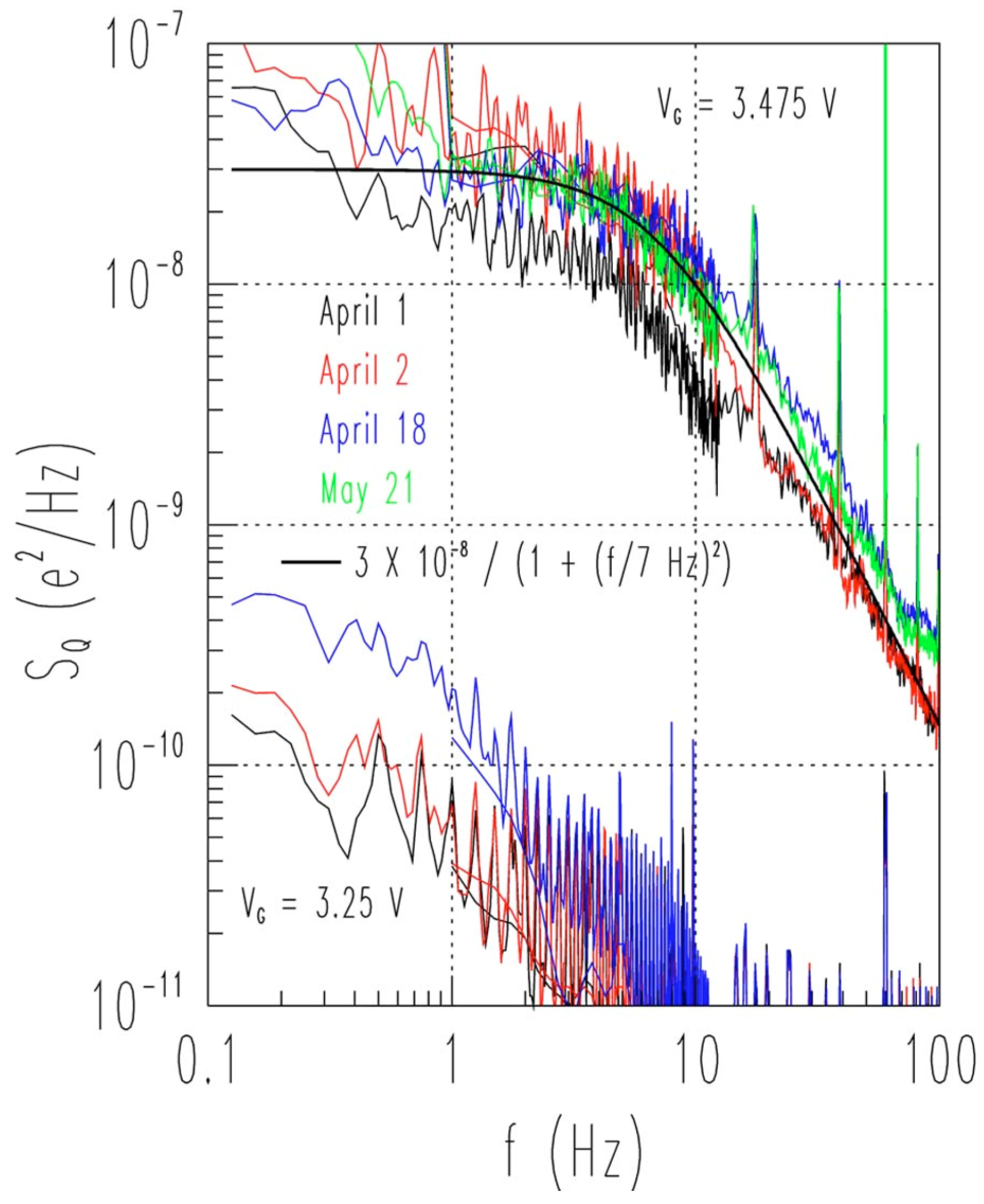
It is instructive to examine not only the time dependence but also the frequency dependence of the current noise in these devices. Examination of the power spectral density, S ( ω ) , allows us to separate equilibrium charge noise from non-equilibrium noise. S ( ω ) for the traces in Figure 4a is shown in Figure 4b along with a simulated set of data and Lorentzian fits. Consistent with the fits, the data show an approximately 1 / f 2 dependence over some frequency range (different for each curve). This indicates that the device is dominated by a single or few TLS. The power spectral density does not always follow 1 / f 2 at higher frequencies, however. In devices where the charge offset drift wanders continuously (without reproducible discrete jumps), the devices show a 1 / f dependence in the 1–100 Hz frequency range as shown in Figure 5. This is indicative of a large number of TLSs contributing to the charge noise in the device as a 1 / f spectrum results from the addition of a large number of 1 / f 2 spectra with different knee frequencies. This distinction separates devices into those dominated by a few defects or a single defect ( 1 / f 2 ), and those dominated by many ( 1 / f ).
The devices in reference [41] also show the transient relaxation present in Figure 3. The inset of Figure 5 shows that the characteristic frequency of the charge offset drift follows a 1 / t dependence, where t is the experimental run time. The 1 / t time dependence results in a long-tail evolution, which is characteristic of glassy relaxation, a non-equilibrium relaxation process. At frequencies above about 0.1 Hz, a 1 / f dependence is observed which does not change as a function of the experimental run time (not shown), indicating it is an equilibrium process.
Thus far, we have established that (i) the charge offset drift in metal devices is large; (ii) that the noise spectrum in some devices shows that nearby two-level systems (TLSs) participate; (iii) that charge offset drift events occur on the tens of minutes to hours time scale; and iv) that the drift at low frequencies can be a “long-tail” non-equilibrium process. Table 1, organized by device type, summarizes these results and the results for other types of devices discussed below. We can now discuss some attempts to mitigate Δ Q 0 by establishing some empirical correlations between the level of Δ Q 0 and some fabrication parameters or measurement protocols. Figure 5 shows the power spectral density for two different devices. The device plotted in red had extra oxide deposited on it to encapsulate the device while the blue device did not. This was done to investigate if the noise was associated with the presence of an amorphous insulator. Clearly, the blue curve’s low frequency noise is much lower than that of the red curve, indicating that this is indeed the case. Other tests have been performed, including: (i) metal deposition method (thermal vs e-beam); (ii) annealing in forming gas or inert gas; (iii) the use of ozone when forming tunnel junctions; (iv) thermal cycling to room temperature; (v) a nano-Faraday cage; (vi) cooling the device with or without electrical protection; and (vii) measuring in the normal vs. superconducting state. Unfortunately, none of these other tests substantially reduced the charge offset drift characteristics in metal devices [42].
The above are the basic characteristics of charge offset drift in metal devices. The features shown in the data of Figure 3, particularly that data of Figure 3b, indicate a two-level system as the dominant noise source contributing to Δ Q 0 . This conclusion is reinforced with the power spectral density data of Figure 4 and Figure 5. The spectrum shown in Figure 4 follows S Q 1 1 + f f 0 2 , indicating that these devices are dominated by a single or few TLSs. However, the short-term noise in Figure 5 is dominantly 1 / f in character.
It has already been shown that the defects can be associated with the presence of amorphous insulators [41]. Since metal devices are usually fabricated on insulating materials but also use AlOx to form the tunnel barriers, it is natural to ask in what part of the device these defects are typically located. Presumably, TLSs located anywhere near the device could change their charge by e and affect the charge offset noise. An appealingly simple argument by Song et al. [43] concludes that the dominant TLSs must be located in the tunnel barriers of the device. Since the electric field is largest in the tunnel barriers, the defects residing there would induce the largest change in the electrostatic potential of the island. Defects located elsewhere would experience far smaller fields and, therefore, be incapable of producing such large ( Δ Q 0 0 . 1 e ) excursions. Within this argument, monotonic or continuous drift would come from capacitively coupled defects located elsewhere but near the device and contribute to higher frequency 1 / f noise.
Several experiments attempt to locate the defects. The work of Zorin et al. [44] used two separate SEDs located 100 nm apart from each other and measured the low-frequency (1–10 Hz) correlations in the charge fluctuations. The expectation is that the experiment would find uncorrelated noise for defects entirely in the barrier and correlated noise for defects residing in the substrate (sputter deposited Al2O3). They found an appreciable level of correlation between the devices, as much as 20%. Thus, this experiment shows that the level of noise coming from the substrate material is comparable to that coming from the barriers and renders the argument of Song et al. incomplete.
The experiment depicted in Figure 4 (ref. [40]) also located the defects outside of the tunnel barriers by comparing the switching rates as a function of the plunger gate voltage to that expected for TLSs located in the barriers. As can be seen in the inset of Figure 4b, the switching rate is a monotonic and roughly exponential function of the gate voltage. This is in contrast to the voltage across a tunnel junction in the device, which should have a periodic dependence on gate voltage with period e / C g = 0 . 4 mV for this device. Whatever the identity and the functional form of the defects’ switching rate, the dependence on gate voltage should have some periodic character and not a large-scale dependence as shown. Thus, many of the defects contributing to Δ Q 0 are outside the tunnel barriers. Additionally, the data were found to be consistent with a cluster of TLSs which switched coherently when triggered by a particular TLS switch. The relative influence of a TLS on neighboring TLSs will play a crucial role in distinguishing between the behavior of metal and silicon-based devices.

2.2. Silicon-Based Devices

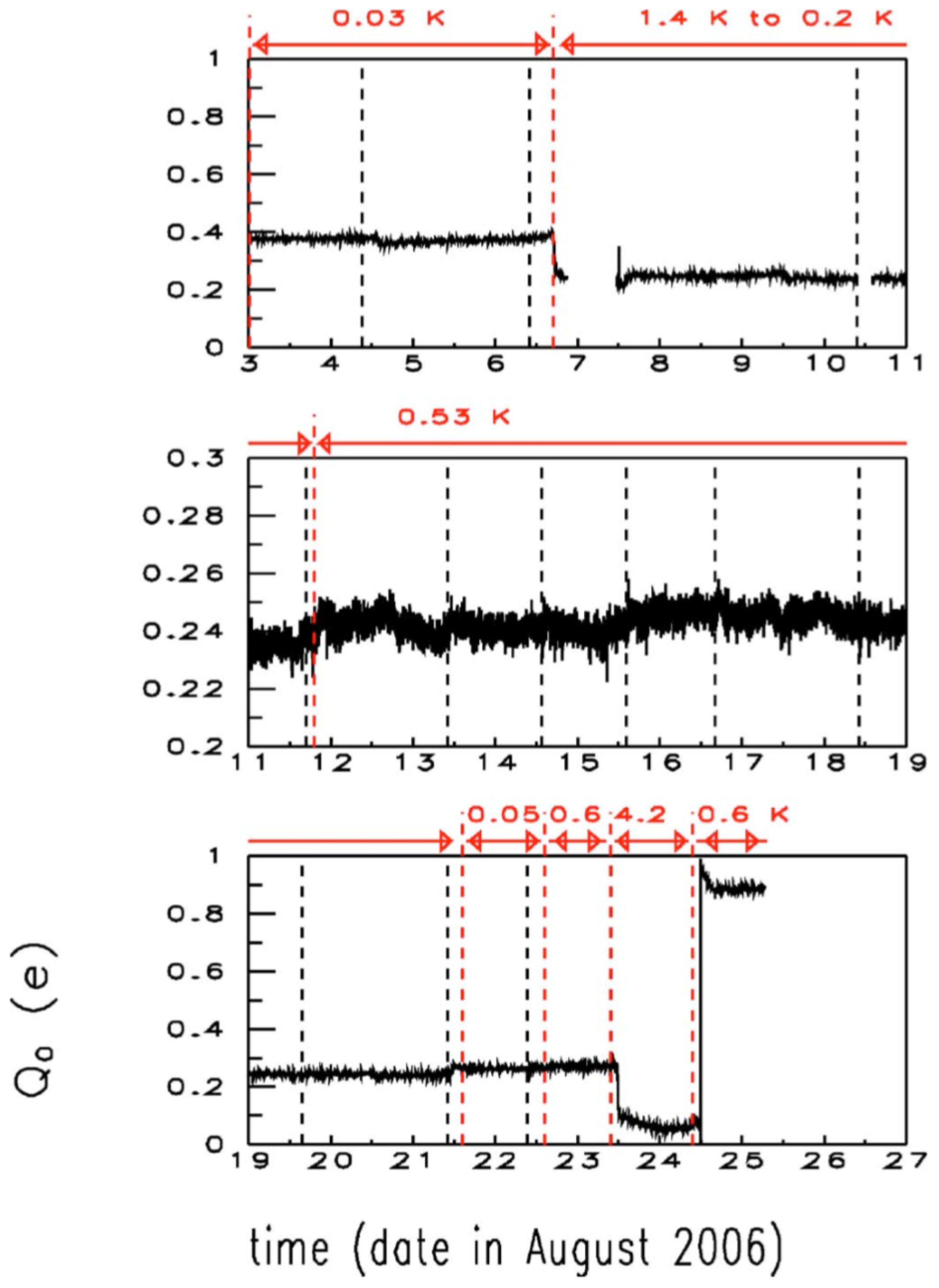
While metal-based devices show a large amount of drift and the transient relaxation phenomenon, all-silicon devices show neither effect. Silicon-based devices are usually fabricated through gate oxidation and etching of one or more layers of doped polySi gates to both form tunnel barriers in the silicon and provide carriers. A typical charge offset drift curve for an all-silicon device is shown in Figure 6 [45]. Here, the device exhibits Δ Q 0 0 . 01 e over the course of 15 days when the temperature is stable (middle panel and left side of lower panel). These data were measured in a device with electrostatically tunable tunnel barriers defined by a set of gates and their voltages (see Figure 1b). The same level of drift is seen in devices with fixed tunnel barriers prepared through a pattern dependent oxidation technique (PADOX) [31]. This remarkable difference between silicon-only devices and metallic devices will be explained below.
Figure 6 does show some non-idealities in the device performance when all the experimental factors are not held fixed. Vertical red dashed lines represent temperature changes and black dashed lines represent liquid helium transfers and, therefore, a mechanical disturbance to the device. There is very little, if any, change in Q 0 as a result of the mechanical disturbances for this device. However, abrupt changes in temperature can produce a measurable change in Q 0 .
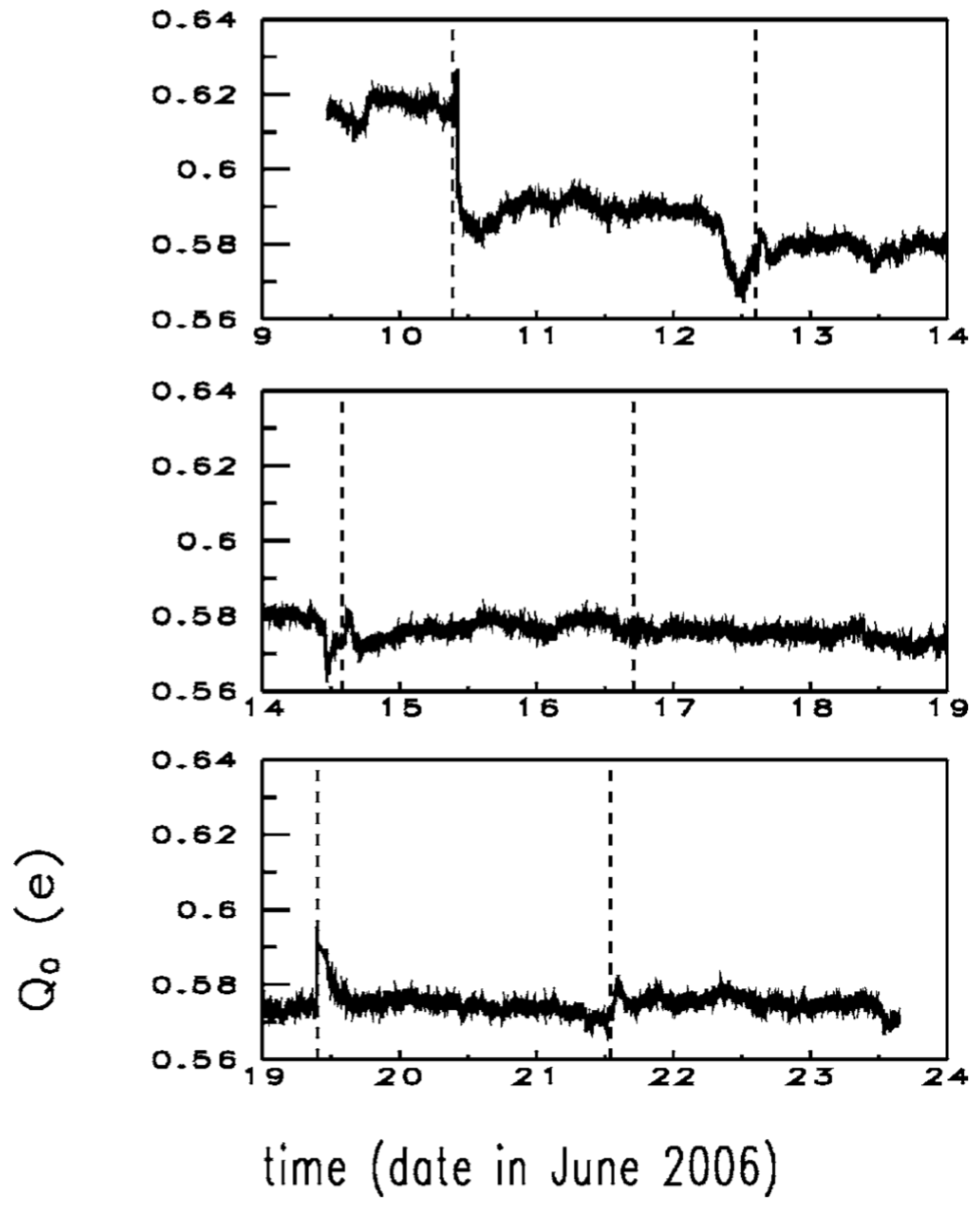
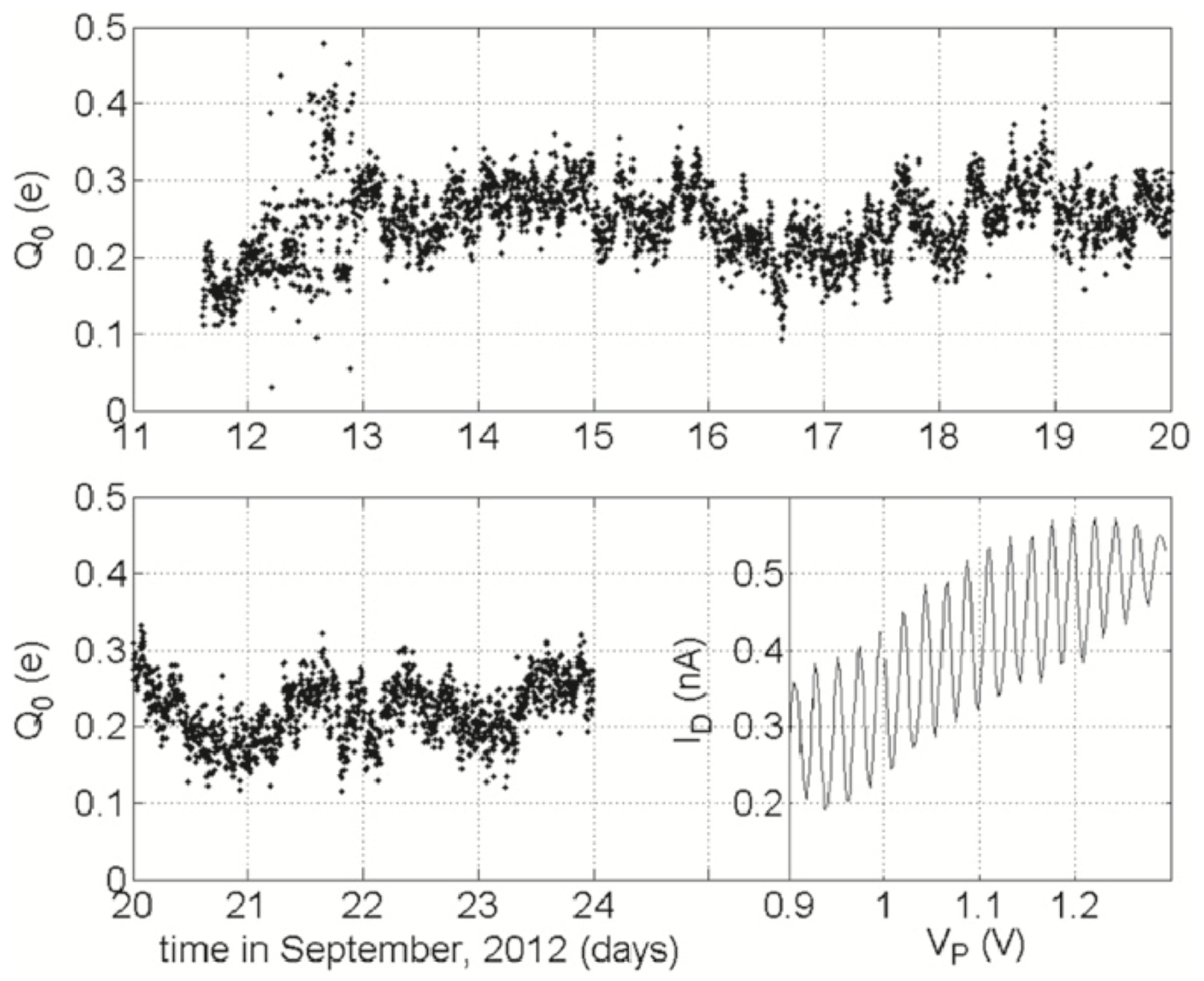
Figure 7 depicts the drift measured in another device from [45]. Here, the temperature was held between 20 to 40 mK during the entirety of the measurement. Black lines here also represent the mechanical disturbance of helium transfers. These data are plotted on a similar y-scale to that of the middle panel of Figure 6 and do exhibit some sensitivity to helium transfers.
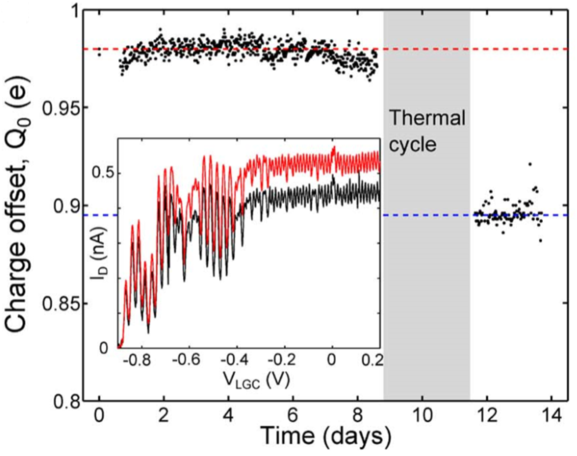
Though these devices are very stable, from the above data, it seems clear that all-silicon devices with electrostatic barriers are somewhat sensitive to temperature excursions and/or mechanical disturbances. In fact, these devices are also more sensitive than fixed-barrier PADOX devices [31]. This is probably a result of the increased number of gate voltages which are required to remain stable through mechanical or electrical disturbances in the tunable devices. However, this may depend on the details of fabrication since remarkable reproducibility has also been observed even after thermal cycling to room temperature [46] (see Figure 8 inset) or with months between measurements [30]. Thus, measurements of charge offset drift in the time domain reveal all-silicon devices (PADOX or electrostatic barrier devices) to be much more stable than metal devices. These results are summarized in Table 1.
To further the discussion of the stability of all-silicon devices, and to compare more completely to metal based devices, we can examine the power spectral density of the charge noise in these devices as well. Figure 9 shows data measured on various days and at two different gate voltages [30]. First, it is clear from the data at each gate voltage that the time dependence of the noise is quite small as the different color curves lie on top of each other for a particular gate voltage. Both the knee frequency and the absolute value of the noise remain unchanged. Secondly, one notices a difference in the character of the noise at V G = 3 . 475 V (upper cluster of curves) and V G = 3 . 25 V (lower cluster of curves). S Q shows a Lorentzian lineshape at V G = 3 . 475 V as evinced by the 1 / f 2 dependence above 10 Hz and the flat value of the noise below 1 Hz. The black line in the figure denotes a fit to this form. Therefore, in this range of gate voltage, there is a single TLS present in the device which dominates the noise. At V G = 3 . 25 V, S Q exhibits 1 / f noise and has orders of magnitude smaller noise below 1 Hz. While the 1 / f noise form denotes that there are several TLSs active at this gate voltage, their combined effect is much smaller than the single TLS, which is active at the higher gate voltage. Finally, these data include multiple changes in gate voltage, and thermal cycling to room temperature. The implication of this data is that an individual TLS present in the Si/SiO2 system was stable as a function of temperature or slow changes in the gate voltage. Thus, the remarkable stability of all-silicon SEDs is due to a lack of interactions between individual TLSs and not to the complete absence of TLSs.
As mentioned earlier, all-silicon devices with fixed barriers (PADOX) are marginally more stable than those with electrostatic barriers. Given this slight dependence on architecture one might think that the overall stability of devices might be the product of some specific steps in the fabrication. This has been directly addressed in the literature, most directly in reference [47], where devices were fabricated in different foundries. It was found that the stability of all-silicon devices is a robust property of the materials. Regardless of how the devices are fabricated, even devices with relatively poor performance (gate leakage and unintentional barriers) exhibit excellent charge offset stability 100 times better than that of metal-based devices [47].
In summary, single electron devices based in the Si/SiO2 material system show much smaller charge offset drift ( Δ Q 0 0 . 01 e ) than metallic SEDs ( Δ Q 0 1 e ) and much smaller sensitivity to external perturbations such as temperature, mechanical disturbance, and voltage pulses. This stability is not associated with the lack of TLSs in SiO2 but rather with the degree of interaction between TLSs which are present in both AlOx and SiO2. Before we discuss the TLSs in these systems within the context of glassy relaxation, we first discuss work on SEDs fabricated in the combined system of silicon dots defined with Al gates to complete the experimental picture.

2.3. Mixed Devices

The observations of charge offset drift which have been enumerated so far paint a striking dichotomy between metal-based devices and silicon-based devices. This drives a measurement of charge offset drift on a device where the SED quantum dot is formed in silicon with Al gates [48]. Devices based on this architecture have been extremely successful as quantum information devices and have recently been used to demonstrate the first two-qubit gate in silicon [24]. Earlier, the same group fabricated SEDs within 100 nm of each other to use one as a sensor of charge transitions on the other [35]. To be sensitive, the sensor SED has to remain on the steep portion of the SED curve at low bias shown schematically in Figure 1. To combat the charge offset drift induced excursions in the operating point of the sensor, the authors implemented a computer-controlled feedback loop to return the sensor to the appropriate place on the sensor control curve.
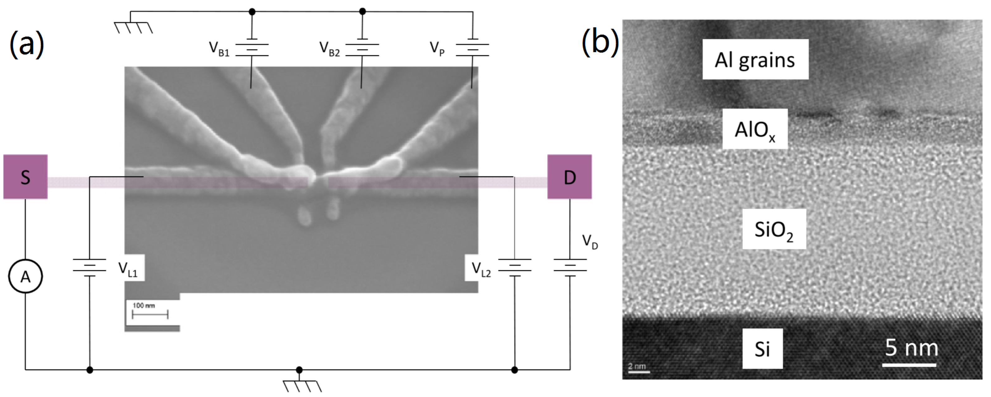
A similar device which contained only one SED was examined in reference [48]. The device is shown in an SEM micrograph in Figure 10a along with the measurement circuit. It consists of two barrier gates labeled B1 and B2. Two “lead gates” (labeled L1 and L2) provide carriers out to the heavily-doped source and drain without inducing a large number of electrons on the island. The island potential is modulated with the plunger gate labeled as P. The corresponding charge offset drift data appears in Figure 11. The size of the drift, Δ Q 0 0 . 15 e , is a value intermediate between that of silicon based devices and that of metal based devices. This is a powerful result. One might expect that since the dot is formed in the silicon away from the Al gates and the tunnel barriers are created electrostatically, that the charge offset drift would be similar to an all-silicon device. The fact that it is not similar lends strong support to the discussion of glassy relaxation. A hint as to why this is the case is shown in Figure 10b. It shows a TEM micrograph taken from a slice of the device along the line from source to drain under gate P, the dot plunger gate. As is clear from the micrograph, the deposited Al and SiO2 layer react to form a non-deliberate AlOx layer at the upper interface of the SiO2 gate dielectric. This is an important fabrication feature in determining the level of charge offset drift in the device.

2.4. Summary of Experimental Observations

Experimentally, it is clear that metal-based devices exhibit a large amount of charge offset drift Δ Q 0 1 e ), that silicon-only devices show very little ( Δ Q 0 0 . 01 e ), and that devices made in silicon with metallic gates show an intermediate level of drift ( Δ Q 0 0 . 15 e ).
Metal-based devices also show the phenomenon of transient relaxation that is correlated with the time from fabrication. More drift is also associated with the amount of amorphous insulator in or near the device. The frequency dependence of the charge offset drift noise in metal devices appears to be either 1 / f 2 in some devices or 1 / f in others. The former is correlated with observed steps or clusters of steps in the charge offset drift or current measured as a function of time, while the latter is correlated with a more continuous variation. This invites interpretation in terms of TLSs in the amorphous AlOx. These defects affect the device’s stability when they are found anywhere nearby as well as in the tunnel barriers of metal devices through their electrostatic coupling. Finally, while many experimental knobs have been turned to investigate correlations of charge offset drift with various fabrication and measurement parameters, they have revealed no correlations.
Silicon devices show very little charge offset drift even after thermal cycling, voltage pulses, and long periods of time between measurements. The relative lack of drift in silicon devices, combined with the observation of TLSs in certain energy ranges (temperature or gate voltage ranges), intimates that the crucial difference with metallic devices lies in the lack of interactions between TLSs in SiO2, not their absence.
Measurements on devices which combine the above material systems where the dot is formed in the silicon below a SiO2 gate dielectric with aluminum gates exhibit Δ Q 0 0 . 15 e . That these results occupy a middle ground between metallic and all-silicon devices, in combination with the observation of a non-deliberate AlOx layer below the gates, is consistent with the idea that the effect of TLSs reduces with distance from the dot.

3. Discussion

The most salient feature of the experimental review presented above is that, while both metallic devices and all-silicon devices have TLSs in the amorphous insulators that contribute to the charge noise, only metallic devices show a large charge offset drift. This difference in the behavior of the TLSs in each material system would appear to be explained by the lack of interaction between TLSs in the Si/SiO2 system, as evinced most directly by Figure 9. The TLSs in Si/SiO2 devices are stable over time, gate voltage, and thermal cycling.
Given the above influence of TLSs and the fact that the level of charge offset drift in metallic devices becomes more severe as the amount of amorphous insulating material increases (see Figure 5), it is natural to study the role of TLSs in these amorphous insulators. This field is known as glassy physics and is characterized by non-equilibrium relaxation. The relaxation is a consequence of structural relaxation due to tunneling in an array of TLSs. As an example, it is well-accepted that the long tail of heat released in calorimetry experiments on silica which show a 1 / t dependence [49] can be explained by this theory [50,51,52].
The characteristics of a TLS can be seen in Figure 12. Here, the asymmetry of the well is characterized by Δ, V is the tunneling barrier, and d represents the well separation.
The eigenstates of Figure 12 in the absence of tunneling are the position states | L and | R . In the presence of tunneling the eigenstates are linear combinations of | L and | R with energies E ± = ± Δ 2 + Δ 0 2 where Δ 0 = ω 0 e - λ is the tunnel coupling. These tunneling levels are coupled to electric fields [50], and we need only assume that some of these tunneling events are coupled electrostatically to the island of the SED and will contribute to charge offset drift to apply this model.
The above theory was adapted to estimate an upper bound on time scale over which charge offset in a metallic SED changes [30]. The rate of change of charge offset drift was found to be d N d t 0 . 3 h-1 or about one event every 3 h. This is in general agreement with the data on metallic devices and only applies to the transient relaxation phenomena in metallic devices. No theory of the equilibrium charge offset drift exists, and because glassy relaxation is a non-equilibrium theory, it cannot be directly applied to the equilibrium level of charge offset drift in metallic devices. However, the above agreement further validates an interpretation of charge offset drift in terms of interacting TLSs. Thus, it seems the high level of charge offset drift in metallic devices can be explained as a bath of interacting TLSs that are capable of inducing switching events in other TLSs. The crucial characteristic of the all silicon system would appear to be that the TLSs in SiO2 do not interact with each other.
It is clear that such TLSs exist in both AlOx and SiO2 from the data above; however, some detailed aspects of the microscopic origin of the TLS and what atoms are tunneling are not clear. It has been suggested that the origin of the TLS and the associated structural rearrangement through tunneling is either stress produced in deposition or the presence of OH ions [30] in metallic devices. In all-silicon devices, the origin of the TLSs may be caused by tetrahedra in the SiO2 reorienting or charging and discharging.

4. Conclusions

We have reviewed the experimental results on the low-frequency stability of SEDs known as charge offset drift in three classes of devices. This lack of stability stymies the use of SEDs in many applications, including as a current standard and as qubits, because it precludes integration of SEDs. This charge offset drift instability is most prominent in devices based on the Al/AlOx material system. It is essentially not present in SEDs fabricated entirely within the Si/SiO2 system. Moderate levels of Δ Q 0 are obtained in devices that combine the two material systems.
The origin of charge offset drift is revealed unambiguously by the power spectral density, S Q , of the noise to be TLS switching events. Distinct TLSs can be found in all-silicon devices by scanning through energy with either temperature or gate voltage. In small numbers, these defects result in a Lorentzian power spectrum. The level of interaction between TLS defects present in the amorphous insulators, AlOx and SiO2, accounts for the large difference in stability between devices fabricated in the different material systems. The TLSs in SiO2 are not triggered to switch by the switching behavior of other nearby TLSs, while those in AlOx interact and result in glassy relaxations of the material. A theory adapted from glassy relaxation qualitatively explains the observation of the non-equilibrium transient relaxation observed in metallic devices in addition to providing a numerical estimate of the frequency of charge offset drift switching events that is in general agreement with the experiments.
The prospects for overcoming the barrier to integration presented by large Δ Q 0 are unclear for metal based devices. Exploration of other material systems may be in order, though it is generally believed that metal oxides are much more defective than SiO2. There do not appear to be any obstacles to integrating all-silicon SEDs. The usual industry-standard techniques for maintaining excellent device uniformity though high-quality gate oxidation, forming gas anneals, and various cleaning procedures would appear to be enough to integrate these devices. While devices with dots residing in the silicon with Al gate electrodes show smaller drift than metallic devices, the level of drift will make direct integration of these devices a challenge. This is because an unintentional AlOx layer is formed at the interface between the SiO2 gate dielectric and the Al gate layer.
An interesting area for future work may be the use of silicide gates in the Si/SiO2 material system. Some silicides, when oxidized, form metallic oxides, while others form SiO2 [53]. Devices made in this way will help to reduce the resistance of gates made of polySi so that they can be operated at higher frequencies and may reduce the tendency of metallic gates to produce strain-induced barriers [54]. If those devices are also immune to the effects of charge offset drift, they may represent a large advance in the capability of current all-silicon based devices.

Author Contributions

M.D.S.J. organized and wrote the manuscript. N.M.Z. contributed to the scientific ideas and discussion.

Conflicts of Interest

The authors declare no conflict of interest.

References

  1. Keller, M.W.; Eichenberger, A.L.; Martinis, J.M.; Zimmerman, N.M. A Capacitance Standard Based on Counting Electrons. Science 1999, 285, 1706–1709. [Google Scholar] [CrossRef] [PubMed]
  2. Keller, M.W.; Martinis, J.M.; Zimmerman, N.M.; Steinbach, A.H. Accuracy of electron counting using a 7-junction electron pump. Appl. Phys. Lett. 1996, 69, 1804–1806. [Google Scholar] [CrossRef]
  3. Yamahata, G.; Nishiguchi, K.; Fujiwara, A. Gigahertz single-trap electron pumps in silicon. Nat. Commun. 2014, 5, 5038. [Google Scholar] [CrossRef] [PubMed]
  4. Fletcher, J.D.; Kataoka, M.; Giblin, S.P.; Park, S.; Sim, H.S.; See, P.; Ritchie, D.A.; Griffiths, J.P.; Jones, G.A.C.; Beere, H.E.; et al. Stabilization of single-electron pumps by high magnetic fields. Phys. Rev. B 2012, 86, 155311. [Google Scholar] [CrossRef]
  5. Giblin, S.P.; Kataoka, M.; Fletcher, J.D.; See, P.; Janssen, T.J.B.M.; Griffiths, J.P.; Jones, G.A.C.; Farrer, I.; Ritchie, D.A. Towards a quantum representation of the ampere using single electron pumps. Nat. Commun. 2012, 3, 930. [Google Scholar] [CrossRef] [PubMed]
  6. Yamahata, G.; Karasawa, T.; Fujiwara, A. Gigahertz single-hole transfer in Si tunable-barrier pumps. Appl. Phys. Lett. 2015, 106, 023112. [Google Scholar] [CrossRef]
  7. Nakamura, S.; Pashkin, Y.; Tsai, J.S.; Kaneko, N.H. Single-Electron Pumping by Parallel SINIS Turnstiles for Quantum Current Standard. IEEE Trans. Instrum. Meas. 2015, 64, 1696–1701. [Google Scholar] [CrossRef]
  8. Wright, S.J.; Blumenthal, M.D.; Pepper, M.; Anderson, D.; Jones, G.A.C.; Nicoll, C.A.; Ritchie, D.A. Parallel quantized charge pumping. Phys. Rev. B 2009, 80, 113303. [Google Scholar] [CrossRef]
  9. Maisi, V.F.; Pashkin, Y.A.; Kafanov, S.; Tsai, J.S.; Pekola, J.P. Parallel pumping of electrons. New J. Phys. 2009, 11, 113057. [Google Scholar] [CrossRef]
  10. Pekola, J.P.; Saira, O.P.; Maisi, V.F.; Kemppinen, A.; Möttönen, M.; Pashkin, Y.A.; Averin, D.V. Single-electron current sources: Toward a refined definition of the ampere. Rev. Mod. Phys. 2013, 85, 1421–1472. [Google Scholar] [CrossRef]
  11. Maeda, K.; Okabayashi, N.; Kano, S.; Takeshita, S.; Tanaka, D.; Sakamoto, M.; Teranishi, T.; Majima, Y. Logic Operations of Chemically Assembled Single-Electron Transistor. ACS Nano 2012, 6, 2798–2803. [Google Scholar] [CrossRef] [PubMed]
  12. Likharev, K.K. Single-electron devices and their applications. Proc. IEEE 1999, 87, 606–632. [Google Scholar] [CrossRef]
  13. Chen, R.H.; Korotkov, A.N.; Likharev, K.K. A new logic family based on single-electron transistors. In Proceedings of the 1995 53rd Annual Device Research Conference, Charlottesville, VA, USA, 19–21 June 1995; pp. 44–45.
  14. Takahashi, Y.; Ono, Y.; Fujiwara, A.; Inokawa, H. Silicon single-electron devices. J. Phys. Condens. Matter 2002, 14, R995. [Google Scholar] [CrossRef]
  15. Loss, D.; DiVincenzo, D.P. Quantum computation with quantum dots. Phys. Rev. A 1998, 57, 120. [Google Scholar] [CrossRef]
  16. Kane, B.E. A silicon-based nuclear spin quantum computer. Nature 1998, 393, 133–137. [Google Scholar] [CrossRef]
  17. Laird, E.A.; Pei, F.; Kouwenhoven, L.P. A valley-spin qubit in a carbon nanotube. Nat. Nanotechnol. 2013, 8, 565–568. [Google Scholar] [CrossRef] [PubMed]
  18. Petta, J.R.; Johnson, A.C.; Taylor, J.M.; Laird, E.A.; Yacoby, A.; Lukin, M.D.; Marcus, C.M.; Hanson, M.P.; Gossard, A.C. Coherent Manipulation of Coupled Electron Spins in Semiconductor Quantum Dots. Science 2005, 309, 2180–2184. [Google Scholar] [CrossRef] [PubMed]
  19. Medford, J.; Beil, J.; Taylor, J.M.; Rashba, E.I.; Lu, H.; Gossard, A.C.; Marcus, C.M. Quantum-Dot-Based Resonant Exchange Qubit. Phys. Rev. Lett. 2013, 111, 050501. [Google Scholar] [CrossRef] [PubMed]
  20. Brunner, R.; Shin, Y.S.; Obata, T.; Pioro-Ladriere, M.; Kubo, T.; Yoshida, K.; Taniyama, T.; Tokura, Y.; Tarucha, S. Two-Qubit Gate of Combined Single-Spin Rotation and Interdot Spin Exchange in a Double Quantum Dot. Phys. Rev. Lett. 2011, 107, 146801. [Google Scholar] [CrossRef] [PubMed]
  21. Koh, T.S.; Gamble, J.K.; Friesen, M.; Eriksson, M.A.; Coppersmith, S.N. Pulse-Gated Quantum-Dot Hybrid Qubit. Phys. Rev. Lett. 2012, 109, 250503. [Google Scholar] [CrossRef] [PubMed]
  22. Shi, Z.; Simmons, C.B.; Prance, J.R.; Gamble, J.K.; Koh, T.S.; Shim, Y.P.; Hu, X.; Savage, D.E.; Lagally, M.G.; Eriksson, M.A.; et al. Fast Hybrid Silicon Double-Quantum-Dot Qubit. Phys. Rev. Lett. 2012, 108, 140503. [Google Scholar] [CrossRef] [PubMed]
  23. Veldhorst, M.; Hwang, J.C.C.; Yang, C.H.; Leenstra, A.W.; Ronde, B.D.; Dehollain, J.P.; Muhonen, J.T.; Hudson, F.E.; Itoh, K.M.; Morello, A.; et al. An addressable quantum dot qubit with fault-tolerant control-fidelity. Nat. Nanotechnol. 2014, 9, 981–985. [Google Scholar] [CrossRef] [PubMed]
  24. Veldhorst, M.; Yang, C.H.; Hwang, J.C.C.; Huang, W.; Dehollain, J.P.; Muhonen, J.T.; Simmons, S.; Laucht, A.; Hudson, F.E.; Itoh, K.M.; et al. A two-qubit logic gate in silicon. Nature 2015, 526, 410–414. [Google Scholar] [CrossRef] [PubMed]
  25. Pla, J.J.; Tan, K.Y.; Dehollain, J.P.; Lim, W.H.; Morton, J.J.L.; Zwanenburg, F.A.; Jamieson, D.N.; Dzurak, A.S.; Morello, A. High-fidelity readout and control of a nuclear spin qubit in silicon. Nature 2013, 496, 334–338. [Google Scholar] [CrossRef] [PubMed]
  26. Pla, J.J.; Tan, K.Y.; Dehollain, J.P.; Lim, W.H.; Morton, J.J.L.; Jamieson, D.N.; Dzurak, A.S.; Morello, A. A single-atom electron spin qubit in silicon. Nature 2012, 489, 541–545. [Google Scholar] [CrossRef] [PubMed]
  27. Fowler, A.G.; Mariantoni, M.; Martinis, J.M.; Cleland, A.N. Surface codes: Towards practical large-scale quantum computation. Phys. Rev. A 2012, 86, 032324. [Google Scholar] [CrossRef]
  28. Thorbeck, T.; Fujiwara, A.; Zimmerman, N.M. Simulating Capacitances to Silicon Quantum Dots: Breakdown of the Parallel Plate Capacitor Model. IEEE Trans. Nanotechnol. 2012, 11, 975–978. [Google Scholar] [CrossRef]
  29. Grabert, H.; Devoret, M.H. (Eds.) Single Charge Tunneling Coulomb Blockade Phenomena in Nanostructures; Plenum Press: New York, NY, USA, 1992; Volume 294.
  30. Zimmerman, N.M.; Huber, W.H.; Simonds, B.; Hourdakis, E.; Fujiwara, A.; Ono, Y.; Takahashi, Y.; Inokawa, H.; Furlan, M.; Keller, M.W. Why the long-term charge offset drift in Si single-electron tunneling transistors is much smaller (better) than in metal-based ones: Two-level fluctuator stability. J. Appl. Phys. 2008, 104, 033710. [Google Scholar] [CrossRef]
  31. Zimmerman, N.; Huber, W.; Fujiwara, A.; Takahashi, Y. Excellent charge offset stability in a Si-based single-electron tunneling transistor. Appl. Phys. Lett. 2001, 79, 3188–3190. [Google Scholar] [CrossRef]
  32. Elzerman, J.M.; Hanson, R.; Willems van Beveren, L.H.; Witkamp, B.; Vandersypen, L.M.K.; Kouwenhoven, L.P. Single-shot read-out of an individual electron spin in a quantum dot. Nature 2004, 430, 431–435. [Google Scholar] [CrossRef] [PubMed]
  33. Morello, A.; Pla, J.J.; Zwanenburg, F.A.; Chan, K.W.; Huebl, H.; Mottonen, M.; Nugroho, C.D.; Yang, C.; van Donkelaar, J.A.; Alves, A.D.C.; et al. Single-shot readout of an electron spin in silicon. Nature 2010, 467, 687–691. [Google Scholar] [CrossRef] [PubMed]
  34. Watson, T.F.; Weber, B.; House, M.G.; Buch, H.; Simmons, M.Y. High Fidelity Rapid Initialization and Read-out of an Electron Spin via the Single Donor D Charge State. Phys. Rev. Lett. 2015, 115, 166806. [Google Scholar] [CrossRef] [PubMed]
  35. Yang, C.H.; Lim, W.H.; Zwanenburg, F.A.; Dzurak, A.S. Dynamically controlled charge sensing of a few-electron silicon quantum dot. AIP Adv. 2011, 1, 042111. [Google Scholar] [CrossRef]
  36. Fulton, T.A.; Dolan, G.J. Observation of single-electron charging effects in small tunnel junctions. Phys. Rev. Lett. 1987, 59, 109. [Google Scholar] [CrossRef] [PubMed]
  37. Okabayshi, N.; Maeda, K.; Tanaka, D.; Sakamoto, M.; Teranishi, T.; Majima, Y. Uniform charging energy of single-electron transistors by using size-controlled Au nanoparticles. Appl. Phys. Lett. 2012, 100, 033101. [Google Scholar] [CrossRef]
  38. Azuma, Y.; Yasutake, Y.; Kono, K.; Kanehara, M.; Teranishi, T.; Majima, Y. Single-Electron Transistor Fabricated by Two Bottom-Up Processes of Electroless Au Plating and Chemisorption of Au Nanoparticle. Jpn. J. Appl. Phys. 2010, 49, 090206. [Google Scholar] [CrossRef]
  39. Kano, S.; Azuma, Y.; Tanaka, D.; Sakamoto, M.; Teranishi, T.; Smith, L.W.; Smith, C.G.; Majima, Y. Random telegraph signals by alkanethiol-protected Au nanoparticles in chemically assembled single-electron transistors. J. Appl. Phys. 2013, 114, 223717. [Google Scholar] [CrossRef]
  40. Zimmerman, N.M.; Cobb, J.L.; Clark, A.F. Modulation of the charge of a single-electron transistor by distant defects. Phys. Rev. B 1997, 56, 7675–7678. [Google Scholar] [CrossRef]
  41. Zimmerman, N.M.; Huber, W.H. Microscope of glassy relaxation in femtogram samples: Charge offset drift in the single electron transistor. Phys. Rev. B 2009, 80, 195304. [Google Scholar] [CrossRef]
  42. Huber, W.; Martin, S.; Zimmerman, N. Long-term charge offset noise in Coulomb-Blockade devices. In Experimental Implementation of Quantum Computation; Clark, R., Ed.; Rinton Press, INC: Princeton, NJ, USA, 2001; pp. 176–182. [Google Scholar]
  43. Song, D.; Amar, A.; Lobb, C.J.; Wellstood, F.C. Advantages of superconducting Coulomb-blockade electrometers. IEEE Proc. Appl. Supercond. 1995, 5, 3085–3089. [Google Scholar] [CrossRef]
  44. Zorin, A.B.; Ahlers, F.J.; Niemeyer, J.; Weimann, T.; Wolf, H.; Krupenin, V.A.; Lotkhov, S.V. Background charge noise in metallic single-electron tunneling devices. Phys. Rev. B 1996, 53, 13682–13687. [Google Scholar] [CrossRef]
  45. Zimmerman, N.M.; Simonds, B.J.; Fujiwara, A.; Ono, Y.; Takahashi, Y.; Inokawa, H. Charge offset stability in tunable-barrier Si single-electron tunneling devices. Appl. Phys. Lett. 2007, 90, 033507. [Google Scholar] [CrossRef]
  46. Koppinen, P.J.; Stewart, M.D.; Zimmerman, N.M. Fabrication and Electrical Characterization of Fully CMOS-Compatible Si Single-Electron Devices. IEEE Trans. Electron Devices 2013, 60, 78–83. [Google Scholar] [CrossRef]
  47. Hourdakis, E.; Wahl, J.A.; Zimmerman, N.M. Lack of charge offset drift is a robust property of Si single electron transistors. Appl. Phys. Lett. 2008, 92, 062102. [Google Scholar] [CrossRef]
  48. Zimmerman, N.M.; Yang, C.H.; Lai, N.S.; Lim, W.H.; Dzurak, A.S. Charge offset stability in Si single electron devices with Al gates. Nanotechnology 2014, 25, 405201. [Google Scholar] [CrossRef] [PubMed]
  49. Zimmermann, J.; Weber, G. Thermal Relaxation of Low-Energy Excitations in Vitreous Silica. Phys. Rev. Lett. 1981, 46, 661–664. [Google Scholar] [CrossRef]
  50. Black, J.L. Relationship between the time-dependent specific heat and the ultrasonic properties of glasses at low temperatures. Phys. Rev. B 1978, 17, 2740–2761. [Google Scholar] [CrossRef]
  51. Anderson, P.W.; Halperin, B.I.; Varma, C.M. Anomalous low-temperature thermal properties of glasses and spin glasses. Philos. Mag. 1972, 25, 1–9. [Google Scholar] [CrossRef]
  52. Phillips, W. Tunneling states in amorphous solids. J. Low Temp. Phys. 1972, 7, 351–360. [Google Scholar] [CrossRef]
  53. Strydom, W.; Lombaard, J. Thermal oxidation of the silicides CoSi2, CrSi2, NiSi2, PtSi, TiSi2, and ZrSi2. Thin Solid Films 1985, 131, 215–231. [Google Scholar] [CrossRef]
  54. Thorbeck, T.; Zimmerman, N.M. Formation of strain-induced quantum dots in gated semiconductor nanostructures. AIP Adv. 2015, 5. [Google Scholar] [CrossRef]
Figure 1. (a) electrical diagram representation of a single electron device (SED); (b) scanning electron micrograph (SEM) of a silicon SED. The micrograph shows an etched and oxidized silicon nanowire with three wraparound finger gates made of doped polySi used to create barriers and form dots. An upper gate (not shown) provides the carriers and stretches from source to drain of the device; (c) coulomb blockade oscillations as a function of the plunger gate voltage depicted at high and low bias, V D . The phase is indicated and leads to our definition of Q 0 phase Δ V P e ; and (d) schematic of Coulomb diamonds (current measured as a function of plunger gate voltage and drain bias). The hatched areas exhibit non-zero source-drain current while the central diamonds show no current because the electrostatics fixes the number of electrons on the dot. The height of the diamonds gives the charging energy and the period in V p gives the capacitance between gate P and the dot.
Applsci 06 00187 g001
Figure 2. (a) schematic of single shot readout of a single phosphorus atom with an SED. Zeeman-split spin up electrons tunnel to the single electron transistor (SET) giving a current pulse while spin down electrons do not tunnel since that process is energetically uphill and do not give a current pulse on the SET. Reproduced with permission from reference [33], Copyright 2010, Nature Publishing Group; (b) pulse sequence which loads an electron from the SET island (acting as a reservoir), reads the electron state, and then empties the donor to reinitialize. Current traces for different spin states. Reproduced with permission from reference [34], Copyright 2015, American Physical Society.
Applsci 06 00187 g002
Figure 3. (a) typical charge offset drift of metal (Al/AlOx/Al) devices. A large amount of drift is observed. Unlabeled vertical dashed lines correspond to either liquid helium transfers or accidental losses of data; (b) a zoomed in set of the data in (a) between days 19 and 22 showing the two distinct values of charge offset drifts in the device at this time. The data were recorded at 20 mK unless indicated in the figure with fine print above dashed lines. Reproduced with permission from reference [30], Copyright 2008, American Institute of Physics.
Applsci 06 00187 g003
Figure 4. (a) current fluctuations as a function of time and gate voltage in an Al/AlOx/Al device. The data are made up of steps or collections of steps from a single dominant defect. The frequency of steps increases with gate voltage while the amplitude and duty cycle remain the same; (b) power spectral density of the noise in (a) at selected gate voltages. The data show a Lorentzian, flat at low frequencies and 1 / f 2 at high frequencies, dependence with different knee frequencies. Data were obtained at a temperature of about 15 mK. Inset shows the characteristic time extracted from the Lorentzian fits showing a roughly exponential dependence on gate voltage. Reproduced with permission from reference [40], Copyright 1997, American Physical Society.
Applsci 06 00187 g004
Figure 5. Power spectral density of charge offset drift fluctuations for two metallic devices. The device which was encapsulated with oxide shows larger S Q at low frequency while the high frequency noise is similar. The blue curve also follows a 1 / f dependence at low frequencies indicating it is dominated by equilibrium noise. The inset shows the knee frequency as a function of the experimental run time. Data were obtained at a temperature of 25 mK. Reproduced with permission from reference [41], Copyright 2009, American Physical Society.
Applsci 06 00187 g005
Figure 6. Typical charge offset drift for an all silicon SED with electrostatically generated barriers. A very small amount of drift is observed. Note the vertical axis range in the middle plot. These data were taken while the temperature (indicated at the top of each panel for a range of data indicated by the double arrow) was stepped (each step is indicated by vertical red dashed lines) which shows the insensitivity of the silicon SED to temperature excursions. Black dashed lines represent liquid helium transfers into the cryostat and thus a mechanical disturbance. Reproduced with permission from reference [45], Copyright 2007, American Institute of Physics.
Applsci 06 00187 g006
Figure 7. Charge offset drift measured in an Si/SiO2 device with electrostatic barriers where the temperature was held constant between 20 to 40 mK. In general, very small drift is observed. Vertical dashed lines represent helium transfers and mechanical disturbances of the system where some change in Q 0 is seen. Note the y-scale is quite magnified. Reproduced with permission from reference [45], Copyright 2007, American Institute of Physics.
Applsci 06 00187 g007
Figure 8. The main panel shows charge offset drift data in an all silicon device with electrostatic barriers. Very stable behavior before and after a thermal cycle to room temperature (represented by the time spanned by the grey bar) is observed. The inset shows the source-drain current as a function of plunger gate voltage before (black curve) and after (red curve) the thermal cycle measured with exactly the same voltages on every gate. All features in the data before the thermal cycle are reproduced in the curve taken after the thermal cycle. The curves are offset for clarity. All data were taken at a temperature of about 2.2 K. Reproduced with permission from reference [46], Copyright 2013, Institute of Electrical and Electronics Engineers.
Applsci 06 00187 g008
Figure 9. Power spectral density of an Si/SiO2 device measured at two different gate voltages and over the course of two months including several thermal cycles. The upper cluster of curves at V G = 3 . 475 V, indicates that a single two-level system (TLS) dominates at this gate voltage. Orders of magnitude less noise is obtained at V G = 3 . 25 V. The black curve is a fit to a Lorentzian. Reproduced with permission from reference [30], Copyright 2008, American Institute of Physics.
Applsci 06 00187 g009
Figure 10. SED made in silicon with Al gates. (a) micrograph of the device and the measurement circuit used for the charge offset drift measurement; (b) TEM micrograph of the device along the source to drain direction directly under the plunger gate, P. The micrograph shows that a non-deliberate AlOx layer forms at the interface between the SiO2 gate oxide and the Al gates. Reproduced with permission from reference [48], Copyright 2014, Institute of Physics.
Applsci 06 00187 g010
Figure 11. Charge offset drift in the same device as in Figure 10. The size of the drift is Δ Q 0 0.15e, intermediate between all-silicon devices and Al/AlOx devices. The inset shows the Coulomb blockade oscillations which were used to extract the Δ Q 0 values. Data were obtained at a temperature of 2.2 K. Reproduced with permission from reference [48], Copyright 2014, Institute of Physics.
Applsci 06 00187 g011
Figure 12. The potential landscape for a two-level fluctuator. Each amorphous insulator has many such potential landscapes described by distributions in V, d, and Δ.
Applsci 06 00187 g012
Table 1. Table of typical charge offset drift values for the different device types discussed in this review.
Device TypeTypical Δ Q 0 Comments
Al/AlOx/Al>1eShows transient relaxation; Δ Q 0 larger with more oxide
Si dot; Al gates 0 . 15 e
all-Si PADOX 0 . 01 e
all-Si gated 0 . 01 e slightly more sensitivity to disturbances than PADOX; can be trained

