
Determining the Parameters of Importance of a Graphene Synthesis Process Using Design-of-Experiments Method


Abstract
:
1. Introduction
2. Methods
2.1. Design-of-Experiments
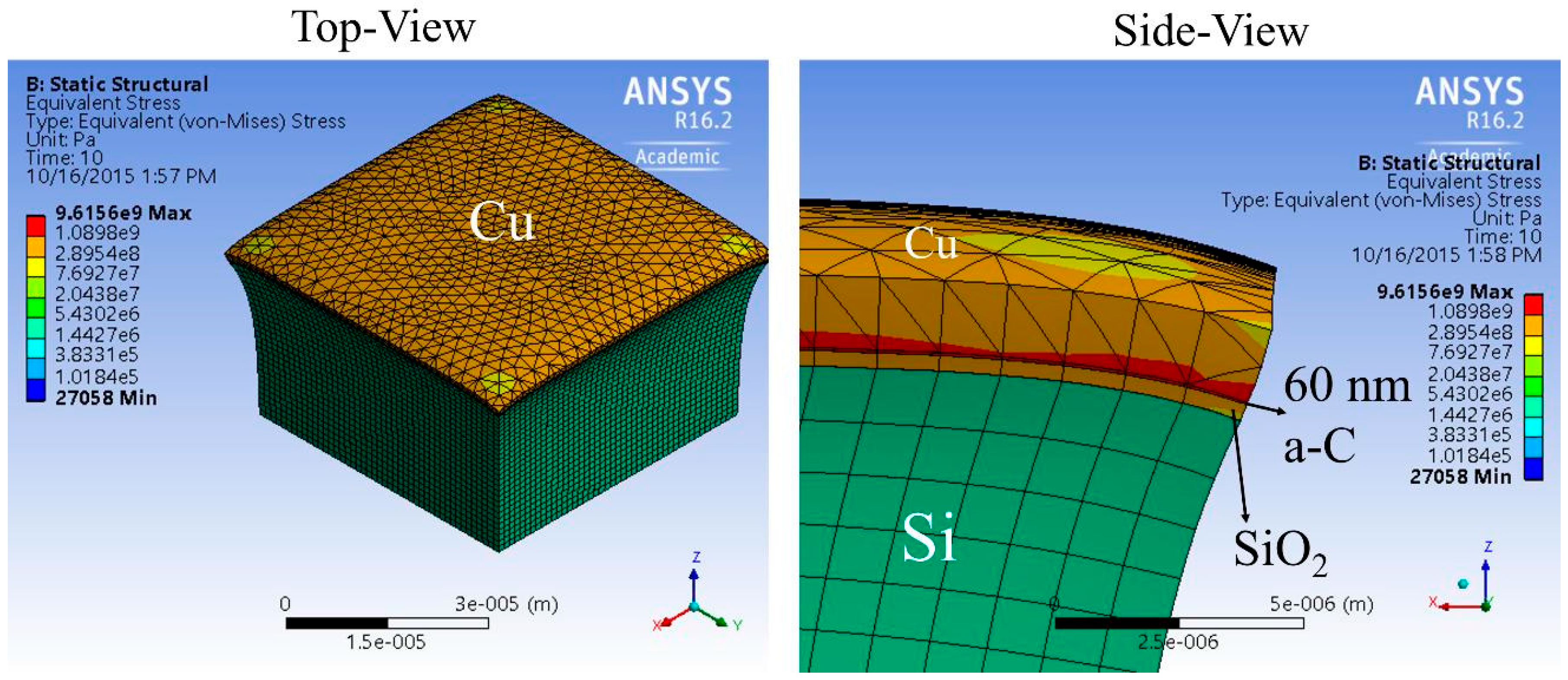
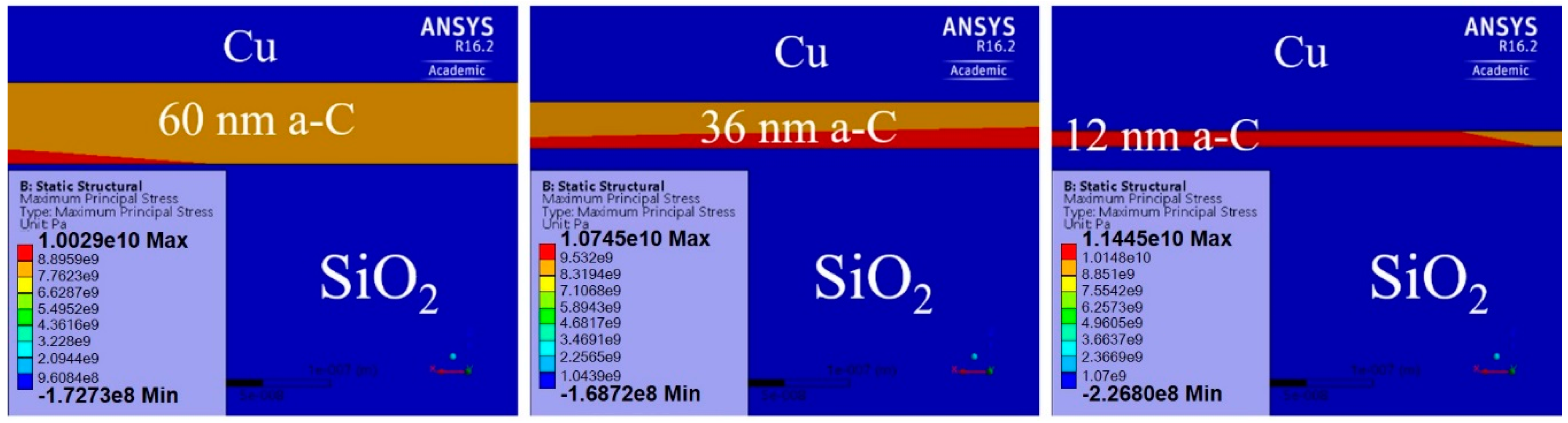
2.2. Graphene Synthesis
2.3. Characterization
3. Results and Discussions
3.1. Factorial Experiment Design and Experimental Results
3.2. DoE Analysis Results
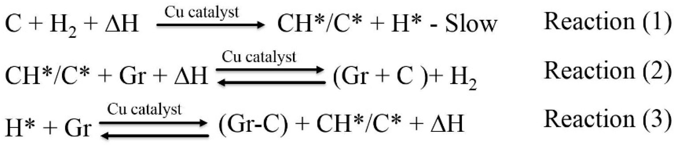
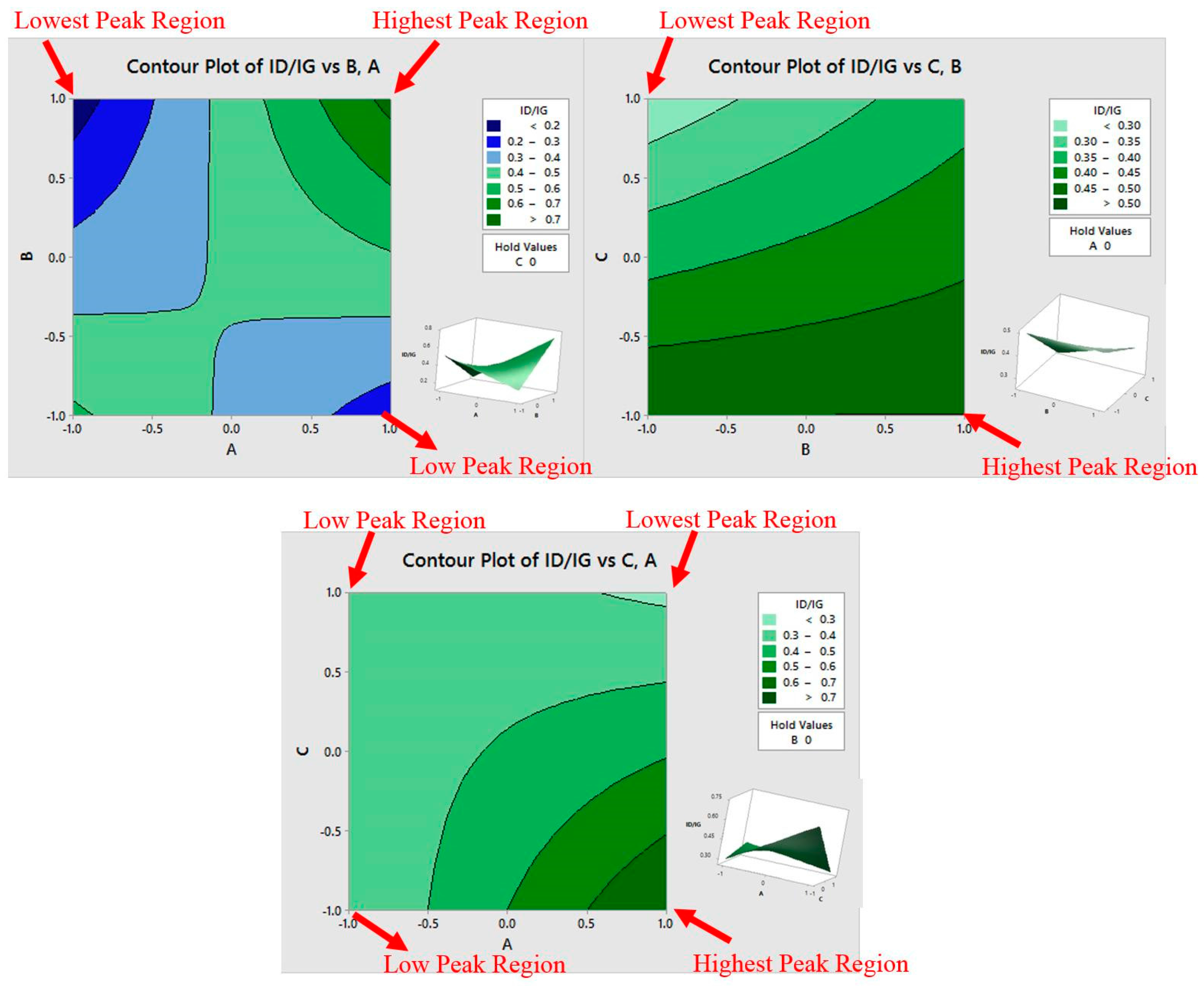
3.3. Physical Reasons of the Statistically-Significant Terms
3.4. Optimal Level of DoE Factors
3.5. Experimental Verification
4. Conclusions
Supplementary Materials
Acknowledgments
Author Contributions
Conflicts of Interest
References
- Novoselov, K.S.; Geim, A.K.; Morozov, S.V.; Jiang, D.; Zhang, Y.; Dubonos, S.V.; Grigorieva, I.V.; Firsov, A.A. Electric field effect in atomically thin carbon films. Science 2004, 306, 666–669. [Google Scholar] [CrossRef] [PubMed]
- Morozov, S.V.; Novoselov, K.S.; Katsnelson, M.I.; Schedin, F.; Elias, D.C.; Jaszczak, J.A.; Geim, A.K. Giant intrinsic carrier mobilities in graphene and its bilayer. Phys. Rev. Lett. 2008, 100, 016602. [Google Scholar] [CrossRef] [PubMed]
- Moser, J.; Barreiro, A.; Bachtold, A. Current-induced cleaning of graphene. Appl. Phys. Lett. 2007, 91, 163513. [Google Scholar] [CrossRef] [Green Version]
- Balandin, A.A.; Ghosh, S.; Bao, W.; Calizo, I.; Teweldebrhan, D.; Miao, F.; Lau, C.N. Superior thermal conductivity of single-layer graphene. Nano Lett. 2008, 8, 902–907. [Google Scholar] [CrossRef] [PubMed]
- Liu, Z.; Li, J.; Sun, Z.-H.; Tai, G.; Lau, S.-P.; Yan, F. The application of highly doped single-layer graphene as the top electrodes of semitransparent organic solar cells. ACS Nano 2012, 6, 810–818. [Google Scholar] [CrossRef] [PubMed]
- Zhu, X.-Z.; Han, Y.-Y.; Liu, Y.; Ruan, K.-Q.; Xu, M.-F.; Wang, Z.-K.; Jie, J.-S.; Liao, L.-S. The application of single-layer graphene modified with solution-processed TiOx and PEDOT:PSS as a transparent conductive anode in organic light-emitting diodes. Org. Electron. 2013, 14, 3348–3354. [Google Scholar] [CrossRef]
- Li, X.; Cai, W.; An, J.; Kim, S.; Nah, J.; Yang, D.; Piner, R.; Velamakanni, A.; Jung, I.; Tutuc, E.; et al. Large-area synthesis of high-quality and uniform graphene films on copper foils. Science 2009, 324, 1312–1314. [Google Scholar] [CrossRef] [PubMed]
- Eda, G.; Fanchini, G.; Chhowalla, M. Large-area ultrathin films of reduced graphene oxide as a transparent and flexible electronic material. Nat. Nanotechnol. 2008, 3, 270–274. [Google Scholar] [CrossRef] [PubMed]
- Kim, J.; Ishihara, M.; Koga, Y.; Tsugawa, K.; Hasegawa, M.; Iijima, S. Low-temperature synthesis of large-area graphene-based transparent conductive films using surface wave plasma chemical vapor deposition. Appl. Phys. Lett. 2011, 98, 091502. [Google Scholar] [CrossRef]
- Wang, J.; Liang, M.; Fang, Y.; Qiu, T.; Zhang, J.; Zhi, L. Rod-coating: Towards large-area fabrication of uniform reduced graphene oxide films for flexible touch screens. Adv. Mater. 2012, 24, 2874–2878. [Google Scholar] [CrossRef] [PubMed]
- Yan, Z.; Nika, D.L.; Balandin, A.A. Review of Thermal Properties of Graphene and Few-Layer Graphene: Applications in Electronics. Available online: https://arxiv.org/abs/1503.01825 (accessed on 12 July 2016).
- Shahil, K.M.F.; Balandin, A.A. Thermal properties of graphene and multilayer graphene: Applications in thermal interface materials. Solid State Commun. 2012, 152, 1331–1340. [Google Scholar] [CrossRef]
- Ballestar, A.; Esquinazi, P.; Barzola-Quiquia, J.; Dusari, S.; Bern, F.; da Silva, R.R.; Kopelevich, Y. Possible superconductivity in multi-layer-graphene by application of a gate voltage. Carbon 2014, 72, 312–320. [Google Scholar] [CrossRef]
- Chrissafis, K.; Bikiaris, D. Can nanoparticles really enhance thermal stability of polymers? Part I: An overview on thermal decomposition of addition polymers. Thermochim. Acta 2011, 523, 1–24. [Google Scholar] [CrossRef]
- Jia, Y.; Peng, K.; Gong, X.; Zhang, Z. Creep and recovery of polypropylene/carbon nanotube composites. Int. J. Plast. 2011, 27, 1239–1251. [Google Scholar] [CrossRef]
- Akbar, F.; Kolahdouz, M.; Larimian, S.; Radfar, B.; Radamson, H.H. Graphene synthesis, characterization and its applications in nanophotonics, nanoelectronics, and nanosensing. J. Mater. Sci. Mater. Electron. 2015, 26, 4347–4379. [Google Scholar] [CrossRef]
- Zhang, Y.; Zhang, L.; Zhou, C. Review of Chemical vapor deposition of graphene and related applications. Acc. Chem. Res. 2013, 46, 2329–2339. [Google Scholar] [CrossRef] [PubMed]
- Lee, H.C.; Liu, W.W.; Chai, S.P.; Mohamed, A.R.; Lai, C.W.; Khe, C.S.; Voon, C.H.; Hashim, U.; Hidayah, N.M.S. Synthesis of Single-layer Graphene: A review of recent development. Procedia Chem. 2016, 19, 916–921. [Google Scholar] [CrossRef]
- Choi, K.H.; Ali, A.; Jo, J. Randomly oriented graphene flakes film fabrication from graphite dispersed in N-methyl-pyrrolidone by using electrohydrodynamic atomization technique. J. Mater. Sci. Mater. Electron. 2013, 24, 4893–4900. [Google Scholar] [CrossRef]
- Macháč, P.; Fidler, T.; Cichoň, S.; Jurka, V. Synthesis of graphene on Co/SiC structure. J. Mater. Sci. Mater. Electron. 2013, 24, 3793–3799. [Google Scholar] [CrossRef]
- Ali Umar, M.I.; Yap, C.C.; Awang, R.; Hj Jumali, M.H.; Mat Salleh, M.; Yahaya, M. Characterization of multilayer graphene prepared from short-time processed graphite oxide flake. J. Mater. Sci. Mater. Electron. 2013, 24, 1282–1286. [Google Scholar] [CrossRef]
- Peng, K.J.; Lin, Y.H.; Wu, C.L.; Lin, S.F.; Yang, C.Y.; Lin, S.M.; Tsai, D.P.; Lin, G.R. Dissolution-and-reduction CVD synthesis of few-layer graphene on ultra-thin nickel film lifted off for mode-locking fiber lasers. Sci. Rep. 2015, 5. [Google Scholar] [CrossRef] [PubMed]
- Orofeo, C.M.; Ago, H.; Hu, B.; Tsuji, M. Synthesis of large area, homogeneous, single layer graphene films by annealing amorphous carbon on Co and Ni. Nano Res. 2011, 4, 531–540. [Google Scholar] [CrossRef]
- Reina, A.; Thiele, S.; Jia, X.; Bhaviripudi, S.; Dresselhaus, M.S.; Schaefer, J.A.; Kong, J. Growth of large-area single- and Bi-layer graphene by controlled carbon precipitation on polycrystalline Ni surfaces. Nano Res. 2009, 2, 509–516. [Google Scholar] [CrossRef] [Green Version]
- Wirtz, C.; Lee, K.; Hallam, T.; Duesberg, G.S. Growth optimisation of high quality graphene from ethene at low temperatures. Chem. Phys. Lett. 2014, 595, 192–196. [Google Scholar] [CrossRef]
- Nandamuri, G.; Roumimov, S.; Solanki, R. Chemical vapor deposition of graphene films. Nanotechnology 2010, 21, 145604. [Google Scholar] [CrossRef] [PubMed]
- Dong, X.; Wang, P.; Fang, W.; Su, C.-Y.; Chen, Y.-H.; Li, L.-J.; Huang, W.; Chen, P. Growth of large-sized graphene thin-films by liquid precursor-based chemical vapor deposition under atmospheric pressure. Carbon N. Y. 2011, 49, 3672–3678. [Google Scholar] [CrossRef]
- Srivastava, A.; Galande, C.; Ci, L.; Song, L.; Rai, C.; Jariwala, D.; Kelly, K.F.; Ajayan, P.M. Novel liquid precursor-based facile synthesis of large-area continuous, single, and few-layer graphene films. Chem. Mater. 2010, 22, 3457–3461. [Google Scholar] [CrossRef]
- Ji, H.; Hao, Y.; Ren, Y.; Charlton, M.; Lee, W.H.; Wu, Q.; Li, H.; Zhu, Y.; Wu, Y.; Piner, R.; et al. Graphene Growth Using a Solid Carbon Feedstock and Hydrogen. ACS Nano 2011, 5, 7656–7661. [Google Scholar] [CrossRef] [PubMed]
- Narula, U.; Tan, C.M.; Lai, C.S. Copper induced synthesis of graphene using amorphous carbon. Microelectron. Reliab. 2016, 61, 87–90. [Google Scholar] [CrossRef]
- Czitrom, V. One-Factor-at-a-Time Versus Designed Experiments. Am. Stat. Assoc. 1999, 53, 126–131. [Google Scholar]
- Montgomery, D.C.; Runger, G.C. Applied Statistics and Probability for Engineers; John Wiley & Sons: Hoboken, NJ, USA, 2010. [Google Scholar]
- Verma, S.; Lan, Y.; Gokhale, R.; Burgess, D.J. Quality by design approach to understand the process of nanosuspension preparation. Int. J. Pharm. 2009, 377, 185–198. [Google Scholar] [CrossRef] [PubMed]
- Kamal, N.; Cutie, A.J.; Habib, M.J.; Zidan, A.S. QbD approach to investigate product and process variabilities for brain targeting liposomes. J. Liposome Res. 2015, 25, 175–190. [Google Scholar] [CrossRef] [PubMed]
- Xu, X.; Khan, M.A.; Burgess, D.J. A quality by design (QbD) case study on liposomes containing hydrophilic API: I. Formulation, processing design and risk assessment. Int. J. Pharm. 2011, 419, 52–59. [Google Scholar] [CrossRef] [PubMed]
- Mei, K.-C.; Guo, Y.; Bai, J.; Costa, P.M.; Kafa, H.; Protti, A.; Hider, R.C.; Al-Jamal, K.T. Organic Solvent-Free, One-Step Engineering of Graphene-Based Magnetic-Responsive Hybrids Using Design of Experiment-Driven Mechanochemistry. ACS Appl. Mater. Interfaces 2015, 7, 14176–14181. [Google Scholar] [CrossRef] [PubMed]
- Vicente, G.; Coteron, A.; Martinez, M.; Aracil, J. Application of the factorial design of experiments and response surface methodology to optimize biodiesel production. Ind. Crops Prod. 1998, 8, 29–35. [Google Scholar] [CrossRef]
- Choudhury, I.A.; El-Baradie, M.A. Surface roughness prediction in the turning of high-strength steel by factorial design of experiments. J. Mater. Process. Technol. 1997, 67, 55–61. [Google Scholar] [CrossRef]
- Malard, L.M.; Pimenta, M.A.; Dresselhaus, G.; Dresselhaus, M.S. Raman spectroscopy in graphene. Phys. Rep. 2009, 473, 51–87. [Google Scholar] [CrossRef]
- Ferrari, A.C. Raman spectroscopy of graphene and graphite: Disorder, electron-phonon coupling, doping and nonadiabatic effects. Solid State Commun. 2007, 143, 47–57. [Google Scholar] [CrossRef]
- Ferrari, A.; Robertson, J. Resonant Raman spectroscopy of disordered, amorphous, and diamondlike carbon. Phys. Rev. B 2001, 64, 1–13. [Google Scholar] [CrossRef]
- Barker, T.B.; Milivojevich, A. Quality by Experimental Design; Chapman and Hall/CRC Press: Boca Raton, FL, USA, 2016. [Google Scholar]
- Spall, J. Factorial Design for Efficient Experimentation. IEEE Control Syst. Mag. 2010, 30, 38–53. [Google Scholar] [CrossRef]
- Jayakumar, M. Design of Experiments (DOE). Available online: https://www.isixsigma.com/tools-templates/design-of-experiments-doe/ (accessed on 20 May 2016).
- Montgomery, D.C. Design and Analysis of Experiments; John Wiley & Sons, Inc.: Hoboken, NJ, USA, 2013. [Google Scholar]
- Box, G.E.P.; Hunter, J.S.; Hunter, W.G. Statistics for Experimenters: Design, Innovation, and Discovery; Wiley-Blackwell: Hoboken, NJ, USA, 2005. [Google Scholar]
- Vlassiouk, I.; Regmi, M.; Fulvio, P.; Dai, S.; Datskos, P.; Eres, G.; Smirnov, S. Role of Hydrogen in Chemical Vapor Deposition Growth of Large Single-Crystal Graphene. ACS Nano 2011, 5, 6069–6076. [Google Scholar] [CrossRef] [PubMed]
- Yao, Y.; Li, Z.; Lin, Z.; Moon, K.-S.; Agar, J.; Wong, C. Controlled Growth of Multilayer, Few-Layer, and Single-Layer Graphene on Metal Substrates. J. Phys. Chem. C 2011, 115, 5232–5238. [Google Scholar] [CrossRef]
- Blech, I.; Cohen, U. Effects of humidity on stress in thin silicon dioxide films. J. Appl. Phys. 1982, 53, 4202–4207. [Google Scholar] [CrossRef]
- Marques, F.C.; Lacerda, R.G.; Champi, A.; Stolojan, V.; Cox, D.C.; Silva, S.R.P. Thermal expansion coefficient of hydrogenated amorphous carbon. Appl. Phys. Lett. 2003, 83, 3099–3101. [Google Scholar] [CrossRef] [Green Version]
- White, G.K. Thermal expansion of reference materials: Copper, silica and silicon. J. Phys. D Appl. Phys. 2002, 6, 2070–2078. [Google Scholar] [CrossRef]
- Kim, M.T. Influence of substrates on the elastic reaction of films for the microindentation tests. Thin Solid Films 1996, 283, 12–16. [Google Scholar] [CrossRef]
- Cho, S.; Chasiotis, I.; Friedmann, T.A.; Sullivan, J.P. Young’s modulus, Poisson’s ratio and failure properties of tetrahedral amorphous diamond-like carbon for MEMS devices. J. Micromech. Microeng. 2005, 15, 728–735. [Google Scholar] [CrossRef]
- Bloomfield, M.O.; Bentz, D.N.; Cale, T.S. Stress-Induced Grain Boundary Migration in Polycrystalline Copper. J. Electron. Mater. 2008, 37, 249–263. [Google Scholar] [CrossRef]
- Stoney, G.G. The Tension of Metallic Films Deposited by Electrolysis. Proc. R. Soc. A Math. Phys. Eng. Sci. 1909, 82, 172–175. [Google Scholar] [CrossRef]
- Xu, S.; Tay, B.K.; Tan, H.S.; Zhong, L.; Tu, Y.Q.; Silva, S.R.P.; Milne, W.I. Properties of carbon ion deposited tetrahedral amorphous carbon films as a function of ion energy. J. Appl. Phys. 1996, 79. [Google Scholar] [CrossRef]
- Yao, J.; Cahoon, J.R. Experimental studies of grain boundary diffusion of hydrogen in metals. Acta Metall. Mater. 1991, 39, 119–126. [Google Scholar] [CrossRef]
- Buehler, M.J.; Hartmaier, A.; Gao, H. Constrained grain boundary diffusion in thin copper films. MRS Proc. 2004, 821. [Google Scholar] [CrossRef]


| Levels | Factors | ||
|---|---|---|---|
| Annealing Temperature | a-C Layer Thickness | Annealing Time | |
| A | B | C | |
| −1 (Low) | 820 °C | 12 nm | 10 min |
| +1 (High) | 1020 °C | 36 nm | 50 min |
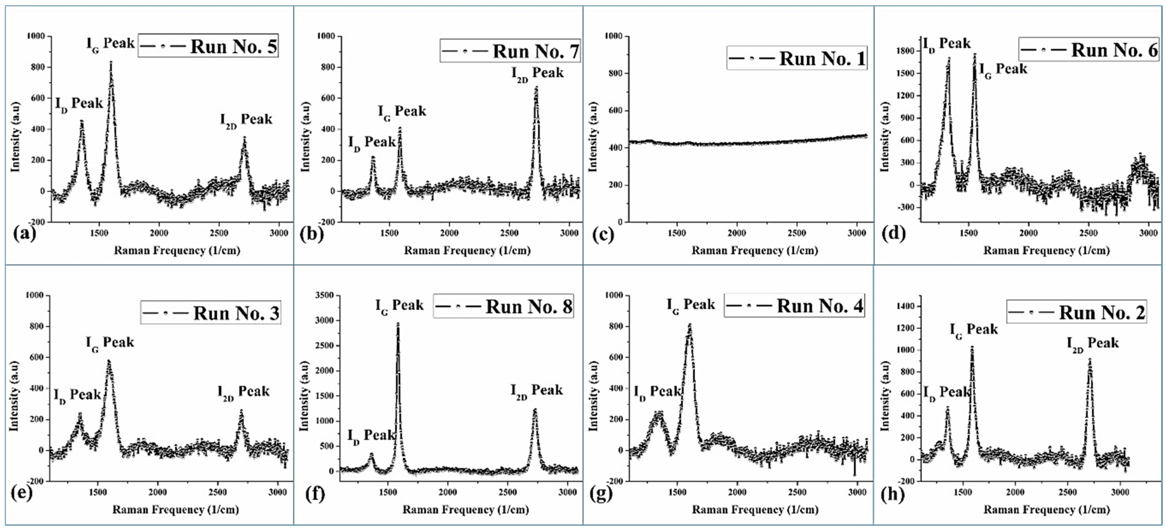
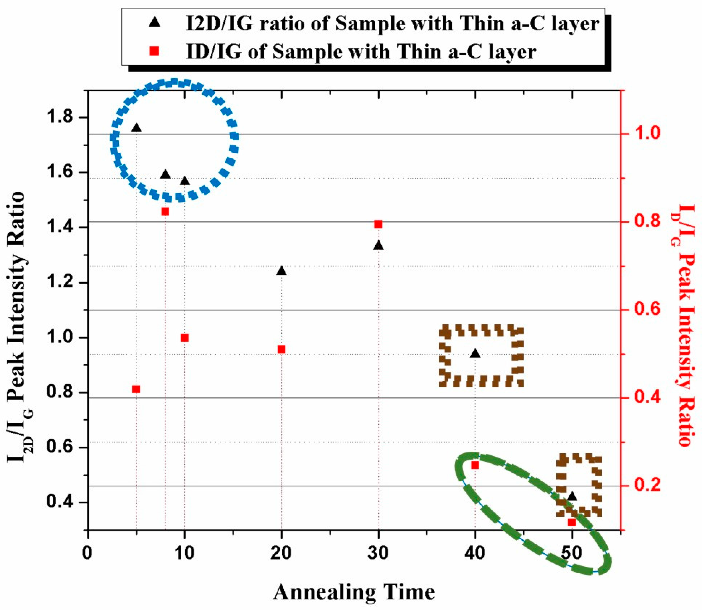
| Runs’ Order | Raman Spectrum in Figure 1 | Controlling Factors | Responses | |||
|---|---|---|---|---|---|---|
| Annealing Temperature | a-C Layer Thickness | Annealing Time | I2D/IG Peak Intensity Ratio (Response I) | ID/IG Peak Intensity Ratio (Response II) | ||
| A | B | C | ||||
| 5 | (a) | 820 °C | 12 nm | 10 min | 0.300 | 0.600 |
| 7 | (b) | 1020 °C | 12 nm | 10 min | 1.900 | 0.400 |
| 1 | (c) | 820 °C | 36 nm | 10 min | 0.001 | 0.001 |
| 6 | (d) | 1020 °C | 36 nm | 10 min | 0.001 | 1.000 |
| 3 | (e) | 820 °C | 12 nm | 50 min | 0.434 | 0.434 |
| 8 | (f) | 1020 °C | 12 nm | 50 min | 0.250 | 0.100 |
| 4 | (g) | 820 °C | 36 nm | 50 min | 0.001 | 0.300 |
| 2 | (h) | 1020 °C | 36 nm | 50 min | 0.890 | 0.464 |
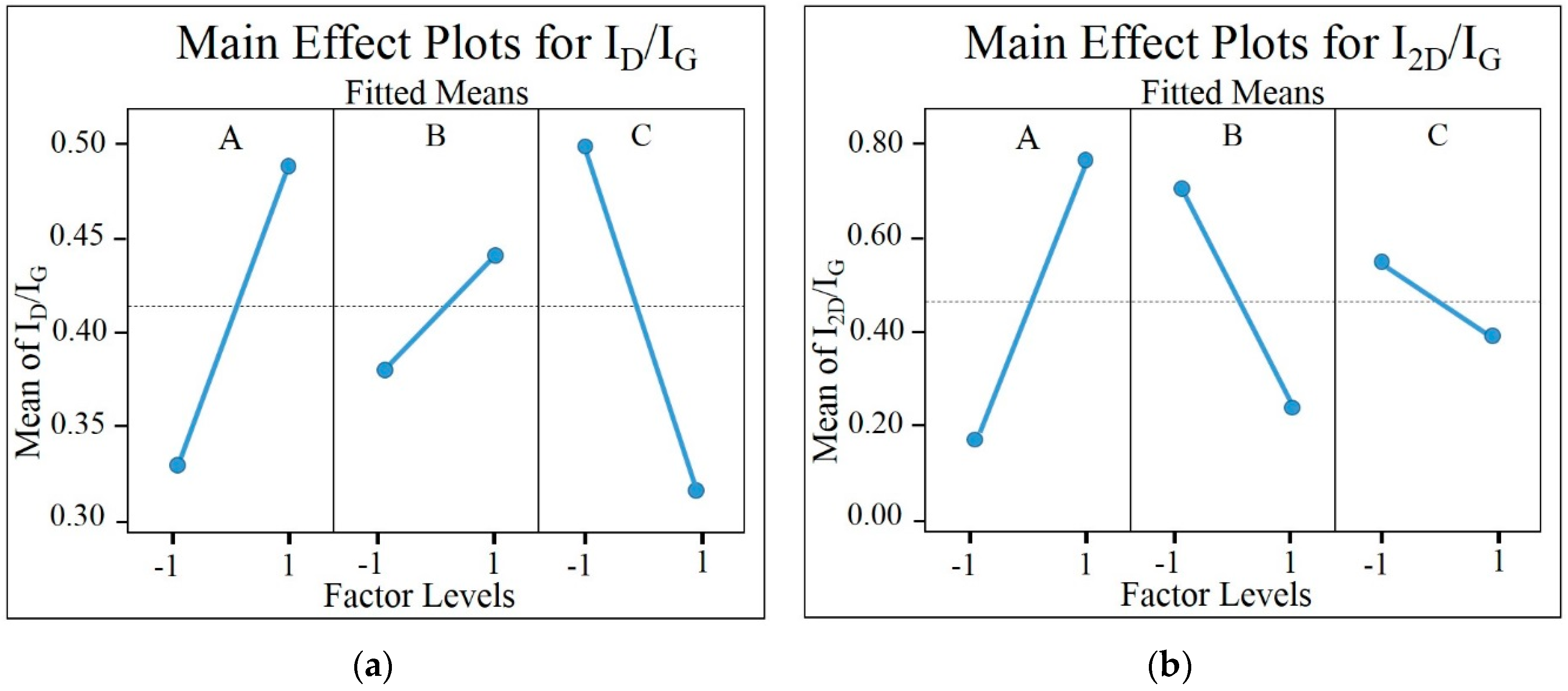
| Factors | Degrees of Freedom (DF) | Adjusted Sum of Squares (SS) | Adjusted Mean of Squares (MS) = SS/DF | F = MS/MSE | p | Contribution |
|---|---|---|---|---|---|---|
| Linear Effects | ||||||
| A | 1 | 0.0495 | 0.0495 | 0.65 | 0.445 | 7.46% |
| B | 1 | 0.0067 | 0.0067 | 0.09 | 0.775 | 1.01% |
| C | 1 | 0.0618 | 0.0618 | 0.80 | 0.396 | 9.31% |
| 2-way Interactions | ||||||
| AC | 1 | 0.1174 | 0.1174 | 1.53 | 0.251 | 17.70% |
| BC | 1 | 0.0066 | 0.0066 | 0.086 | 0.776 | 0.99% |
| Error | 8 | 0.6142 | MSE = 0.076 | - | - | 9.26% |
| Factors | Degree of Freedom (DF) | Adjusted Sum of Squares (SS) | Adjusted Mean of Squares (MS) = SS/DF | F = MS/MSE | p | Contribution |
|---|---|---|---|---|---|---|
| Linear Effects | ||||||
| C | 1 | 0.0491 | 0.0491 | 0.44 | 0.525 | 1.66% |
| 2-way Interactions | ||||||
| AB | 1 | 0.0347 | 0.0347 | 0.31 | 0.592 | 1.17% |
| AC | 1 | 0.1001 | 0.1001 | 0.90 | 0.371 | 3.38% |
| Error | 8 | 0.8931 | MSE = 0.111 | - | - | 30.18% |
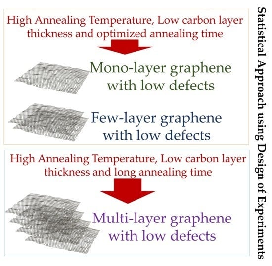
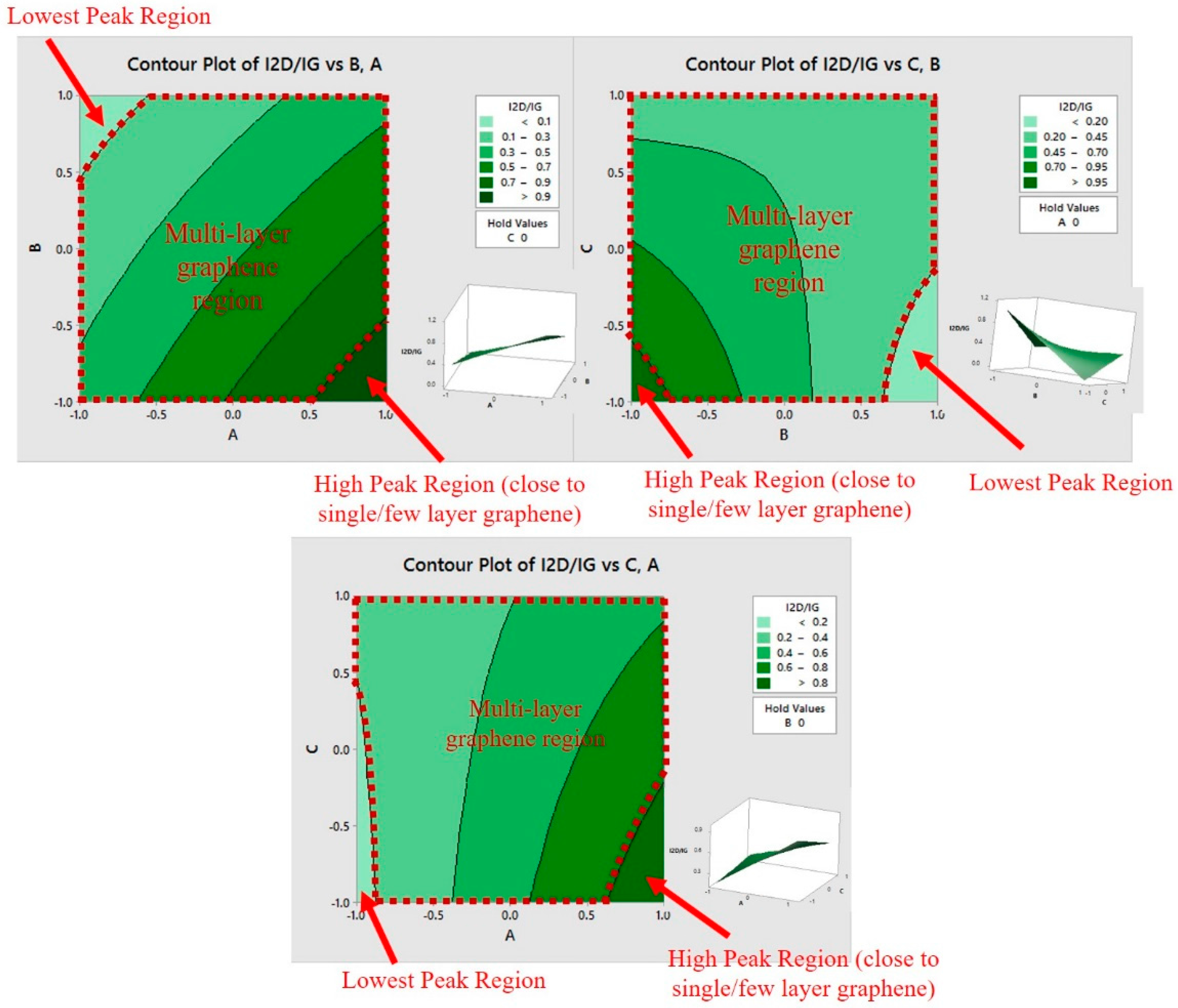
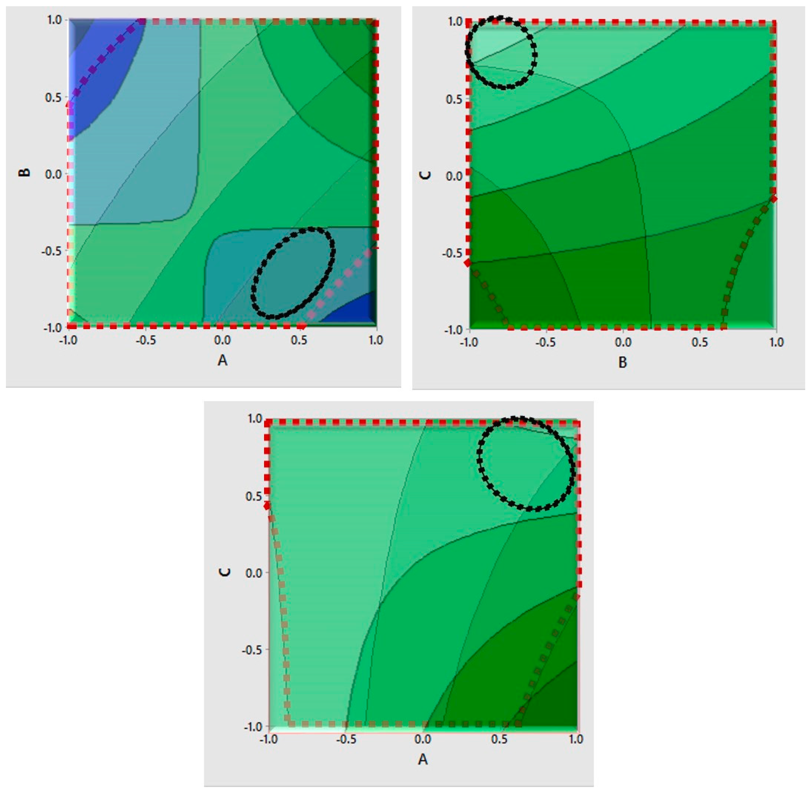
| Desired Graphene Traits | Respective Responses I & II | Factors | ||
|---|---|---|---|---|
| A Annealing Temperature | B a-C Layer Thickness | C Annealing Time | ||
| Low defects only | Low Response I | Low for high B; High for low B | Low | Large |
| Mono-/few-layer graphene only | High Response II | High | Low | Small |
| Mono-/few-layer graphene with low defects | Low Response I and high Response II | High | Low | Need to be optimized using response surface method [37,45] |
| Multi-/many-layer graphene only | Low Response II | Large region in Figure 8, representing several combinations | ||
| Multi-/many-layer graphene with low defects | Low Response I and low Response II | High | Low | Large |
| As indicated by Figure 9 | ||||
© 2016 by the authors; licensee MDPI, Basel, Switzerland. This article is an open access article distributed under the terms and conditions of the Creative Commons Attribution (CC-BY) license (http://creativecommons.org/licenses/by/4.0/).
Share and Cite
Narula, U.; Tan, C.M. Determining the Parameters of Importance of a Graphene Synthesis Process Using Design-of-Experiments Method. Appl. Sci. 2016, 6, 204. https://doi.org/10.3390/app6070204
Narula U, Tan CM. Determining the Parameters of Importance of a Graphene Synthesis Process Using Design-of-Experiments Method. Applied Sciences. 2016; 6(7):204. https://doi.org/10.3390/app6070204
Chicago/Turabian StyleNarula, Udit, and Cher Ming Tan. 2016. "Determining the Parameters of Importance of a Graphene Synthesis Process Using Design-of-Experiments Method" Applied Sciences 6, no. 7: 204. https://doi.org/10.3390/app6070204