
Plasmonic and Dielectric Metasurfaces: Design, Fabrication and Applications

Wuhan National Laboratory for Optoelectronics, School of Optical and Electronic Information, Huazhong University of Science and Technology, Wuhan 430074, China
*
Author to whom correspondence should be addressed.
Appl. Sci. 2016, 6(9), 239; https://doi.org/10.3390/app6090239
Submission received: 16 June 2016
/
Revised: 3 August 2016
/
Accepted: 10 August 2016
/
Published: 14 September 2016
(This article belongs to the Special Issue Nanophotonics and Quantum Optics of Hybrid Nanoparticle Systems: Applications and Fundamentals)
Abstract
:Two-dimensional metasurfaces are widely focused on for their ability for flexible light manipulation (phase, amplitude, polarization) over sub-wavelength propagation distances. Most of the metasurfaces can be divided into two categories by the material type of unit structure, i.e., plasmonic metasurfaces and dielectric metasurfaces. For plasmonic metasurfaces, they are made on the basis of metallic meta-atoms whose optical responses are driven by the plasmon resonances supported by metallic particles. For dielectric metasurfaces, the unit structure is constructed with high refractive index dielectric resonators, such as silicon, germanium or tellurium, which can support electric and magnetic dipole responses based on Mie resonances. The responses of plasmonic and dielectric metasurfaces are all relevant to the characteristics of unit structure, such as dimensions and materials. One can manipulate the electromagnetic field of light wave scattered by the metasurfaces through designing the dimension parameters of each unit structure in the metasurfaces. In this review article, we give a brief overview of our recent progress in plasmonic and dielectric metasurface-assisted nanophotonic devices and their design, fabrication and applications, including the metasurface-based broadband and the selective generation of orbital angular momentum (OAM) carrying vector beams, N-fold OAM multicasting using a V-shaped antenna array, a metasurface on conventional optical fiber facet for linearly-polarized mode (LP11) generation, graphene split-ring metasurface-assisted terahertz coherent perfect absorption, OAM beam generation using a nanophotonic dielectric metasurface array, as well as Bessel beam generation and OAM multicasting using a dielectric metasurface array. It is believed that metasurface-based nanophotonic devices are one of the devices with the most potential applied in various fields, such as beam steering, spatial light modulator, nanoscale-resolution imaging, sensing, quantum optics devices and even optical communication networks.
1. Introduction
A “metamaterial” is a man-made material whose properties can be attained by designing the unit structure, having been widely focused on for a dozen years since it was firstly reported by Smith et al. in 2000 [1]. The unit structure in metamaterial, called meta-atoms or meta-molecules, must be considerably smaller than the operating wavelength, and the distance between neighboring meta-atoms also has a subwavelength scale [2]. This subwavelength scale inhomogeneity makes the whole metamaterial uniform on the macro of performance, and this phenomenon makes this artificial structure essentially a “material” rather than a device. Therefore, one can arbitrarily arrange the so-called meta-atoms into periodic arrays to build one-dimensional (1D) materials (chains), two-dimensional (2D) materials (metasurfaces) and three-dimensional (3D) materials (metamaterials), as shown in Figure 1 [3]. For the metamaterial, one can even manipulate its macroscopical properties, such as permittivity ε and permeability μ. The research of metamaterials is essentially related to the exploitation of the electromagnetic parameter space for better control of electromagnetic waves, as depicted in Figure 1. Utilizing metamaterials, one can enter regions of the electromagnetic parameter space that are not observed in conventional material, but that are not forbidden by Maxwell’s equations, such as the third quadrant of the parameter space (negative-index materials), zero-index materials and the space far away from the non-magnetic line [4,5,6,7]. Taking advantage of these attractive features, as shown in Figure 1, metamaterials have been widely applied in optical negative index materials [8,9,10,11,12], nonlinear optics [13,14,15,16], optical magnetism [17,18,19], super resolution [20,21,22,23,24,25], giant artificial chirality [26,27], electromagnetic cloaks [28,29,30,31,32], etc.
Besides 3D materials, 2D metasurfaces are also widely focused on for their ability for flexible light manipulation (phase, amplitude, polarization) over subwavelength propagation distances [33,34,35,36,37]. Most of the metasurfaces can be divided into two categories by the material type of unit structure: plasmonic and dielectric, as displayed in Figure 2. For plasmonic metasurfaces, they are made on the basis of metallic meta-atoms whose optical responses are driven by the plasmon resonances supported by metallic particles. When a metallic particle is placed in an electric field, the conduction electrons escape from their equilibrium positions with respect to the core ions, resulting in a polarization of the particle and generating a depolarizing field. In a time-varying external field, this collective motion in the metallic particle can be seen as a Lorentzian oscillator whose characteristic peak in the displacement amplitude is around the resonance frequency and accompanied by a phase shift of π over the spectral width of the resonance [38,39,40,41,42,43,44,45,46]. For dielectric metasurfaces, the unit structure is constructed with high refractive index dielectric resonators, such as silicon, germanium or tellurium, which can support electric and magnetic dipole responses based on Mie resonances [47]. When a dielectric particle is illuminated by a light wave whose frequency is below or near the bandgap frequency of the material of particle, both the magnetic dipole (first Mie resonance) and electric dipole resonances (second Mie resonance) are excited. The magnetic and electric Mie resonance can then enhance the magnetic and electric field at the particle’s center at optical frequencies, respectively, and this enhancement is related to the intrinsic properties of dielectric particles [48,49,50,51,52,53,54,55,56,57,58]. Therefore, the responses of plasmonic and dielectric metasurfaces are all relevant to the characteristics of the unit structure, such as dimensions and materials. One can manipulate the electromagnetic field of the light wave scattered by the metasurfaces through designing the dimension parameters of each unit structure in the metasurfaces [59].
To produce the designed metasurfaces, many attractive previous works have reported the fabrication techniques, such as electron-beam lithography [60,61,62,63,64,65], focused-ion beam [66,67], interference lithography [68,69,70,71,72] and nanoimprint lithography [73,74,75,76,77]. Electron-beam lithography is a standard method that can fabricate the metasurface with high nanoscale resolution. Focused-ion beam is a more appropriate method for rapid prototyping. Interference lithography can provide a solution for realizing large-scaled metasurface fabrication. Nanoimprint lithography is a more promising technique for combining many advantages of the former, such as high-resolution, large-scaled production and low processing cost [73]. The unique properties and the development of fabrication techniques have allowed metasurfaces to be applied in various fields, such as flat optics [33,34,35,78,79,80,81,82,83,84,85,86,87,88,89,90,91,92,93,94,95,96,97,98,99,100], nonlinear effects [101,102,103,104,105,106,107], photonic Hall effects [108,109,110], electromagnetically-induced transparency [111], cloaking [112,113,114,115,116,117], etc., as shown in Figure 2. For instance, the applications of metasurfaces in the field of flat optics mainly include anomalous reflection/refraction [34,81,82], wave plates [79,80], flats lens/axicons [83,84,85], mirrors [88], hologram [90,91,92,93,94,95], filters [96], optical vortex generation [34,85,98,99], polarization beam splitter [100], etc. The applications of metasurfaces in the field of nonlinear effects mainly include second/third harmonic generation [102,103,104,105] and enhanced absorbing [106,107].
In this review article, we go over our recent progress in plasmonic and dielectric metasurface-assisted nanophotonic devices and their design, fabrication and applications, including the metasurface-based broadband and selective generation of orbital angular momentum (OAM) carrying vector beams [118,119], N-fold OAM multicasting using a V-shaped antenna array [120], metasurfaces on a conventional optical fiber facet for linearly-polarized mode (LP11) generation [121], graphene split-ring metasurface-assisted terahertz coherent perfect absorption [122], OAM beam generation using a nanophotonic dielectric metasurface array [123] and Bessel beam generation and OAM multicasting using dielectric metasurface array [124].
2. Plasmonic Metasurfaces
Plasmonic metasurfaces are composed of metal nanoparticles based on the plasmon resonances. Several typical types of plasmonic metasurfaces and previous works are displayed in Table 1: (1) metal V-shaped nano-antennas are designed and fabricated on silicon substrate using the electron-beam lithography method to manipulate the phase of scattering light and to generate OAM beams [34]; (2) Au patch antennas separated from a metal back plane by a MgF2 spacer are designed and fabricated using the electron-beam evaporation electron-beam lithography technique to realize anomalous reflections [81]; (3) metal H-shaped nano-antenna arrays are designed and fabricated using printed circuit boards to realize high efficiency conversion from propagating waves to surface waves in the microwave regime [82]; (4) metal nanorods are deposited on a glass substrate to generate a hologram [95]; (5) freestanding nanofabricated fishnet metasurfaces are designed and fabricated using the electron-beam lithography method to realize a broadband band pass filter [96]; (6) metal rectangular apertures are arranged in an array with rotational symmetry in metal film to generate OAM beams [98]; (7) metal nanorods are designed and fabricated on glass substrate with a standard electron-beam lithography and lift-off process to generate broadband OAM beams [99]; (8) metal split-ring resonators are designed and fabricated on glass substrate with a standard electron-beam lithography to enhance second harmonic generation [102]. All of these works are based on manipulating the plasmon responses of nano-resonators by altering the dimensions, directions and even arrangement of unit structures. Recently, we have also made some progresses in plasmonic metasurfaces on the basis of previous works.
2.1. Metasurfaces-Based Broadband and Selective Generation of Orbital Angular Momentum Carrying Vector Beams [118,119]
Design: We propose and design compact metal-assisted metasurfaces to enable broadband generation of OAM-carrying vector beams. Figure 3a,b depicts the structure and geometric parameters of metal-assisted metasurfaces. We design two concentric rings in a gold film with a thickness of h = 200 nm. Each ring is composed of 42 rectangular apertures with gradually-varied orientation. The rectangular aperture array in the gold film can enhance the transmission of linearly-polarized light (perpendicular to the aperture direction), which might be explained as follows: (i) the localized waveguide resonance (each air aperture can be regarded as a truncated rectangular waveguide with four metal walls and two sides open to air); (ii) the property of the surface plasmon resonance due to the aperture array. Hence, each rectangular aperture can be regarded as a localized linear polarizer. By controlling the orientation angle of rectangular apertures, we can construct the desired spatially-variant polarizers to generate OAM-carrying vector beams with a right or left circularly-polarized input light beam. Figure 3c shows an example of the phase front and spatial polarization after passing though the metasurfaces, which indicates the generation of the OAM-carrying vector beam from the circularly-polarized beam.
Figure 4 depicts the spatial distributions of phase, power and polarization of output beams under the excitation of input left circularly-polarized light (Ein = [1 i] T). We set the wavelength at 1550 nm to characterize the properties of the generated OAM-carrying vector beams. The employed metasurfaces have an orientation angle of α () = l + α0, where l varies from +3 to −3 and α0 = 0. We use E1 and E2 to represent the electric field components along the directions of e1 () and e2 () in Figure 3b, respectively. The first row of Figure 4 shows the spatial phase distribution of E1, indicating that output beams carry OAM with a charge number of l from +3 to −3. The second and third rows of Figure 4 show spatial power distributions (P1 ∝ |E1|2, P2 ∝ |E2|2) along the directions of e1 () and e2 (), respectively. It is found that the power component P1 is much larger than P2. The extinction ratio (ER), defined by 10 × log10(P1/P2), exceeds 20 dB. Hence, the electric field component E2 along the direction of e2 () can be ignored. The fourth and fifth rows of Figure 4 show spatial power distributions (Px, Py) along x and y axes, respectively. The alternative bright and dark power distribution implies that the polarization state rotates with the azimuthal angle . The sixth row of Figure 4 shows the calculated spatial polarization distribution, implying the generation of vector beams with a polarization order of l from +3 to −3. The obtained results shown in Figure 4 confirm the successful generation of OAM-carrying vector beams using metal-assisted metasurfaces.
We also study the operation bandwidth. Metasurfaces with an orientation angle of α () = l + α0 (l = 1, 2, 3) are considered. Left circularly-polarized light is adopted as the input excitation source. We use ER and purity to characterize the quality of the generated OAM-carrying vector beams. Figure 5a plots ER as a function of wavelength. One can clearly see the high-quality broadband generation of OAM-carrying vector beams ranging from 1000–2500 nm, i.e., from near-infrared to mid-infrared. For l = 1 and 2, the ER is kept above 20 dB over a 1500-nm bandwidth (1000–2500 nm). For l = 3, ER > 16 dB over a bandwidth of 1500 nm (1000–2500 nm) and ER > 20 dB over a bandwidth of 800 nm (1000–1800 nm) are achieved. Shown in Figure 5b is the wavelength-dependent purity for the OAM-carrying vector beam (l = 3), which is larger than 0.85 over a bandwidth of 1500 nm (1000–2500 nm). The insets depict weight spectra as functions of OAM charge number and polarization order number at 1550 nm. High values of purity are achieved.
In Figure 3a, two concentric rings are used to excite a single OAM-carrying vector beam. Actually, one ring can also enable the generation of one OAM-carrying vector beam. Hence, it is possible to generate multiple OAM-carrying vector beams by forming multiple concentric rings in a gold film, as shown in Figure 6, where each ring contains a rectangular aperture array with each aperture acting as a localized polarizer. In particular, it is expected to selectively generate different orders of OAM-carrying vector beams by shining the circularly-polarized light source onto different concentric rings.
Figure 7a shows ER as a function of wavelength. One can see broadband operation from 1000–1550 nm with an extinction ratio above 20 dB, which indicates high-quality broadband (~500 nm) generation of OAM-carrying vector beams. We further study the fabrication tolerance by evaluating the performance dependence on the initial orientation angle αi0 of the rectangular aperture. Figure 7b shows the extinction ratio as a function of the initial orientation angle α20 of rectangular apertures in the second ring. The extinction ratio is kept above 20 dB when α20 is varied from −1 to 7 degrees. The obtained range of initial orientation angle around eight degrees implies the good fabrication tolerance of the designed metasurfaces. We use E1i and E2i to denote the electric field components on the directions of e1i () and e2i () (similar to e1 () and e2 () in Figure 3b), respectively. We calculate the phase of E1i and the power components on directions of e1i (), e2i (), x and y axes, which are represented by P1, P2, Px and Py, respectively. The spatially-variant polarization state of the OAM-carrying vector beams is also calculated. These results are shown in Figure 7c. Clearly, the power components on the direction of e1i () are much larger than those on the direction of e2i (). The phase distributions in Figure 7c indicate that the electric field component E1i carries OAM with a charge number of m = i (i = 1, 2, 3). The spatial distribution of Px, Py and the polarization state confirm that the OAM-carrying vector beams have a polarization order of l = i (i = 1, 2, 3).
Fabrication: The proposed metasurfaces to generate broadband OAM carrying vector beams can be fabricated using the existing fabrication techniques. Figure 8 shows the schematic diagram of the fabrication process of the proposed metasurfaces: (1) using standard electron-beam lithography to generate patterns on the glass substrate; (2) 5 nm Cr and 200 nm Au layers are then respectively deposited on the substrate using electron-beam evaporation; (3) removing the photoresist and undesired metal layers.
2.2. N-Fold OAM Multicasting Using V-Shaped Antenna Array [120]
Design: We design a V-shaped antenna array to realize on-chip multicasting from a single Gaussian beam to four OAM beams. Figure 9 illustrates the concept and principle of N-fold multicasting of OAM beams using V-shaped antennas. At the OAM multicasting side, an input Gaussian beam (l = 0) with a planar phase front at its beam waist is modulated by a V-shaped antenna array, which is specially designed to be equivalent to a complex multi-OAM phase pattern to generate collinearly-superimposed multiple OAM beams. After the modulation, the signal data carried by the input Gaussian beam are duplicated and delivered to N OAM beams, which are distinguishable from each other owing to their different charge values. The phase singularity of OAM beams contributes to the zero intensity distribution at the center of superimposed multiple OAM beams. At the OAM demultiplexing side, those N OAM beams (..., li−1, li, li+1, ...) are distributed to N end users (..., Useri−1, Useri, Useri+1, ...), respectively. For each end user, an inverse spiral phase pattern is used to remove the spiral phase front of the desired OAM beam, leading to a bright spot at the center, which can be separated from other OAM beams by spatial filtering.
To enable on-chip OAM multicasting, a pattern search-assisted iterative (PSI) algorithm is employed to prepare a specific phase pattern for the simultaneous generation of multiple collinearly superimposed OAM beams. Figure 10a displays the calculated phase pattern using the PSI algorithm to generate four collinearly superimposed OAM beams with charge values of l = 1, 4, 7, 10, respectively. In view of the discrete characteristic of the V-shaped antenna, it is necessary to replace the calculated continuous phase pattern with a discrete one. The right image of Figure 10a plots the discrete phase pattern, which discretizes the continuous phase pattern into 32 values along the azimuthal direction. To evaluate the performance degradation caused by the discrete phase pattern on the generated collinearly-superimposed OAM beams, power distributions of OAM channels (i.e., OAM spectra) generated by both continuous and discrete phase patterns are calculated, compared and depicted in Figure 10b. Here we define the crosstalk for all OAM channels by the power ratio of the desired OAM channel (e.g., l = 4) to its neighboring ones (e.g., l = 3 and l = 5). A slight difference is observed for the target multicast OAM channels when using the discrete phase pattern. The crosstalk degradation for all four OAM channels after transmitting through the discrete phase pattern is less than 2 dB. By replacing the discrete phase pattern with the corresponding V-shaped antennas, we design the V-shaped antenna array to facilitate multicasting from a single Gaussian beam to four OAM beams, as shown in Figure 10c,d.
Figure 11a depicts the calculated far-field intensity distribution of the collinearly-superimposed multiple OAM beams generated by the designed V-shaped antenna array, which has a triangular dark center. After demultiplexing, the intensity distributions of OAM channels are shown in Figure 11b,c. For multicasting OAM channels, there appears a bright spot at the beam center (Figure 11c), while for undesired channels, the beam center remains a dark region (Figure 11b). The power distribution of OAM channels generated by the designed V-shaped antenna array is also calculated and displayed in Figure 11d. The crosstalks for all multicast OAM channels are less than −15 dB, as shown in Figure 11d.
Fabrication: The proposed V-shaped antenna array to generate N-fold OAM multicasting can be fabricated using the existed fabrication techniques. Figure 12 shows the schematic diagram of the fabrication process of the V-shaped antenna array: (1) using standard electron-beam lithography to generate patterns on the silicon substrate; (2) 5 nm Cr and 50 nm Au layers are then respectively deposited on the substrate using electron-beam evaporation; (3) removing the photoresist and undesired metal layers.
2.3. Metasurface on Conventional Optical Fiber Facet for Linearly-Polarized Mode Generation [121]
Design: We design and fabricate a metasurface on the facet of conventional G.652 single mode fiber (SMF). Figure 13a shows the concept of LP11 mode generation using the designed metasurface on the facet of G.652 SMF. The insert displays the details and working principle of a metal rectangle resonator: the polarization of incident light is polarized along x, which can be decomposed into two perpendicular components corresponding to the long and short edge of the resonator, respectively; the transmission amplitudes of the response for a resonator in both components are almost the same, while the relative phase retardation is around π, where the linear polarization conversion occurs, resulting in a y-polarized transmitted light. The finite-difference time-domain (FDTD) method is also used to simulate the amplitude and phase response of the proposed metal rectangle resonator and its mirror image. The amplitude responses of y-polarized transmitted light of this resonator and its mirror image are almost the same, while their phase responses have a difference of π. Therefore, this feature can be used to generate a higher-order LP mode in the optical fiber. As depicted in Figure 13a, when an x-polarized Gaussian beam is irradiating on the metasurface on the facet of G.652 SMF at a wavelength of 632.8 nm, it can generate two kinds of transmitted beams with orthogonal polarization. The transmitted beam with x polarization called the normal refractive beam that is not influenced by the metasurface can generate the LP01 mode. Meanwhile, the transmitted beam with y polarization called the abnormal refractive beam, which is influenced by the metasurface, can generate the LP11 mode. Owing to the orthogonal polarization of the generated LP01 and LP11 modes, it is significantly convenient to separate these two modes in the optical fiber.
Fabrication: Figure 13b illustrates the fabrication process of the designed metasurface on the facet of G.652 SMF. First, a 5 nm-thick Cr layer and a 45 nm-thick Au layer are successively deposited on the facet of optical fiber utilizing the electron beam evaporation technique. Then, this is followed by focused ion beam (FIB) etching to shape the appearance of the metasurface.
2.4. Graphene Split-Ring Metasurface-Assisted Terahertz Coherent Perfect Absorption [122]
Design: We present a novel graphene split-ring metasurface displaying a strong plasmonic resonance in the terahertz regime. Figure 14 shows the 2D and 3D structures of the proposed split-ring graphene film for coherent perfect absorption (CPA). For split-ring graphene film with symmetric two side (air, air) conditions (Case 1), as illustrated in Figure 14a, the interference of two counter-propagating incident beams A and B (relative intensity IA/IB = 1) on such a film is described by two special cases. When the phase difference A − B = 0, the CPA occurs. Thus, the graphene reaches the maximum absorption. When the phase difference A − B = π, Beam A and Beam B pass through one another without mutual disturbance. For split-ring graphene film with asymmetric two side (air, SiO2) conditions (Case 2), gate-tunable CPA is illustrated in Figure 14b, which is based on the electro-absorption effect of graphene. By electrically tuning the Fermi level of the graphene sheet, corresponding to chemical potential μc1, the absorption of split-ring graphene reaches the maximum limit ∼50% for single incident beam. In this situation, when two coherent beams with equal intensities and phases are incident on the graphene from opposite sides, they will interfere with each other, leading to coherent absorption. When the chemical potential of graphene is changed to μc2, the absorption of split-ring graphene is tuned to be weak. Thus, Beams A and B pass through each other nearly without loss. Hence, gate-tunable CPA is achievable.
We first study the CPA of split-ring graphene film with symmetric two side (air, air) conditions (Figure 14a). The CPA is enabled by 50% absorption of the single beam and equal intensities and phases of two counter-propagating coherent beams. The chemical potential (Fermi energy) μc = 0.3 eV and relaxation time τ = 0.5 ps are initially considered. The transmission (T), reflection (R) and absorption (A) of a split-ring graphene patterned with a periodical array are plotted in Figure 15a. When a single beam is illuminated on the patterned split-ring graphene film at normal incidence, one can see an obvious resonance around 2.91 THz. The strong resonance behaviors are expected to be electric dipolar mode. The excitation of electric dipolar mode results in the enhancement of absorption in the graphene sheet with a maximum of A = 49.92%. While the other parts of the incident beam energy are reflected or transmitted. As shown in Figure 15b, when two coherent beams with equal intensities and phases are incident on the graphene from opposite sides, they will interfere with each other, leading to coherent absorption of 99.69%. Figure 15c shows the normalized coherent absorption in the split-ring graphene as a function of the relative phase difference between two counter-propagating coherent beams. At the resonance frequency of 2.91 THz, the coherent absorption varies continuously from 99.7% to less than 2.1 × 10⁻⁴% as the phase difference changes from 0 to 0.969π, giving a modulation contrast of 56.7 dB.
We then study the gate-tunable CPA of split-ring graphene film with asymmetric two side (air, SiO2) conditions (Figure 14b). The gate tunable operation relies on the electro-absorption effect of graphene. We consider the same split-ring graphene film on a SiO2 substrate with a refractive index of n = 1.45, as shown in Figure 14b. Figure 16a,b presents simulated normalized absorption spectra for single-beam surface-normal illumination from the split-ring graphene side and the SiO2 side, respectively, under different chemical potentials (Fermi energies). By electrically tuning the chemical potential of the split-ring graphene sheet, one can change the resonance center frequency. For illumination from the split-ring graphene side, the maximum absorption keeps ≥ 49.5% when the center frequency varies from 2.29 to 2.71 THz, as shown in Figure 16a. For illumination from the SiO2 substrate side, the maximum absorption keeps ≥ 49.8%, as shown in Figure 16b.
Figure 17 displays the calculated total absorption spectra of the split-ring graphene under different chemical potentials. An absorption peak of 97.13% at 2.29 THz is seen from Figure 17a for μc = 0.24 eV. With the increase of the graphene chemical potential, it shows a blue shift of the resonance peak frequency. When the chemical potential of graphene is tuned to μc = 0.35 eV, the absorption at 2.71 THz can still reach 95.6%. As the Fermi level of graphene can be electrically tuned, one can flexibly control the total absorption of the split-ring graphene. The split-ring graphene possesses the minimum absorption when the chemical potential is μc = 0 eV, as shown in Figure 5b. For the center frequency at 2.5 THz, the maximum and minimum absorption are 97.5% (μc = 2.9 eV) and 1.25% (μc = 0 eV), giving a gate-tunable modulation contrast of 19 dB.
Fabrication: The proposed graphene split-ring metasurface can be fabricated using the existing fabrication techniques. Figure 18 shows the schematic diagram of the fabrication process of the graphene split-ring metasurface: (1) transferring the graphene with the polymethyl methacrylate (PMMA) layer onto the surface of the glass substrate; (2) using standard electron-beam lithography to form patterns on the PMMA layer; (3) using the O2 plasma etching technique to remove the undesired parts of graphene; (4) removing the PMMA layers.
3. Dielectric Metasurfaces
Dielectric metasurfaces are composed of high refractive index dielectric nanoparticles based on the Mie resonances. Several typical types of dielectric metasurfaces and previous relevant research are shown in Table 2: (1) a Er-doped Si-rich silicon nitride nano-pillar array is designed and fabricated using RF magnetron sputtering, electron beam lithography and reactive ion etching methods for enhanced omnidirectional light extraction and OAM beam generation [97]; (2) Si-based metasurfaces are designed and fabricated using electron-beam lithography and reactive ion etching techniques to possess sharp electromagnetically-induced transparency-like resonances in the near-infrared regime [111]; (3) silicon nanobeam antennas are designed and fabricated using low-pressure chemical vapor deposition (LPCVD), electron-beam lithography and reactive ion etching techniques to generate Bessel beams [85]; (4) amorphous-silicon nanoridges are designed and fabricated using standard electron-beam lithography and reactive ion etching techniques to realize polarization beam splitting at the pixel-level [100]; (5) silicon nanodiscs are designed and fabricated using chemical vapor deposition, electron-beam lithography and reactive ion etching methods to achieve high transmission and full phase control in visible wavelengths [125]; (6) a silicon cut-wire array in combination with a silver ground plane are designed and fabricated using chemical vapor deposition, electron-beam lithography and reactive ion etching techniques to achieve high linear polarization conversion efficiency in the near-infrared band [126]; (7) the silicon nano-pillar array is designed and fabricated using electron-beam lithography and reactive ion etching techniques to realize low loss micro-lenses in the near-infrared band [127]; (8) dielectric metasurface with a tailored phase gradient is designed to achieve carpet cloaking at microwave frequencies [128]. All of these previous works are based on manipulating the Mie responses of dielectric nano-particles by altering the dimensions, directions, arrangement of unit structures and even combining multiple resonators with different shapes. Recently, we have also made some progress in dielectric metasurfaces on the basis of previous works.
3.1. OAM Beam Generation Using a Nanophotonic Dielectric Metasurface Array [123]
We design and fabricate a kind of chip-scale dielectric metasurface array on a silicon-on-insulator (SOI) platform. Figure 19 shows the schematic drawing of the proposed dielectric metasurface units, consisting of rectangle or ellipse silicon resonators with various dimensions. The working principle of these proposed dielectric resonators can be explained as follows: the polarization of incident light is along the x axis, which can be decomposed into two perpendicular components corresponding to the long and short axis of the resonator, respectively; the reflection amplitudes of the response for a resonator in both components are almost the same, while the relative phase retardation is around π, where the linear polarization conversion occurs, resulting in a y-polarized reflected light.
OAM beam generation using the dielectric metasurface at 1064 nm: Then, we simulate the amplitude and phase responses of the near-field of reflected light of a rectangle dielectric metasurface unit with various dimensions using the FDTD method at a wavelength of 1064 nm. The simulated results indicate that the response of the proposed resonator can cover a full phase varying over 0–2π and a wide shift of amplitude. It is relatively easy to find out a series of resonators covering full-phase control while maintaining approximately constant amplitude, which is considerably important for OAM beam generation. Then, eight kinds of resonators with different geometric dimensions are chosen to provide an equal-spacing phase shift from 0 to 2π and nearly constant amplitude, as plotted in Figure 20. Figure 21 plots the simulated intensity and phase distributions of OAM beams of topological charge number l = 1–4 generated using the rectangle dielectric metasurface array consisting of the eight chosen resonators. The results indicate that the generated OAM beams match the theoretical ones well.
OAM beam generation using the dielectric metasurface at 632.8 nm: Moreover, we also design the dielectric ellipse metasurface arrays at a wavelength of 632.8 nm. Figure 22 shows the concept of OAM beam generation through a dielectric ellipse metasurface array consisting of a series of resonators covering a full-phase modulation. When a Gaussian beam of vertical polarization is incident to the metasurface, the reflected beam can be transformed into OAM beams of horizontal polarization. In view of the polarization conversation happening on the proposed metasurface, one can easily separate the incident and reflected lights. Figure 23 plots the simulated intensity and phase distributions of OAM beams of topological charge number l = 1–4 generated using the dielectric ellipse metasurface array consisting of the eight chosen resonators at a wavelength of 632.8 nm. The results indicate that the generated OAM beams match the theoretical ones well.
OAM beam generation using dielectric metasurface at 980 nm: We further design, fabricate and test the dielectric ellipse metasurface arrays at a wavelength of 980 nm. Figure 24 shows the experimental results of the fabricated dielectric ellipse metasurface arrays. Figure 24a plots the measured intensity profiles of the generated OAM beams of l = 1–4 using the fabricated metasurface arrays. Figure 24b exhibits the measured intensity profiles of generated OAM beams after being interfered by Gaussian beam. One can clearly see from Figure 24b that the number of helical arms in the distribution of the interference intensity is equal to the topological number 𝑙 of the OAM beam, indicating the favorable results.
Fabrication: The proposed rectangle and ellipse dielectric metasurfaces can be fabricated using the existing fabrication techniques on the SOI platform. Figure 25a shows the schematic diagram of the fabrication process of the proposed rectangle and ellipse dielectric metasurfaces: standard electron-beam lithography to form patterns followed by induced coupled plasma silicon etching. Figure 25b displays the scanning electron microscope (SEM) details of the top view of a fabricated dielectric ellipse metasurface array to generate the OAM beam.
3.2. Bessel Beam Generation and OAM Multicasting Using the Dielectric Metasurface Array [124]
Design: We propose and design dielectric ellipse metasurfaces to realize Bessel beam generation and OAM multicasting at a wavelength of 1550 nm. After the unit structure is simulated by the FDTD method, we choose eight kinds of resonators with different geometric dimensions, as shown in Figure 26a, providing a phase shift from 0 to 2π and a nearly constant amplitude. The method of the phase pattern replacing the axicon is used to generate the Bessel beams. By replacing the phase patterns with the eight chosen resonators, simulated Bessel beams are achieved as plotted in Figure 26b. The purities of the generated Bessel beams with different indices are also analyzed. As shown in Figure 26c, the purities of the generated Bessel beams with different indices of l = −20, −19, ..., 19, 20 are all higher than 0.93.
Moreover, six-fold OAM multicasting using the designed dielectric ellipse metasurfaces is also simulated. The ideal phase pattern to generate collinearly superimposed six OAM beams (l = 1, 4, 7, 10, 13, 16) is plotted in Figure 27a. By replacing the ideal phase pattern with corresponding resonators, we design the dielectric ellipse array shown in Figure 27b. Figure 27d depicts the intensity distribution of the superimposed multiple OAM modes generated by the designed ellipse array, which has a trigonal dark center. After de-multicasting, the intensity distribution of OAM channels is plotted in Figure 27e,f. For multicast OAM channels, there exists a bright spot at the beam center (Figure 27f), while for undesired channels, there is a dark region at the center (Figure 27e). Crosstalks for all OAM channels, defined as the power ratio of the desired OAM channel (e.g., l = 4) to its neighboring ones (e.g., l = 3 and l = 5), are less than −14 dB, as shown in Figure 27c.
4. Discussion
Although metasurfaces composed of plasmonic and dielectric units have only recently emerged as an active area of research, their potential as an approach to realize wavefront shaping devices has already been successfully implemented in flat optics, such as OAM beam generator, lens, wave plates, holograms, etc., for its superiorities of compact and flexible design. For instance, convenient optical elements are based on the refraction, reflection or diffraction of light. Their ability of wavefront shaping relies on propagation through media whose refractive indices can be designed to control the light path. As a consequence, those conventional optical elements suffer from thick materials, large volume, long diffraction distance and even low optical manipulation accuracy, such that it is difficult for them to be compatible with compact systems. Metasurface-based flat optical elements can potentially replace traditional ones. They are able to modulate the wavefront of the light beam by introducing a variety of nano-scaled electric dipole resonators replacing conventional propagation effect and therefore considerably reducing the whole volume of systems. Besides, the responses of metasurfaces rely on the characteristics of unit structures, such as structure dimensions and material types. It is relatively convenient to flexibly control the amplitude, phase and polarization of scattering light.
However, there are still some challenges of metasurfaces. For plasmonic metasurfaces, they suffer from ohmic loss at optical wavelengths. One common solution to loss compensation is to introduce a gain medium in or around the plasmonic material. This solution can partially or fully compensate the loss in metals, but the incorporation of such active materials is very challenging [129]. Another challenge for plasmonic metasurfaces is that noble metals have a large plasma frequency and cannot be adjusted, making tunable or switchable metasurface devices hard to realize [130]. What is more, noble metals are not compatible with the standard semiconductor fabrication technologies, restricting metasurface devices to the proof-of-concept stage only. To deal with those issues, some recent research focuses on new materials platforms defining new, intermediate carrier density materials as the best candidates that have low loss, excellent tuning and modulation capabilities and that are compatible with established semiconductor processing technologies and integration procedures [131,132,133,134]. In addition, metasurfaces are also facing the challenge of being reconfigurable. For metasurfaces, the unit structures must be subwavelength-scaled optical switches with a fraction of a square micrometer footprint and a volume of only approximate 10−19 m3. It is desired for the optical switches to be fast and energy saving. It is challenging for unit structures to satisfy the former two conditions. To solve the problem, one can alter the dimensions of the individual unit structures, or manipulate the near-field interactions between them. The nanomechanical device platform can provide one possible ideal solution [135,136]. There are several impressive works reported recently focusing on tunable and reconfigurable metasurfaces: (1) by combining the Fano resonant metal nanoparticles with a single layer of graphene, obviously electrically-controlled damping is observed in the Fano resonances in the near-infrared regime [137]; (2) by positioning a thin graphene sheet over asymmetric silicon nanobars, the transmission spectrum of the proposed device can be efficiently adjusted at the near-infrared frequencies [138]; (3) a metal nanomechanical metasurface is fabricated on the nanoscale thickness dielectric membrane, and the displacement of the metamolecules can be controlled by light illumination [139]; (4) using differential thermal expansion and Lorentz force, electrothermal tuning and magnetic modulation are achieved in a reconfigurable metal metasurface [140]; (5) using a vanadium dioxide metasurface lens, the amplitude spectrum and the focal intensity can be adjusted by changing the temperature in the terahertz regime [141]; (6) utilizing a heating-induced vanadium dioxide planar metamaterial, the device is able to be switched between capacitive and inductive responses [142]; (7) by combing the metal nanoantenna array with indium tin oxide, the phase and amplitude of the reflected light can be controlled at near-infrared wavelengths [143].
In spite of facing many challenges, metasurfaces are still one of the devices with the most potential applied in beam-steering, spatial light modulator, nanoscale-resolution imaging, sensing and novel quantum optics devices. Besides, the increasing demand for the large capacity of data transmission and fast signal processing promotes eliminating the bottleneck between optical fiber communication networks and electronic data handling. Achieving this goal will require strong and fast nonlinearities for switching light with light and much improved manipulation of the electromagnetic fields with external stimuli, such as electric signals in a compact space. Metasurface-based devices can considerably enhance these functionalities by exploiting the characteristics of metasurfaces [136]. In the future, metasurface-based devices would be developed as tunable, reconfigurable, nonlinear, switchable, gain and quantum metasurfaces, which might be achieved by adopting new materials (such as superconductors or graphene) and hybridizing plasmonics metal nanostructures with other functional materials, such as nanocarbon, organics, nanosemiconductors, organic polymers and phase-change media [130].
5. Conclusions
In summary, we have introduced basic concepts of metasurfaces and reviewed our recent works in metasurface-based devices and their design, fabrication and applications: (1) metasurfaces consisting of multiple concentric rings in a gold film are designed to generate broadband OAM-carrying vector beams in the regime from the near-infrared to mid-infrared band; (2) a metal V-shaped antenna array is designed to realize multicasting from a single Gaussian beam to four OAM beams assisted by the PSI algorithm, achieving a low-crosstalk of near −15 dB; (3) a kind of gold metasurface is designed and fabricated on the facet of a G.652 SMF to generate the LP11 mode at the wavelength of 632.8 nm; (4) a kind of split-ring graphene is designed to realize CPA in the THz regime, achieving a tunable CPA covering from 99.7% to less than 2.1 × 10⁻⁴%; (5) a kind of dielectric metasurface is designed and fabricated on the SOI platform, realizing OAM beam generation; (6) a kind of dielectric metasurface is designed on the SOI platform at a wavelength of 1550 nm, achieving Bessel beam generation with high purity and multicasting from a single Gaussian beam to six OAM beams with a relatively low crosstalk of less than −14 dB. The designed and fabricated metasurfaces in these works have nano-scaled dimensions, and the generated beams carrying OAM have favorable qualities, which are promising for a compact and effective beam-steering system and space-division multiplexing (SDM)-assisted optical communication systems. In the future, the metasurface devices to generate optical beams carrying OAM can be combined with tunable and reconfigurable functions reported in [137,138,139,140,141,142,143], which makes robust spatial light manipulation possible and facilitates more interesting applications.
Acknowledgments
This work was supported by the National Natural Science Foundation of China (NSFC) under Grants 11574001, 11274131 and 61222502, the National Basic Research Program of China (973 Program) under Grant 2014CB340004, the National Program for Support of Top-notch Young Professionals and the Program for New Century Excellent Talents in University (NCET-11-0182). The authors would like to thank Zhe Zhao, Xiao Hu, Nan Zhou, Long Zhu, Shuhui Li, Jun Liu, Yifan Zhao and Hongya Wang for technical support and helpful suggestions.
Author Contributions
Jian Wang and Jing Du contributed to writing and finalizing the paper. Jian Wang supervised the project.
Conflicts of Interest
The authors declare no conflict of interest.
References
- Smith, D.R.; Padilla, W.J.; Vier, D.C.; Nemat-Nasser, S.C.; Schultz, S. Composite medium with simultaneously negative permeability and permittivity. Phys. Rev. Lett. 2000, 84, 4184–4187. [Google Scholar] [CrossRef] [PubMed]
- Cai, W.; Shalaev, V. Optical metamaterials: Fundamentals and applications. Springer Sci. Bus. Media 2010, 63. [Google Scholar] [CrossRef]
- Meinzer, N.; Barnes, W.L.; Hooper, I.R. Plasmonic meta-atoms and metasurfaces. Nat. Photonics 2014, 8, 889–898. [Google Scholar] [CrossRef] [Green Version]
- Jackson, J.D. Classical Electrodynamics, 3rd ed.; Wiley: New York, NY, USA, 1998. [Google Scholar]
- Thompson, G.H.B. Unusual waveguide characteristics associated with the apparent negative permeability obtainable in ferrites. Nature 1955, 175, 1135–1136. [Google Scholar] [CrossRef]
- Pendry, J.B. Focus issue: Negative refraction and metamaterials. Opt. Express 2003, 11. [Google Scholar] [CrossRef]
- Agranovich, V.M.; Shen, Y.R.; Baughman, R.H.; Zakhidov, A.A. Linear and nonlinear wave propagation in negative refraction metamaterials. Phys. Rev. B 2004, 69. [Google Scholar] [CrossRef]
- Shalaev, V.M.; Cai, W.S.; Chettiar, U.K.; Yuan, H.K.; Sarychev, A.K.; Drachev, V.P.; Kildishev, A.V. Negative index of refraction in optical metamaterials. Opt. Lett. 2005, 30, 3356–3358. [Google Scholar] [CrossRef] [PubMed]
- Zhang, S.; Fan, W.J.; Panoiu, N.C.; Malloy, K.J.; Osgood, R.M.; Brueck, S.R.J. Experimental demonstration of near-infrared negative-index metamaterials. Phys. Rev. Lett. 2005, 95. [Google Scholar] [CrossRef] [PubMed]
- Dolling, G.; Enkrich, C.; Wegener, M.; Soukoulis, C.M.; Linden, S. Simultaneous negative phase and group velocity of light in a metamaterial. Science 2006, 312, 892–894. [Google Scholar] [CrossRef] [PubMed]
- Chettiar, U.K.; Kildishev, A.V.; Yuan, H.K.; Cai, W.S.; Xiao, S.M.; Drachev, V.P.; Shalaev, V.M. Dual-band negative index metamaterial: Double negative at 813 nm and single negative at 772 nm. Opt. Lett. 2007, 32, 1671–1673. [Google Scholar] [CrossRef] [PubMed]
- Dolling, G.; Wegener, M.; Soukoulis, C.M.; Linden, S. Negative-index metamaterial at 780 nm wavelength. Opt. Lett. 2007, 32, 53–55. [Google Scholar] [CrossRef] [PubMed]
- Klein, M.W.; Enkrich, C.; Wegener, M.; Linden, S. Second-harmonic generation from magnetic metamaterials. Science 2006, 313, 502–504. [Google Scholar] [CrossRef] [PubMed]
- Klein, M.W.; Wegener, M.; Feth, N.; Linden, S. Experiments on second- and third-harmonic generation from magnetic metamaterials. Opt. Express 2007, 15, 5238–5247. [Google Scholar] [CrossRef] [PubMed]
- Popov, A.K.; Shalaev, V.M. Negative-index metamaterials: Second-harmonic generation, Manley–Rowe relations and parametric amplification. Appl. Phys. B 2006, 84, 131–137. [Google Scholar] [CrossRef]
- Popov, A.K.; Shalaev, V.M. Compensating losses in negative-index metamaterials by optical parametric amplification. Opt. Lett. 2006, 31, 2169–2171. [Google Scholar] [CrossRef] [PubMed]
- Linden, S.; Enkrich, C.; Wegener, M.; Zhou, J.F.; Koschny, T.; Soukoulis, C.M. Magnetic response of metamaterials at 100 terahertz. Science 2004, 306, 1351–1353. [Google Scholar] [CrossRef] [PubMed]
- Zhang, S.; Fan, W.J.; Minhas, B.K.; Frauenglass, A.; Malloy, K.J.; Brueck, S.R.J. Midinfrared resonant magnetic nanostructures exhibiting a negative permeability. Phys. Rev. Lett. 2005, 94. [Google Scholar] [CrossRef] [PubMed]
- Cai, W.S.; Chettiar, U.K.; Yuan, H.K.; Silva, V.C.; Kildishev, A.V.; Drachev, V.P.; Shalaev, V.M. Metamagnetics with rainbow colors. Opt. Express 2007, 15, 3333–3341. [Google Scholar] [CrossRef] [PubMed]
- Fang, N.; Lee, H.; Sun, C.; Zhang, X. Sub-diffraction-limited optical imaging with a silver superlens. Science 2005, 308, 534–537. [Google Scholar] [CrossRef] [PubMed]
- Taubner, T.; Korobkin, D.; Urzhumov, Y.; Shvets, G.; Hillenbrand, R. Near-field microscopy through a SiC superlens. Science 2006, 313. [Google Scholar] [CrossRef] [PubMed]
- Liu, Z.W.; Lee, H.; Xiong, Y.; Sun, C.; Zhang, X. Far-field optical hyperlens magnifying subdiffraction-limited objects. Science 2007, 315. [Google Scholar] [CrossRef] [PubMed]
- Liu, Z.W.; Durant, S.; Lee, H.; Pikus, Y.; Fang, N.; Xiong, Y.; Sun, C.; Zhang, X. Far-field optical superlens. Nano Lett. 2007, 7, 403–408. [Google Scholar] [CrossRef] [PubMed]
- Cai, W.S.; Genov, D.A.; Shalaev, V.M. Superlens based on metal-dielectric composites. Phys. Rev. B 2005, 72. [Google Scholar] [CrossRef]
- Jacob, Z.; Alekseyev, L.V.; Narimanov, E. Optical hyperlens: Far-field imaging beyond the diffraction limit. Opt. Express 2006, 14, 8247–8256. [Google Scholar] [CrossRef] [PubMed]
- Plum, E.; Fedotov, V.A.; Schwanecke, A.S.; Zheludev, N.I.; Chen, Y. Giant optical gyrotropy due to electromagnetic coupling. Appl. Phys. Lett. 2007, 90. [Google Scholar] [CrossRef]
- Decker, M.; Klein, M.W.; Wegener, M.; Linden, S. Circular dichroism of planar chiral magnetic metamaterials. Opt. Lett. 2007, 32, 856–858. [Google Scholar] [CrossRef] [PubMed]
- Pendry, J.B.; Schurig, D.; Smith, D.R. Controlling electromagnetic fields. Science 2006, 312, 1780–1782. [Google Scholar] [CrossRef] [PubMed]
- Schurig, D.; Mock, J.J.; Justice, B.J.; Cummer, S.A.; Pendry, J.B.; Starr, A.F.; Smith, D.R. Metamaterial electromagnetic cloak at microwave frequencies. Science 2006, 314, 977–980. [Google Scholar] [CrossRef] [PubMed]
- Cai, W.S.; Chettiar, U.K.; Kildishev, A.V.; Shalaev, V.M. Optical cloaking with metamaterials. Nat. Photonics 2007, 1, 224–227. [Google Scholar] [CrossRef] [Green Version]
- Cai, W.S.; Chettiar, U.K.; Kildishev, A.V.; Shalaev, V.M.; Milton, G.W. Nonmagnetic cloak with minimized scattering. Appl. Phys. Lett. 2007, 91. [Google Scholar] [CrossRef]
- Cai, W.S.; Chettiar, U.K.; Kildishev, A.V.; Shalaev, V.M. Designs for optical cloaking with high-order transformations. Opt. Express 2008, 16, 5444–5452. [Google Scholar] [CrossRef] [PubMed]
- Yu, N.; Genevet, P.; Aieta, F.; Kats, M.A.; Blanchard, R.; Aoust, G.; Tetienne, J.P.; Gaburro, Z.; Capasso, F. Flat optics: Controlling wavefronts with optical antenna metasurfaces. IEEE J. Sel. Top. Quant. Electron. 2013, 19. [Google Scholar] [CrossRef]
- Yu, N.; Genevet, P.; Kats, M.A.; Aieta, F.; Tetienne, J.P.; Capasso, F.; Gaburro, Z. Light propagation with phase discontinuities: Generalized laws of reflection and refraction. Science 2011, 334, 333–337. [Google Scholar] [CrossRef] [PubMed]
- Kildishev, A.V.; Boltasseva, A.; Shalaev, V.M. Planar photonics with metasurfaces. Science 2013, 339. [Google Scholar] [CrossRef] [PubMed]
- Kats, M.A.; Blanchard, R.; Patrice, G.; Capasso, F. Nanometre optical coatings based on strong interference effects in highly absorbing media. Nat. Mater. 2013, 12, 20–24. [Google Scholar] [CrossRef] [PubMed]
- Holloway, C.L.; Kuester, E.F.; Gordon, J.A.; Hara, J.O.; Booth, J.; Smith, D.R. An overview of the theory and applications of metasurfaces: The two-dimensional equivalents of metamaterials. IEEE Antennas Propagat. Mag. 2012, 54, 10–35. [Google Scholar] [CrossRef]
- Van Beijnum, F.; Van Veldhoven, P.J.; Geluk, E.J.; De Dood, M.J.; Gert, W.; Van Exter, M.P. Surface plasmon lasing observed in metal hole arrays. Phys. Rev. Lett. 2013, 110. [Google Scholar] [CrossRef] [PubMed]
- Kelly, K.L.; Coronado, E.; Zhao, L.L.; Schatz, G.C. The optical properties of metal nanoparticles: The Influence of size, shape, and dielectric environment. J. Phys. Chem. B 2003, 107, 668–677. [Google Scholar] [CrossRef]
- Novotny, L. Effective wavelength scaling for optical antennas. Phys. Rev. Lett. 2007, 98. [Google Scholar] [CrossRef] [PubMed]
- Genet, C.; Ebbesen, T.W. Light in tiny holes. Nature 2007, 445, 39–46. [Google Scholar] [CrossRef] [PubMed]
- García De Abajo, F.J. Colloquium: Light scattering by particle and hole arrays. Rev. Mod. Phys. 2007, 79, 1267–1290. [Google Scholar] [CrossRef]
- Parsons, J.; Hendry, E.; Burrows, C.P.; Auguié, B.; Sambles, J.R.; Barnes, W.L. Localized surface-plasmon resonances in periodic nondiffracting metallic nanoparticle and nanohole arrays. Phys. Rev. B 2009, 79. [Google Scholar] [CrossRef]
- Falcone, F.; Lopetegi, T.; Laso, M.A.G.; Baena, J.D.; Bonache, J.; Beruete, M.; Marqués, R.; Martín, F.; Sorolla, M. Babinet principle applied to the design of metasurfaces and metamaterials. Phys. Rev. Lett. 2004, 93. [Google Scholar] [CrossRef] [PubMed]
- Zentgraf, T.; Meyrath, T.P.; Seidel, A.; Kaiser, S.; Giessen, H.; Rockstuhl, C.; Lederer, F. Babinet’s principle for optical metamaterials and nanoantennas. Phys. Rev. B 2007, 76. [Google Scholar] [CrossRef]
- Ebbesen, T.W.; Lezec, H.J.; Ghaemi, H.F.; Thio, T.; Wolff, P.A. Extraordinary optical transmission through sub-wavelength hole arrays. Nature 1998, 391, 667–669. [Google Scholar] [CrossRef]
- Jahani, S.; Jacob, Z. All-dielectric metamaterials. Nat. Nanotech. 2016, 11, 23–36. [Google Scholar] [CrossRef] [PubMed]
- Bohren, C.F.; Huffman, D.R. Absorption and Scattering of Light by Small Particles; John Wiley & Sons: Weinheim, Germany, 2008; pp. 83–129. [Google Scholar]
- Popa, B.I.; Cummer, S.A. Compact dielectric particles as a building block for low-loss magnetic metamaterials. Phys. Rev. Lett. 2008, 100. [Google Scholar] [CrossRef] [PubMed]
- Peng, L.; Ran, L.; Chen, H.; Zhang, H.; Kong, J.A.; Grzegorczyk, T.M. Experimental observation of left-handed behavior in an array of standard dielectric resonators. Phys. Rev. Lett. 2007, 98. [Google Scholar] [CrossRef] [PubMed]
- Zhao, Q.; Kang, L.; Du, B.; Zhao, H.; Xie, Q.; Huang, X.; Li, B.; Zhou, J.; Li, L. Experimental demonstration of isotropic negative permeability in a three-dimensional dielectric composite. Phys. Rev. Lett. 2008, 101. [Google Scholar] [CrossRef] [PubMed]
- Zhao, Q.; Zhou, J.; Zhang, F.; Lippens, D. Mie resonance-based dielectric metamaterials. Mater. Today 2009, 12, 60–69. [Google Scholar] [CrossRef]
- García-Etxarri, A.; Gómez-Medina, R.; Froufe-Pérez, L.S.; López, C.; Chantada, L.; Scheffold, F.; Aizpurua, J.; Nieto-Vesperinas, M.; Sáenz, J.J. Strong magnetic response of submicron silicon particles in the infrared. Opt. Express 2011, 19, 4815–4826. [Google Scholar] [CrossRef] [PubMed]
- Kuznetsov, A.I.; Miroshnichenko, A.E.; Fu, Y.H.; Zhang, J.; Luk'Yanchuk, B. Magnetic light. Sci. Rep. 2012, 2. [Google Scholar] [CrossRef] [PubMed]
- Fu, Y.H.; Kuznetsov, A.I.; Miroshnichenko, A.E.; Yu, Y.F.; Luk’yanchuk, B. Directional visible light scattering by silicon nanoparticles. Nat. Commun. 2013, 4. [Google Scholar] [CrossRef] [PubMed]
- Evlyukhin, A.B.; Reinhardt, C.; Seidel, A.; Luk’yanchuk, B.S.; Chichkov, B.N. Optical response features of Si-nanoparticle arrays. Phy. Rev. B 2010, 82. [Google Scholar] [CrossRef]
- Evlyukhin, A.B.; Novikov, S.M.; Zywietz, U.; Eriksen, R.L.; Reinhardt, C.; Bozhevolnyi, S.I.; Chichkov, B.N. Demonstration of magnetic dipole resonances of dielectric nanospheres in the visible region. Nano Lett. 2012, 12, 3749–3755. [Google Scholar] [CrossRef] [PubMed]
- Person, S.; Jain, M.; Lapin, Z.; Sáenz, J.J.; Wicks, G.; Novotny, L. Demonstration of zero optical backscattering from single nanoparticles. Nano Lett. 2013, 13, 1806–1809. [Google Scholar] [CrossRef] [PubMed]
- Decker, M.; Staude, I.; Falkner, M.; Dominguez, J.; Neshev, D.N.; Brener, I.; Pertsch, T.; Kivshar, Y.S. High-efficiency dielectric Huygens’ surfaces. Adv. Opt. Mater. 2015, 3, 813–820. [Google Scholar] [CrossRef]
- Zou, L.; Withayachumnankul, W.; Shah, C.M.; Mitchell, A.; Bhaskaran, M.; Sriram, S.; Fumeaux, C. Dielectric resonator nanoantennas at visible frequencies. Opt. Express 2013, 21, 1344–1352. [Google Scholar] [CrossRef] [PubMed]
- Pfeiffer, C.; Emani, N.K.; Shaltout, A.M.; Boltasseva, A.; Shalaev, V.M.; Grbic, A. Efficient light bending with isotropic metamaterial Huygens’ surfaces. Nano Lett. 2014, 14, 2491–2497. [Google Scholar] [CrossRef] [PubMed]
- Dal Negro, L.; Boriskina, S.V. Deterministic aperiodic nanostructures for photonics and plasmonics applications. Laser Photon. Rev. 2012, 6, 178–218. [Google Scholar] [CrossRef]
- Dolling, G.; Enkrich, C.; Wegener, M.; Soukoulis, C.M.; Linden, S. Low-loss negative-index metamaterial at telecommunication wavelengths. Opt. Lett. 2006, 31, 1800–1802. [Google Scholar] [CrossRef] [PubMed]
- Avayu, O.; Eisenbach, O.; Ditcovski, R.; Ellenbogen, T. Optical metasurfaces for polarization-controlled beam shaping. Opt. Lett. 2014, 39, 3892–3895. [Google Scholar] [CrossRef] [PubMed]
- Zhang, S.; Fan, W.; Malloy, K.J.; Brueck, S.R.J.; Panoiu, N.C.; Osgood, R.M. Near-infrared double negative metamaterials. Opt. Express 2005, 13, 4922–4930. [Google Scholar] [CrossRef] [PubMed]
- Enkrich, C.; Perez-Williard, F.; Gerthsen, D.; Zhou, J.; Koschny, T.; Soukoulis, C.M.; Wegener, M.; Linden, S. Focused-ion-beam nanofabrication of near-infrared magnetic metamaterials. Adv. Mater. 2005, 17, 2547–2549. [Google Scholar] [CrossRef]
- Klein, M.W.; Enkrich, C.; Wegener, M.; Soukoulis, C.M.; Linden, S. Single-slit split-ring resonators at optical frequencies: Limits of size scaling. Opt. Lett. 2006, 31, 1259–1261. [Google Scholar] [CrossRef] [PubMed]
- Brueck, S.R.J. Optical and interferometric lithography-nanotechnology enablers. IEEE Proc. 2005, 93, 1704–1721. [Google Scholar] [CrossRef]
- Feth, N.; Enkrich, C.; Wegener, M.; Linden, S. Large-area magnetic metamaterials via compact interference lithography. Opt. Express 2006, 15, 501–507. [Google Scholar] [CrossRef]
- Fan, W.; Zhang, S.; Malloy, K.J.; Brueck, S.R.J. Large-area, infrared nanophotonic materials fabricated using interferometric lithography. J. Vac. Sci. Technol. B 2005, 23, 2700–2704. [Google Scholar] [CrossRef]
- Zhang, S.; Fan, W.; Malloy, K.J.; Brueck, S.R.; Panoiu, N.C.; Osgood, R.M. Demonstration of metal–dielectric negative-index metamaterials with improved performance at optical frequencies. J. Opt. Soc. Am. B 2006, 23, 434–438. [Google Scholar] [CrossRef]
- Ku, Z.; Brueck, S.R.J. Comparison of negative refractive index materials with circular, elliptical and rectangular holes. Opt. Express 2007, 15, 4515–4522. [Google Scholar] [CrossRef] [PubMed]
- Chou, S.Y.; Krauss, P.R.; Renstrom, P.J. Nanoimprint lithography. J. Vac. Sci. Technol. B 1996, 14. [Google Scholar] [CrossRef]
- Wu, W.; Kim, E.; Ponizovskaya, E.; Liu, Z.; Yu, Z.; Fang, N.; Shen, Y.R.; Bratkovsky, A.M.; Tong, W.; Sun, C.; et al. Optical metamaterials at near and mid-IR range fabricated by nanoimprint lithography. Appl. Phys. A 2007, 87. [Google Scholar] [CrossRef]
- Wu, W.; Yu, Z.; Wang, S.-Y.; Williams, R.B.; Liu, Y.; Sun, C.; Zhang, X.; Kim, E.; Shen, R.; Fang, N. Midinfrared metamaterials fabricated by nanoimprint lithography. Appl. Phys. Lett. 2007, 90. [Google Scholar] [CrossRef]
- Chen, Y.; Tao, J.; Zhao, X.; Cui, Z.; Schwanecke, A.S.; Zheludev, N.I. Nanoimprint lithography for planar chiral photonic meta-materials. Microelectron. Eng. 2005, 78–79, 612–617. [Google Scholar] [CrossRef]
- Pang, S.W.; Tamamura, T.; Nakao, M.; Ozawa, A.; Masuda, H. Direct nano-printing on Al substrate using a SiC mold. J. Vac. Sci. Technol. B 1998, 16. [Google Scholar] [CrossRef]
- Bharadwaj, P.; Deutsch, B.; Novotny, L. Optical antennas. Adv. Opt. Photonics 2009, 1, 438–483. [Google Scholar] [CrossRef]
- Yu, N.; Aieta, F.; Genevet, P.; Kats, M.A.; Gaburro, Z.; Capasso, F. A broadband, background-free quarter-wave plate based on plasmonic metasurfaces. Nano Lett. 2012, 12, 6328–6333. [Google Scholar] [CrossRef] [PubMed]
- Kats, M.A.; Genevet, P.; Aoust, G.; Yu, N.; Blanchard, R.; Aieta, F.; Gaburro, Z.; Capasso, F. Giant birefringence in optical antenna arrays with widely tailorable optical anisotropy. Proc. Natl Acad. Sci. USA 2012, 109, 12364–12368. [Google Scholar] [CrossRef]
- Sun, S.; Yang, K.Y.; Wang, C.M.; Juan, T.K.; Chen, W.T.; Liao, C.Y.; He, Q.; Xiao, S.; Kung, W.T.; Guo, G.Y.; et al. High-efficiency broadband anomalous reflection by gradient meta-surfaces. Nano Lett. 2012, 12, 6223–6229. [Google Scholar] [CrossRef] [PubMed]
- Sun, S.; He, Q.; Xiao, S.; Xu, Q.; Li, X.; Zhou, L. Gradient-index meta-surfaces as a bridge linking propagating waves and surface waves. Nat. Mater. 2012, 11, 426–431. [Google Scholar] [CrossRef] [PubMed]
- Aieta, F.; Genevet, P.; Kats, M.A.; Yu, N.; Blanchard, R.; Gaburro, Z.; Capasso, F. Aberration-free ultrathin flat lenses and axicons at telecom wavelengths based on plasmonic metasurfaces. Nano Lett. 2012, 12, 4932–4936. [Google Scholar] [CrossRef] [PubMed]
- Ni, X.; Ishii, S.; Kildishev, A.V.; Shalaev, V.M. Ultra-thin, planar, Babinet-inverted plasmonic metalenses. Light: Sci. Appl. 2013, 2. [Google Scholar] [CrossRef]
- Lin, D.; Fan, P.; Hasman, E.; Brongersma, M.L. Dielectric gradient metasurface optical elements. Science 2014, 345, 298–302. [Google Scholar] [CrossRef] [PubMed]
- Parker, D.; Zimmermann, D.C. Phased arrays-part 1: Theory and architectures. IEEE Trans. Microw. Theory Tech. 2002, 50, 678–687. [Google Scholar] [CrossRef]
- Parker, D.; Zimmermann, D.C. Phased arrays-part II: Implementations, applications, and future trends. IEEE Trans. Microw. Theory Tech. 2002, 50, 688–698. [Google Scholar] [CrossRef]
- Pors, A.; Nielsen, M.G.; Eriksen, R.L.; Bozhevolnyi, S.I. Broadband focusing flat mirrors based on plasmonic gradient metasurfaces. Nano Lett. 2013, 13, 829–834. [Google Scholar] [CrossRef] [PubMed]
- Cowan, J.J. The surface plasmon resonance effect in holography. Opt. Commun. 1972, 5, 69–72. [Google Scholar] [CrossRef]
- Tetienne, J.P.; Blanchard, R.; Yu, N.; Genevet, P.; Kats, M.A.; Fan, J.A.; Edamura, T.; Furuta, S.; Yamanishi, M.; Capasso, F. Dipolar modeling and experimental demonstration of multi-beam plasmonic collimators. New J. Phys. 2011, 13. [Google Scholar] [CrossRef]
- Genevet, P.; Lin, J.; Kats, M.A.; Capasso, F. Holographic detection of the orbital angular momentum of light with plasmonic photodiodes. Nat. Commun. 2012, 3. [Google Scholar] [CrossRef] [PubMed]
- Dolev, I.; Epstein, I.; Arie, A. Surface-plasmon holographic beam shaping. Phys. Rev. Lett. 2012, 109. [Google Scholar] [CrossRef] [PubMed]
- Fong, B.H.; Colburn, J.S.; Ottusch, J.J.; Visher, J.L.; Sievenpiper, D.F. Scalar and tensor holographic artificial impedance surfaces. IEEE Trans. Antenna Propag. 2010, 58, 3212–3221. [Google Scholar] [CrossRef]
- Ni, X.; Kildishev, A.V.; Shalaev, V.M. Metasurface holograms for visible light. Nat. Commun. 2013, 4. [Google Scholar] [CrossRef]
- Huang, L.; Chen, X.; Mühlenbernd, H.; Zhang, H.; Chen, S.; Bai, B.; Tan, Q.; Jin, G.; Cheah, K.W.; Qiu, C.W.; et al. Three-dimensional optical holography using a plasmonic metasurface. Nat. Commun. 2013, 4. [Google Scholar] [CrossRef]
- Jiang, Z.H.; Yun, S.; Lin, L.; Bossard, J.A.; Werner, D.H.; Mayer, T.S. Tailoring dispersion for broadband low-loss optical metamaterials using deep-subwavelength inclusions. Sci. Rep. 2013, 3. [Google Scholar] [CrossRef] [PubMed]
- Lawrence, N.; Trevino, J.; Dal Negro, L. Aperiodic arrays of active nanopillars for radiation engineering. J. Appl. Phys. 2012, 111. [Google Scholar] [CrossRef]
- Kang, M.; Chen, J.; Wang, X.-L.; Wang, H.-T. Twisted vector field from an inhomogeneous and anisotropic metamaterial. J. Opt. Soc. Am. B 2012, 29, 572–576. [Google Scholar] [CrossRef]
- Huang, L.; Chen, X.; Muhlenbernd, H.; Li, G.; Bai, B.; Tan, Q.; Jin, G.; Zentgraf, T.; Zhang, S. Dispersionless phase discontinuities for controlling light propagation. Nano Lett. 2012, 12, 5750–5755. [Google Scholar] [CrossRef] [PubMed]
- Khorasaninejad, M.; Zhu, W.; Crozier, K.B. Efficient polarization beam splitter pixels based on a dielectric metasurface. Optical 2015, 2, 376–382. [Google Scholar] [CrossRef]
- Minovich, A.E.; Miroshnichenko, A.E.; Bykov, A.Y.; Murzina, T.V.; Neshev, D.N.; Kivshar, Y.S. Functional and nonlinear optical metasurfaces. Laser Photonic Rev. 2015, 9, 195–213. [Google Scholar] [CrossRef]
- Segal, N.; Keren-Zur, S.; Hendler, N.; Ellenbogen, T. Controlling light with metamaterial-based nonlinear photonic crystals. Nat. Photonic 2015, 9, 180–184. [Google Scholar] [CrossRef]
- Lee, J.; Tymchenko, M.; Argyropoulos, C.; Chen, P.Y.; Lu, F.; Demmerle, F.; Boehm, G.; Amann, M.C.; Alu, A.; Belkin, M.A. Giant nonlinear response from plasmonic metasurfaces coupled to intersubband transitions. Nature 2014, 511, 65–69. [Google Scholar] [CrossRef] [PubMed]
- Tymchenko, M.; Gomez-Diaz, J.S.; Lee, J.; Nookala, N.; Belkin, M.A.; Alù, A. Gradient Nonlinear Pancharatnam-Berry Metasurfaces. Phys. Rev. Lett. 2015, 115. [Google Scholar] [CrossRef] [PubMed]
- Li, G.; Chen, S.; Pholchai, N.; Reineke, B.; Wong, P.W.H.; Pun, E.Y.B.; Cheah, K.W.; Zentgraf, T.; Zhang, S. Continuous control of the nonlinearity phase for harmonic generations. Nat. Mater. 2015, 14, 607–612. [Google Scholar] [CrossRef] [PubMed]
- Kim, S.; Wakatsuchi, H.; Rushton, J.J.; Sievenpiper, D.F. Switchable nonlinear metasurfaces for absorbing high power surface waves. Appl. Phys. Lett. 2016, 108. [Google Scholar] [CrossRef]
- Wakatsuchi, H.; Kim, S.; Rushton, J.J.; Sievenpiper, D.F. Waveform-dependent absorbing metasurfaces. Phys. Rev. Lett. 2013, 111. [Google Scholar] [CrossRef] [PubMed]
- Yin, X.; Ye, Z.; Rho, J.; Wang, Y.; Zhang, X. Photonic spin Hall effect at metasurfaces. Science 2013, 339, 1405–1407. [Google Scholar] [CrossRef] [PubMed]
- Liu, Y.; Ling, X.; Yi, X.; Zhou, X.; Chen, S.; Ke, Y.; Luo, H.; Wen, S. Photonic spin Hall effect in dielectric metasurfaces with rotational symmetry breaking. Opt. Lett. 2015, 40, 756–759. [Google Scholar] [CrossRef] [PubMed]
- Kapitanova, P.V.; Ginzburg, P.; Rodríguez-Fortuño, F.J.; Filonov, D.S.; Voroshilov, P.M.; Belov, P.A.; Poddubny, A.N.; Kivshar, Y.S.; Wurtz, G.A.; Zayats, A.V. Photonic spin Hall effect in hyperbolic metamaterials for polarization-controlled routing of subwavelength modes. Nat. Commun. 2014, 5. [Google Scholar] [CrossRef] [PubMed]
- Yang, Y.; Kravchenko, I.I.; Briggs, D.P.; Valentine, J. All-dielectric metasurface analogue of electromagnetically induced transparency. Nat. Commun. 2014, 5. [Google Scholar] [CrossRef] [PubMed]
- Mühlig, S.; Farhat, M.; Rockstuhl, C.; Lederer, F. Cloaking dielectric spherical objects by a shell of metallic nanoparticles. Phy. Rev. B 2011, 83. [Google Scholar] [CrossRef]
- Monti, A.; Bilotti, F.; Toscano, A. Optical cloaking of cylindrical objects by using covers made of core–shell nanoparticles. Opt. Lett. 2011, 36, 4479–4481. [Google Scholar] [CrossRef] [PubMed]
- Mühlig, S.; Cunningham, A.; Dintinger, J.; Farhat, M.; Hasan, S.B.; Scharf, T.; Bürgi, T.; Lederer, F.; Rockstuhl, C. A self-assembled three-dimensional cloak in the visible. Sci. Rep. 2013, 3. [Google Scholar] [CrossRef] [PubMed]
- Farhat, M.; Mühlig, S.; Rockstuhl, C.; Lederer, F. Scattering cancellation of the magnetic dipole field from macroscopic spheres. Opt. Express 2012, 20, 13896–13906. [Google Scholar] [CrossRef] [PubMed]
- Monti, A.; Alù, A.; Toscano, A.; Bilotti, F. Optical invisibility through metasurfaces made of plasmonic nanoparticles. J. Appl. Phy. 2015, 117. [Google Scholar] [CrossRef]
- Fruhnert, M.; Monti, A.; Fernandez-Corbaton, I.; Alù, A.; Toscano, A.; Bilotti, F.; Rockstuhl, C. Tunable scattering cancellation cloak with plasmonic ellipsoids in the visible. Phys. Rev. B 2016, 93. [Google Scholar] [CrossRef]
- Zhao, Z.; Wang, J.; Li, S.; Willner, A.E. Metamaterials-based broadband generation of orbital angular momentum carrying vector beams. Opt. Lett. 2013, 38, 932–934. [Google Scholar] [CrossRef] [PubMed]
- Zhao, Z.; Wang, J.; Li, S.; Willner, A.E. Selective broadband generation of orbital angular momentum carrying vector beams using metamaterials. In Proceedings of the CLEO: QELS_Fundamental Science, San Jose, CA, USA, 9–14 June 2013.
- Du, J.; Wang, J. Design of on-chip N-fold orbital angular momentum multicasting using V-shaped antenna array. Sci. Rep. 2015, 5. [Google Scholar] [CrossRef] [PubMed]
- Du, J.; Chen, S.; Liu, J.; Li, S.H.; Zhu, L.; Zhao, Y.F.; Wang, J. Design and fabrication of metasurface on conventional optical fiber facet for linearly polarized mode (LP11) generation at visible light wavelength. In Proceedings of the CLEO: Applications and Technology, San Jose, CA, USA, 5–10 June 2016.
- Hu, X.; Wang, J. High-speed gate-tunable terahertz coherent perfect absorption using a split-ring graphene. Opt. Lett. 2015, 40, 5538–5541. [Google Scholar] [CrossRef] [PubMed]
- Du, J.; Li, X.H.; Li, S.H.; Zhu, L.; Zhou, N.; Liu, J.; Chen, S.; Zhao, Y.F.; Wang, J. Experimental demonstration of chip-scale orbital angular momentum (OAM) beams generation and detection using nanophotonic dielectric metasurface array. In Proceedings of the Optical Fiber Communication Conference, Anaheim, CA, USA, 20–22 March 2016.
- Du, J.; Xu, Z.; Zhu, L.; Li, S.; Wang, J. Design of on-chip dielectric elliptical meta-reflectarray for Bessel beams generation and N-fold orbital angular momentum (OAM) multicasting. In Proceedings of the CLEO: QELS_Fundamental Science, San Jose, CA, USA, 10–15 May 2015.
- Yu, Y.F.; Zhu, A.Y.; Paniagua-Domínguez, R.; Fu, Y.H.; Luk'yanchuk, B.; Kuznetsov, A.I. High-transmission dielectric metasurface with 2π phase control at visible wavelengths. Laser Photon. Rev. 2015, 9, 412–418. [Google Scholar] [CrossRef]
- Yang, Y.; Wang, W.; Moitra, P.; Kravchenko, I.I.; Briggs, D.P.; Valentine, J. Dielectric meta-reflectarray for broadband linear polarization conversion and optical vortex generation. Nano Lett. 2014, 14, 1394–1399. [Google Scholar] [CrossRef] [PubMed]
- West, P.R.; Stewart, J.L.; Kildishev, A.V.; Shalaev, V.M.; Shkunov, V.V.; Strohkendl, F.; Zakharenkov, Y.A.; Dodds, R.K.; Byren, R. All-dielectric subwavelength metasurface focusing lens. Opt. Express 2014, 22, 26212–26221. [Google Scholar] [CrossRef] [PubMed]
- Hsu, L.; Lepetit, T.; Kanté, B. Extremely thin dielectric metasurface for carpet cloaking. arXiv.org 2015. [Google Scholar]
- Xiao, S.; Drachev, V.P.; Kildishev, A.V.; Ni, X.; Chettiar, U.K.; Yuan, H.K.; Shalaev, V.M. Loss-free and active optical negative-index metamaterials. Nature 2010, 466, 735–738. [Google Scholar] [CrossRef] [PubMed]
- West, P.R.; Ishii, S.; Naik, G.V.; Emani, N.K.; Shalaev, V.M.; Boltasseva, A. Searching for better plasmonic materials. Laser Photonics Rev. 2010, 4, 795–808. [Google Scholar] [CrossRef]
- Naik, G.V.; Liu, J.; Kildishev, A.; Shalaev, V.M.; Boltasseva, A. Demonstration of Al: ZnO as a plasmonic component for near-infrared metamaterials. Proc. Natl. Acad. Sci. USA 2012, 109, 8834–8838. [Google Scholar] [CrossRef] [PubMed]
- Naik, G.V.; Kim, J.; Boltasseva, A. Oxides and nitrides as alternative plasmonic materials in the optical range. Opt. Mater. Express 2011, 1, 1090–1099. [Google Scholar] [CrossRef]
- Naik, G.V.; Schroeder, J.L.; Ni, X.; Kildishev, A.V.; Sands, T.D.; Boltasseva, A. Titanium nitride as a plasmonic material for visible and near-infrared wavelengths. Opt. Mater. Express 2013, 3, 1658–1659. [Google Scholar] [CrossRef]
- Zheludev, N.I. A roadmap for metamaterials. Opt. Photonic News 2011, 22, 30–35. [Google Scholar] [CrossRef]
- Zheludev, N.I.; Plum, E. Reconfigurable nanomechanical photonic metamaterials. Nat. Nanotech. 2016, 11, 16–22. [Google Scholar] [CrossRef] [PubMed]
- Zheludev, N.I.; Kivshar, Y.S. From metamaterials to metadevices. Nat. Mater. 2012, 11, 917–924. [Google Scholar] [CrossRef] [PubMed]
- Emani, N.K.; Chung, T.F.; Kildishev, A.V.; Shalaev, V.M.; Chen, Y.P.; Boltasseva, A. Electrical modulation of Fano resonance in plasmonic nanostructures using graphene. Nano Lett. 2013, 14, 78–82. [Google Scholar] [CrossRef] [PubMed]
- Argyropoulos, C. Enhanced transmission modulation based on dielectric metasurfaces loaded with graphene. Opt. Express 2015, 23, 23787–23797. [Google Scholar] [CrossRef] [PubMed]
- Ou, J.Y.; Plum, E.; Zhang, J.; Zheludev, N.I. Giant nonlinearity of an optically reconfigurable plasmonic metamaterial. Adv. Mater. 2016, 28, 729–733. [Google Scholar] [CrossRef] [PubMed]
- Valente, J.; Ou, J.Y.; Plum, E.; Youngs, I.J.; Zheludev, N.I. Reconfiguring photonic metamaterials with currents and magnetic fields. Appl. Phys. Lett. 2015, 106. [Google Scholar] [CrossRef]
- He, J.; Xie, Z.; Sun, W.; Wang, X.; Ji, Y.; Wang, S.; Yuan, L.; Zhang, Y. Terahertz tunable metasurface lens based on vanadium dioxide phase transition. Plasmonics 2016. [Google Scholar] [CrossRef]
- Urade, Y.; Nakata, Y.; Okimura, K.; Nakanishi, T.; Miyamaru, F.; Takeda, M.W.; Kitano, M. Dynamically Babinet-invertible metasurface: A capacitive-inductive reconfigurable filter for terahertz waves using vanadium-dioxide metal-insulator transition. Opt. Express 2016, 24, 4405–4410. [Google Scholar] [CrossRef]
- Thyagarajan, K.; Sokhoyan, R.; Zornberg, L.; Atwater, H. Millivolt modulation of plasmonic metasurface via ionic conductance. arXiv.org 2015. [Google Scholar]
Figure 1.
Schematic illustration of meta-atom, 1D chain, 2D metasurface and 3D metamaterials. Inserts are the representation of the parameter space for permittivity ε and permeability μ and the typical examples of the applications of metamaterials.
Figure 1.
Schematic illustration of meta-atom, 1D chain, 2D metasurface and 3D metamaterials. Inserts are the representation of the parameter space for permittivity ε and permeability μ and the typical examples of the applications of metamaterials.

Figure 2.
Schematic illustration of the classification, fabrication and applications of metasurfaces.
Figure 2.
Schematic illustration of the classification, fabrication and applications of metasurfaces.

Figure 3.
(a) Schematic structure of metasurfaces for generating the OAM-carrying vector beams; (b) geometric parameters: the radii are ri = (i + 6.3) × 700 nm (i = 0, 1), and the orientation angle is α() = l + α0 (l = 2, α0 = 0 as an example) with respect to the x axis; the rectangular aperture has a dimension of 600 × 140 nm; (c) illustration of generating the OAM-carrying vector beam (OAM charge number: two, polarization order: two). Reproduced with permission from [118], Copyright The Optical Society, 2013.

Figure 4.
Spatial distributions of the phase, power and polarization of the generated OAM-carrying vector beams (σ = 1: left circularly polarized input beam, α0 = 0: along the direction of e1 ()). Reproduced with permission from [118], Copyright The Optical Society, 2013.
Figure 4.
Spatial distributions of the phase, power and polarization of the generated OAM-carrying vector beams (σ = 1: left circularly polarized input beam, α0 = 0: along the direction of e1 ()). Reproduced with permission from [118], Copyright The Optical Society, 2013.

Figure 5.
Wavelength-dependent (a) extinction ratio (ER); and (b) purity for the generation of OAM-carrying vector beams. Insets in (b) show the weight as functions of OAM charge number (left) and polarization order number (right) at 1550 nm. Reproduced with permission from [118], Copyright The Optical Society, 2013.

Figure 6.
(a) Schematic structure of metasurfaces; (b) geometric parameters: the radius of the ring is ri = (2i + 0.3) × 700 nm, where i = 1, 2 and 3. The rectangular aperture has dimensions of 600 × 140 nm and an orientation angle of αi () = i + αi0 with respect to the x axis. Reproduced with permission from [119], Copyright The Optical Society, 2013.

Figure 7.
(a) Wavelength-dependent extinction ratio for three OAM-carrying vector beams; (b) the dependence of extinction ratio on the initial orientation angle α20 (second ring); (c) spatial distributions of phase, power components and polarization. Reproduced with permission from [119], Copyright The Optical Society, 2013.

Figure 8.
Schematic diagram of the fabrication process of the proposed metasurfaces to generate broadband OAM-carrying vector beams. EBL, electron-beam lithography; EBE, electron-beam evaporation.
Figure 8.
Schematic diagram of the fabrication process of the proposed metasurfaces to generate broadband OAM-carrying vector beams. EBL, electron-beam lithography; EBE, electron-beam evaporation.

Figure 9.
Concept and principle of N-fold multicasting of OAM beams using a V-shaped antenna phase array. Reproduced with permission from [120], Copyright Nature Publishing Group, 2015.
Figure 9.
Concept and principle of N-fold multicasting of OAM beams using a V-shaped antenna phase array. Reproduced with permission from [120], Copyright Nature Publishing Group, 2015.

Figure 10.
(a) Discretization of the ideal continuous phase pattern; (b) power distributions of OAM channels generated by the continuous phase pattern and the discrete phase pattern; (c) top view of the designed V-shaped antenna array based on the discrete phase pattern; it repeats with a periodicity of 2 μm in both the x and y directions; (d) details of the designed V-shaped antenna array. Reproduced with permission from [120], Copyright Nature Publishing Group, 2015.

Figure 11.
(a) Intensity distribution of the four collinearly-superimposed OAM beams; (b) intensity distribution of the undesired OAM channels after demultiplexing; (c) intensity distribution of the multicasting OAM channels after demultiplexing; (d) power distributions of the OAM channels generated by the designed V-shaped antenna array and the theoretical continuous phase pattern. Reproduced with permission from [120], Copyright Nature Publishing Group, 2015.

Figure 12.
Schematic diagram of fabrication process of the proposed V-shaped antenna array to realize N-fold OAM multicasting. EBL, electron-beam lithography; EBE, electron-beam evaporation.
Figure 12.
Schematic diagram of fabrication process of the proposed V-shaped antenna array to realize N-fold OAM multicasting. EBL, electron-beam lithography; EBE, electron-beam evaporation.

Figure 13.
(a) Concept and principle of the LP11 mode generation using the metasurface on the facet of G.652 single mode fiber (SMF); (b) fabrication process of the metasurface on the facet of G.652 SMF. EBE, electron beam evaporation; FIB, focused ion beam. Reproduced with permission from [121], Copyright Nature Publishing Group, 2016.

Figure 14.
(a) Schematic of the coherent perfect absorption (CPA) in a split-ring graphene film (Case 1); two coherent optical beams (A, B) impinge on the graphene film from opposite sides at normal incidence; (b) interaction of light with light on a split-ring graphene SiO2 substrate (Case 2); (c) a unit cell of the split-ring graphene film with geometric parameters. Reproduced with permission from [122], Copyright The Optical Society, 2015.

Figure 15.
(a) Simulated reflection, transmission and absorption of the split-ring graphene film under the illumination of only one beam at normal incidence; (b) normalized total absorption under the illumination of two counter-propagating coherent beams with the same intensities and phases; the chemical potential of graphene is assumed to be μc = 0.3 eV; (c) simulated normalized total absorption as a function of relative phase difference between two counter-propagating coherent beams. Reproduced with permission from [122], Copyright The Optical Society, 2015.

Figure 16.
Simulated normalized absorption spectra for single-beam surface-normal illumination from (a) the split-ring graphene side; and (b) the SiO2 side under different chemical potentials of graphene. Reproduced with permission from [122], Copyright The Optical Society, 2015.
Figure 16.
Simulated normalized absorption spectra for single-beam surface-normal illumination from (a) the split-ring graphene side; and (b) the SiO2 side under different chemical potentials of graphene. Reproduced with permission from [122], Copyright The Optical Society, 2015.

Figure 17.
(a) Center frequency tunable total absorption spectra of the split-ring graphene under different chemical potentials; (b) total absorption of the split-ring graphene when the chemical potential is μc = 0 eV. Reproduced with permission from [122], Copyright The Optical Society, 2015.
Figure 17.
(a) Center frequency tunable total absorption spectra of the split-ring graphene under different chemical potentials; (b) total absorption of the split-ring graphene when the chemical potential is μc = 0 eV. Reproduced with permission from [122], Copyright The Optical Society, 2015.

Figure 18.
Schematic diagram of the fabrication process of the proposed graphene split-ring metasurface. EBL, electron-beam lithography.
Figure 18.
Schematic diagram of the fabrication process of the proposed graphene split-ring metasurface. EBL, electron-beam lithography.

Figure 19.
Schematic diagram of the top view of the designed reflective dielectric rectangle/ellipse metasurface units based on a silicon-on-insulator (SOI) platform.
Figure 19.
Schematic diagram of the top view of the designed reflective dielectric rectangle/ellipse metasurface units based on a silicon-on-insulator (SOI) platform.

Figure 20.
Schematic of eight dielectric rectangle resonators chosen to generate OAM beams, providing a phase shift from 0 to 2π and nearly constant amplitude.
Figure 20.
Schematic of eight dielectric rectangle resonators chosen to generate OAM beams, providing a phase shift from 0 to 2π and nearly constant amplitude.

Figure 21.
Simulated intensity and phase distributions of the generated OAM beams by the proposed rectangle dielectric metasurface array at a wavelength of 1064 nm.
Figure 21.
Simulated intensity and phase distributions of the generated OAM beams by the proposed rectangle dielectric metasurface array at a wavelength of 1064 nm.

Figure 22.
Concept of OAM beam generation using the dielectric ellipse metasurface array.

Figure 23.
Simulated intensity and phase distributions of the generated OAM beams by the proposed dielectric ellipse metasurface array at a wavelength of 632.8 nm. Reproduced with permission from [123], Copyright The Optical Society, 2016.
Figure 23.
Simulated intensity and phase distributions of the generated OAM beams by the proposed dielectric ellipse metasurface array at a wavelength of 632.8 nm. Reproduced with permission from [123], Copyright The Optical Society, 2016.

Figure 24.
(a) Experimental intensities of the generated OAM beams of l = 1–4 by the proposed dielectric metasurface array at a wavelength of 980 nm; (b) experimental intensities of the generated OAM beams after being interfered with by the Gaussian beam with l = 0.
Figure 24.
(a) Experimental intensities of the generated OAM beams of l = 1–4 by the proposed dielectric metasurface array at a wavelength of 980 nm; (b) experimental intensities of the generated OAM beams after being interfered with by the Gaussian beam with l = 0.

Figure 25.
(a) Schematic diagram of the fabrication process of the proposed dielectric ellipse metasurface array (EBL, electron-beam lithography; ICP, inductively-coupled plasma); (b) scanning electron microscope (SEM) images of the top view of a fabricated dielectric ellipse metasurface array to generate the OAM beam. Reproduced with permission from [124], Copyright The Optical Society, 2015.

Figure 26.
(a) Schematic of the eight resonators chosen to generate the Bessel beams, providing a phase shift from 0 to 2π and a nearly constant amplitude; (b) simulated intensity of four Bessel beams (l = 0, 1, 10, 20) by replacing the corresponding phase patterns with the eight chosen resonators; (c) purities of the generated Bessel beams with different indices versus the topological number l with varied propagation length L. Reproduced with permission from [124], Copyright The Optical Society, 2015.

Figure 27.
(a) Ideal phase pattern to generate six-fold OAM multicasting (l = 1, 4, 7, 10, 13, 16); (b) top view of the designed dielectric ellipse array to generate six-fold OAM multicasting by replacing the ideal phase pattern with corresponding resonators; (c) power distributions of the OAM channels generated by the ideal phase pattern and the dielectric ellipse array; (d) intensity distribution of six collinearly-superimposed OAM beams; (e) intensity distribution of undesired OAM channels after demultiplexing; (f) intensity distribution of multicasting OAM channels after demultiplexing. Reproduced with permission from [124], Copyright The Optical Society, 2015.


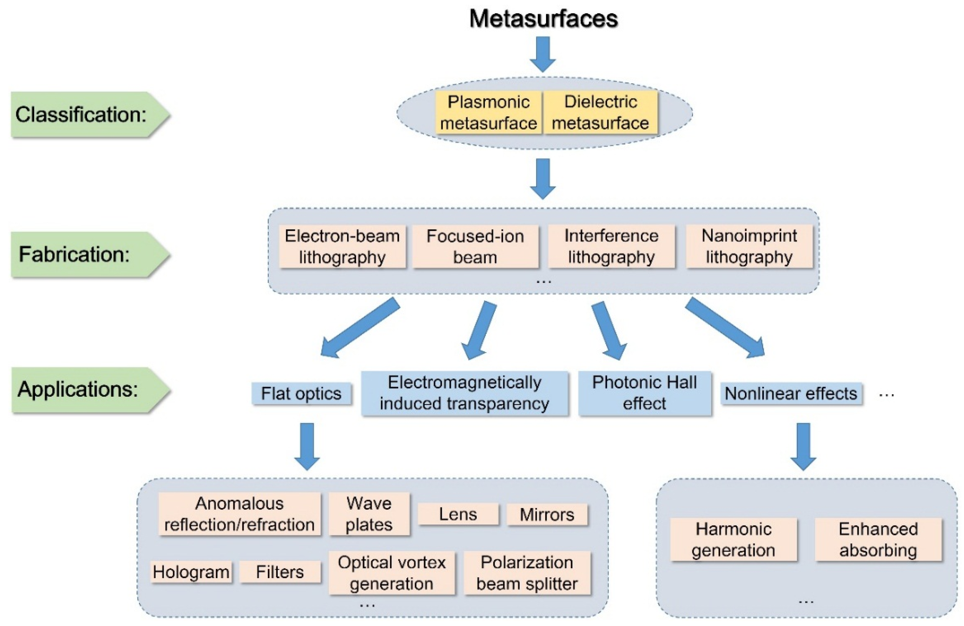
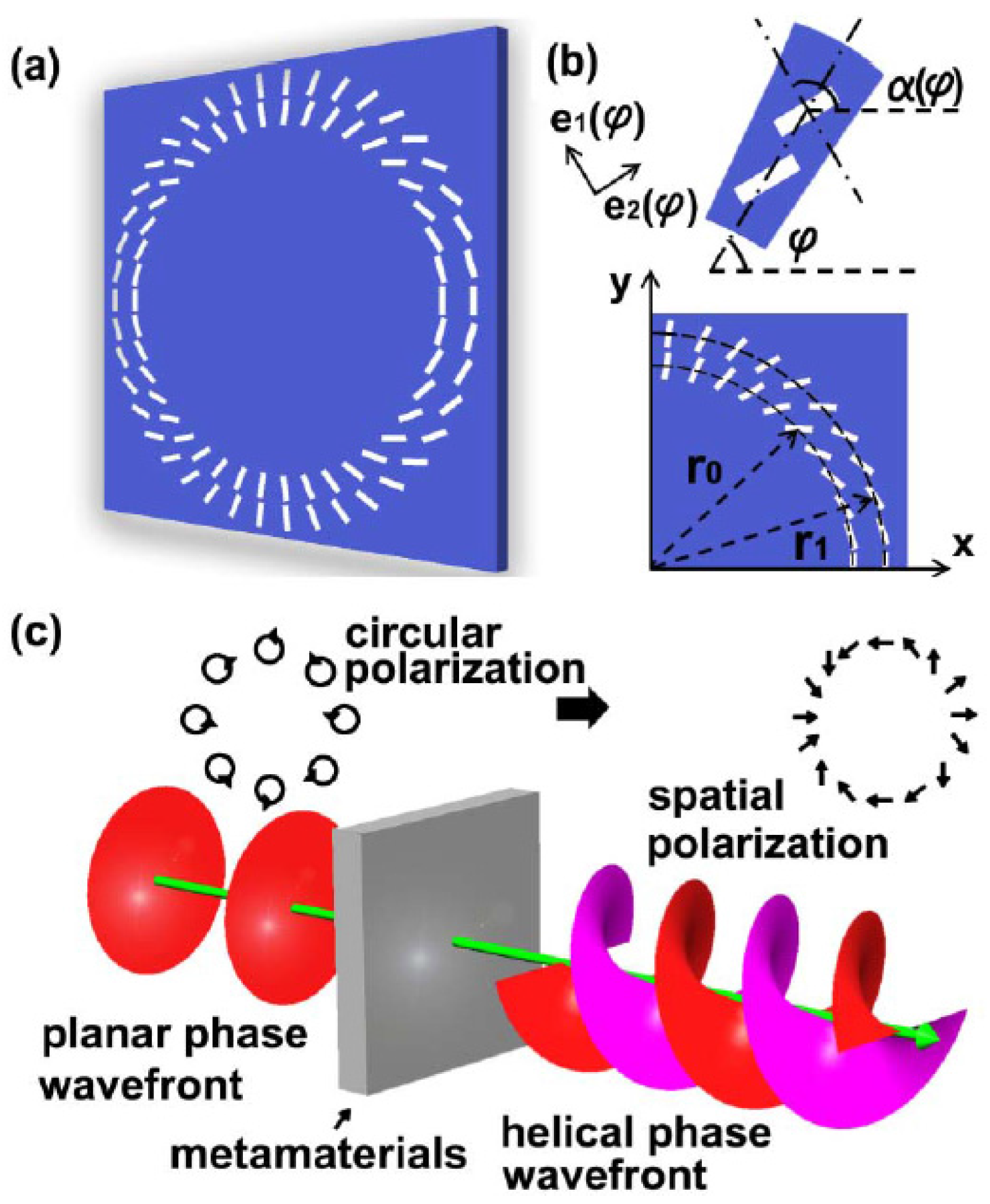
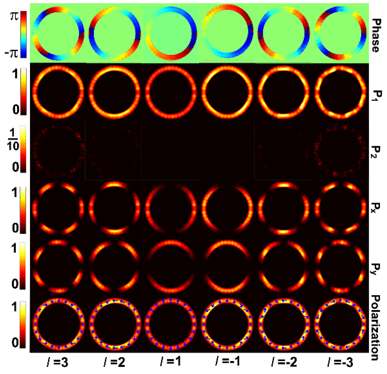
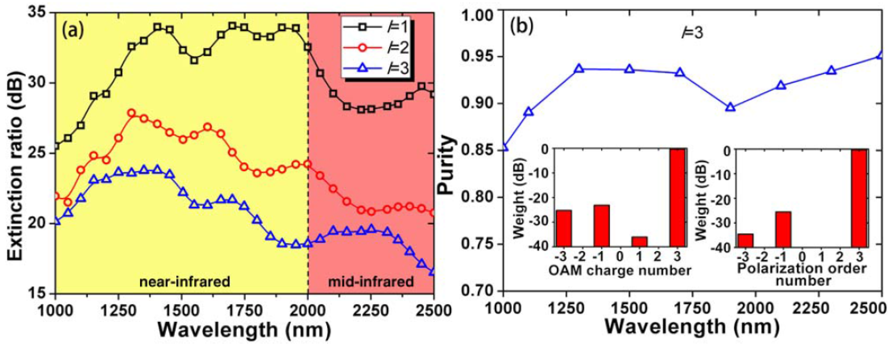
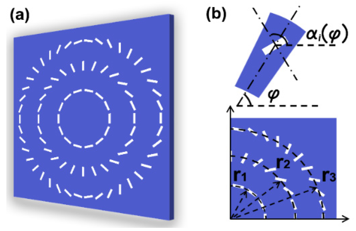
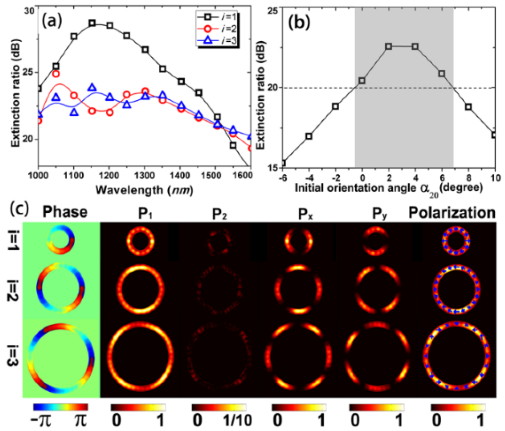
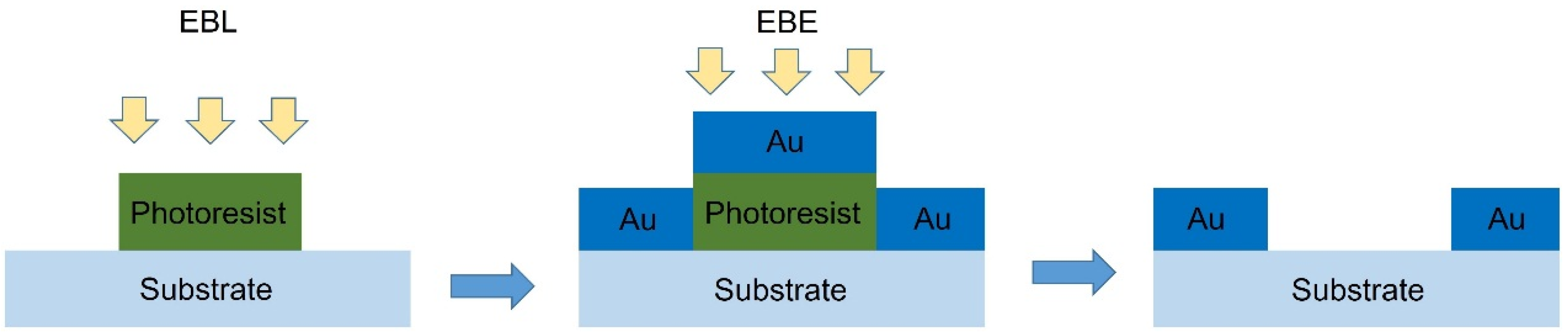
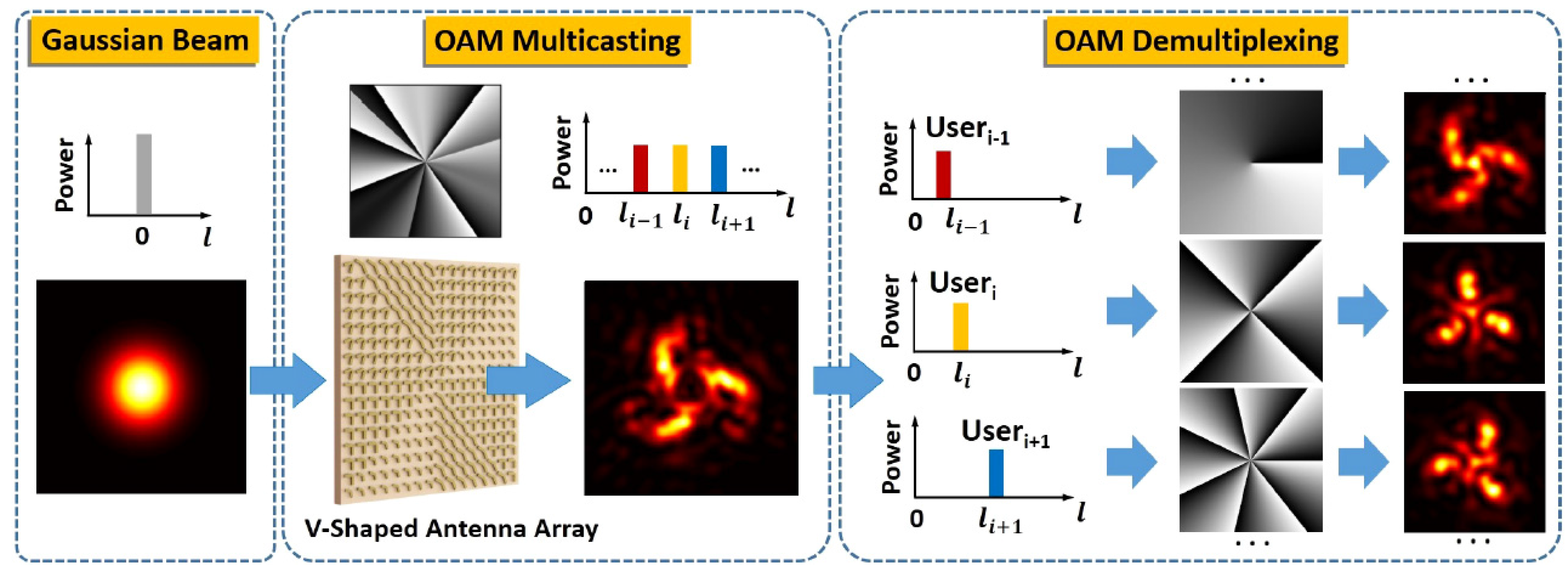
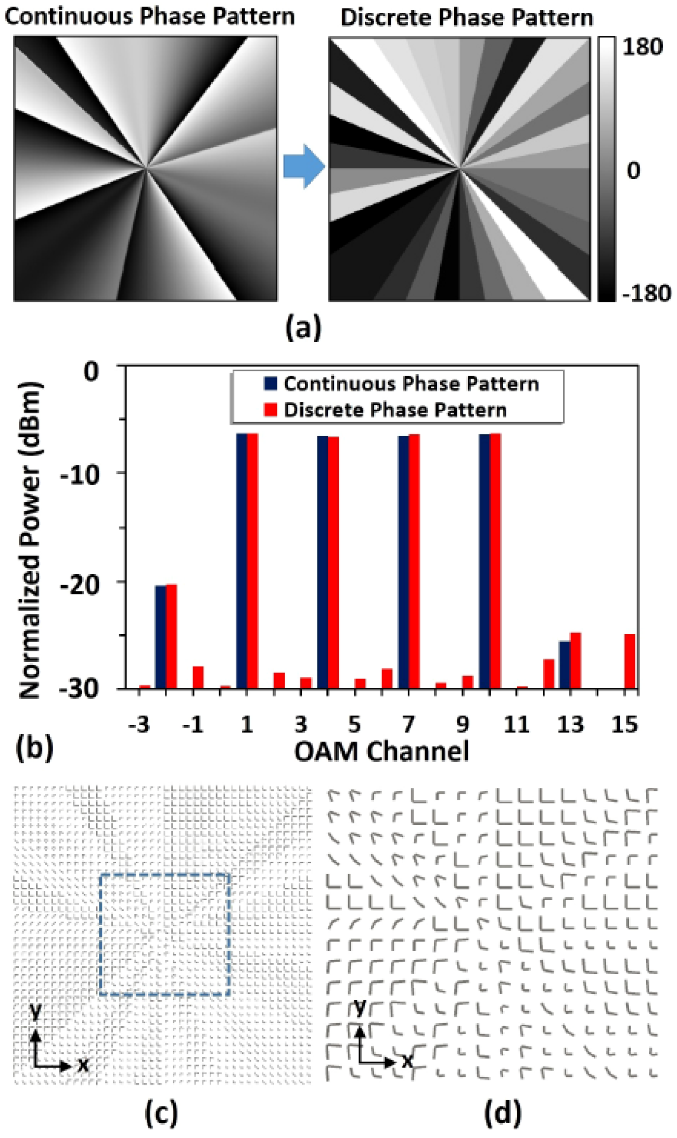
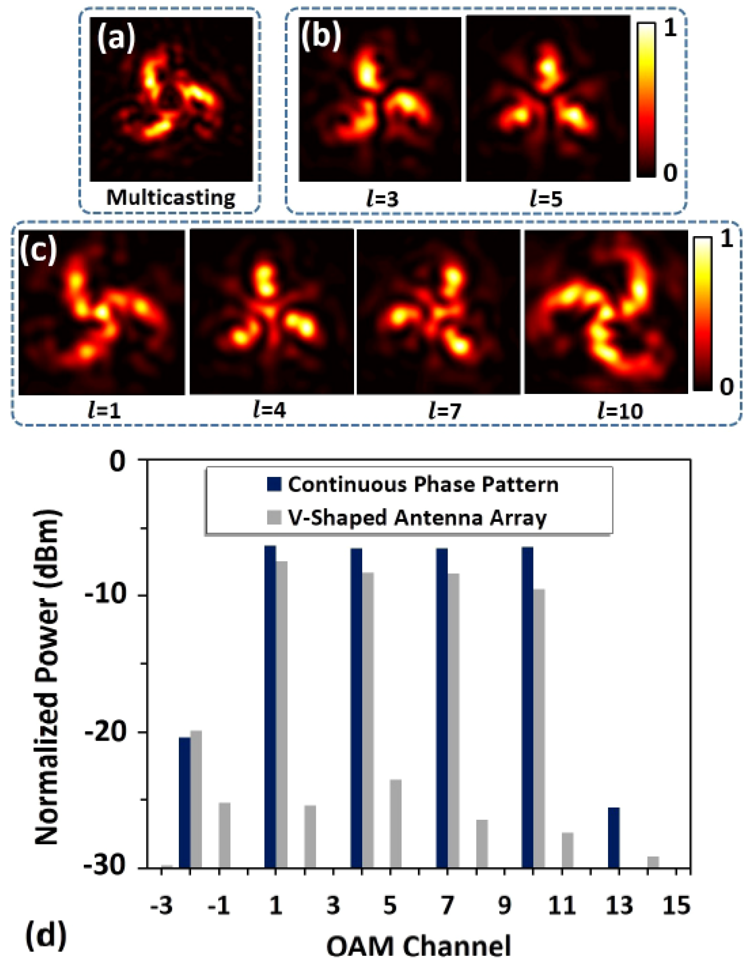
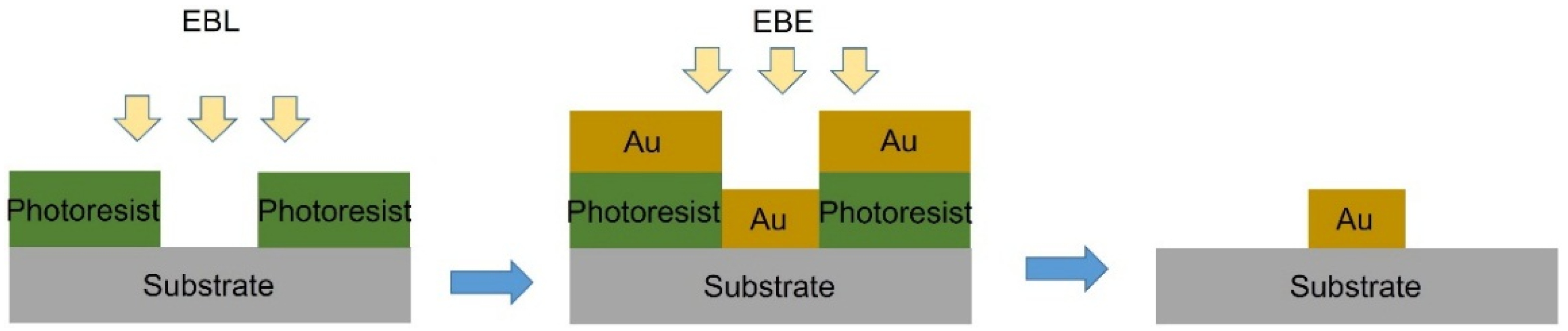
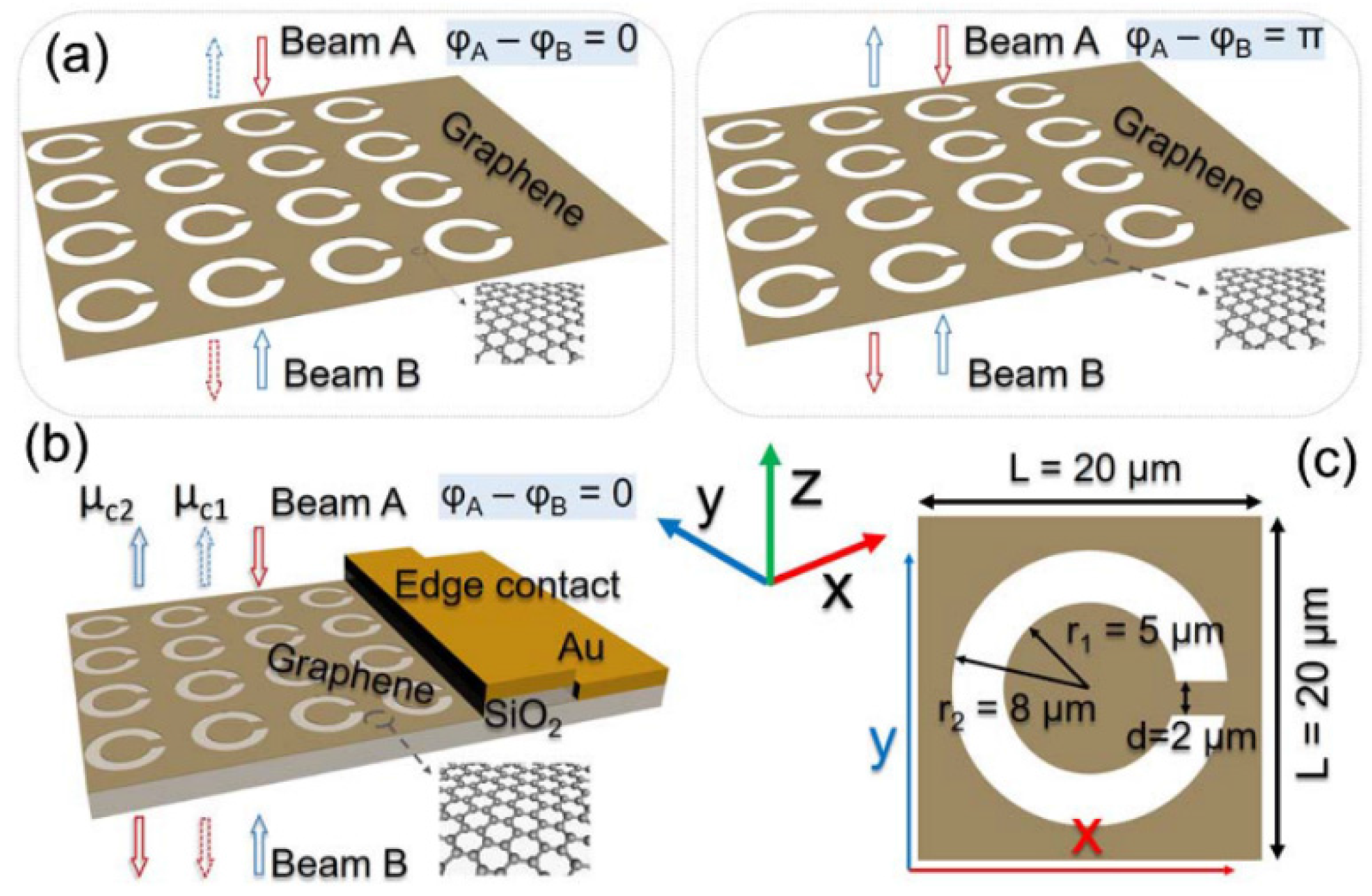
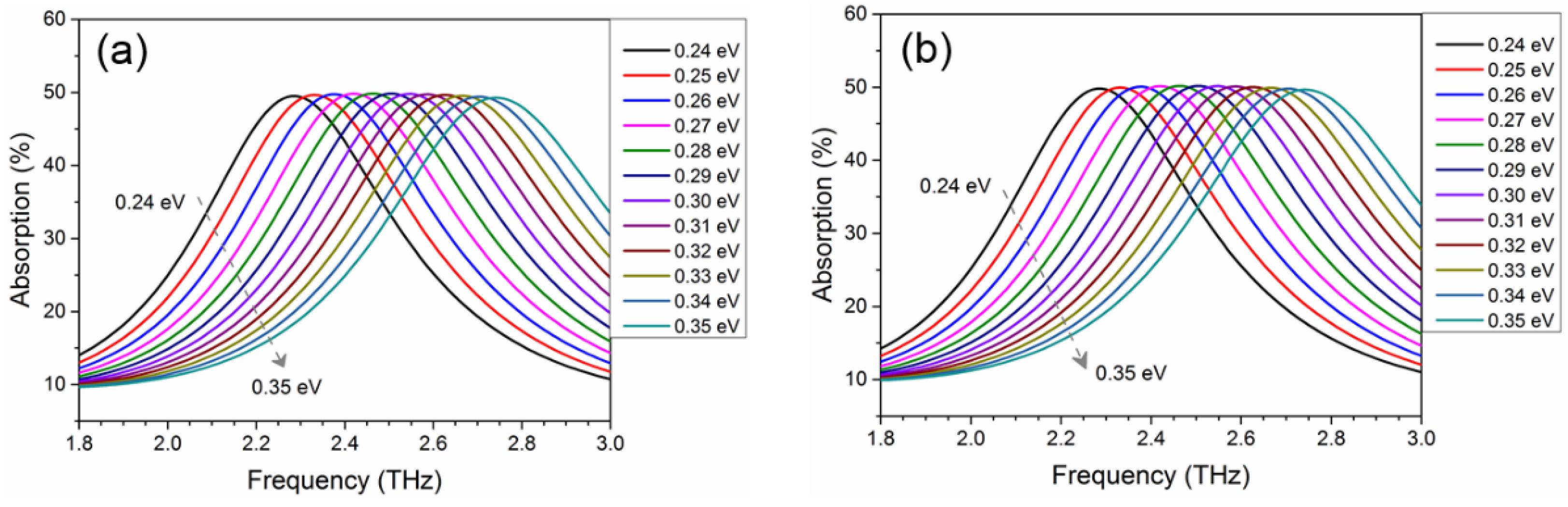
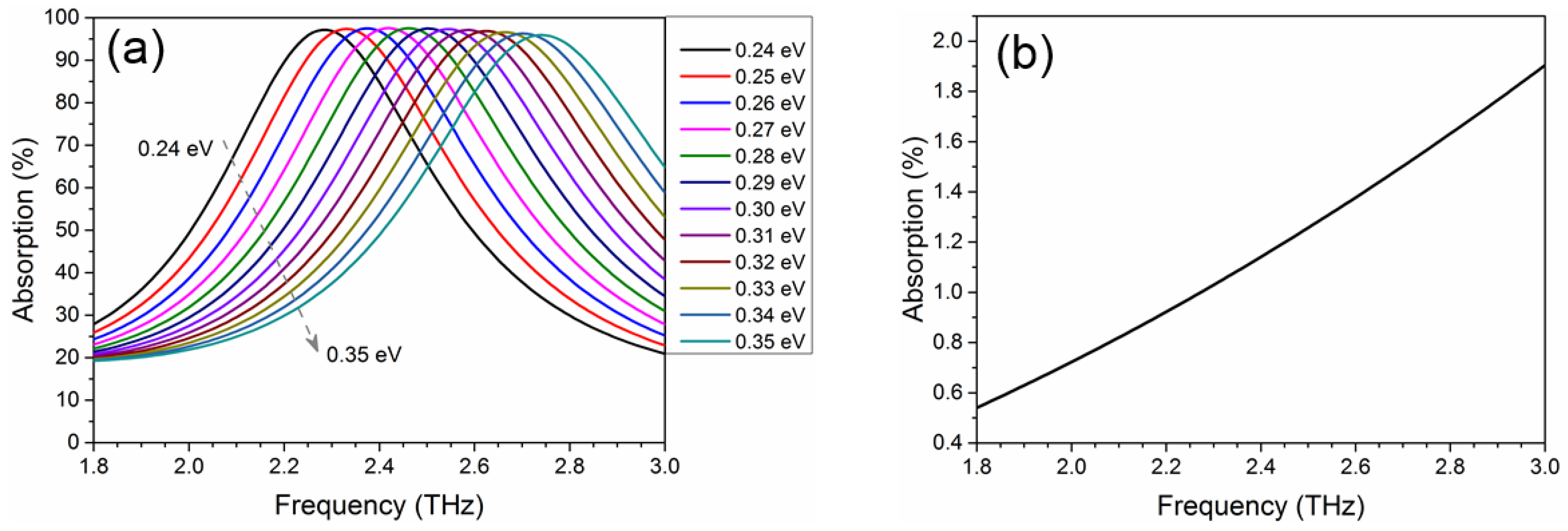
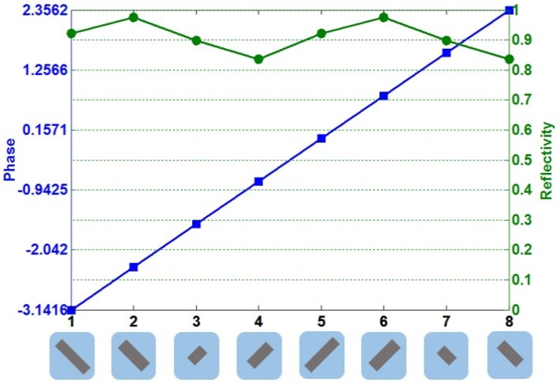
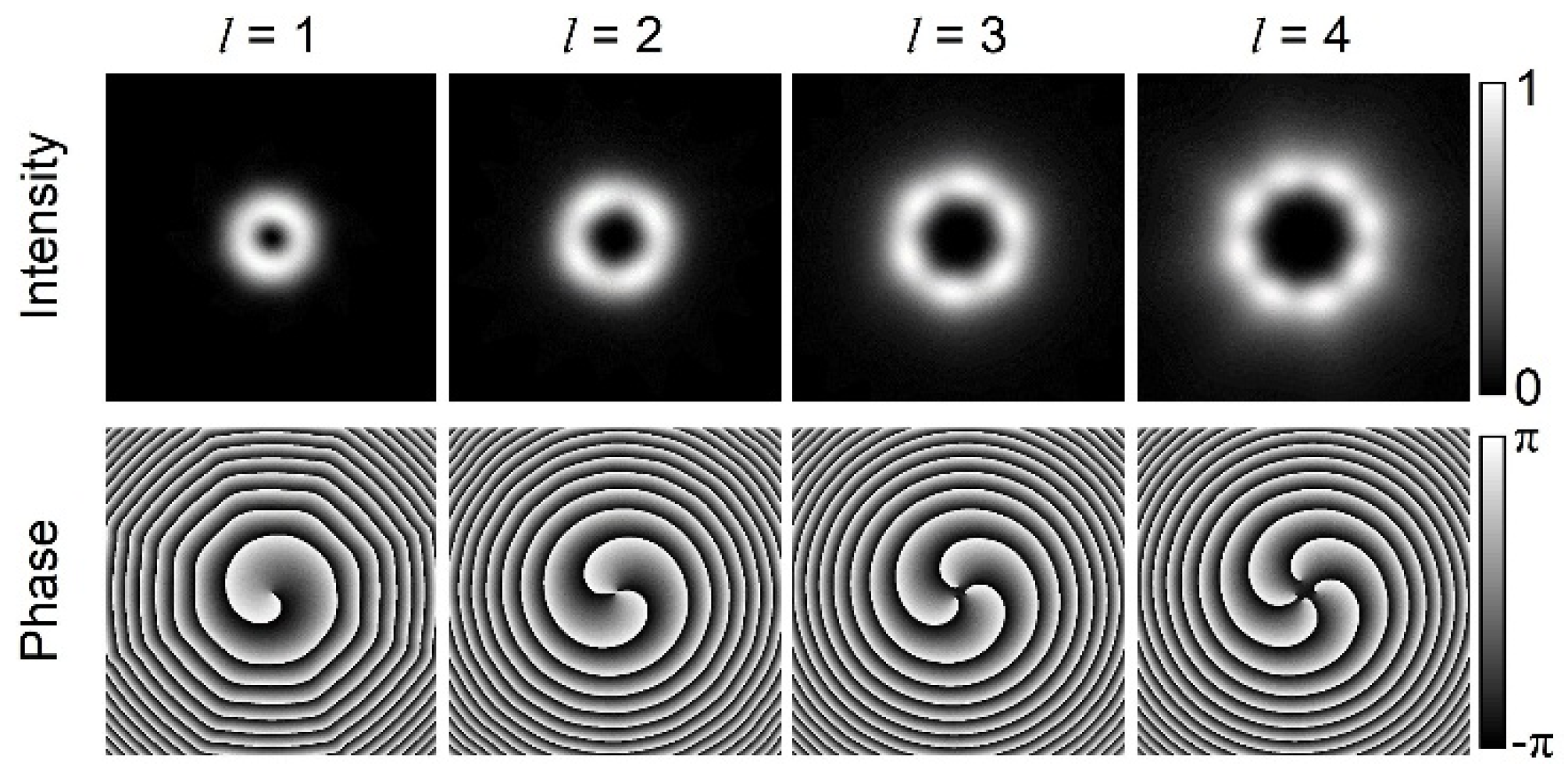
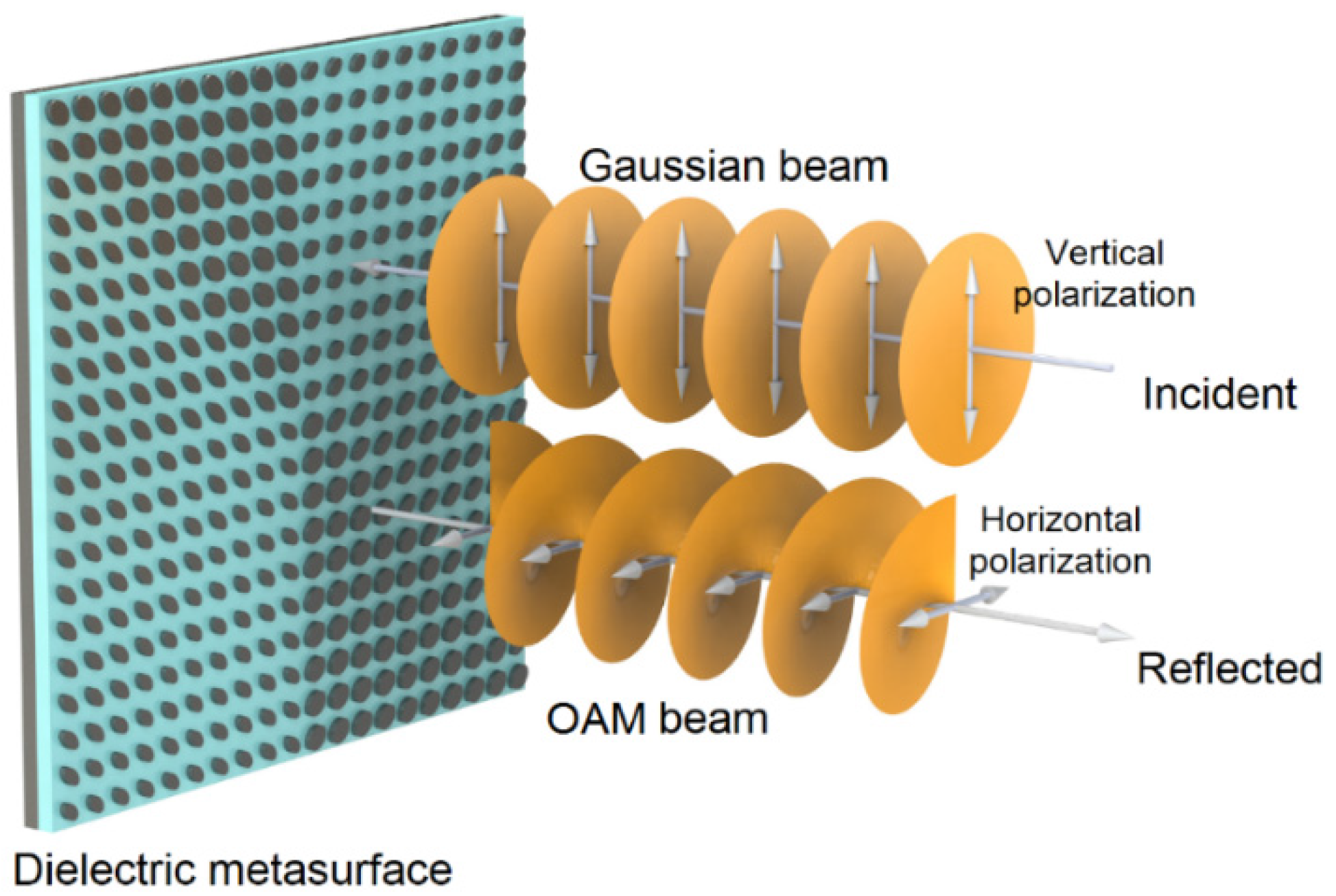
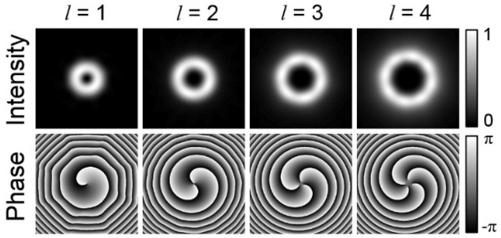
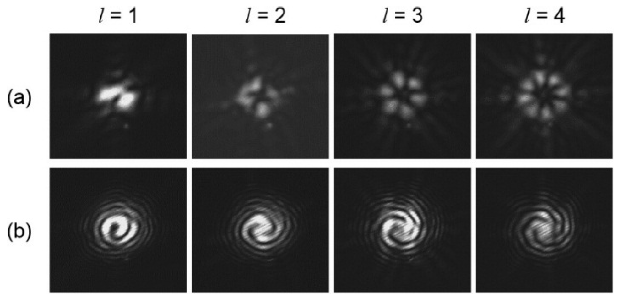
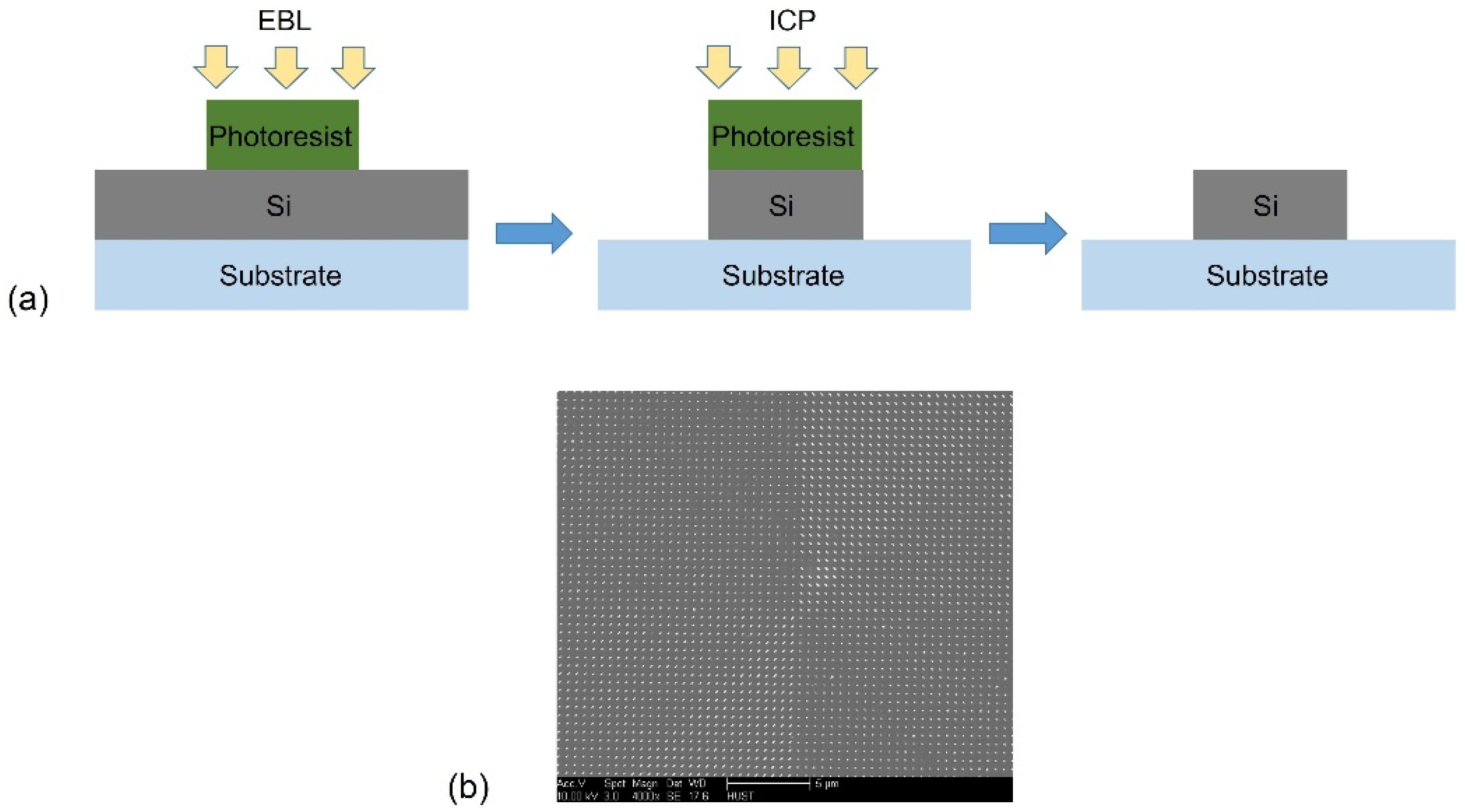
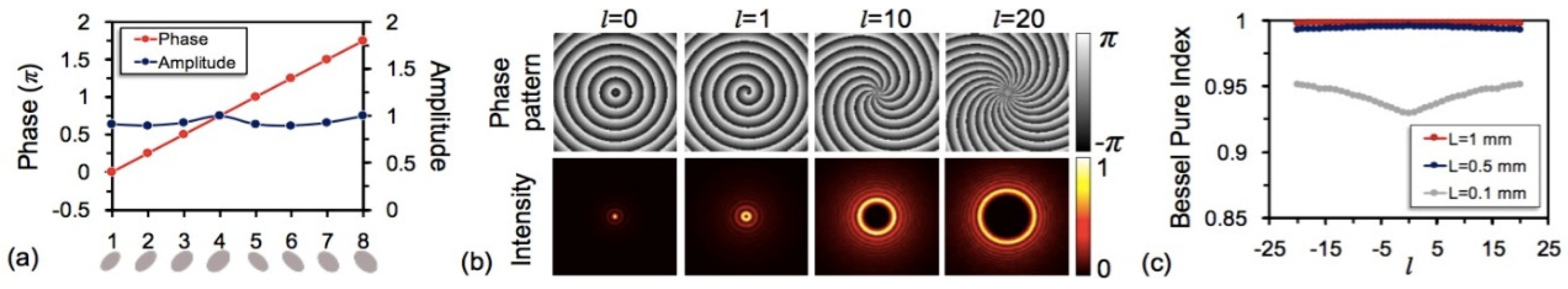
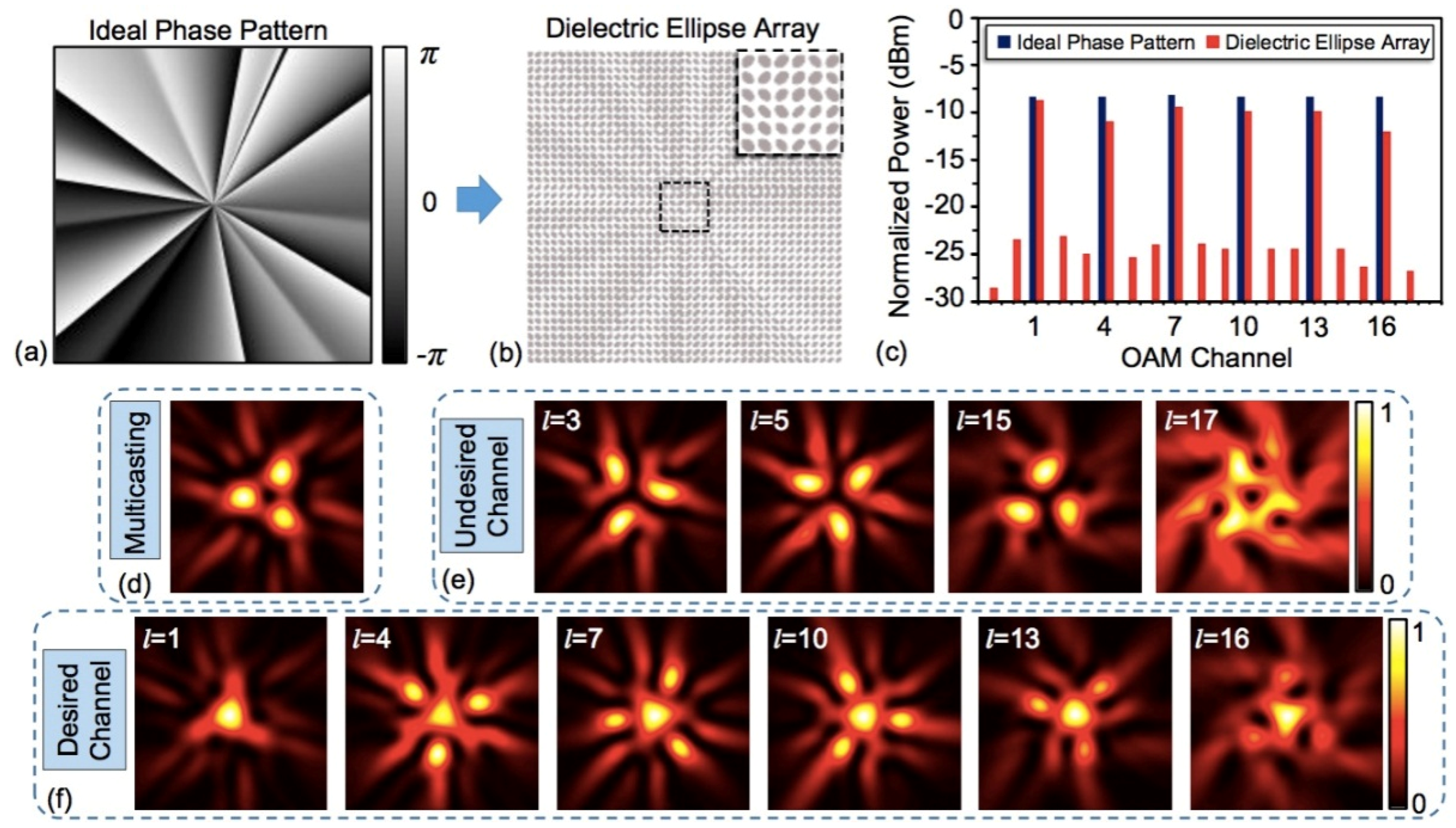
 | Metal V-shaped nano-antennas to generate optical beams carrying orbital angular momentum (OAM). Reproduced with permission from [34], Copyright The American Association for the Advancement of Science, 2011. |
 | Au patch antennas separated from a metal back plane by a MgF2 spacer to realize anomalous reflections. Reproduced with permission from [81], Copyright American Chemical Society, 2012. |
 | H-shaped microwave nano-antenna arrays to realize high efficiency conversion from propagating waves to surface waves. Reproduced with permission from [82], Copyright Nature Publishing Group, 2012. |
 | Metal nanorods to generate a hologram. Reproduced with permission from [95], Copyright Nature Publishing Group, 2013. |
 | Freestanding nanofabricated fishnet metasurface to function as a broadband band pass filter. Reproduced with permission from [96], Copyright Nature Publishing Group, 2013. |
 | Rectangular apertures arranged in an array with rotational symmetry in metal film to generate OAM beams. Reproduced with permission from [98], Copyright The Optical Society, 2012. |
 | Metal nanorods to generate broadband OAM beams. Reproduced with permission from [99], Copyright American Chemical Society, 2012. |
 | Split-ring resonators to generate the second harmonic. Reproduced with permission from [102], Copyright Nature Publishing Group, 2015. |
 | Er-doped Si-rich silicon nitride nano-pillar array for enhanced omnidirectional light extraction and OAM beam generation. Reproduced with permission from [97], Copyright AIP Publishing LLC, 2012. |
 | Si-based metasurfaces possessing sharp electromagnetically-induced transparency-like resonances in the near-infrared regime. Reproduced with permission from [111], Copyright Nature Publishing Group, 2014. |
 | Silicon nanobeams antennas function as a flat axicon to generate Bessel beams. Reproduced with permission from [85], Copyright The American Association for the Advancement of Science, 2014. |
 | Amorphous-silicon nanoridges to realize polarization beam splitting at the pixel-level. Reproduced with permission from [100], Copyright The Optical Society, 2015. |
 | Silicon nanodiscs to achieve high transmission and full phase control in visible wavelengths. Reproduced with permission from [125], Copyright John Wiley and Sons, 2015. |
 | Silicon cut-wire array in combination with a silver ground plane to achieve high linear polarization conversion efficiency in the near-infrared band. Reproduced with permission from [126], Copyright American Chemical Society, 2014. |
 | Silicon nano-pillar array to realize low loss micro-lenses in the near-infrared band. Reproduced with permission from [127], Copyright The Optical Society, 2014. |
 | Dielectric metasurface with a tailored phase gradient to achieve carpet cloaking at microwave frequencies [128] |
© 2016 by the authors; licensee MDPI, Basel, Switzerland. This article is an open access article distributed under the terms and conditions of the Creative Commons Attribution (CC-BY) license (http://creativecommons.org/licenses/by/4.0/).
Share and Cite
MDPI and ACS Style
Wang, J.; Du, J. Plasmonic and Dielectric Metasurfaces: Design, Fabrication and Applications. Appl. Sci. 2016, 6, 239. https://doi.org/10.3390/app6090239
AMA Style
Wang J, Du J. Plasmonic and Dielectric Metasurfaces: Design, Fabrication and Applications. Applied Sciences. 2016; 6(9):239. https://doi.org/10.3390/app6090239
Chicago/Turabian StyleWang, Jian, and Jing Du. 2016. "Plasmonic and Dielectric Metasurfaces: Design, Fabrication and Applications" Applied Sciences 6, no. 9: 239. https://doi.org/10.3390/app6090239
Note that from the first issue of 2016, this journal uses article numbers instead of page numbers. See further details here.