
Switched 4-to-1 Transimpedance Combining Amplifier for Receiver Front-End Circuit of Static Unitary Detector-Based LADAR System


Abstract
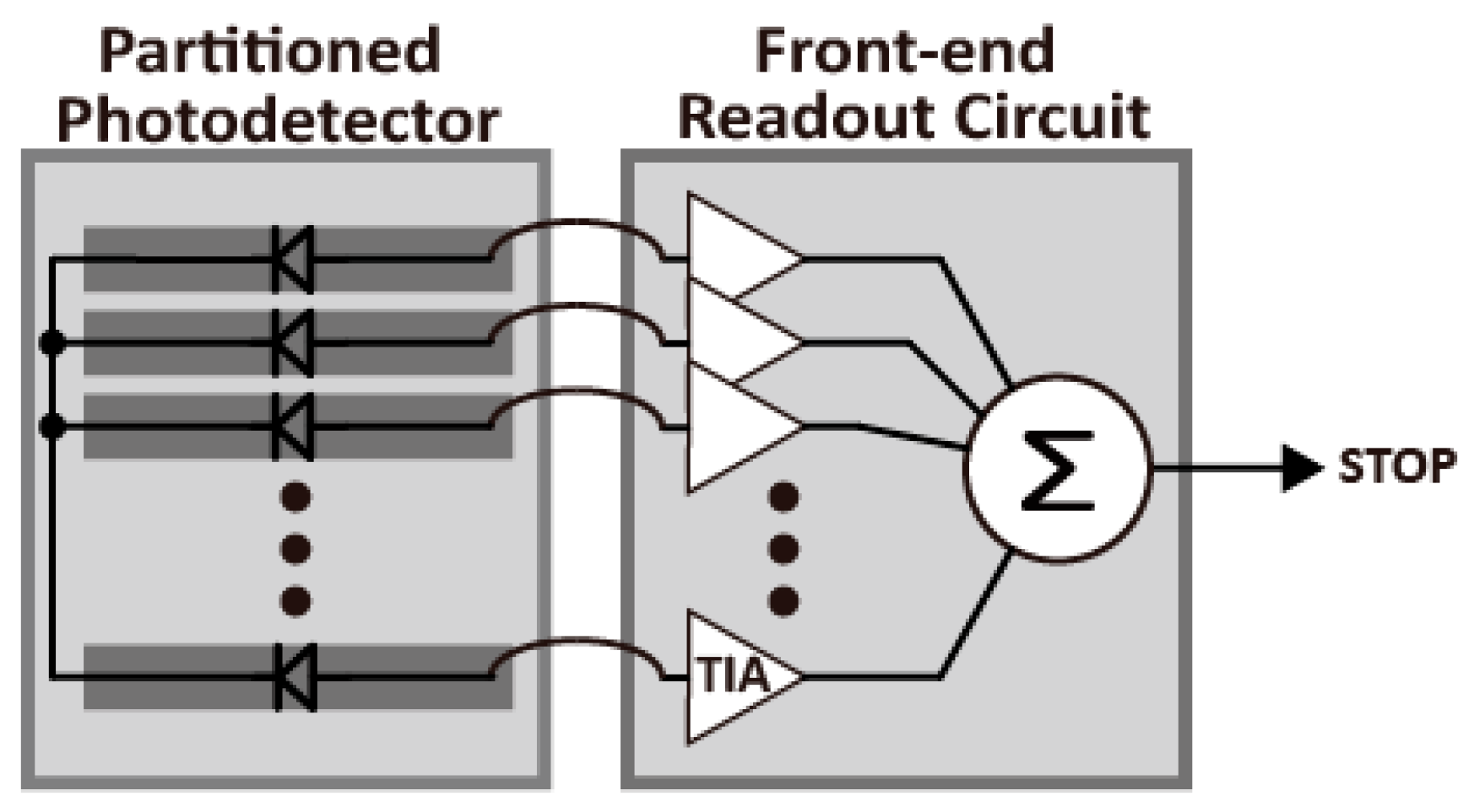
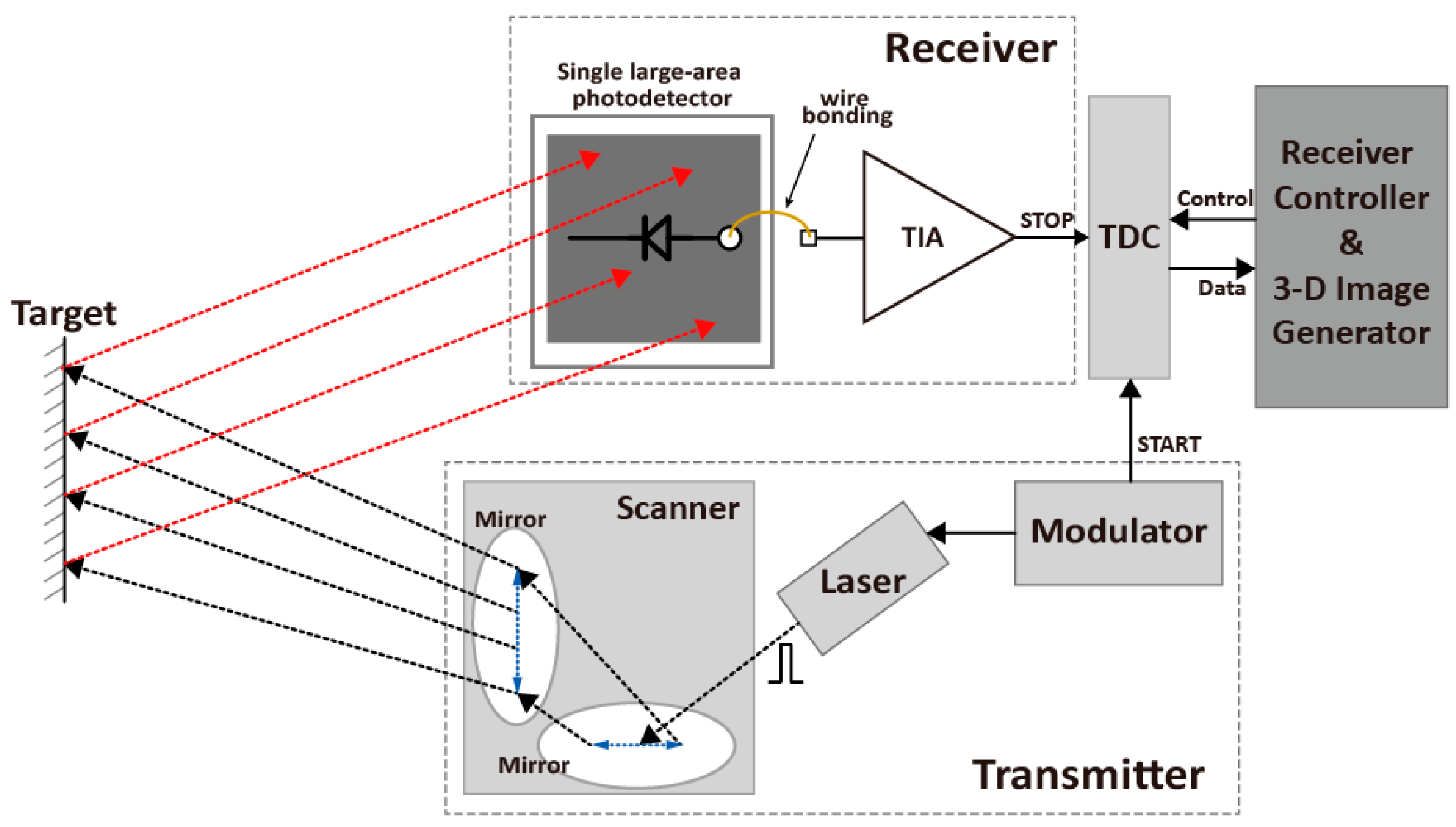
:1. Introduction
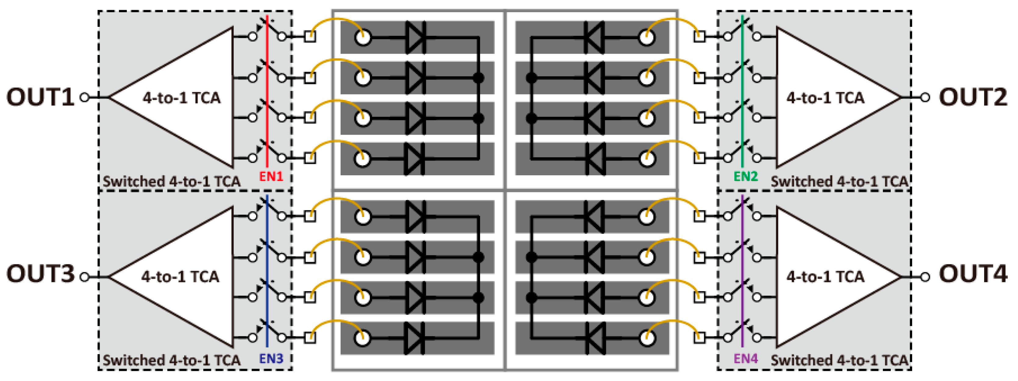
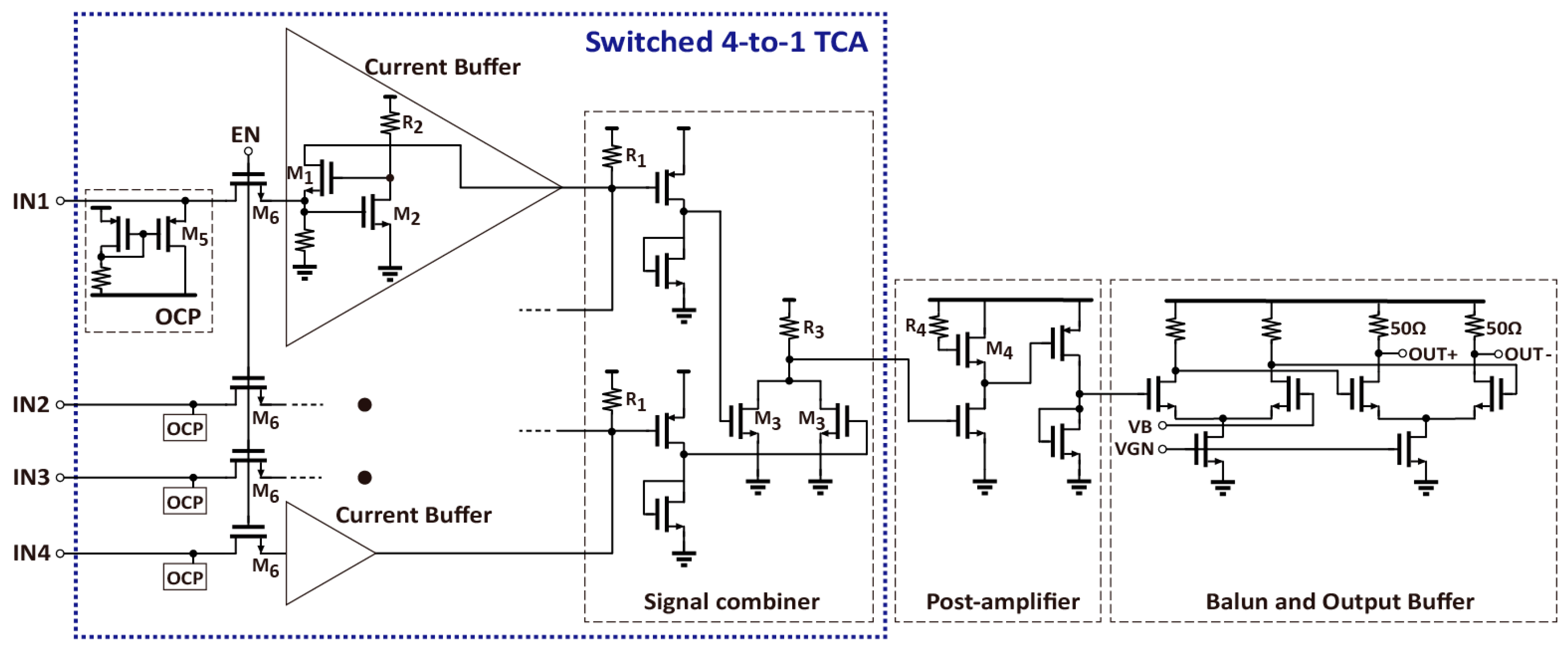
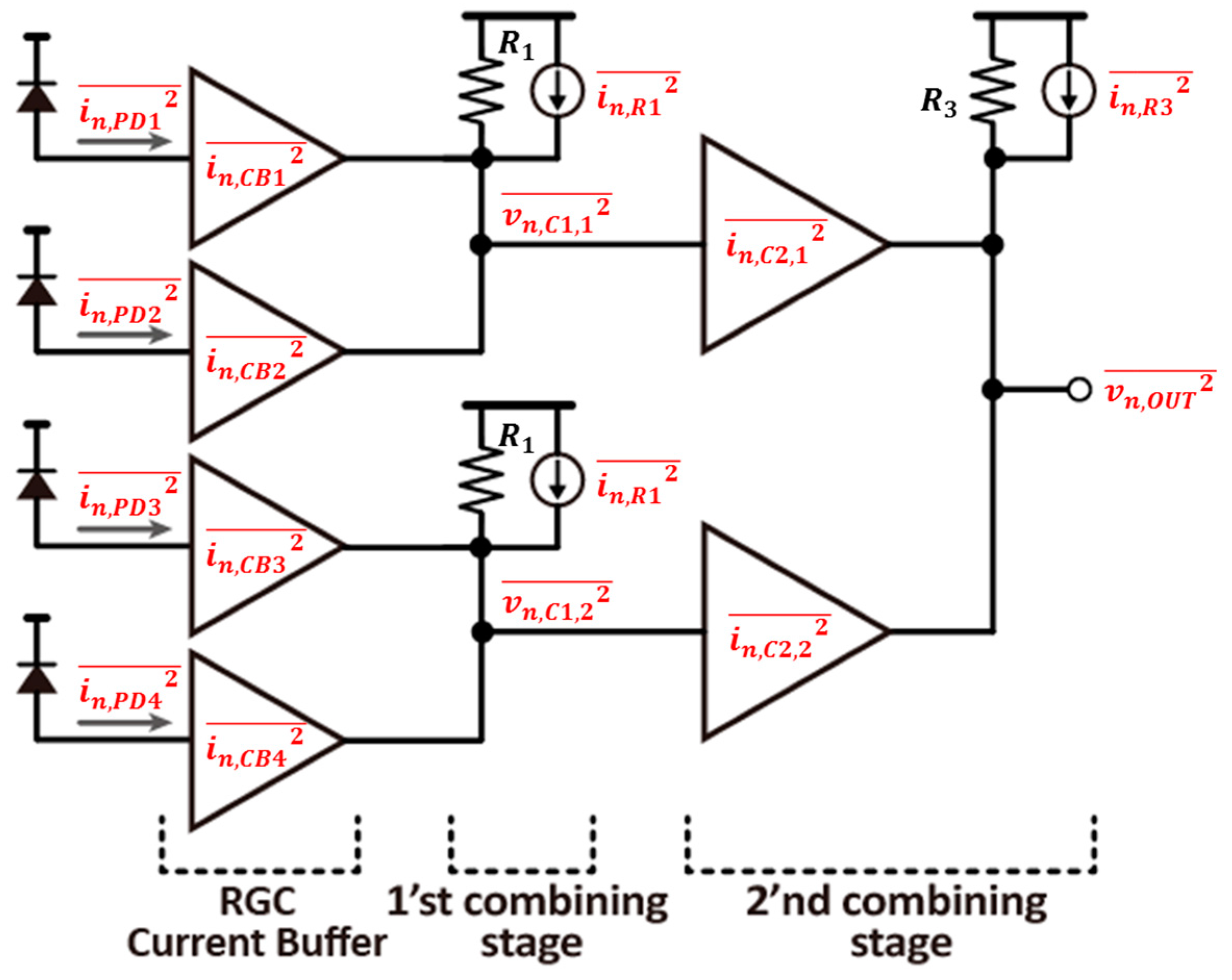
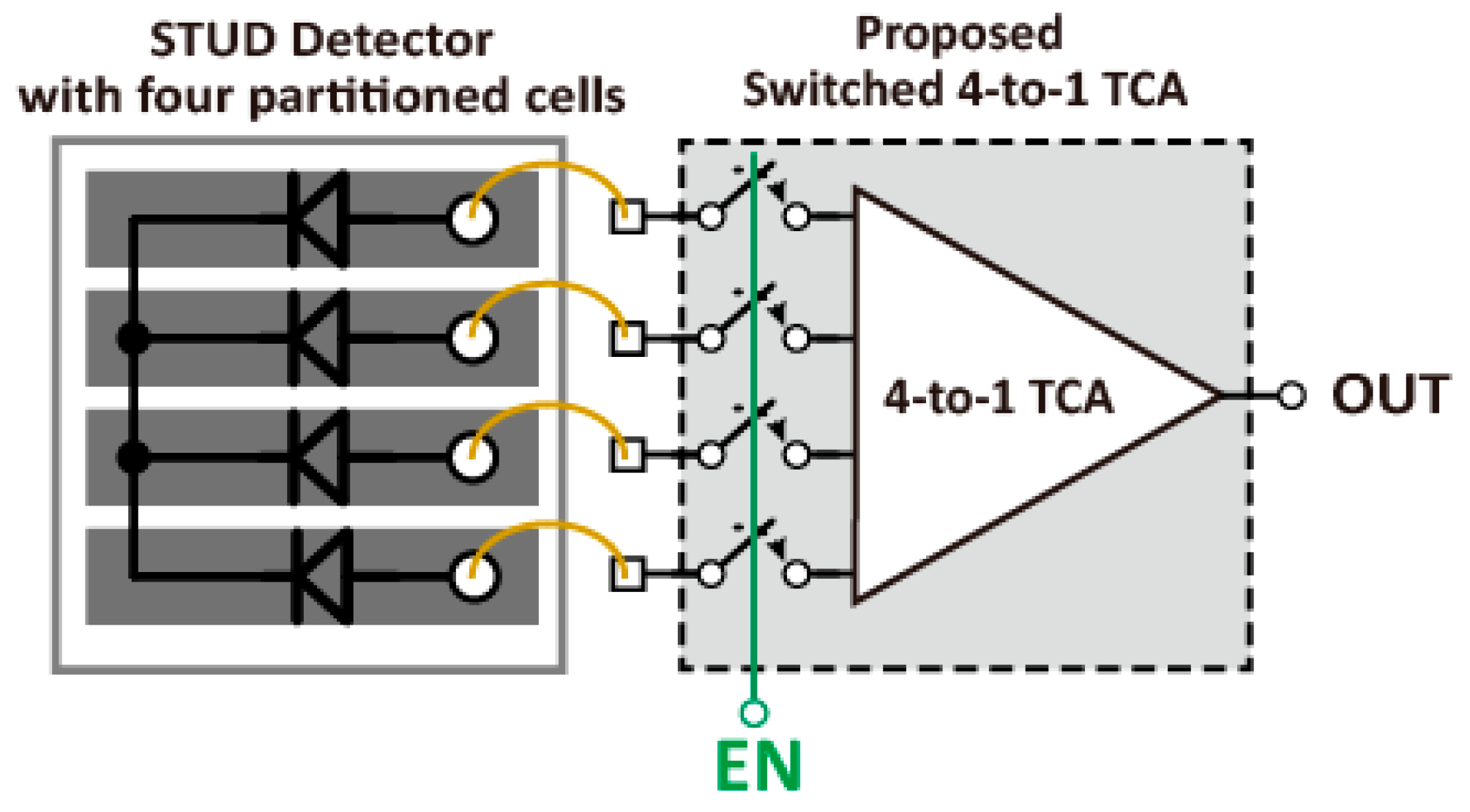
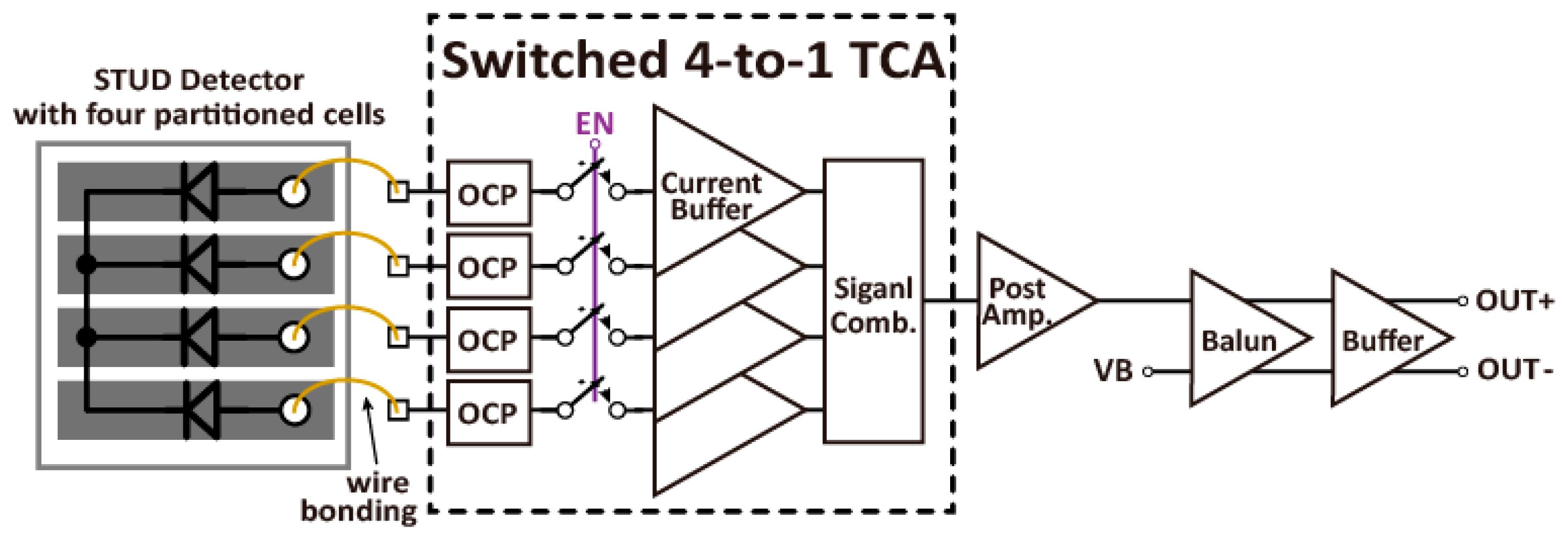
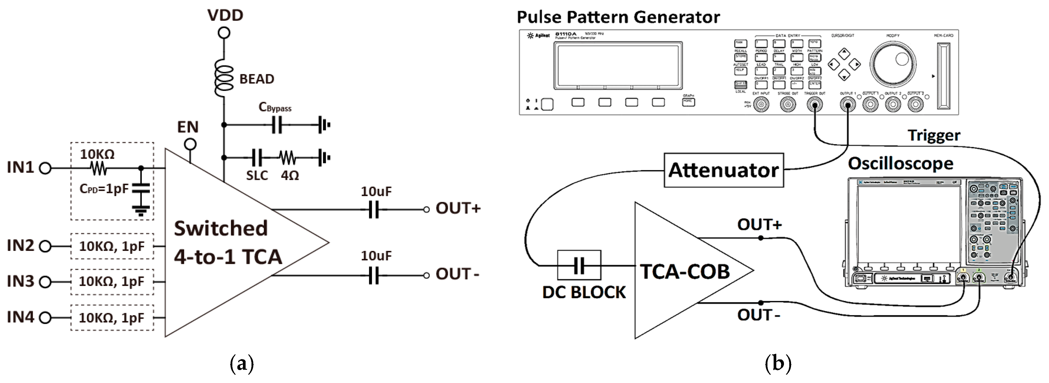
2. Architecture Description
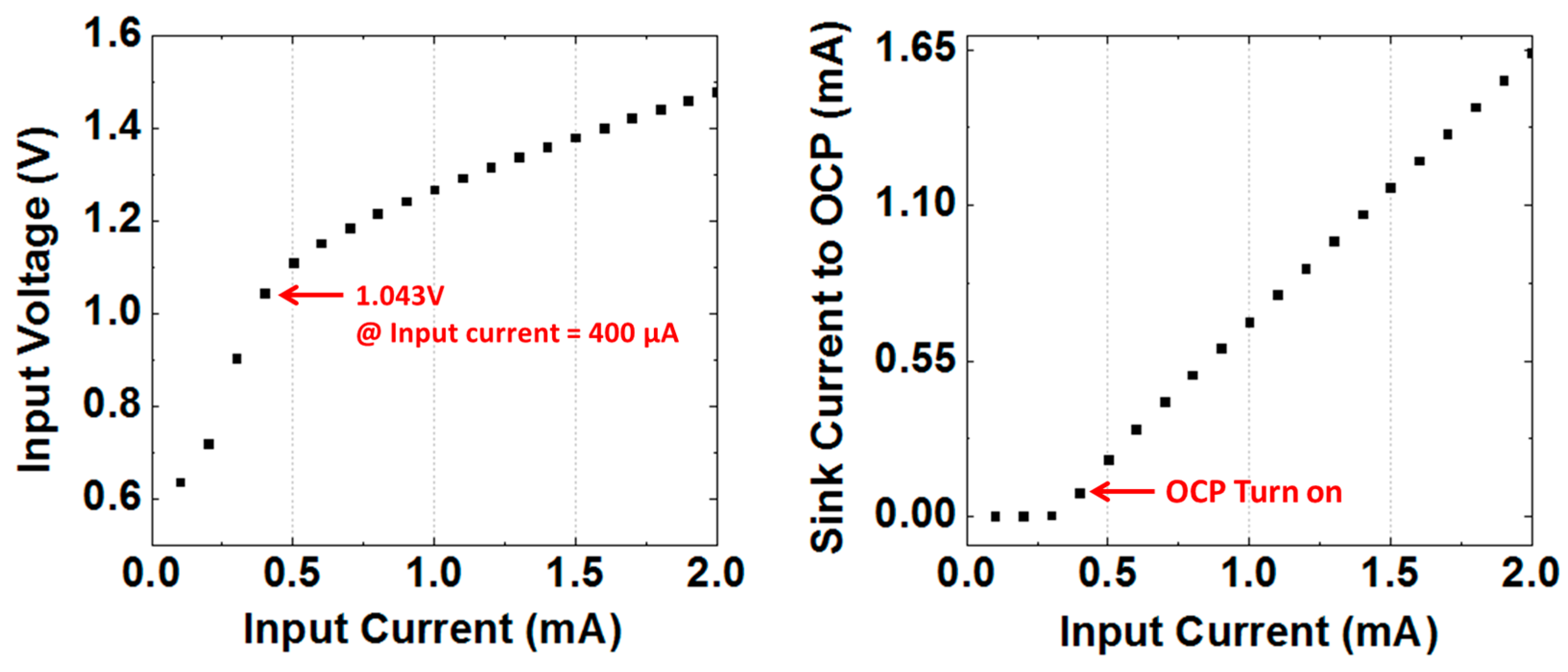
2.1. OCP and Input Switch
2.2. 4-to-1 TCA, Post-Amplifier, Balun, and Output Buffer
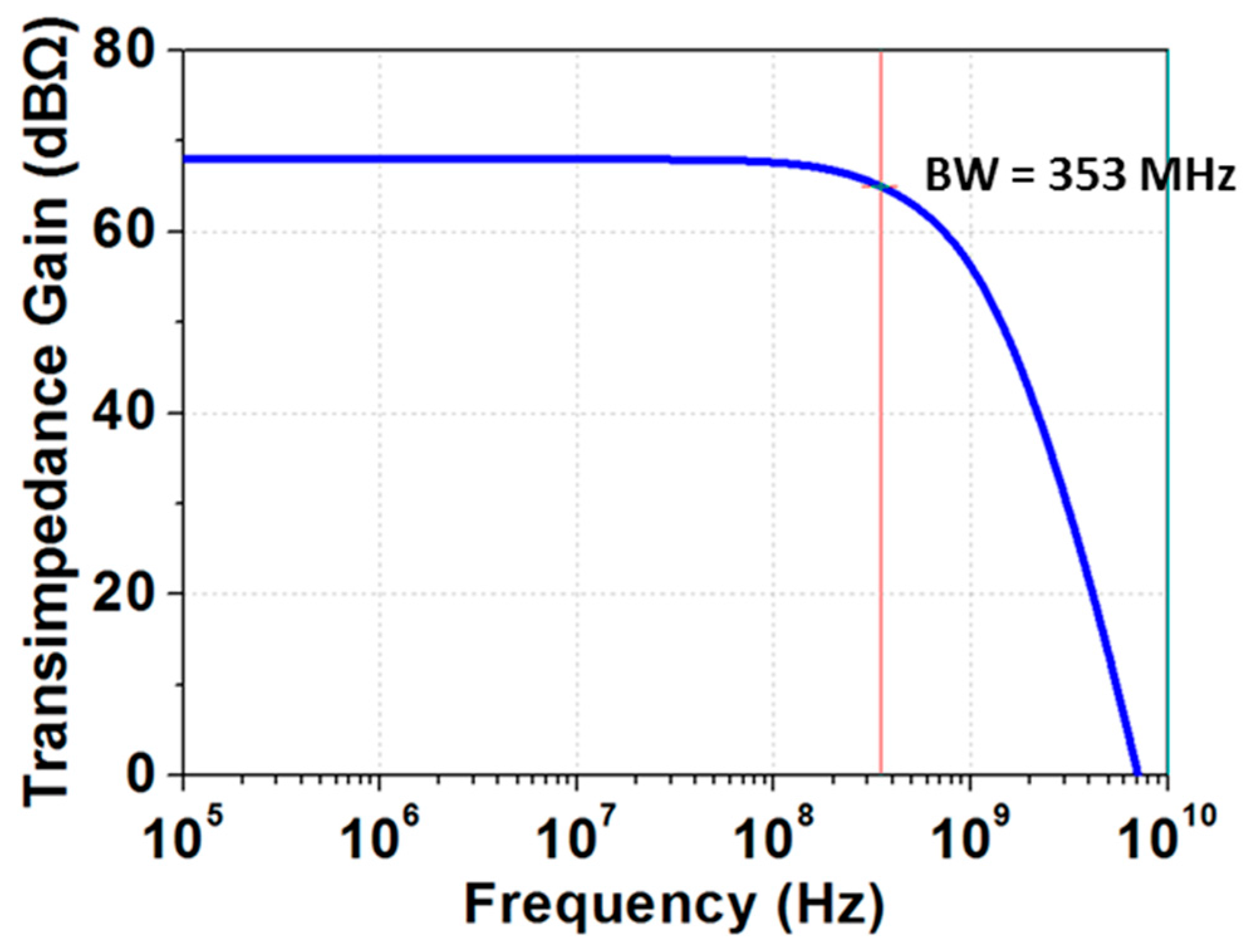
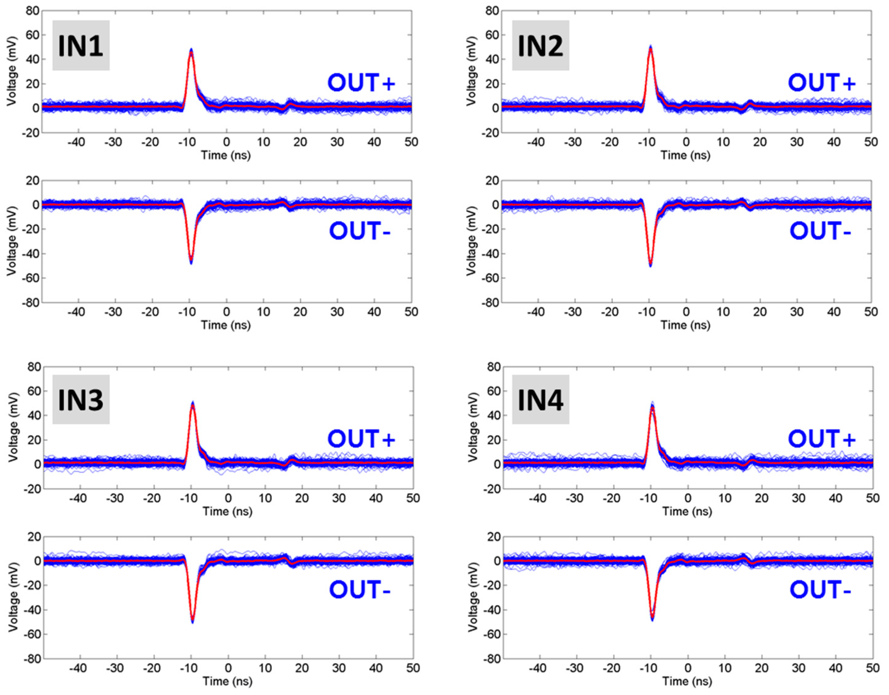
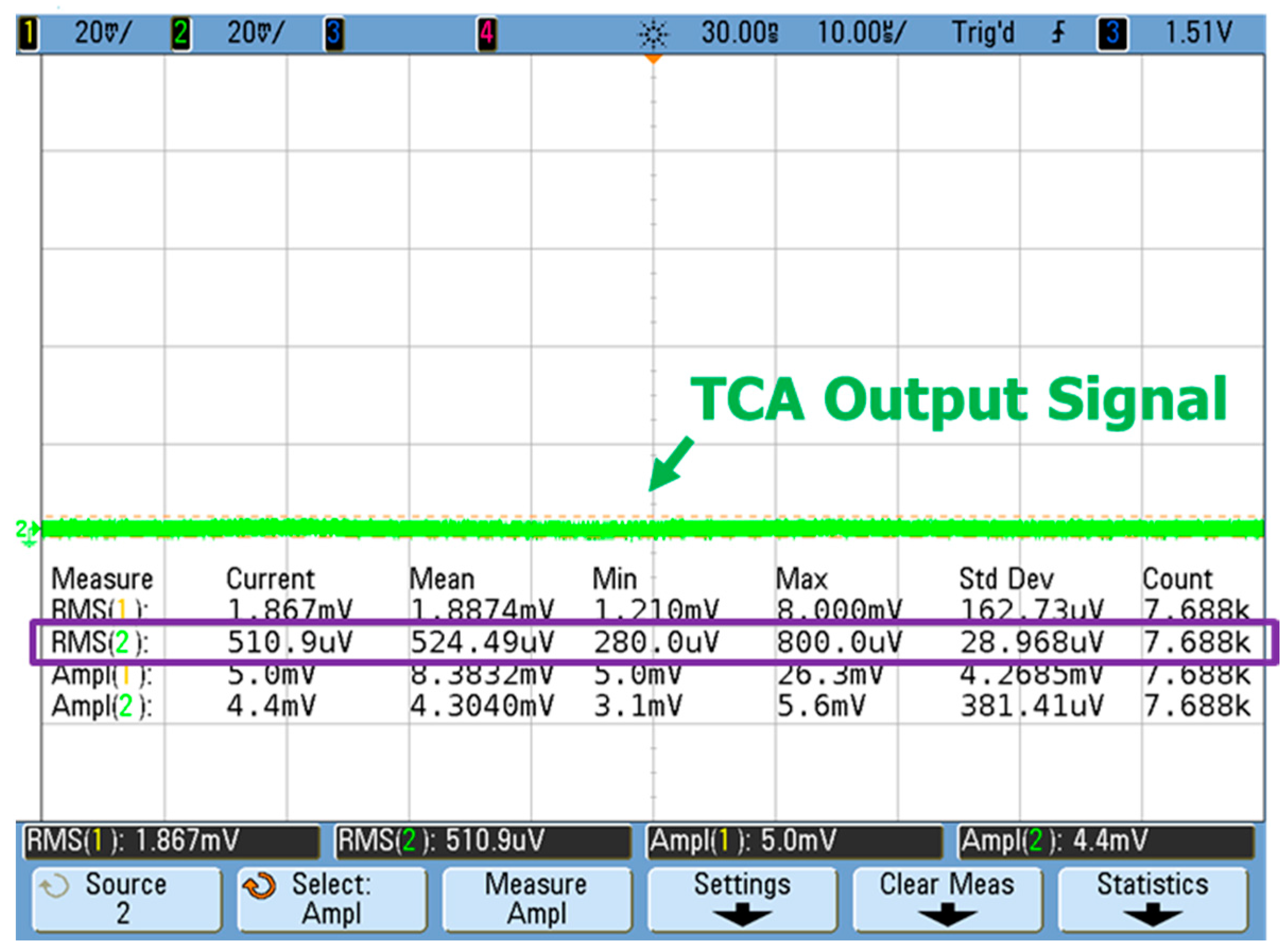
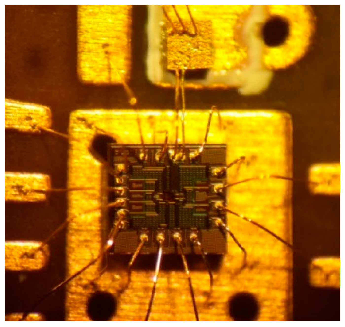
3. Measurement Results
4. Conclusions
Acknowledgments
Author Contributions
Conflicts of Interest
References
- Thrun, S.; Montemerlo, M.; Dahlkamp, H.; Stavens, D.; Aron, A.; Diebel, J.; Fong, P.; Gale, J.; Halpenny, M.; Hoffmann, G.; et al. Stanley: The robot that won the DARPA grand challenge. J. Field Robot. 2006, 23, 661–692. [Google Scholar] [CrossRef]
- Kaisto, I.; Kostamovaara, J.; Moring, I.; Myllyla, R. Laser rangefinding techniques in sensing of 3D objects. Proceedings of SPIE—Sensing and Reconstruction of Three-Dimensional Objects and Scenes, Santa Clara, CA, USA, 1 January 1990; SPIE: Bellingham, WA, USA, 1990; Volume 1260, pp. 122–133. [Google Scholar]
- Hollaus, M.; Wagner, W.; Maier, B.; Schadauer, K. Airborne laser scanning of forest stem volume in a mountainous environment. Sensors 2007, 7, 1559–1577. [Google Scholar] [CrossRef]
- Buller, G.; Wallace, A. Ranging and three-dimensional imaging using time-correlated single-photon counting and point-by-point acquisition. IEEE J. Sel. Top. Quantum Electron. 2007, 13, 1006–1015. [Google Scholar] [CrossRef]
- Dorninger, P.; Pfeifer, N. A comprehensive automated 3D approach for building extraction, reconstruction, and regularization from airborne laser scanning point clouds. Sensors 2008, 8, 7323–7343. [Google Scholar] [CrossRef] [PubMed]
- Wang, C.; Glenn, N.F. Integrating LIDAR intensity and elevation data for terrain characterization in a forested area. IEEE Geosci. Remote Sens. Lett. 2009, 6, 463–466. [Google Scholar] [CrossRef]
- Amzajerdian, F.; Gao, C.-Q.; Xie, T.-Y. 3D imaging LADAR with linear array devices: Laser, detector and ROIC. Proceedings of SPIE—International Symposium on Photoelectronic Detection and Imaging 2009: Laser Sensing and Imaging, Beijing, China, 17 June 2009; SPIE: Bellingham, WA, USA, 2009; Volume 7382, p. 738209. [Google Scholar]
- Kurtti, S.; Kostamovaara, J. An integrated laser radar receiver channel utilizing a time-domain walk error compensation scheme. IEEE Trans. Instrum. Meas. 2011, 60, 146–157. [Google Scholar] [CrossRef]
- Kang, Y.; Roh, C.; Suh, S.B.; Song, B. A Lidar-Based Decision-Making Method for Road Boundary Detection Using Multiple Kalman Filters. IEEE Trans. Ind. Electron. 2012, 59, 432–4368. [Google Scholar] [CrossRef]
- Chen, J.; Zhao, P.; Liang, H.; Mei, T. Motion Planning for Autonomous vehicle Based on Radial Basis Function Neural in Unstructured Environment. Sensors 2014, 14, 17548–17566. [Google Scholar] [CrossRef] [PubMed]
- Mheen, B.; Shim, J.-S.; Oh, M.S.; Song, J.; Song, M.; Choi, G.D.; Seo, H.; Kwon, Y.-H. High-resolution three-dimensional laser radar with static unitary detector. Electron. Lett. 2014, 50, 313–315. [Google Scholar] [CrossRef]
- Glennie, C.; Lichti, D.D. Static calibration and analysis of the velodyne HDL-64E S2 for high accuracy mobile scanning. Remote Sens. 2010, 2, 1610–1624. [Google Scholar] [CrossRef]
- Stettner, R.; Bailey, H.; Silverman, S. Three dimensional Flash LADAR focal planes and time dependent imaging. Int. J. High Speed Electron. Syst., 2008, 18, 401–406. [Google Scholar] [CrossRef]
- Lee, E.G.; An, J.; Kim, C.Y. A fully integrated four-input combining receiver front-end circuit for laser radar with static unitary detector. Electron. Lett. 2014, 50, 1543–1545. [Google Scholar] [CrossRef]
- Lee, E.G.; Lee, J.E.; Song, M.; Choi, G.D.; Mheen, B.; Jung, B.C.; Kim, C.Y. 4-to-1 Transimpedance Combining Amplifier-Based Static Unitary Detector for High-Resolution of LADAR Sensor. Analog Integr. Circuits Signal Process. 2016. submitted. [Google Scholar]
- Ngo, T.-H.; Kim, C.-H.; Kwon, Y.J.; Ko, J.S.; Kim, D.-B.; Park, H.-H. Wideband receiver for a three-dimensional ranging LADAR system. IEEE Trans. Circuits Syst. I Regul. Pap. 2013, 60, 448–456. [Google Scholar] [CrossRef]
- Park, S.M.; Yoo, H. 1.25-Gb/s regulated cascode CMOS transimpedance amplifier for gigabit ethernet applications. IEEE J. Solid-State Circuits 2004, 39, 112–121. [Google Scholar] [CrossRef]
- Lee, T.H. The Design of CMOS Radio-Frequency Integrated Circuits, 2nd ed.; Cambridge University Press: Cambridge, UK, 2003. [Google Scholar]
- Ziemer, R.; Tranter, W. Principles of Communications, 2nd ed.; Houghton Mifflin: Boston, MA, USA, 1985. [Google Scholar]
- Ruotsalainen, T.; Palojärvi, P.; Kostamovaara, J. A wide dynamic range receiver channel for a pulsed time-of-flight laser radar. IEEE J. Solid-State Circuits 2001, 36, 1228–1238. [Google Scholar] [CrossRef]
- Weiner, J.S.; Lee, J.S.; Leven, A.; Baeyens, Y.; Houtsma, V.; Georgiou, G.; Yang, Y.; Frackoviak, J.; Tate, A.; Reyes, R.; et al. An InGaAs-InP HBT differential transimpedance amplifier with 47-GHz bandwidth. IEEE J. Solid-State Circuits 2004, 39, 1720–1723. [Google Scholar] [CrossRef]
- Li, C.; Palermo, S. A low-power 26-GHz transformer-based regulated cascode SiGe BiCMOS transimpedance amplifier. IEEE J. Solid-State Circuits 2013, 48, 1264–1275. [Google Scholar] [CrossRef]


| Stage | Gain | Bandwidth | Direct Current (DC) |
|---|---|---|---|
| Current buffers and first combining stages (R1) | 70 dBΩ (3 kΩ) | 330 MHz | 1.48 mA |
| Second combining stage | 2 dB | 310 MHz | 0.65 mA |
| Post-amplifier | 6 dB | 415 MHz | 2.06 mA |
| Balun and output buffer | −10 dB | 353 MHz | 3.78 mA |
| Parameter | Performance |
|---|---|
| Combining Channel | 4 |
| CPD/cell (pF) | 1 |
| Effective total CPD (pF) | 4 |
| Transimpedance gain (dBΩ) | 67.5 |
| Bandwidth (MHz) | 353 (simulated) |
| Input-referred noise current density/cell (pA/√Hz) | 3.8 |
| Power consumption (mW) | 17.8 |
| Chip size (mm2) | 1.00 × 0.84 |
| Technology | Complementary metal-oxide-semiconductor (CMOS) 0.18 μm |
© 2017 by the authors. Licensee MDPI, Basel, Switzerland. This article is an open access article distributed under the terms and conditions of the Creative Commons Attribution (CC BY) license (http://creativecommons.org/licenses/by/4.0/).
Share and Cite
Lee, E.-G.; Lee, J.-E.; Jung, B.C.; Mheen, B.; Kim, C.-Y. Switched 4-to-1 Transimpedance Combining Amplifier for Receiver Front-End Circuit of Static Unitary Detector-Based LADAR System. Appl. Sci. 2017, 7, 689. https://doi.org/10.3390/app7070689
Lee E-G, Lee J-E, Jung BC, Mheen B, Kim C-Y. Switched 4-to-1 Transimpedance Combining Amplifier for Receiver Front-End Circuit of Static Unitary Detector-Based LADAR System. Applied Sciences. 2017; 7(7):689. https://doi.org/10.3390/app7070689
Chicago/Turabian StyleLee, Eun-Gyu, Jae-Eun Lee, Bang Chul Jung, Bongki Mheen, and Choul-Young Kim. 2017. "Switched 4-to-1 Transimpedance Combining Amplifier for Receiver Front-End Circuit of Static Unitary Detector-Based LADAR System" Applied Sciences 7, no. 7: 689. https://doi.org/10.3390/app7070689