
Measurements of Thermally-Induced Curvatures and Warpages of Printed Circuit Board during a Solder Reflow Process Using Strain Gauges †

Abstract
:
1. Introduction
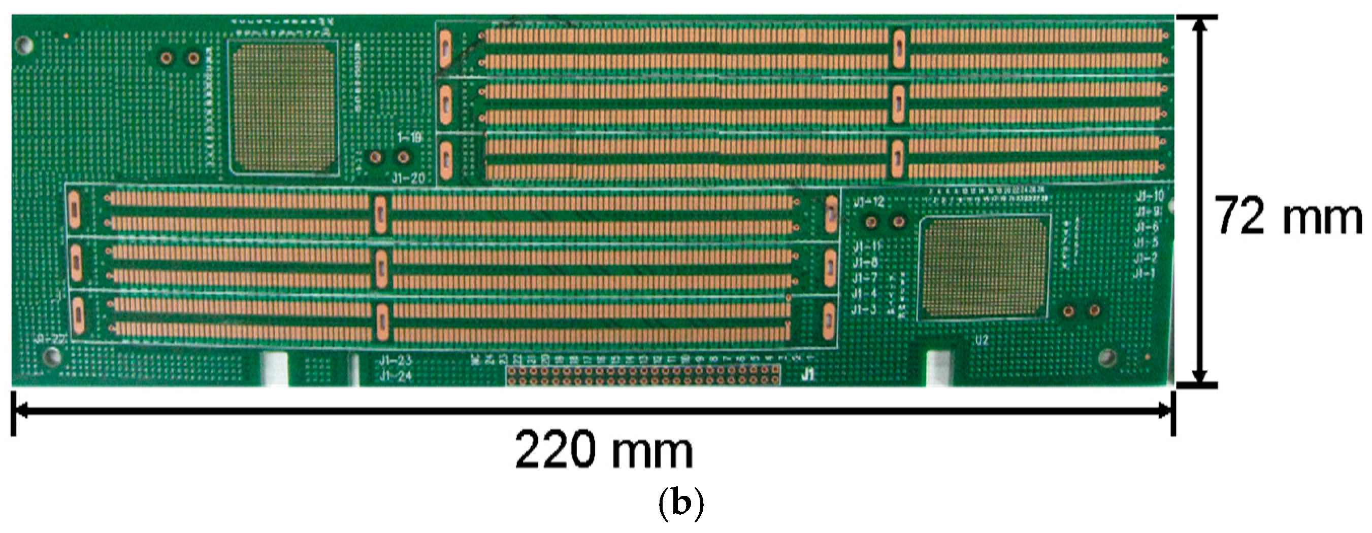
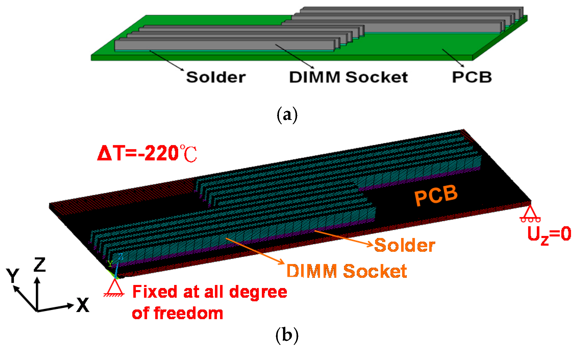
2. Methodologies
3. Results and Discussion
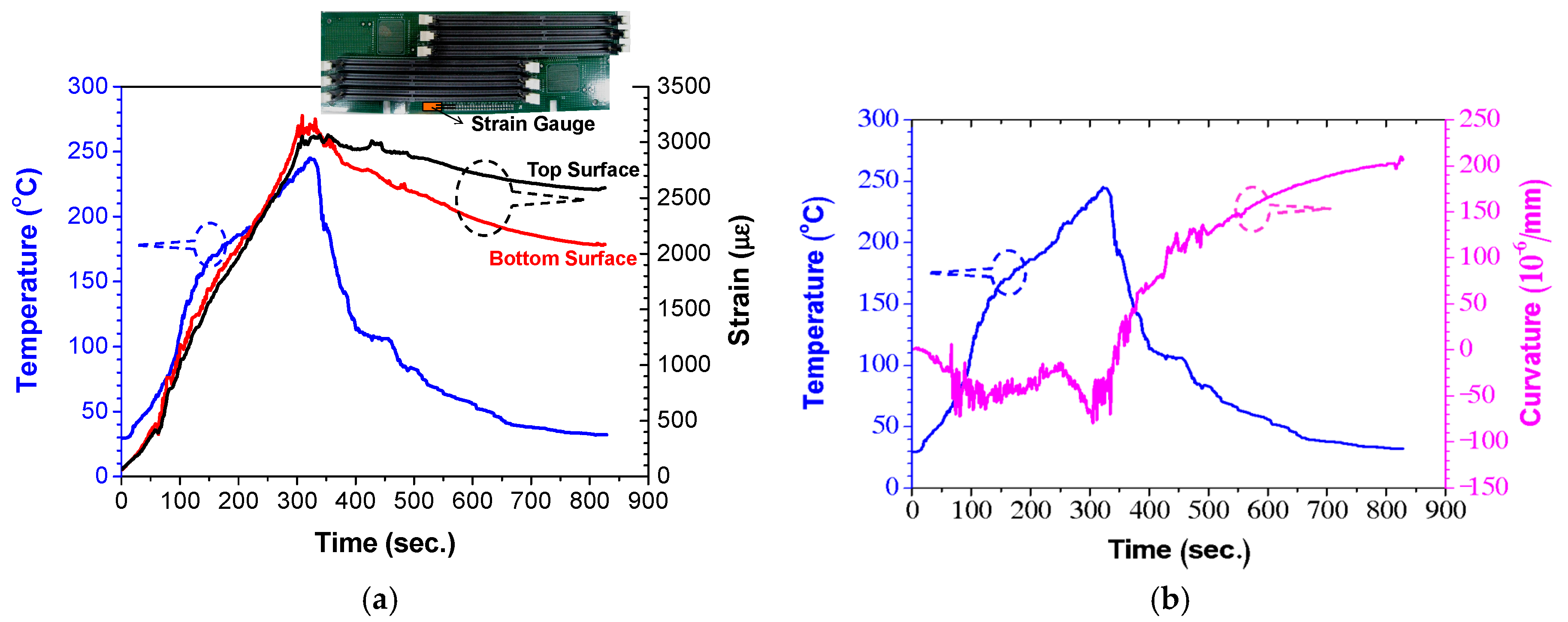
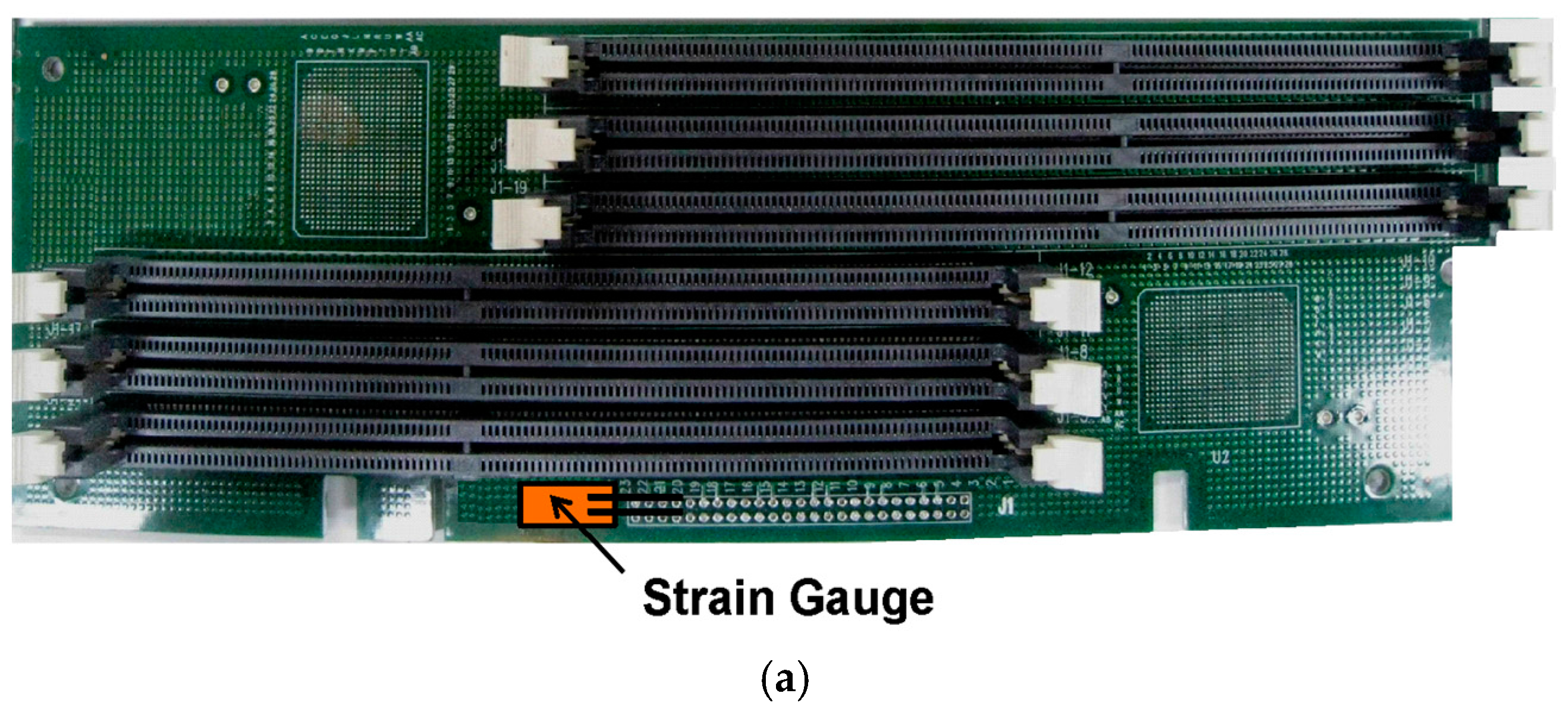
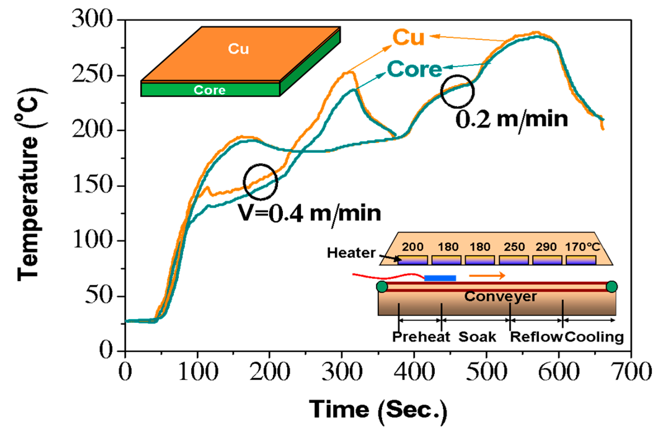
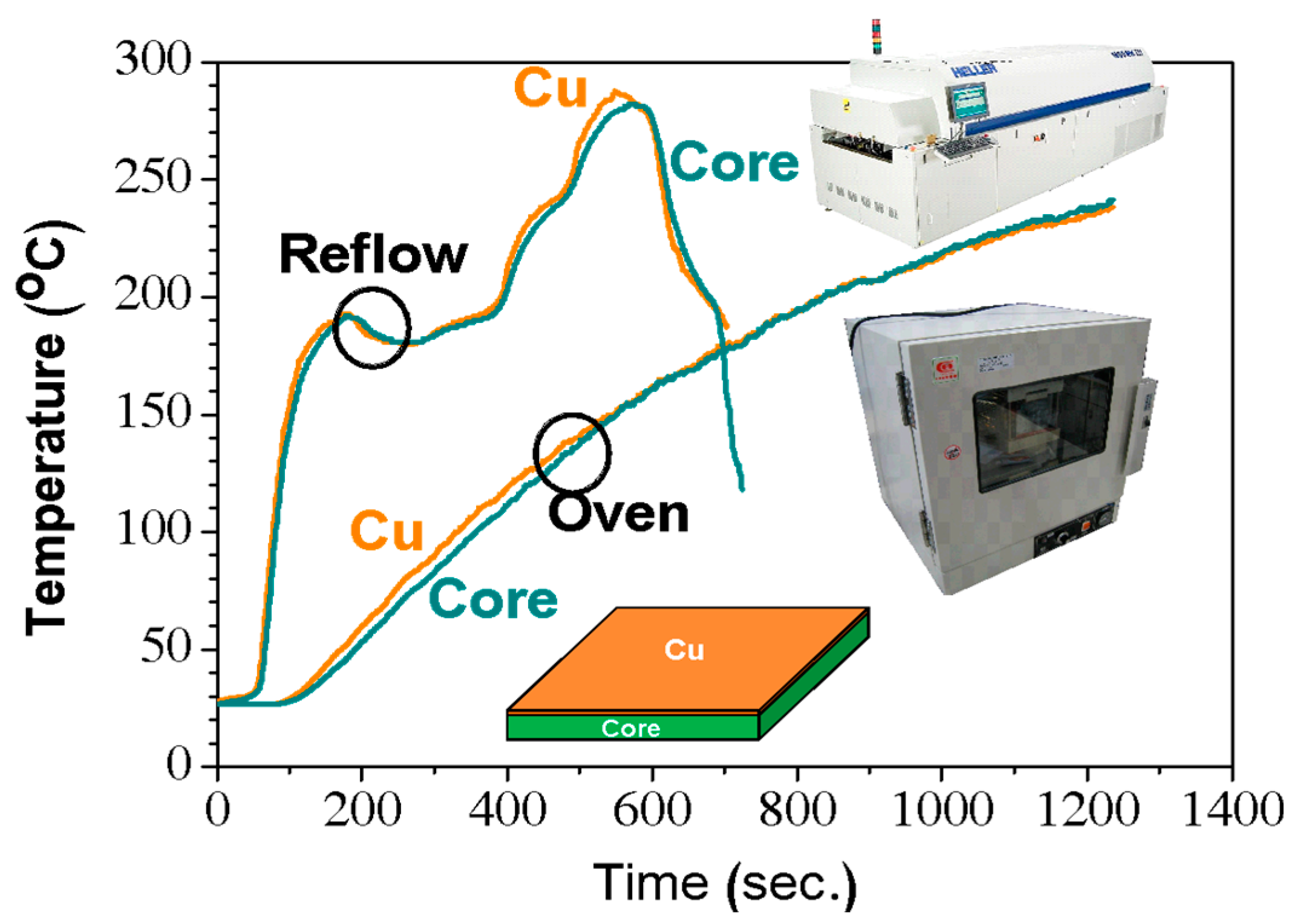
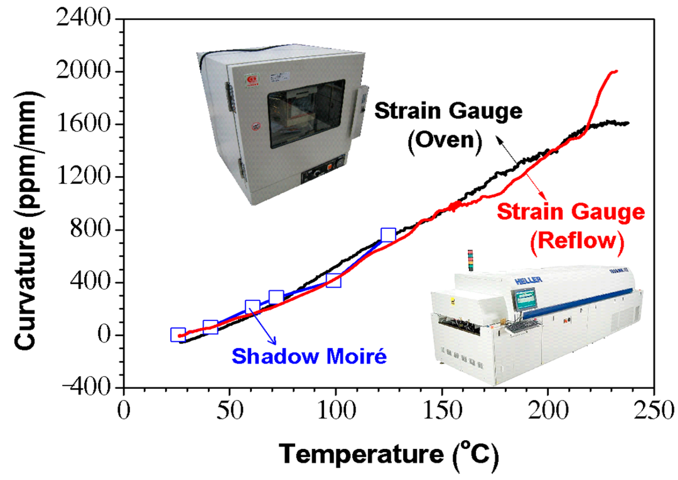
3.1. Thermal and Curvature Data Verifications
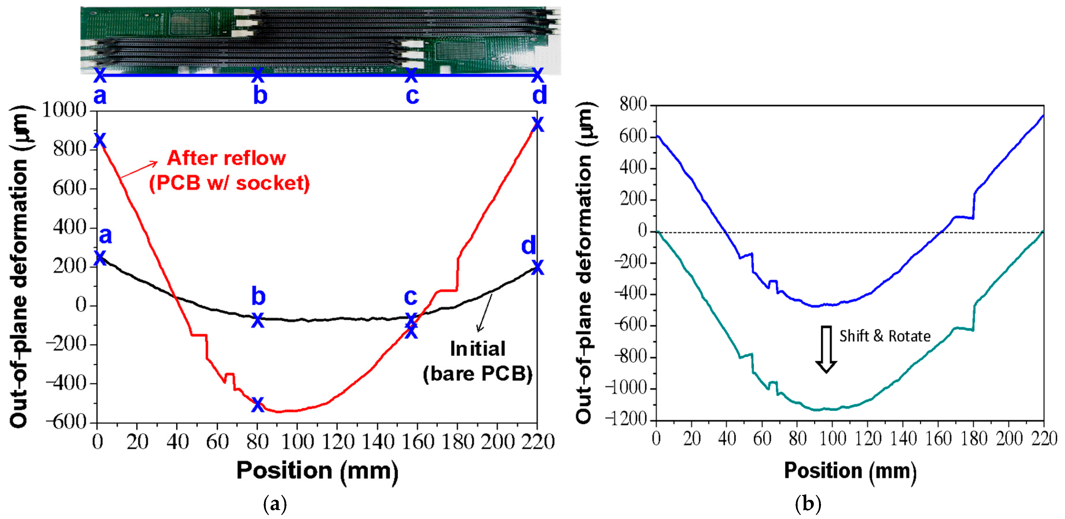
3.2. Measurements of Curvatures and Deformations
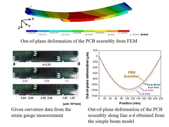
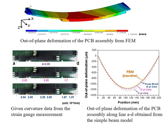
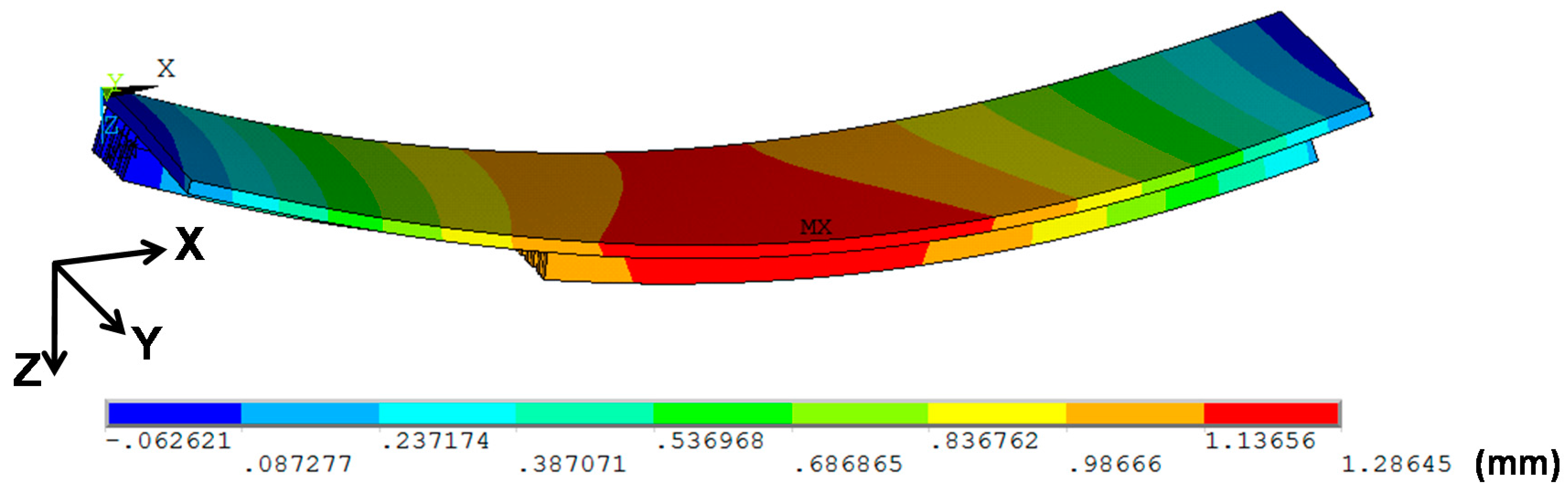
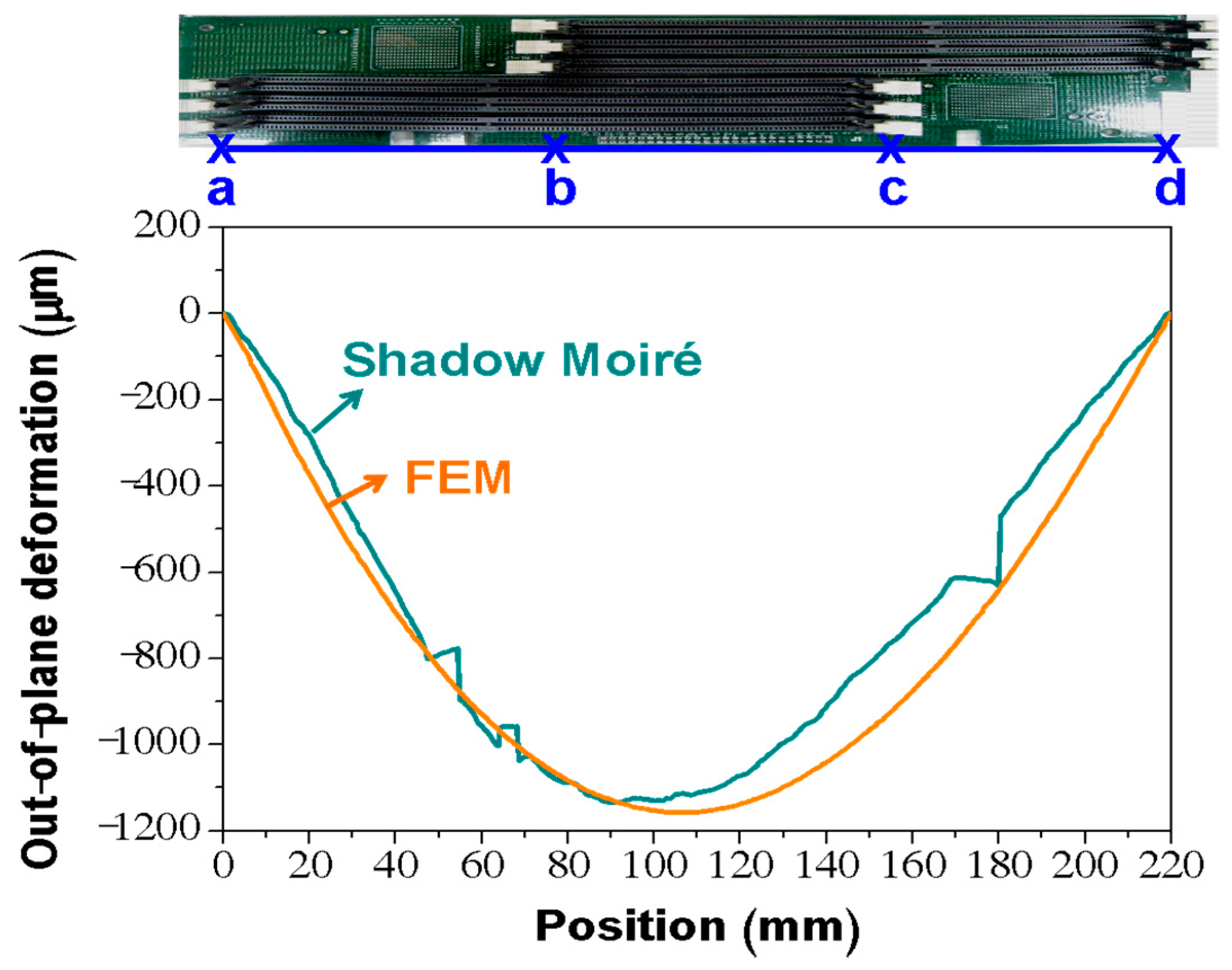
3.3. Deformation Validation by FEM
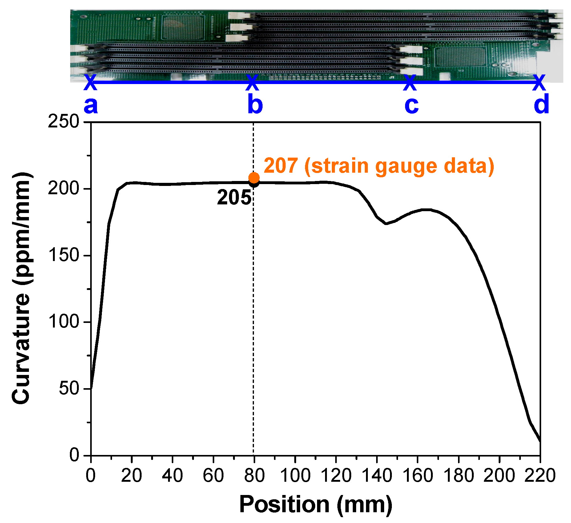
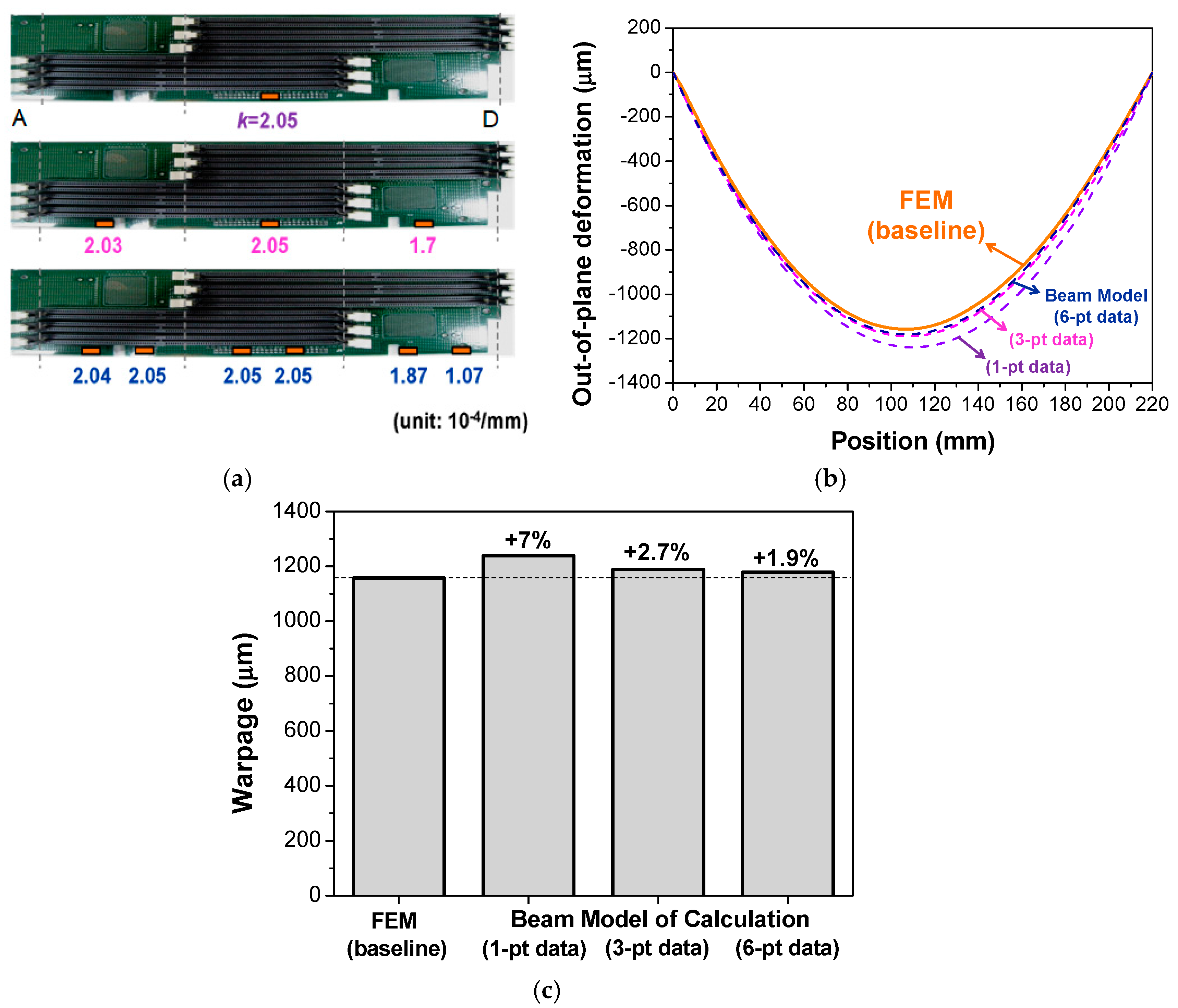
3.4. Construction of Deformation and Warpage Using Gauge Data
4. Conclusions
Acknowledgments
Author Contributions
Conflicts of Interest
References
- Wu, T.Y.; Guo, Y.; Chen, W.T. Thermal-mechanical strain characterization for printed wiring boards. IBM J. Res. Dev. 1993, 37, 621–634. [Google Scholar] [CrossRef]
- Ratanawilai, T.B.; Hunter, B.; Subbarayan, G.; Rose, D. A study on the variation of effective CTE of printed circuit boards through a validated comparison between strain gauges and moiré interferometry. IEEE Trans. Compon. Packag. Technol. 2003, 26, 712–718. [Google Scholar] [CrossRef]
- Pecht, M.G.; Govind, A. In-situ measurements of surface mount IC package deformations during reflow soldering. IEEE Trans. Compon. Packag. Manuf. Technol. 1997, 20, 207–212. [Google Scholar] [CrossRef]
- Mercado, L.L.; Hsieh, G.; Girouard, S. Electronic packaging solder joint reliability assessment with a mechanics-based strain gauge methodology. IEEE Trans. Packag. Technol. 2006, 29, 5–12. [Google Scholar] [CrossRef]
- Shi, H.; Ikezawa, S.; Ueda, T. A novel method for evaluating tri-axial strain gages used in printed circuit board assemblies (PCBA) strain monitoring. In Proceedings of the IEEE Sensor Conference, Limerick, Ireland, 28–31 October 2011. [Google Scholar]
- Wang, Q.; Xie, W.; Ahmad, M. Experimentally validated analysis and parametric optimization of monotonic 4-point bend testing of advanced BGA packages. In Proceedings of the 13th International Conference on Electronic Packaging Technology & High-Density Packaging, Guilin, China, 13–16 August 2012. [Google Scholar]
- Low, S.; Singh, I.; Hariharan, G.; Yip, L.; Zohni, N.; Abtew, M.; Solaiappan, G.S.; Vair, V.; Lewis, S. Mechanical and board level reliability considerations of lidless flip chip BGA packaging. In Proceedings of the IEEE 63rd Electronic Components and Technology Conference, Las Vegas, NV, USA, 28–31 May 2013. [Google Scholar]
- Bhat, S.K.; Deshpande, R.; Beck, P.; Hegde, S.; Upadhyaya, Y.S.; Ghosh, C.K. Study on effect of thermo-structural loading on the PCB during selective soldering process using finite element method. In Proceedings of the 1st International Conference on Energy and Power, Sapporo, Japan, 20–22 April 2016. [Google Scholar]
- Post, D.; Han, B.; Ifju, P. High Sensitivity Moiré Experimental Analysis for Mechanics and Materials; Spring: Berlin, Germany, 1993. [Google Scholar]
- Hai, D.; Powell, R.E.; Hanna, C.R.; Ume, I.C. Warpage measurement comparison using shadow moiré and projection moiré methods. IEEE Trans. Compon. Packag. Technol. 2002, 25, 714–721. [Google Scholar]
- Tsai, M.Y.; Chang, H.Y.; Pecht, M. Warpage analysis of flip-chip PBGA packages subject to thermal loading. IEEE Trans. Device Mater. Reliab. 2009, 9, 419–424. [Google Scholar] [CrossRef]
- Tsai, M.Y.; Ting, C.W.; Huang, C.Y.; Lai, Y.S. Determination of residual strains of the EMC in PBGA during manufacturing and IR solder reflow processes. Microelectron. Reliab. 2011, 51, 642–648. [Google Scholar] [CrossRef]
- Tsai, M.Y.; Chen, Y.C.; Lee, S.W.R. Correlation between measurement and simulation of thermal warpage in PBGA with consideration of molding compound residual strain. IEEE Trans. Compon. Packag. Technol. 2008, 31, 3–683. [Google Scholar]
- Huang, T.C.; Liao, M.C.; Tang, H. CPU socket warpage measurement during reflow temperature variation using shadow moiré. In Proceedings of the IMPACT 2009, Taipei, Taiwan, 12–14 March 2009. [Google Scholar]
- Huang, P.S.; Lin, Y.H.; Huang, C.Y.; Tsai, M.Y.; Huang, T.C.; Liao, M.C. Warpage and curvature determination of PCB with DIMM socket during reflow process by strain gage measurement. In Proceedings of the IMPACT 2010, Taipei, Taiwan, 20–22 October 2010. [Google Scholar]
- Liao, M.C.; Huang, P.S.; Lin, Y.H.; Huang, C.Y.; Tsai, M.Y.; Huang, T.C. Warpage measurements of printed circuit board during reflow process using strain gauges. In Proceedings of the IMPACT 2014, Taipei, Taiwan, 22–24 October 2014. [Google Scholar]


| Material | E (GPa) | α (ppm/°C) | ν |
|---|---|---|---|
| PCB | 20 | 18 | 0.28 |
| DIMM Socket | 19 | 11.3 | 0.3 |
| Solder | 49 | 20 | 0.4 |
© 2017 by the authors. Licensee MDPI, Basel, Switzerland. This article is an open access article distributed under the terms and conditions of the Creative Commons Attribution (CC BY) license (http://creativecommons.org/licenses/by/4.0/).
Share and Cite
Liao, M.-C.; Huang, P.-S.; Lin, Y.-H.; Tsai, M.-Y.; Huang, C.-Y.; Huang, T.-C. Measurements of Thermally-Induced Curvatures and Warpages of Printed Circuit Board during a Solder Reflow Process Using Strain Gauges. Appl. Sci. 2017, 7, 739. https://doi.org/10.3390/app7070739
Liao M-C, Huang P-S, Lin Y-H, Tsai M-Y, Huang C-Y, Huang T-C. Measurements of Thermally-Induced Curvatures and Warpages of Printed Circuit Board during a Solder Reflow Process Using Strain Gauges. Applied Sciences. 2017; 7(7):739. https://doi.org/10.3390/app7070739
Chicago/Turabian StyleLiao, Meng-Chieh, Pu-Shan Huang, Yi-Hsien Lin, Ming-Yi Tsai, Chen-Yu Huang, and Te-Chin Huang. 2017. "Measurements of Thermally-Induced Curvatures and Warpages of Printed Circuit Board during a Solder Reflow Process Using Strain Gauges" Applied Sciences 7, no. 7: 739. https://doi.org/10.3390/app7070739
APA StyleLiao, M.-C., Huang, P.-S., Lin, Y.-H., Tsai, M.-Y., Huang, C.-Y., & Huang, T.-C. (2017). Measurements of Thermally-Induced Curvatures and Warpages of Printed Circuit Board during a Solder Reflow Process Using Strain Gauges. Applied Sciences, 7(7), 739. https://doi.org/10.3390/app7070739