Comparison of Basic Notch Filters for Semiconductor Optical Amplifier Pattern Effect Mitigation

1
Democritus University of Thrace, Department of Electrical and Computer Engineering, Laboratory of Telecommunications Systems, Lightwave Communications Research Group, Xanthi 67 100, Greece
2
Technological Educational Institute of Chalkis, Department of Aircraft Technology, Chalkis 34 100, Greece
*
Author to whom correspondence should be addressed.
Appl. Sci. 2017, 7(8), 783; https://doi.org/10.3390/app7080783
Submission received: 12 July 2017
/
Revised: 28 July 2017
/
Accepted: 28 July 2017
/
Published: 2 August 2017
(This article belongs to the Special Issue Applications of Semiconductor Optical Amplifiers)
Abstract
:We conduct a thorough comparison of two basic notch filters employed to mitigate the pattern effect that manifests when semiconductor optical amplifiers (SOAs) serve linear amplification purposes. The filters are implemented using as the building architecture the optical delay interferometer (ODI) and the microring resonator (MRR). We formulate and follow a rational procedure, which involves identifying and applying the appropriate conditions for the filters’ spectral response slope related to the SOA pattern effect suppression mechanism. We thus extract the values of the free spectral range and detuning of each filter, which allow one to equivocally realize the pursued comparison. We define suitable performance metrics and obtain simulation results for each filter. The quantitative comparison reveals that most employed metrics are better with the MRR than with the ODI. Although the difference in performance is small, it is sufficient to justify considering also using the MRR for the intended purpose. Finally, we concisely discuss practical implementation issues of these notch filters and further make a qualitative comparison between them in terms of their inherent advantages and disadvantages. This discussion reveals that each scheme has distinct features that render it appropriate for supporting SOA direct signal amplification applications with a suppressed pattern effect.
1. Introduction
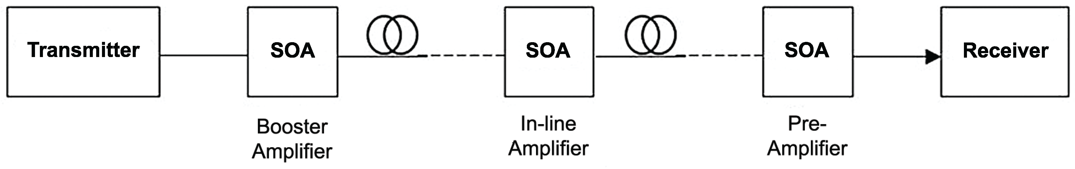
Optical amplifiers (OAs) are key elements for the development, implementation and evolution of fiber-based transportation, distribution and access networks [1,2]. Their traditional functions include (Figure 1 [3]) enhancing the signal power before being launched into an optical link (boosters), compensating for signal losses incurred either by the fiber medium, components along the propagation path or optical splitters, branches and taps (in-line reach extenders) and increasing the level of the received signal before photodetection (preamplifiers).
In this manner, they decisively contribute to achieving high global capacities, long transmission spans, multipoint-to-multipoint connectivity and ubiquitous information availability. These are critical requirements for efficiently coping with the growing data volumes and the diverse users’ needs that govern the changeable broadband environment. Especially OAs that exploit semiconductor materials in the form of ‘SOA’ devices have been enjoying continuous preference by the optical communications research [4] and commercial (see indicatively [5]) sectors. The reason for this fact stems from SOAs’ potential for signal amplification and multi-functionality entirely in the optical domain, within a broad wavelength range, with low power consumption, in a tiny volume at reasonable cost.
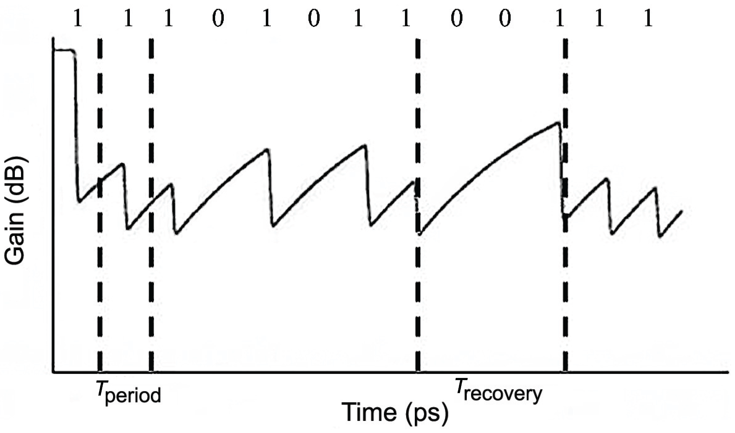
Despite SOAs attractive features, the employment of these elements for the aforementioned linear amplification purposes in diverse applications, such as optical transmission [6], radio over fiber [7], passive optical networks [8], optical wireless communications [9], optical data interconnects [10], converged metro-access networks with heterogeneous services [11] and burst information handling [12], has been compromised by SOAs carrier lifetime, which is finite [3]. When this physical parameter is comparable to the repetition period of the SOA driving data, as is often the case, it dominates the time scale of the SOA gain dynamics. Thus, if the combination of the power and duration of the input data signal is such that the SOA is deeply saturated, then the SOA gain is not perturbed and recovered in the same way for all excitation pulses (Figure 2).
As a consequence, the SOA operation becomes pattern dependent so that the amplification received by a given bit does not depend solely on this input, but also on the history of the SOA response to previous bits. This undesirable situation is referred to as the ‘pattern effect’ (PE) [13] and is more pronounced for data pulses that occupy a fraction of the assigned bit slot, i.e., of return-to-zero (RZ) data format, and hence, impose a heavy strain on the SOA gain dynamics [14]. Due to the PE, the profile of the pulses at the SOA output is not uniform, since pulses are distorted by peak-to-peak amplitude fluctuations, and therefore is far from ideally being an amplified replica of the input signal (Figure 3).
In order to allow conventional SOAs to fulfil their classical role, it is necessary to combat the PE and its deleterious consequences. For RZ pulses, this requires lowering their power well below the SOA strong saturation regime, as well as substantially shortening their width [15]. These actions are not sufficient since the first one results in a poor optical signal-to-noise ratio (OSNR), reduced maximum output power, closer amplifier spacings and narrower input power dynamic range (IPDR) [16], while the second one requires applying intricate ultrafast pulse generation approaches [17] and dealing with practical related issues, such as nonlinear effects [18] and intraband phenomena [19].
Among the various methods that have been proposed to improve the pattern-dependent performance of SOAs used for direct signal amplification (see [15] and the relevant references therein), optical filtering has attracted intense research interest [20,21,22,23,24,25]. This passive method has been conceived of based on the observation that pulse amplification in an SOA is accompanied by spectral broadening to longer wavelengths (red shift) due to the manifestation of self-phase modulation (SPM) [26]. The SPM-induced spectral shift to longer wavelengths is higher than for the lower amplitude amplified pulses. This means that placing an optical filter after the SOA to pass a larger portion of the broadened spectrum for the less intense amplified pulses while blocking it for the more intense amplified pulses can compensate for the uneven red shift, which is converted then by the filter’s slope [27] into more equalized pulse peak amplitudes (Figure 3).
During last few years, we have applied the optical filtering technique for SOA pattern effect suppression by means of a platform comprised of different notch filters [15,28,29,30,31,32,33]. Among these filters, we particularly distinguish the optical delay interferometer (ODI) [30,31,32] and the microring resonator (MRR) [33], which share several common features, such as an all-optical and passive nature, simple structure, compatibility both with fiber medium and microelectronic fabrication processes, compact size, periodic and tunable transfer function and potential for integration and co-packaging with the SOA in a single module. These filters have conventionally been destined to serve more classical filter-oriented applications. However, in this paper, we do not treat them individually, but in conjunction with the SOA and the serious PE problem of the latter, which they intend to solve. Since the MRR has recently received intense interest and is being widely exploited in numerous and diverse light wave applications, but the ODI has been employed more for assisting the SOA operation, it would be useful to investigate and assess whether this trend of shifting to the MRR technology should be extended to the mitigation of the SOA PE. To this aim, we conduct a quantitative and qualitative comparison of the ODI and MRR capability to confront the SOA pattern effect, thereby completing our work on the specific research topic. The comparison reveals that although the ODI suitability for the intended goal has been well tested and confirmed, both theoretically and experimentally, the MRR can realize better improvements in a set of key performance criteria and features several better operating characteristics than the ODI. This indicates that the MRR also has the technological potential to contribute in equal terms with its ODI counterpart for resolving the complications provoked by the SOA pattern effect.
2. Basic Optical Notch Filters’ Configurations
The considered basic optical notch filters differ in their construction and operation and accordingly in the way that their spectral response is obtained and tailored for suppressing the SOA pattern effect.
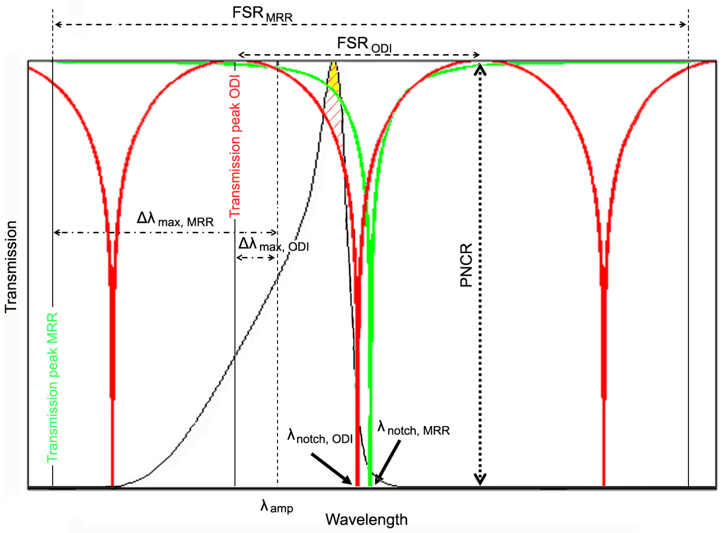
The ODI’s principle of operation relies on splitting, delaying and recombining the amplified signal, which is a process realized by means of intensity discrimination. Other waveguide-based technologies, which have been used for performing these functions in the wavelength domain, are reported in [34,35,36,37,38]. As shown in Figure 4a, it is constructed from two 3-dB couplers by interconnecting the output ports of the first one to the respective input ports of the second one. The upper arm of the formed interferometric configuration has a relative delay, , against the second arm, into which a phase bias, , is introduced. When the amplified signal is inserted in the ODI from the first coupler, it is halved into two identical copies, which follow distinct paths along the ODI and acquire a wavelength-dependent phase difference analogous to their relative delay. Thus, when these components recombine at the second coupler, they interfere either constructively or destructively and produce at the ODI crossed output port the spectral response shown in Figure 5 with red color. The wavelength separation between adjacent maxima (peaks), or the free spectral range (FSR), is inversely proportional to the ODI relative delay, i.e., [32], where is the reference optical wavelength of the amplified signal, which lies in the vicinity of 1550 nm, and c is the speed of light in a vacuum. The minima (notches) are located halfway between maxima, and their exact wavelength position with respect to the shorter (blue) or longer (red) sideband, indicated by in Figure 5, depends on the phase bias, . This determines the wavelength detuning of the data carrier from the nearest transmission peak, , according to [39].
The MRR is a waveguide shaped into a ring structure that is coupled to a bus waveguide, as shown in Figure 4b. When a signal enters this configuration, part of it is fed back to the MRR input while the rest is transferred at the MRR output. The exact signal magnitude and wavelength that penetrate into the ring depend on the strength of coupling between the straight and circular waveguides and whether the condition of resonance is satisfied. The amplified signal components that enter the ring subject to these conditions travel around it and after a time delay proportional to the ring circumference interfere with those components that pass directly to the exit. Then, provided that the MRR operates in the so-called critical coupling regime, where the field transmission coefficient, r, and the amplitude attenuation factor, l, are equal, the circulating intensity is maximized, and the transmitted intensity becomes minimum [33]. As a result, the spectral response shown with green color in Figure 5 is obtained. The notches, which are located at , occur at resonance according to the condition , where R is the MRR radius, is the waveguide effective refractive index and m is a non-zero integer. The wavelength distance between consecutive maxima is given by . The spectral alignment of the transmission maximum, relative to the data carrier, , which, analogously to the ODI, corresponds to a phase bias , can be varied within half FSR towards the blue or red sideband by tuning the MRR resonant wavelength through various appropriate mechanisms [40].
3. Optical Notch Filter Requirements for SOA Pattern Effect Suppression
The profiles of the ODI and MMR spectral responses in Figure 5 allow both schemes to act as optical notch filters for mitigating the SOA pattern-dependent performance degradation. For this purpose, it is necessary to suitably tailor the spectral characteristics of these responses so that the spectral components of the amplified pulses are forced to lie close to the notches and, hence, are suppressed in direct analogy to the degree of their red shift. This involves choosing and controlling the wavelength spacing (FSR), the contrast and the position of the notches, according to the following requirements [33]: (1) The FSR must be such that the notches are not spaced too close or too far, but sufficiently apart. Thus, making the FSR either too small or large prevents the red-shifted components of the amplified signal from distinctly falling along the response’s slope and accordingly from being filtered analogously to their SPM-induced spectral magnitude. Instead, the FSR must be chosen so as to ensure that: (a) there is a sufficiently wide margin available for the red-shifted spectral components to be contained within the spectral borders defined by the difference and ; (b) the passband width is neither too narrow nor too broad so that the red-shifted spectral components do not fall outside or are loosely acted upon, respectively; (c) the suppression exerted by the filter on these components scales with the uneven peak amplitude they originate from, in order to clamp the higher amplitude amplified pulses while comparatively enhancing the lower amplitude ones; (d) the notches antipodes, i.e., the transmission peaks, are close enough so that the reference data wavelength can fall in their vicinity and perceive a sufficient fraction of the transmission maximum. In this manner, the amplified signal can pass through the notch filter without suffering a significant reduction in its amplitude or equivalently without significant elimination of the useful information it carries [21], which is critical when employing spectral elimination techniques for combating signal impairments [24]. (2) The repetitive notches must be sharp and deep enough to maximize their magnitude difference from their adjacent transmission peaks, which defines the peak-to-notch contrast ratio (PNCR) and ensure that the asymmetrically-broadened spectral components after the SOA are suppressed not weakly, but strongly and not identically, but to an extent directly dependent on the position in the data stream of the pulse from which they originate. (3) The notches must occur at a higher wavelength than that of the amplified signal, so that the transmittance is decreased as the wavelength is increased. This is again indispensable in order for the spectrally-broadened components to be suppressed analogously to the degree of their red shift.
4. ODI vs. MRR Comparison Rationale
In order to realize the comparison between the ODI and MRR, we must select and assign the proper values to the parameters that critically affect their operation, i.e., (, ) and (R, ), respectively, so that this comparison is done on a fair basis. For this purpose a rational approach is adopted, which is followed after suitably combining the evidence available and knowledge that have been acquired, both theoretically and experimentally, on these types of modules when employed as notch filters. To this aim, the starting point is to equate the maximum slope of their spectral responses. Taking this as the comparison criterion is dictated by the SOA pattern effect suppression filtering mechanism, according to which the irregularly-shifted spectral components of the amplified pulses are converted by each filter’s slope into amplitude changes, which counteract those incurred by the SOA ([27], cf. Figure 4.18). On the other hand, the maximum slope is related to the sensitivity of these filters to input signal perturbations, like those after the SOA, and accordingly to their capability to handle and compensate them [41]. Then, the maximum slope can be determined by finding the zeros of the second derivative of each filter’s transfer function and replacing them into the first derivative. This procedure, which is conveniently executed in the angular frequency domain, leads to the equality:
where the left-hand side gives the maximum slope at critical coupling of the MRR ([42], cf. Equations (3.11)–(3.12) and (B.9)), whose round-trip delay is , while the right-hand side represents the same quantity for the ODI [15]. Letting then , so as to ensure that the condition of critical coupling for the MRR is favorably met, but also to preserve the continuity with previous relevant work [33], leads to:
which readily gives ps, or equivalently, um, for ps, where the latter value has not been arbitrarily chosen, but according to the selection rules derived in [31] for the conditions under which the ODI should operate to combat the SOA pattern effect. Similarly, the calculated MRR radius complies with the permissible range of values specified for this parameter from the study in [33]. Furthermore, and R are such that the filtered-out data pulses retain their initial shape, as addressed in [15,29] and verified again below. Having determined the FSR of the ODI and MRR, the next step is to do the same for their detuning. This can be done by applying the criterion of equalization of the red-shifted components of the amplified signal, which must hold in order for the low-pass frequency characteristic of the SOA to be compensated by the high-pass frequency characteristic of the two employed notch filters ([27], cf. Figure 4.4). In this context, the filters’ intensity response, , is Taylor-expanded to the first order around , thus leading to the following requirement in the linear scale for the filters’ slope magnitude, K, [43], which governs the efficiency of converting the uneven SPM-induced spectral broadening to uniform amplified pulse amplitude [44]:
This relationship essentially expresses in mathematical terms the fact that the SOA temporal response, which is limited by the SOA finite carrier lifetime, , and the associated pattern effect, can be enhanced by means of the employed filters by a factor that scales at most with the SOA linewidth enhancement factor, [45]. Then, using the electric field responses [40,46]:
for the ODI and MRR, respectively, and substituting in (3) yields, after appropriate algebraic manipulations and numerical calculations for ps and , and . Note that the MRR phase bias has mathematically been shifted by ‘’, so that the transfer functions of both considered filters become null when the wavelength position of the input data carrier coincides with that of the nearest notch, which happens when . These phase bias values correspond to nm and nm. The difference in the detuning values is attributed to the fact that, as shown in Figure 5, the ODI and MRR have different FSR, i.e., . Furthermore, they imply that is closer to than , since nm while nm.
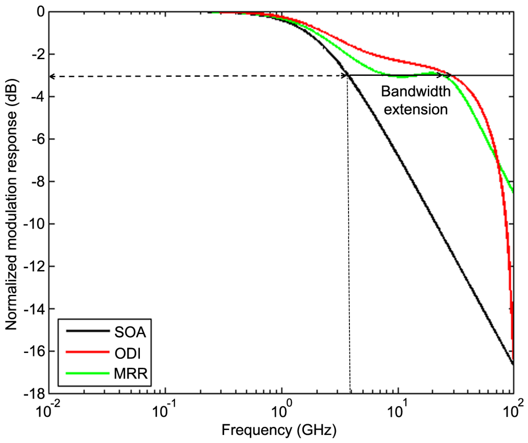
The suitability of the critical parameters values specified above is further verified by observing that both filters extended the modulation response bandwidth of the SOA, which is inherently limited by the SOA finite carrier lifetime responsible for the pattern effects. This is shown in Figure 6, which has been obtained by plotting first the modulation response of the stand-alone SOA and then combining it in a multiplicative manner with that of the ODI or MRR. These responses are mathematically described by closed-form expressions obtained through appropriate small-signal analysis, which allows one to find for each module the transfer function between small signal changes of the output power incurred by small-signal perturbations of the input power, as reported in [47] for the SOA and ODI and in [48] for the MRR.
5. ODI vs. MRR Comparison: Results and Discussion
The ODI and MRR are compared using appropriate performance metrics, which allow one to assess the performance of an SOA subject to a strong pattern effect and subsequently the capability of the employed notch filtering schemes to suppress it. These metrics include: (a) The amplitude modulation (), which is defined as (dB) , where () is the peak power of the mark across the amplified data stream, which has the highest (lowest) amplitude level [30]. The provides a measure of the degree of uniformity of the amplified pulses whose pattern-dependent pulse-to-pulse wandering should be reduced by the employed filters below 1 dB [49]. (b) The amplification reduction (), which is defined as (dB) (dBm)(dBm)|, where and are the total average powers at the ODI or MRR filters and SOA outputs, respectively: The takes into account the fact that, due to the suppression of the red-shifted components by the action of filtering, some useful information contained in them is inevitably lost [21]. This causes the data sequence to receive less amplification than after the SOA alone, which is translated into an amplification penalty [50] that is quantified by the . Ideally, the extent of must be such that it can be compensated by the average gain offered by the SOA to the data stream and accordingly allow the net gain of the SOA-notch filter combination to be sufficient for direct signal amplification purposes. (c) The cross-correlation () coefficient, which is defined as [51], where the symbol of the caret over the time-dependent powers denotes that the latter are normalized to their maximum value: The is a measure of the degree of similarity of the intensity profile of the amplified signal that is filtered by the ODI or MRR to its profile prior to being inserted in the SOA. The higher the , the better is the capability of the given filter to accurately reproduce the original signal. (d) The -factor represents the OSNR at the input of the receiver decision circuit: in the thermal noise limit [52], where the amplitude fluctuations due to the pattern effect act as noise variance on the marks [19], , where is the average and is the standard deviation of the peak power of the marks and OSNR . Because the OSNR is measured in units of decibels (dB), it is convenient to use the same dimensioning for the Q-factor. Thus, 101og(OSNR (dB). On the other hand, the Q-factor value in the linear scale must be at least six to ensure that the associated bit error rate is less than [52] and error-free operation can be achieved. Converting this requirement into logarithmic scale results in (dB) dB, which therefore is the limit against which the specific employed metric is addressed in the rest of the paper. Then, it is possible to determine: (i) the input power dynamic range (IPDR) [53]; (ii) the permissible variation from the specified detuning; and (iii) the maximum signal transmission distance in standard single-mode fiber (SSMF) without dispersion compensation. The signal powers involved in the above definitions can be found through simulation run at 10 Gb/s. This bit rate is in line with data rates of modern applications that exploit SOAs as linear amplification elements [2,8] and falls in the range within which significant bit pattern distortions are caused on signals directly amplified by typical SOAs [54]. The input to the SOA is a pseudo random binary sequence (PRBS) of 127 bits in length, which allows one to fully capture and investigate the detrimental impact of the SOA pattern effect [55]. This data stream contains Gaussian-shaped RZ pulses of such duty cycle and peak power that together saturate heavily the SOA and provoke a strong pattern effect at its output [31]. The default parameters values used in the simulation are those reported in [31,33]. The simulation procedure involves [15,33] numerically calculating the SOA integrated gain temporal response, substituting the outcome in the electric field (normalized so that its squared modulus represents power [26]) of the optical signal at the SOA output, applying fast Fourier transform (FFT) to pass it into the frequency domain, convolving it with the ODI or MRR spectral response given from (4) and finally converting the convolution product back into the time domain using inverse FFT (IFFT). The FFT and IFFT operations are available and executed in MATLAB software. The calculation of the -factor is done according to the method described in [15]. The integrals involved in the definition of are numerically calculated in MATLAB using Simpson’s rule.
Figure 7, Figure 8, Figure 9, Figure 10 and Figure 11 show the simulation results obtained for each notch filter. To facilitate comparison, the waveforms and curves have been placed in the same figure with differently colored lines, i.e., red for the ODI and green for the MRR. From these graphical and numerical results, the following concise comments can be made with regard to each performance metric and accordingly to the SOA pattern effect suppression capability of the ODI and MRR:
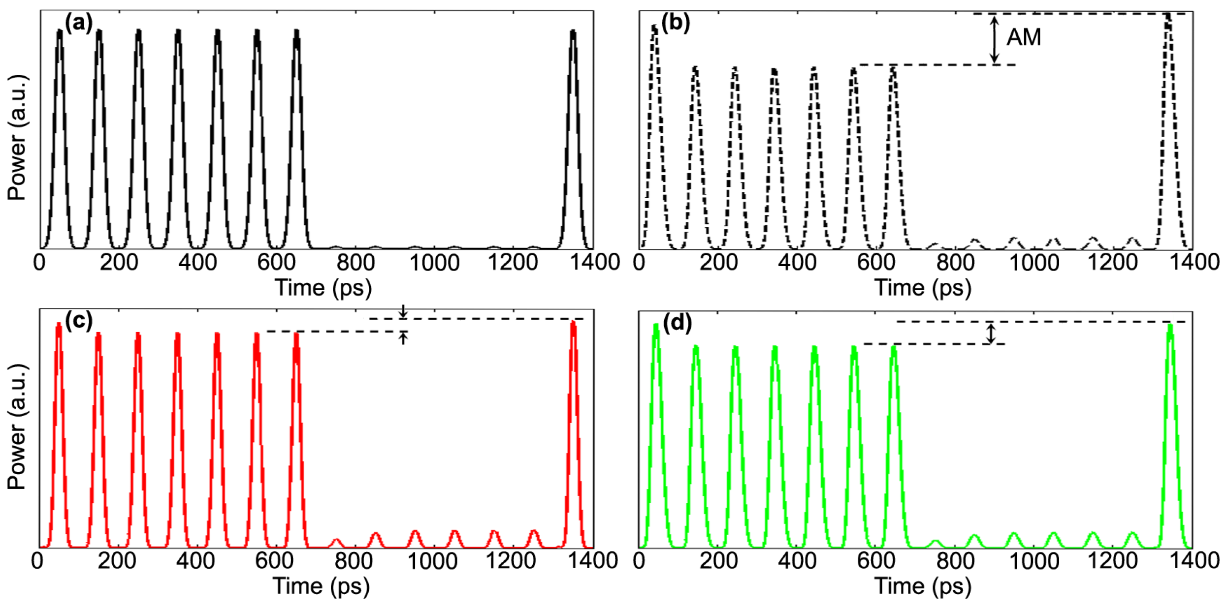
(a) : Both filters can improve this metric and render it acceptable even between the ‘1’ that follows after the longest string of repeated ‘0’s, i.e., six in our case [56], and the ‘1’ that appears just before this run, but also after the same number of consecutive ‘1’s (Figure 7a). In fact, the between the target marks is reduced from 1.15 dB after the SOA (Figure 7b) to 0.22 dB by the ODI (Figure 7c) and to 0.34 dB by the MRR (Figure 7d), which therefore indicates that this demanding situation can equally be confronted with success. The stronger suppression of the achieved by the ODI is justified by the fact that, for the specified detuning values, the notch lies closer to the reference optical wavelength than for the MRR. Consequently, the ODI filters a greater portion of the broadened spectrum of the amplified signal, as indicated in Figure 5 by the red-colored oblique-line zone versus the yellow-colored zone for the MRR. This enhances the amplitude equalization of the spectral components that have asymmetrically been shifted to the longer sideband, but as explained in the following, this enhancement is compromised by the higher and the accompanying performance implications. Although the difference in the reduction of the seems to be small between the two filters, it is not insignificant. In fact, it may become important when cascading several SOAs [12,57], where the peak amplitude differences between amplified pulses should be prevented from being accumulated from stage to stage so that they do not become detrimental for the optical transmission performance.
(b) : Although the ODI filters more spectral components, as explained in (a), this also means that a greater portion of useful information contained in these components is inevitably lost. As a by-product, the data sequence receives less amplification than after the SOA alone, which is translated into an analogous difference between the of the two filters, i.e., 3 dB for the ODI and 2.78 dB for the MRR. This in turn affects the net gain of the SOA-notch filter system, which is further lowered by the losses inserted by each type of filter [15]. Although the loss per length unit of the MRR and the ODI is comparable [58,59], taking into account the significantly longer propagation length of the ODI, which is required in order to create the necessary length imbalance between its two arms, it can be deduced that the total losses exceed by a magnitude order of 3 dB those of the MRR, which are extremely low owing to the much smaller size of the latter. Thus, for the ODI, it is necessary to compensate for its increased losses by adjusting the SOA to provide more gain, which, as explained in [15], is an action that does not impair the capability of this notch filter to suppress the . This extra gain can be offered by supplying more carriers via a higher bias current [8], but at the inevitable expense of increased power consumption. Accordingly, if insertion losses (IL) are included, the MRR allows the SOA-filter system to exhibit a higher net gain [15], i.e., 12.13 dB vs. 8.91 dB for the ODI.
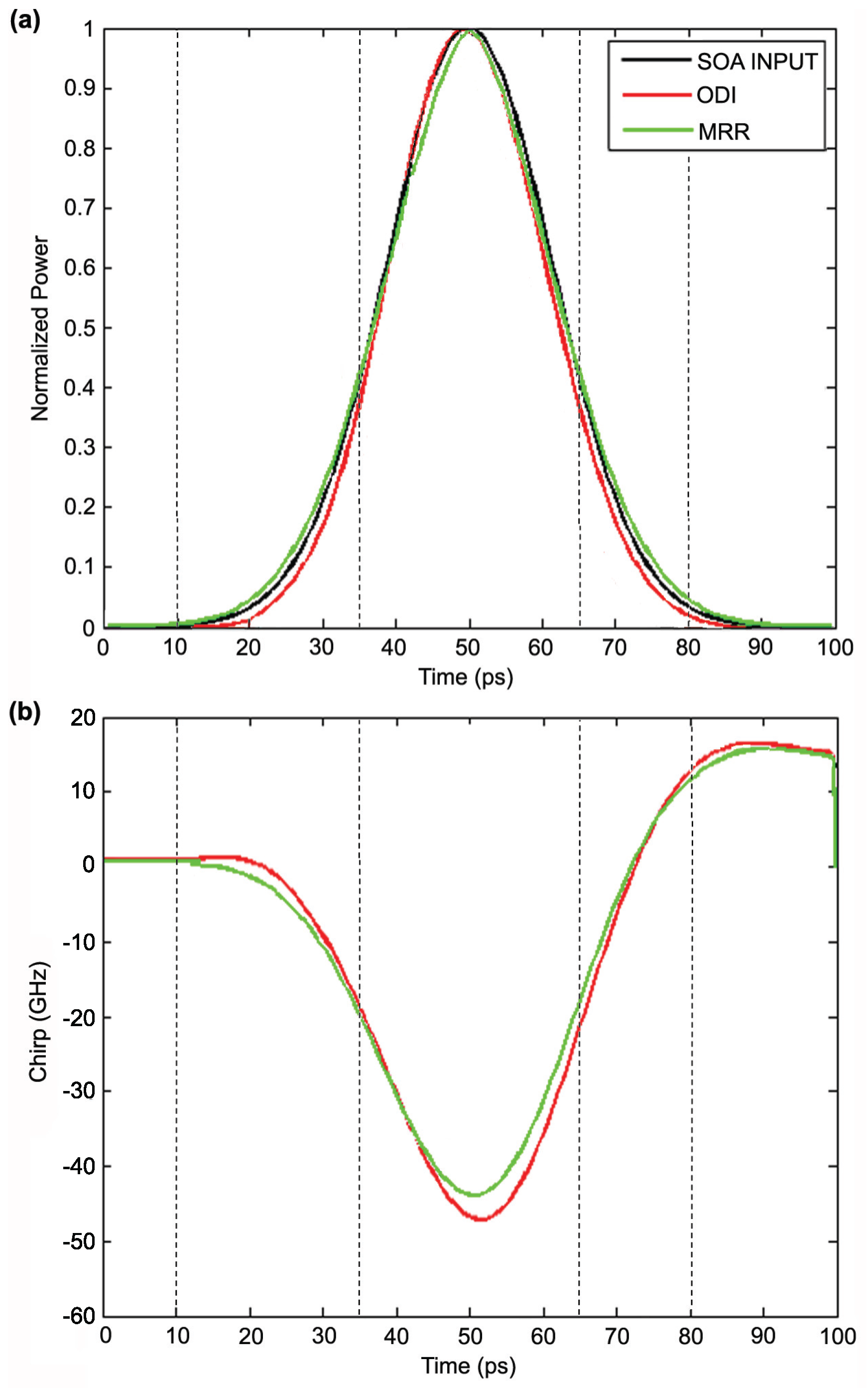
(c) : The numerically-obtained values, 97% for the MRR and 93% for the ODI, indicate that in both cases, the filtered pulse temporal waveform deviates only by 3% and 7%, respectively, from that at the SOA input. This degree of matching implies that the Gaussian-like power profile of the input data pulses is strongly preserved at the filters’ output. This is visually confirmed in Figure 8a, which shows that the envelope of an isolated data pulse maintains its original form. However, the time-bandwidth product at the output of both filters is over the minimum defined for Gaussian-shaped pulses [52], which means that the filtered pulses become chirped. The profile of this chirp, which is shown in Figure 8b, reflects the qualitative differences in the data pulse profiles of Figure 8a. More specifically, in the pulse rising part (region of 10–35 ps), the chirp declines to negative values, i.e., red chirp, but this drop is more dominant for the ODI than for the MRR. This partly explains why the AMattained with the former notch filter is lower than that achieved with the latter. As the pulse continues to temporally evolve, the chirp is decreased more strongly for the ODI until we reach the pulse center, where its absolute magnitude becomes maximum. From this point onwards the situation is reversed and the chirp begins to incline with a slope that is sharper for the ODI than for the MRR. Consequently, and as explained in detail below, the chirp parameter is larger for the ODI, which has a negative impact on the transmission performance of this notch filter in the presence of fiber dispersion. Finally, as we move off the pulse center and approach the pulse falling part (region of 65–80 ps), the chirp changes sign and becomes positive, i.e., blue chirp, which, nevertheless, because of its different cause and time scale over its red chirp counterpart, is not of major concern with regard to the SOA pattern effect suppression [31].
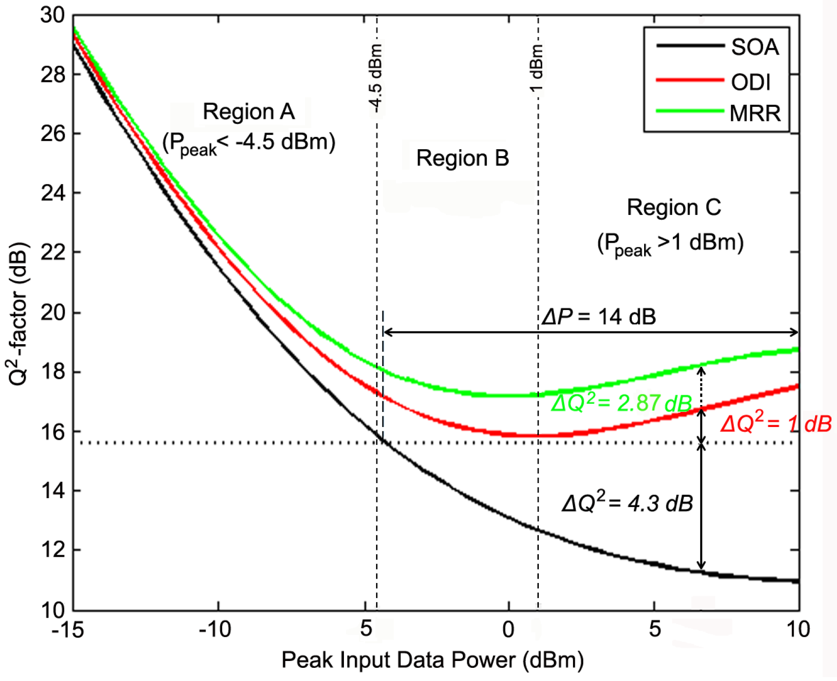
(d) -factor and associated metrics: (i) both filters enhance the IPDR and extend the SOA error-and distortion-free operation from the low saturation region (A in Figure 9) to the deep saturation region (C in Figure 9), in which the SOA gain is decreased by more than 3 dB and 6 dB, respectively. This fact allows one to passively relax the stringent management [60,61] of the input power levels going into the SOA and hence of the degree of SOA gain saturation, which otherwise is required in order to allow SOAs to deliver unimpaired linear amplification functionality. This improvement is realized for both filters, as quantified by the increase of the peak input data power () by dB (assuming a maximum power of 10 dBm going into the SOA). Furthermore, at dBm, which heavily saturates the SOA [31], the -factor is over its critical limit, which for the SOA alone fell short by dB. This is better achieved for the MRR than for the ODI, i.e., dB and dB, respectively.
(ii) The MRR exhibits better tolerance to detuning offset than the ODI, which is an important feature as it obviates the need for resorting to electronic equalization [44]. In fact, Figure 10 shows that the (negative) detuning of the MRR can be varied within 0.12 nm or equivalently by 50% further for the data pulses wavelength modulation bandwidth [52] in the C-band and still keep the -factor acceptable. The corresponding variation for the ODI is comparatively reduced by more than 50%, i.e., 0.05 nm, and hence is narrower, which may impose tighter requirements with regard to wavelength locking [62].
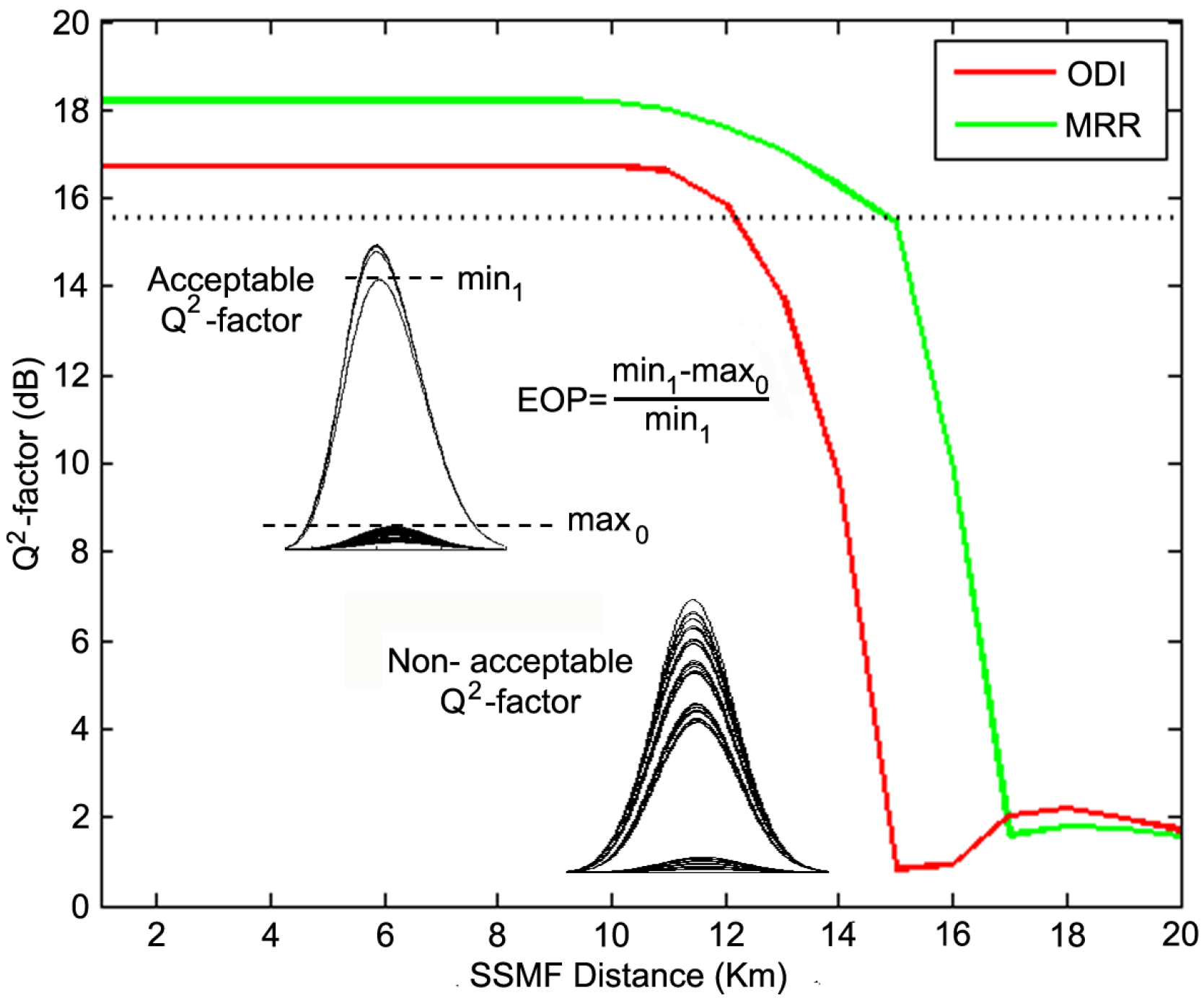
(iii) The MRR allows the amplified signal to propagate over a longer distance of SSMF without dispersion compensation than the ODI. This is shown in Figure 11, which has been obtained by modeling the SSMF of typical attenuation coefficient 0.2 dB/km and dispersion parameter 17 ps/nm/km by its low-pass equivalent field transfer function [63]. From this figure, it can be seen first that subject to chromatic dispersion, the maximum SSMF length is reduced to around 20 km, as calculated from [64] (cf. Equation (1)) for intensity-modulated data pulses of a 100-ps repetition period and 27% duty cycle. Then, looking for the transmission range for which the -factor is acceptable, we observe that the amplified signal can travel up to 12 km with the ODI, while this span is extended to 15 km with the MRR. This length difference may seem small, but nevertheless, it corresponds to the reach of real short-haul fiber interconnection links and networks [65]. Moreover, the -factor is well over its lower permissible bound for the MRR, while it is much closer to the borderline for the ODI, across the SSMF distance over which this metric remains acceptable for both filters. These observations can be interpreted by referring to the instantaneous frequency deviation, i.e., chirp, which inevitably accompanies a signal when directly amplified in an SOA [26]. More specifically, suppressing the SOA pattern effect by means of optical notch filtering relies on compensating for the chirp components, which are induced due to the irregular SOA gain variation by the optical excitation, and converting them into amplitude changes that counteract those after the SOA ([27], cf. Figure 4.18). Still, it is not possible to fully eliminate the SPM-induced negative-magnitude chirp components, which are directly associated with the SOA pattern effect, but only reduce the variations of their uneven peaks [31]. By calculating the maximum chirp variation, which occurs in the transition between the last ‘0’ in a run of spaces and the ‘1’ that immediately follows, we can extract the chirp parameter at the filters’ output similarly to the numerical procedure described in [66]. The value of this parameter is positive and is larger for the ODI than for the MRR. In the presence of anomalous chromatic dispersion, this fact subsequently affects the pulse width of the chirped signal at the filters’ output [52]. Thus, after a short distance zone of pulse compression, pulse broadening occurs, which is more significant for the ODI than for the MRR. This is reflected in the -factor, which is smaller for the ODI and becomes worsened after propagation in a shorter SSMF length (which is also smaller than that calculated from [64] (cf. Equation (1)) for the chirped-free signal case). The obtained results are further supported by the so-called pseudo-eye diagrams (PEDs) [67], which are displayed at different points of the -factor curves. Thus, both MRR and ODI restore the form of the PED, which has severely been degenerated into asymmetric sub-envelopes at the SOA output. This improvement is further quantified by the degree of eye opening (EOP) [68], which is higher for the MRR than for the ODI, i.e., 91% vs. 87%, respectively, for transmission in the same fiber length of 12 km.
The above improvements can be attributed to the different shape of the MRR and ODI transfer functions [69]. This difference affects the efficiency of the frequency-to-amplitude conversion mechanism, which is essential for suppressing the SOA pattern effect [44] and thus makes the MRR and ODI perform differently when employed as notch filters. Moreover, the comparatively better performance of the MRR can be justified from a qualitative standpoint by noting that the MRR exhibits higher wavelength sensitivity than the ODI. In fact, for the MRR, this quantity is determined, and hence enhanced, by the finesse [70], which is a function of the coupling coefficient and internal loss [27] and accordingly can be flexibly adjusted. In contrast, the finesse of the ODI is very small, i.e., it equals only two [52], and therefore is fixed so that the design freedom is very limited. Physically, this happens due to the different operating nature of the ODI and MRR, since in the former, only two constituents of the input field interfere to produce an output, whilst in the MRR, the field experiences multiple circulations before it leaves the resonant cavity [71]. Since in the first case, the interfering paths are feeding forward, while in the second case there is a recirculating, feedback delay path, this difference, which is reflected on the polynomial form of the respective transfer functions, can also be expressed in signal processing terms. Accordingly, the ODI and MRR can be used not only as notch filters, but in general as finite impulse response (FIR) and infinite impulse response (IIR) filters, respectively [72]. FIR filters that exploit MRRs are also possible if sophisticated designs based on the combination of multiple such elements are adopted [73].
The values obtained for the employed performance metrics have been gathered in Table 1.
6. ODI vs. MRR Qualitative Comparison
The key characteristics that the ODI- and MRR-based notch filters must exhibit in order to mitigate the SOA pattern effect can be further assessed in a qualitative manner by considering the following functional and technological issues:
- (a)
- FSR:
The FSR of both filters can conveniently lie within the SOA wide gain spectrum enabled through suitable adjustment of the SOA active layer material composition [1]. For the ODI, the FSR can be adjusted either statically, by fixing the path length imbalance, which can be of the order of um, between the ODI upper and lower arms, or dynamically, by using an optical delay line [32]. In the first case, a precise construction is required, but which is compensated by the reduction in footprint [74], while in the second case, a wide range of relative delays can be offered with fine resolution at the expense of a more bulky configuration [29]. For the MRR, the FSR can be readily set by choosing the MRR radius, which can be down to the micrometer scale using high index contrast waveguide materials [40,75]. This offers the comparative benefit of ultra-compact total size at the expense of resorting to elaborate and delicate microelectronic fabrication processes, which detracts from the global use of the specific scheme.
- (b)
- Detuning:
The position of the notches relative to the input data carrier wavelength can be practically adjusted by exploiting effects such as thermo-optic. For this purpose, either active phase shifters are used to control the phase bias in the ODI [58] or electrical heaters in the direct vicinity of the MRR to spectrally shift its resonance [75]. This method is particularly efficient for materials of large positive thermo-optic coefficients, such as silicon, since the required amount of detuning across the FSR can be achieved with a power supply of the order of mWs for both filters. On the other hand, the need for precise detuning is inherently more demanding for the ODI than for the MRR. This happens due to the different way by which the amount of phase shift required for efficiently suppressing the SOA pattern effect is obtained. Thus, for the ODI, this amount is acquired through one-way interference of a pair of delayed signal copies, while for the MRR through periodic round-trips and resonant enhancement. Accordingly, the ODI operation is more sensitive to deviations from the condition of destructive interference, which must be tightly satisfied at its cross-wise output port [30], thus requiring special design [76,77].
- (c)
- PNCR:
For the ODI the optimum PNCR can be achieved by adjusting the power splitting ratios of the optical couplers that form its two branches to be as symmetric as possible, i.e., as close as possible to 3 dB [78]. In practice, in order to ensure a PNCR over 20 dB, the deviation from the perfect 3-dB splitting ratio must be kept within 10% [29]. This tolerance is satisfiable with the coupling technology employed both in the fiber [79] and the waveguide [80] versions of the ODI.
Similarly, for the MRR, it is necessary to satisfy the condition of critical coupling, where the MRR field transmission coefficient, r, and amplitude attenuation factor, l, are equal while tending to unity [40]. In effect, the PNCR exceeds 20 dB even if this matching is less than 3% perfect [81]. The required matching can be accomplished by means of electrically-driven micro-electromechanical system (MEMS) microactuators, which control the gap by deforming the straight waveguide against the ring [82]. The ring, waveguide and MEMS actuators can be patterned with standard optical lithography, thus rendering the fabrication of the whole system technologically feasible.
- (d)
- Temperature sensitivity:
Although the strong thermo-optic effect of materials used as a platform for constructing the considered filters allows one to efficiently tune them, it is also responsible for making them prone to temperature fluctuations [83]. This susceptibility may cause the bias point of the ODI and the resonance wavelength of the MRR to drift, which in turn could affect the process of suppressing the red-shifted spectral components without significantly impairing the input data carrier and eventually leading to temperature-dependent performance degradation. Although it was numerically verified above that the MRR is, by its principle of operation, more tolerant to detuning offsets than the ODI, still, special care must additionally be taken in order to enhance the resilience of both schemes to possible temperature changes while at the same time achieving this goal in an energy-efficient manner. To this aim, it has been identified [83] that while athermal operation of the ODI is possible without any extra energy consumption, there is no efficient passive solution to the problem for the MRR, as well. Furthermore, the exploitation of negative thermo-optic materials that could resolve the thermo-optic issue in a straightforward manner faces challenges with regard to compatibility with standard CMOS technology and is the subject of intense research.
- (e)
- Integration potential:
Both schemes are amenable to integration, which is highly desirable for keeping size and IL small while enabling interconnection even at a small scale level. Thus, both are compatible with planar light wave technology and can be co-packaged with the SOA in the same module in a monolithic (ODI) [80] or hybrid (MRR) [67,84] platform. Especially, the capability for co-packaging is rather crucial towards compensating for the reduction in the amplified signal level due to notch filtering and hence for extending transmission reach. Since the MRR can be made more compact than the ODI [83,85], the use of the former could be favored for mitigating the SOA pattern effect in applications where space availability is critical, as in the transmitter side for power boosting, especially of multiple wavelength outputs, or the receiver end for power preamplification, or within intra-data center optical links [85]. On the other hand, it should be noted that both filters are compatible with standard CMOS (complementary metal-oxide-semiconductor) processing in silicon photonics platform [85,86] and hence can leverage the benefits that accompany this mature fabrication technology.
- (f)
- Multi-wavelength operation:
Both filters can mitigate the SOA pattern effect induced on wavelength-division-multiplexed (WDM) data inputs, for all channels simultaneously [87]. The specific potential is enabled by the periodic spectral response of these filters and can be exploited provided that the center wavelengths of the different input data are spaced apart by integer multiples of the FSR [21,58]. In this case, the amplitude equalization can be realized by means of a single such optical notch filter, which is attractive from an economical point of view, since the cost of using the device can be shared among the multiple served data inputs and remain affordable with the increase of channel count [62].
Furthermore, the two types of filters can be discriminated, with regard to their efficiency, to enhance the amplitude uniformity of multiple SOA amplified data-carrying channels, by the amount of the achieved FSR, which is compared against the wavelength separation between adjacent channels in real deployed WDM communication systems. Thus, for the ODI, the FSR that corresponds to a relative delay of ∼10 ps between its two arms is almost the standardized dense WDM grid spacing of 0.8 nm at around a 1550-nm carrier wavelength. On the contrary, the MRR μm radial size results in an FSR that is an order of magnitude higher and accordingly more suitable for coarse WDM purposes. Another option is to cascade several MRRs of different radii along the same waveguide bus [88]. This allows one to accommodate more data wavelengths impaired by the SOA pattern effect and with a more dense spacing than for a single MRR [33], at the expense of a larger footprint and a more complex configuration. On the other hand, in WDM systems of some given interchannel spacing and spectral width, a single MRR can support numerous channels in a much more flexible manner than a single ODI. In fact, this capability critically depends on one filter’s finesse, which, as previously mentioned, can be flexibly adjusted for the MRR, whereas it is very low and fixed for the ODI. Furthermore, the sharper spectral selectivity of the MRR allows the latter to better handle variations in the channel positions and compensate for possible misalignments against notches. This further allows one to use uncooled, i.e., non-temperature-controlled, single-mode lasers, which is an attractive feature from a cost and operational perspective [8]. In contrast, these functional requirements can be met with the ODI only if multiple ODI stages are concatenated [52], which, along with the aforementioned inevitable compromises associated with the employment of chains of filters, comes at the additional cost of extra losses.
- (g)
- Tunability:
The tunability of each type of filter can be assessed against bandwidth tunability and wavelength tunability [89]. For the first ability, we can calculate its minimum, which can be done in a straightforward manner by using the analytic formulas that quantify it. These are given from [52] for the ODI and [75]. Recall now that in order to prevent the filtering action that suppresses the SOA pattern effect on the data pulses from distorting the latter, the ODI delay should not exceed 10 ps [31], while the MRR radius should not be larger than 42 um [33]. Then, substituting these maximum values together with nm, and in the above expressions of the FWHM, it can be found that nm and nm. For the second ability, on the other hand, we have shown from Figure 10 that the wavelength offset of the MRR is allowed to be larger than that of the ODI while maintaining an acceptable -factor. Thus, in both cases, the numerically-obtained numbers suggest that the MRR filter is better tunable for the target application of SOA pattern effect compensation.
Table 2 summarizes the qualitative comparison of the MRR and ODI key characteristics. Note that this comparison is not absolute in the sense that each filter has its own special features, which may render it more suitable than the other for exploitation in SOA direct amplification applications with a suppressed pattern effect.
7. Conclusions
In conclusion, we have presented a theoretical analysis and benchmarking of two basic optical notch filters employed to compensate for the pattern effect that manifests in an SOA due to the irregular perturbation of the SOA gain dynamics by a directly-amplified data-modulated optical signal. After following a rational procedure based on the satisfaction of signal amplitude equalization conditions, we extracted values of the critical operating parameters, which enable a fair comparison of these filters through evaluating them against appropriately-adopted figures-of-merit. In this manner, we have specified the points where the considered filters perform better due to their different principles of operation and associated spectral responses. The obtained results denote that, with the exception of larger amplitude modulation, which however is well compensated by the other comparative realized improvements, the MRR outperforms the ODI in most employed metrics. This conclusion is further supported by the comparison made between the filters from a functional and technical side. In fact, the MRR exhibits several attractive key characteristics, which, along with its capability to confront the SOA pattern effect, allows it to favorably compete against the well-established ODI. This fact constructively broadens the technological options that are available for addressing the target problem. Furthermore, it indicates that, since there is no absolute criterion for preferring one filter to the other, making a selection should be done in such a way so that it best suits the particular needs of a light wave link or network where SOA direct amplification with a suppressed pattern effect is essential. To this end, each filter should judiciously be exploited while making the necessary trade-offs according to its inherent performance advantages and disadvantages.
Author Contributions
Zoe V. Rizou conducted the simulation and interpreted the obtained results; Kyriakos E. Zoiros conceived the initial idea and wrote the paper; Antonios Hatziefremidis reviewed the results and the manuscript.
Conflicts of Interest
The authors declare no conflict of interest.
References
- Zimmerman, D.R.; Spiekman, L.H. Amplifiers for the masses: EDFA, EDWA, and SOA amplets for metro and access applications. J. Lightwave Technol. 2004, 22, 63–70. [Google Scholar] [CrossRef]
- Bonk, R.; Schmuck, H.; Poehlmann, W.; Pfeiffer, T. Beneficial OLT transmitter and receiver concepts for NG-PON2 using semiconductor optical amplifiers. J. Opt. Commun. Netw. 2015, 7, A467–A473. [Google Scholar] [CrossRef]
- Connelly, M.J. Semiconductor Optical Amplifiers; Kluwer Academic Publishers: Dordrecht, The Netherlands, 2002; Chapter 6. [Google Scholar]
- Mørk, J.; Nielsen, M.L.; Berg, T.W. The dynamics of semiconductor optical amplifiers: Modeling and applications. Opt. Photonics News 2003, 14, 42–48. [Google Scholar] [CrossRef]
- Kamelian. Applications Note No. 0001 “Semiconductor Optical Amplifiers (SOAs) as Power Boosters” and No. 0002 “Semiconductor Optical Amplifiers (SOAs) as Pre-Amplifiers”. Available online: http://www.kamelian.com (accessed on 12 July 2017).
- Spiekman, L.H.; Wiesenfeld, J.; Gnauck, A.; Garrett, L.; Van Den Hoven, G.; Van Dongen, T.; Sander-Jochem, M.; Binsma, J. Transmission of 8 DWDM channels at 20 Gb/s over 160 Km of standard fiber using a cascade of semiconductor optical amplifiers. IEEE Photonics Technol. Lett. 2000, 12, 717–719. [Google Scholar] [CrossRef]
- Udvary, E.; Berceli, T. Semiconductor optical amplifier for detection function in radio over fiber systems. J. Lightwave Technol. 2008, 26, 2563–2570. [Google Scholar] [CrossRef]
- Porto, S.; Antony, C.; Ossieur, P.; Townsend, P.D. An upstream reach-extender for 10 Gb/s PON applications based on an optimized semiconductor amplifier cascade. Opt. Express 2012, 20, 186–191. [Google Scholar] [CrossRef] [PubMed]
- Yiannopoulos, K.; Sagias, N.C.; Boucouvalas, A.C. Fade mitigation based on semiconductor optical amplifiers. J. Lightwave Technol. 2013, 31, 3621–3630. [Google Scholar] [CrossRef]
- Miao, W.; Luo, J.; Di Lucente, S.; Dorren, H.; Calabretta, N. Novel flat datacenter network architecture based on scalable and flow-controlled optical switch system. Opt. Express 2014, 22, 2465–2472. [Google Scholar] [CrossRef]
- Schmuck, H.; Bonk, R.; Poehlmann, W.; Haslach, C.; Kuebart, W.; Karnick, D.; Meyer, J.; Fritzsche, D.; Weis, E.; Becker, J.; et al. Demonstration of an SOA-assisted open metro-access infrastructure for heterogeneous services. Opt. Express 2014, 22, 737–748. [Google Scholar] [CrossRef]
- Pato, S.V.; Meleiro, R.; Fonseca, D.; Andre, P.; Monteiro, P.; Silva, H. All-optical burst-mode power equalizer based on cascaded SOAs for 10-Gb/s EPONs. IEEE Photonics Technol. Lett. 2008, 20, 2078–2080. [Google Scholar] [CrossRef]
- Manning, R.; Ellis, A.; Poustie, A.; Blow, K. Semiconductor laser amplifiers for ultrafast all-optical signal processing. J. Opt. Soc. Am. B 1997, 14, 3204–3216. [Google Scholar] [CrossRef]
- Zoiros, K.; Chasioti, R.; Koukourlis, C.; Houbavlis, T. On the output characteristics of a semiconductor optical amplifier driven by an ultrafast optical time division multiplexing pulse train. Optik 2007, 118, 134–146. [Google Scholar] [CrossRef]
- Rizou, Z.V.; Zoiros, K.E.; Hatziefremidis, A.; Connelly, M.J. Design analysis and performance optimization of a Lyot filter for semiconductor optical amplifier pattern effect suppression. J. Sel. Top. Quantum Electron. 2013, 19, 1–9. [Google Scholar] [CrossRef]
- Bonk, R.; Huber, G.; Vallaitis, T.; Koenig, S.; Schmogrow, R.; Hillerkuss, D.; Brenot, R.; Lelarge, F.; Duan, G.H.; Sygletos, S.; et al. Linear semiconductor optical amplifiers for amplification of advanced modulation formats. Opt. Express 2012, 20, 9657–9672. [Google Scholar] [CrossRef] [PubMed]
- Bogoni, A.; Potì, L.; Ghelfi, P.; Scaffardi, M.; Porzi, C.; Ponzini, F.; Meloni, G.; Berrettini, G.; Malacarne, A.; Prati, G. OTDM-based optical communications networks at 160 Gbit/s and beyond. Opt. Fiber Technol. 2007, 13, 1–12. [Google Scholar] [CrossRef]
- Winzer, P.J.; Essiambre, R.J. Advanced modulation formats for high-capacity optical transport networks. J. Lightwave Technol. 2006, 24, 4711–4728. [Google Scholar] [CrossRef]
- Mecozzi, A.; Mørk, J. Saturation induced by picosecond pulses in semiconductor optical amplifiers. J. Opt. Soc. Am. B 1997, 14, 761–770. [Google Scholar] [CrossRef]
- Inoue, K. Optical filtering technique to suppress waveform distortion induced in a gain-saturated semiconductor optical amplifier. Electron. Lett. 1997, 33, 885–886. [Google Scholar] [CrossRef]
- Watanabe, T.; Yasaka, H.; Sakaida, N.; Koga, M. Waveform shaping of chirp-controlled signal by semiconductor optical amplifier using Mach-Zehnder frequency discriminator. IEEE Photonics Technol. Lett. 1998, 10, 1422–1424. [Google Scholar] [CrossRef]
- Yu, J.; Jeppesen, P. Increasing input power dynamic range of SOA by shifting the transparent wavelength of tunable optical filter. J. Lightwave Technol. 2001, 19, 1316–1325. [Google Scholar] [Green Version]
- Wong, C.; Tsang, H. Reduction of bit-pattern dependent errors from a semiconductor optical amplifier using an optical delay interferometer. Opt. Commun. 2004, 232, 245–249. [Google Scholar] [CrossRef]
- Dong, J.; Zhang, X.; Wang, F.; Hong, W.; Huang, D. Experimental study of SOA-based NRZ-to-PRZ conversion and distortion elimination of amplified NRZ signal using spectral filtering. Opt. Commun. 2008, 281, 5618–5624. [Google Scholar] [CrossRef]
- Hussain, K.; Pradhan, R.; Datta, P. Patterning characteristics and its alleviation in high bit-rate amplification of bulk semiconductor optical amplifier. Opt. Quantum Electron. 2010, 42, 29–43. [Google Scholar] [CrossRef]
- Agrawal, G.P.; Olsson, N.A. Self-phase modulation and spectral broadening of optical pulses in semiconductor laser amplifiers. IEEE J. Quantum Electron. 1989, 25, 2297–2306. [Google Scholar] [CrossRef]
- Wang, J. Pattern Effect Mitigation Techniques for All-Optical Wavelength Converters Based on SOAs. Ph.D. Thesis, Karlsruhe Institute of Technology, Karlsruhe, Germany, 2008. [Google Scholar]
- Zoiros, K.E.; O’Riordan, C.; Connelly, M.J. Semiconductor optical amplifier pattern effect suppression using a birefringent fiber loop. IEEE Photonics Technol. Lett. 2010, 22, 221–223. [Google Scholar] [CrossRef]
- Rizou, Z.; Zoiros, K.; Hatziefremidis, A.; Connelly, M. Performance tolerance analysis of birefringent fiber loop for semiconductor optical amplifier pattern effect suppression. Appl. Phys. B Lasers Opt. 2015, 119, 247–257. [Google Scholar] [CrossRef]
- Zoiros, K.E.; Siarkos, T.; Koukourlis, C.S. Theoretical analysis of pattern effect suppression in semiconductor optical amplifier utilizing optical delay interferometer. Opt. Commun. 2008, 281, 3648–3657. [Google Scholar] [CrossRef]
- Zoiros, K.E.; Rizou, Z.V.; Connelly, M.J. On the compensation of chirp induced from semiconductor optical amplifier on RZ data using optical delay interferometer. Opt. Commun. 2011, 284, 3539–3547. [Google Scholar] [CrossRef]
- Zoiros, K.E.; Janer, C.L.; Connelly, M.J. Semiconductor optical amplifier pattern effect suppression for return-to-zero data using an optical delay interferometer. Opt. Eng. 2010, 49, 1–4. [Google Scholar]
- Rizou, Z.; Zoiros, K.; Hatziefremidis, A. Semiconductor optical amplifier pattern effect suppression with passive single microring resonator-based notch filter. Opt. Commun. 2014, 329, 206–213. [Google Scholar] [CrossRef]
- Katz, O.; Malka, D. Design of novel SOI 1 × 4 optical power splitter using seven horizontally slotted waveguides. Photonics Nanostruct. 2017, 25, 9–13. [Google Scholar] [CrossRef]
- Malka, D.; Peled, A. Power splitting of 1 × 16 in multicore photonic crystal fibers. Appl. Surf. Sci. 2017, 417, 34–39. [Google Scholar] [CrossRef]
- Ben Zaken, B.B.; Zanzury, T.; Malka, D. An 8-channel wavelength MMI demultiplexer in slot waveguide structures. Materials 2016, 9, 881. [Google Scholar] [CrossRef]
- Malka, D.; Sintov, Y.; Zalevsky, Z. Design of a 1 × 4 silicon-alumina wavelength demultiplexer based on multimode interference in slot waveguide structures. J. Opt. 2015, 17, 125702. [Google Scholar] [CrossRef]
- Malka, D.; Sintov, Y.; Zalevsky, Z. Fiber-laser monolithic coherent beam combiner based on multicore photonic crystal fiber. Opt. Eng. 2015, 54, 011007. [Google Scholar] [CrossRef]
- Wong, C.; Tsang, H. Filtering directly modulated laser diode pulses with a Mach-Zehnder optical delay interferometer. Electron. Lett. 2004, 40, 938–940. [Google Scholar] [CrossRef]
- Rabus, D.G. Integrated Ring Resonators: The Compendium; Spring: Berlin, Germany, 2007. [Google Scholar]
- Sumetsky, M. Optimization of resonant optical sensors. Opt. Express 2007, 15, 17449–17457. [Google Scholar] [CrossRef] [PubMed]
- Ruege, A.C. Electro-Optic Ring Resonators in Integrated Optics for Miniature Electric Field Sensors. Ph.D. Thesis, The Ohio State University, Columbus, OH, USA, 2001. [Google Scholar]
- Nielsen, M.L.; Mørk, J. Bandwidth enhancement of SOA-based switches using optical filtering: Theory and experimental verification. Opt. Express 2006, 14, 1260–1265. [Google Scholar] [CrossRef] [PubMed]
- Udvary, E. Off-set filtering effect in SOA based optical access network. Radioengineering 2016, 25, 26–33. [Google Scholar] [CrossRef]
- Yu, H.Y.; Mahgerefteh, D.; Cho, P.S.; Goldhar, J. Optimization of the frequency response of a semiconductor optical amplifier wavelength converter using a fiber Bragg grating. J. Lightwave Technol. 1999, 17, 308–315. [Google Scholar]
- Nielsen, M.L.; Mørk, J.; Suzuki, R.; Sakaguchi, J.; Ueno, Y. Theoretical and experimental study of fundamental differences in the noise suppression of high-speed SOA-based all-optical switches. Opt. Express 2005, 13, 5080–5086. [Google Scholar] [CrossRef] [PubMed]
- Nielsen, M.L. Experimental and Theoretical Investigation of Semiconductor Optical Amplifier (SOA) Based All-Optical Switches. Ph.D. Thesis, Technical University of Denmark, Kongens Lyngby, Denmark, 2004. [Google Scholar]
- Rizou, Z.V.; Zoiros, K.E. Performance analysis and improvement of semiconductor optical amplifier direct modulation with assistance of microring resonator notch filter. Opt. Quantum Electron. 2017, 3, 1–21. [Google Scholar] [CrossRef]
- Vardakas, J.S.; Zoiros, K.E. Performance investigation of all-optical clock recovery circuit based on Fabry-Pérot filter and semiconductor optical amplifier assisted Sagnac switch. Opt. Eng. 2007, 46, 1–21. [Google Scholar]
- Gutiérrez-Castrejón, R.; Filios, A. Pattern-effect reduction using a cross-gain modulated holding beam in semiconductor optical in-line amplifier. J. Lightwave Technol. 2006, 24, 4912–4917. [Google Scholar] [CrossRef]
- Yan, S.; Zhang, Y.; Dong, J.; Zheng, A.; Liao, S.; Zhou, H.; Wu, Z.; Xia, J.; Zhang, X. Operation bandwidth optimization of photonic differentiators. Opt. Express 2015, 23, 18925–18936. [Google Scholar] [CrossRef] [PubMed]
- Agrawal, G.P. Fiber-Optic Communication Systems, 3rd ed.; Wiley: New York, NY, USA, 2002. [Google Scholar]
- Bonk, R.; Vallaitis, T.; Guetlein, J.; Meuer, C.; Schmeckebier, H.; Bimberg, D.; Koos, C.; Freude, W.; Leuthold, J. The input power dynamic range of a semiconductor optical amplifier and its relevance for access network applications. IEEE Photonics J. 2011, 3, 1039–1053. [Google Scholar] [CrossRef]
- Vacondio, F.; Ghazisaeidi, A.; Bononi, A.; Rusch, L.A. Low-complexity compensation of SOA nonlinearity for single-channel PSK and OOK. J. Lightwave Technol. 2010, 28, 277–288. [Google Scholar] [CrossRef]
- Xu, J.; Zhang, X.; Mørk, J. Investigation of patterning effects in ultrafast SOA-based optical switches. IEEE J. Quantum Electron. 2010, 46, 87–94. [Google Scholar] [CrossRef]
- MacWilliams, F.J.; Sloane, N.J. Pseudo-random sequences and arrays. Proc. IEEE 1976, 64, 1715–1729. [Google Scholar] [CrossRef]
- Singh, S.; Kaler, R. Transmission performance of 20 × 10 Gb/s WDM signals using cascaded optimized SOAs with OOK and DPSK modulation formats. Opt. Commun. 2006, 266, 100–110. [Google Scholar] [CrossRef]
- Bhardwaj, A.; Doerr, C.R.; Chandrasekhar, S.; Stulz, L.W. Reduction of nonlinear distortion from a semiconductor optical amplifier using an optical equalizer. IEEE Photonics Technol. Lett. 2004, 16, 921–923. [Google Scholar] [CrossRef]
- Niehusmann, J.; Vörckel, A.; Bolivar, P.H.; Wahlbrink, T.; Henschel, W.; Kurz, H. Ultrahigh-quality-factor silicon-on-insulator microring resonator. Opt. Lett. 2004, 29, 2861–2863. [Google Scholar] [CrossRef] [PubMed]
- Fujiwara, M.; Imai, T.; Taguchi, K.; Suzuki, K.I.; Ishii, H.; Yoshimoto, N. Field trial of 100-km reach symmetric-rate 10 G-EPON system using automatic level controlled burst-mode SOAs. J. Lightwave Technol. 2013, 31, 634–640. [Google Scholar] [CrossRef]
- Porzi, C.; Kado, Y.; Shimizu, S.; Maruta, A.; Wada, N.; Bogoni, A.; Kitayama, K.I. Simple uplink SOA pattern effects compensation for reach-extended 10 G-EPONs. IEEE Photonics. Technol. Lett. 2014, 26, 165–168. [Google Scholar] [CrossRef]
- Kim, H. 10-Gb/s operation of RSOA using a delay interferometer. IEEE Photonics Technol. Lett. 2010, 22, 1379–1381. [Google Scholar] [CrossRef]
- Elrefaie, A.F.; Wagner, R.E.; Atlas, D.; Daut, D. Chromatic dispersion limitations in coherent light wave transmission systems. J. Lightwave Technol. 1988, 6, 704–709. [Google Scholar] [CrossRef]
- Forghieri, F.; Prucnal, P.; Tkach, R.; Chraplyvy, A.R. RZ versus NRZ in nonlinear WDM systems. IEEE Photonics Technol. Lett. 1997, 9, 1035–1037. [Google Scholar] [CrossRef]
- Levaufre, G.; Le Liepvre, A.; Jany, C.; Accard, A.; Kaspar, P.; Brenot, R.; Make, D.; Lelarge, F.; Olivier, S.; Malhouitre, S.; et al. Hybrid III-V/silicon tunable laser directly modulated at 10 Gbit/s for short reach/access networks. In Proceedings of the European Conference on Optical Communication, Cannes, France, 21–25 September 2014. [Google Scholar]
- Dubé-Demers, R.; LaRochelle, S.; Shi, W. Ultrafast pulse-amplitude modulation with a femtojoule silicon photonic modulator. Optica 2016, 3, 622–627. [Google Scholar] [CrossRef]
- Gutiérrez-Castrejón, R.; Occhi, L.; Schares, L.; Guekos, G. Recovery dynamics of cross-modulated beam phase in semiconductor amplifiers and applications to all-optical signal processing. Opt. Commun. 2001, 195, 167–177. [Google Scholar] [CrossRef]
- Gayen, D.K.; Chattopadhyay, T.; Zoiros, K.E. All-optical D flip-flop using single quantum-dot semiconductor optical amplifier assisted Mach-Zehnder interferometer. J. Comput. Electron. 2015, 14, 129–138. [Google Scholar] [CrossRef]
- Zhang, L.; Li, Y.; Song, M.; Beausoleil, R.G.; Willner, A.E. Data quality dependencies in microring-based DPSK transmitter and receiver. Opt. Express 2008, 16, 5739–5745. [Google Scholar] [CrossRef] [PubMed]
- Tazawa, H.; Kuo, Y.H.; Dunayevskiy, I.; Luo, J.; Jen, A.K.Y.; Fetterman, H.R.; Steier, W.H. Ring resonator-based electrooptic polymer traveling-wave modulator. J. Lightwave Technol. 2006, 24, 3514–3519. [Google Scholar] [CrossRef]
- Ye, T.; Cai, X. On power consumption of silicon-microring-based optical modulators. J. Lightwave Technol. 2010, 28, 1615–1623. [Google Scholar]
- Madsen, C.K.; Zhao, J.H. Optical Filter Design and Analysis: A Signal Processing Approach; John Wiley & Sons, Inc.: New York, NY, USA, 1999; pp. 1–5. [Google Scholar]
- Malka, D.; Cohen, M.; Turkiewicz, J.; Zalevsky, Z. Optical micro-multi-racetrack resonator filter based on SOI waveguides. Photonics Nanostruct. 2015, 16, 16–23. [Google Scholar] [CrossRef]
- Wu, Q.; Zhang, H.; Fu, X.; Yao, M. Spectral encoded photonic analog-to-digital converter based on cascaded unbalanced MZMs. IEEE Photonics Technol. Lett. 2009, 21, 224–226. [Google Scholar]
- Bogaerts, W.; De Heyn, P.; Van Vaerenbergh, T.; De Vos, K.; Kumar Selvaraja, S.; Claes, T.; Dumon, P.; Bienstman, P.; Van Thourhout, D.; Baets, R. Silicon microring resonators. Laser Photonics Rev. 2012, 6, 47–73. [Google Scholar] [CrossRef]
- Kim, T.Y.; Hanawa, M.; Kim, S.J.; Hann, S.; Kim, Y.H.; Han, W.T.; Park, C.S. Optical delay interferometer based on phase shifted fiber Bragg grating with optically controllable phase shifter. Opt. Express 2006, 14, 4250–4255. [Google Scholar] [CrossRef] [PubMed]
- Li, J.; Worms, K.; Maestle, R.; Hillerkuss, D.; Freude, W.; Leuthold, J. Free-space optical delay interferometer with tunable delay and phase. Opt. Express 2011, 19, 11654–11666. [Google Scholar] [CrossRef] [PubMed]
- Su, T.; Zhang, M.; Chen, X.; Zhang, Z.; Liu, M.; Liu, L.; Huang, S. Improved 10-Gbps uplink transmission in WDM-PON with RSOA-based colorless ONUs and MZI-based equalizers. Opt. Laser Technol. 2013, 51, 90–97. [Google Scholar] [CrossRef]
- Luo, Z.C.; Cao, W.J.; Luo, A.P.; Xu, W.C. Polarization-independent, multifunctional all-fiber comb filter using variable ratio coupler-based Mach-Zehnder interferometer. J. Lightwave Technol. 2012, 30, 1857–1862. [Google Scholar] [CrossRef]
- Bhardwaj, A.; Sauer, N.; Buhl, L.; Yang, W.; Zhang, L.; Neilson, D.T. An InP-based optical equalizer monolithically integrated with a semiconductor optical amplifier. IEEE Photonics Technol. Lett. 2007, 19, 1514–1516. [Google Scholar] [CrossRef]
- Absil, P.; Hryniewicz, J.; Little, B.; Wilson, R.; Joneckis, L.; Ho, P.T. Compact microring notch filters. IEEE Photonics Technol. Lett. 2000, 12, 398–400. [Google Scholar] [CrossRef]
- Lee, M.C.; Wu, M.C. MEMS-actuated microdisk resonators with variable power coupling ratios. IEEE Photonics Technol. Lett. 2005, 17, 1034–1036. [Google Scholar] [CrossRef]
- Zhou, Z.; Yin, B.; Deng, Q.; Li, X.; Cui, J. Lowering the energy consumption in silicon photonic devices and systems. Photonics Res. 2015, 3, B28–B46. [Google Scholar] [CrossRef]
- Kaspar, P.; Brenot, R.; Le Liepvre, A.; Accard, A.; Make, D.; Levaufre, G.; Girard, N.; Lelarge, F.; Duan, G.H.; Pavarelli, N.; et al. Packaged hybrid III-V/silicon SOA. In Proceedings of the European Conference on Optical Communication, Cannes, France, 21–25 September 2014. [Google Scholar]
- Li, Y.; Zhang, Y.; Zhang, L.; Poon, A.W. Silicon and hybrid silicon photonic devices for intra-datacenter applications: State of the art and perspectives. Photonics Res. 2015, 3, B10–B27. [Google Scholar] [CrossRef]
- Gunn, C. CMOS photonics for high-speed interconnects. IEEE Micro 2006, 26, 58–66. [Google Scholar] [CrossRef]
- Tan, H.N.; Matsuura, M.; Kishi, N. Enhancement of input power dynamic range for multiwavelength amplification and optical signal processing in a semiconductor optical amplifier using holding beam effect. J. Lightwave Technol. 2010, 28, 2593–2602. [Google Scholar] [CrossRef]
- Padmaraju, K.; Bergman, K. Resolving the thermal challenges for silicon microring resonator devices. Nanophotonics 2014, 3, 269–281. [Google Scholar] [CrossRef]
- Ding, Y.; Pu, M.; Liu, L.; Xu, J.; Peucheret, C.; Zhang, X.; Huang, D.; Ou, H. Bandwidth and wavelength-tunable optical bandpass filter based on silicon microring-MZI structure. Opt. Express 2011, 19, 6462–6470. [Google Scholar] [CrossRef] [PubMed]
Figure 1.
SOA direct amplification applications.

Figure 2.
Evolution of semiconductor optical amplifier (SOA) gain in response to data train input of repetition period, , such that pulses arrive faster than the interval available for SOA carrier replenishment, .
Figure 2.
Evolution of semiconductor optical amplifier (SOA) gain in response to data train input of repetition period, , such that pulses arrive faster than the interval available for SOA carrier replenishment, .

Figure 3.
Data amplification in SOA with pattern-dependent output distortion and compensation by optical notch filtering.
Figure 3.
Data amplification in SOA with pattern-dependent output distortion and compensation by optical notch filtering.
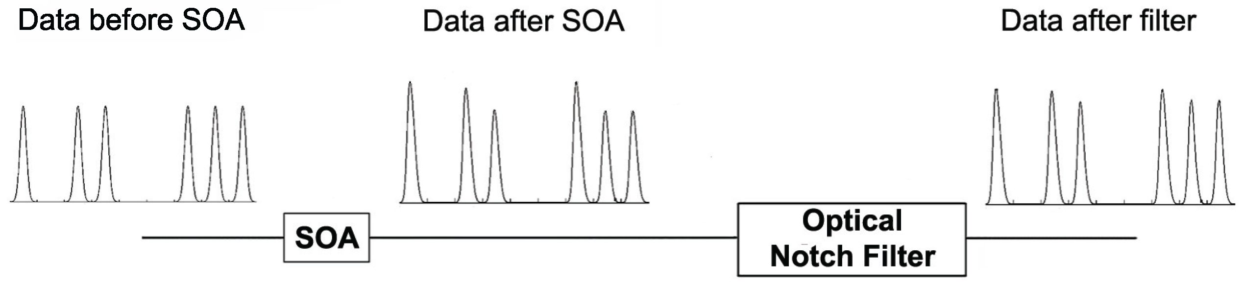
Figure 4.
(a) Optical delay interferometer (ODI) and (b) microring resonator (MRR) structure.
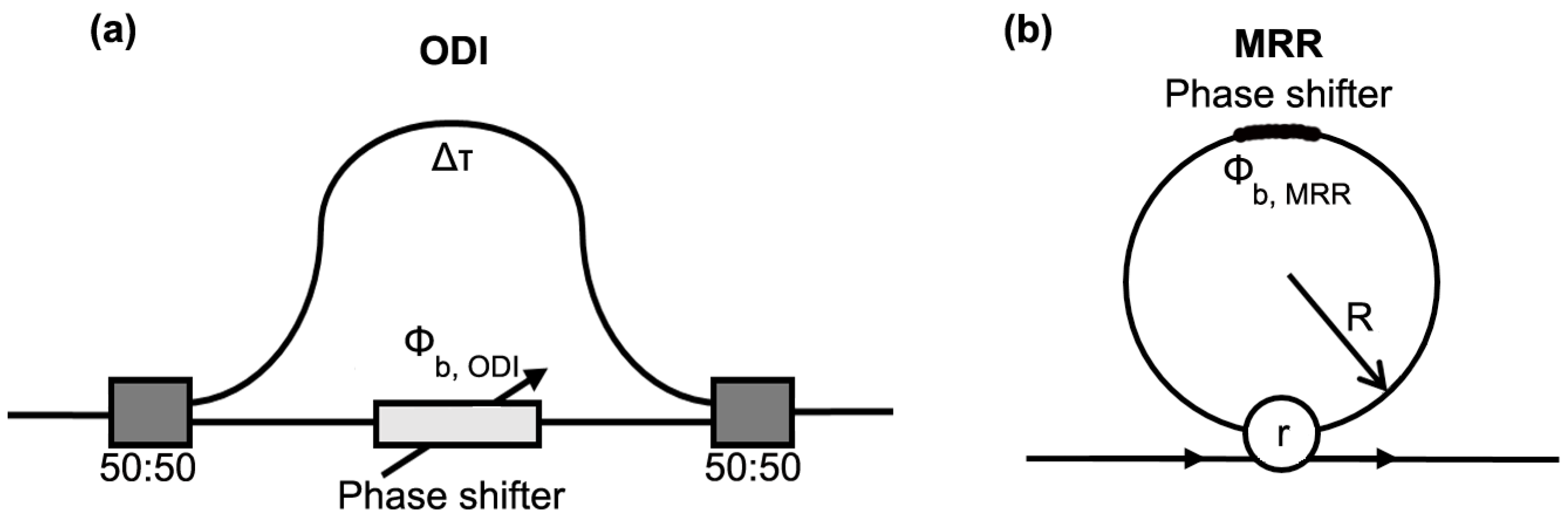
Figure 5.
ODI (red color) and MRR (green color) spectral response together with spectrum at SOA output (black color). The red-colored oblique line and the yellow-colored zones show the red-shifted spectral components, which are filtered by the ODI and MRR, respectively.
Figure 5.
ODI (red color) and MRR (green color) spectral response together with spectrum at SOA output (black color). The red-colored oblique line and the yellow-colored zones show the red-shifted spectral components, which are filtered by the ODI and MRR, respectively.

Figure 6.
Small-signal modulation response of SOA alone (black color) and with the assistance of ODI (red color) or MRR (green color). The dashed line denotes the 3-dB bandwidth level and the arrows the bandwidth extension achieved by the notch filters.
Figure 6.
Small-signal modulation response of SOA alone (black color) and with the assistance of ODI (red color) or MRR (green color). The dashed line denotes the 3-dB bandwidth level and the arrows the bandwidth extension achieved by the notch filters.

Figure 7.
Simulated temporal waveforms that contain maximum strings of ‘1’s and ‘0’s. (a) SOA input, (b) SOA output, (c) ODI output and (d) MRR output. The vertical arrows indicate the amplitude modulation ().
Figure 7.
Simulated temporal waveforms that contain maximum strings of ‘1’s and ‘0’s. (a) SOA input, (b) SOA output, (c) ODI output and (d) MRR output. The vertical arrows indicate the amplitude modulation ().

Figure 8.
(a) Profile of isolated data pulse at ODI (red color) and MRR (green color) output in comparison to SOA input (black color). (b) Corresponding chirp profile at ODI (red color) and MRR (green color).
Figure 8.
(a) Profile of isolated data pulse at ODI (red color) and MRR (green color) output in comparison to SOA input (black color). (b) Corresponding chirp profile at ODI (red color) and MRR (green color).

Figure 9.
-factor as a function of different peak input data powers for SOA alone (black color) and with the connection of ODI (red color) and MRR (green color). The horizontal dotted line denotes the lower limit set for the -factor. The vertical dashed lines define the different saturation regions: A, low; B, medium; C, deep.

Figure 10.
-factor for different detuning offset values for ODI (red color) and MRR (green color). The zero detuning refers to the case that the notch of the filters is located away from the data carrier by so many spectral units as defined in Figure 5.
Figure 10.
-factor for different detuning offset values for ODI (red color) and MRR (green color). The zero detuning refers to the case that the notch of the filters is located away from the data carrier by so many spectral units as defined in Figure 5.
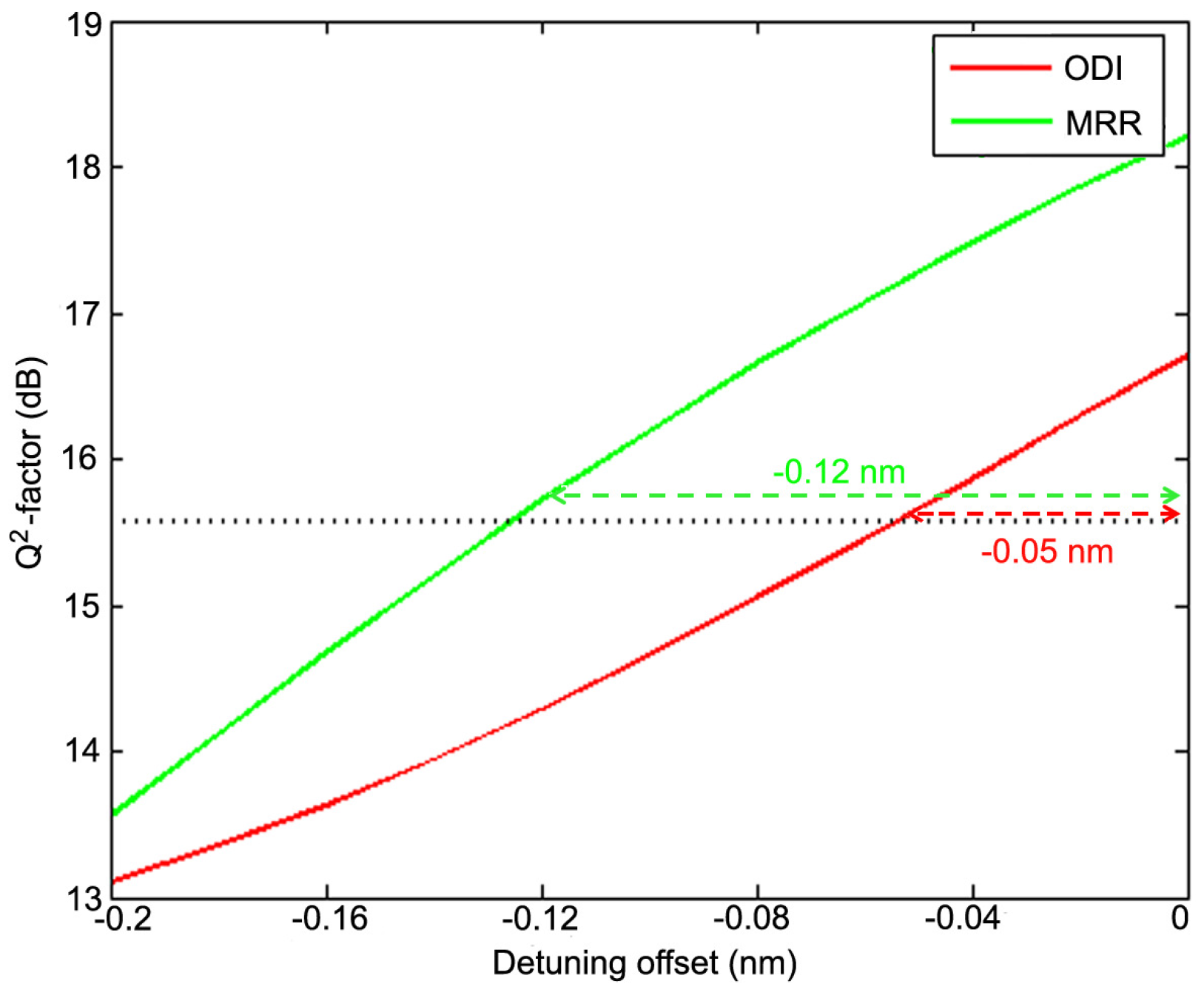
Figure 11.
-factor vs. standard single-mode fiber (SSMF) distance for ODI (red color) and MRR (green color). The horizontal dotted line denotes the lower limit set for the -factor.
Figure 11.
-factor vs. standard single-mode fiber (SSMF) distance for ODI (red color) and MRR (green color). The horizontal dotted line denotes the lower limit set for the -factor.


Table 1.
Values of employed performance metrics.
| Parameter | ODI | MRR |
|---|---|---|
| (dB) | 0.22 | 0.34 |
| (dB) | 3 | 2.78 |
| Net gain (dB) | 8.91 * | 12.13 |
| (%) | 93 | 97 |
| (dB) | 14 | 14 |
| (dB) | 1 | 2.87 |
| (negative) Detuning offset (nm) | 0.05 | 0.12 |
| SSMF distance (km) w/o dispersion compensation | 12 | 15 |
| EOP at 12 km (%) | 87 | 91 |
* 3 dB insertion losses included.
Table 2.
Qualitative comparison of MRR and ODI key characteristics.
| Characteristic | MRR | ODI | |
|---|---|---|---|
| Free Spectral Range (FSR) | Width | Coarse | Dense |
| Adjustment | Rather fine (radius) | Fine (path length imbalance) or bulky (optical delay line) | |
| Multi-wavelength Operation | Yes | Yes | |
| (i) ITU -Grid | Difficult for DWDM since it requires cascading; is compromised by increased footprint and complexity | Easy for DWDM | |
| (ii) fixed interchannel spacing and spectral width | Yes, easy with single MRR owing to high and controllable finesse | Yes, difficult due to low and fixed finesse | |
| (iii) handling of variations in channel positions | Yes, straightforward owing to sharp spectral selectivity | Yes, requires to concatenate multiple stages at the cost of increased complexity and insertion losses | |
| Detuning | Feasibility | Yes, thermo-optic effect with mWs/FSR | |
| Mechanism | Relaxed (periodic round-trips and resonant enhancement) | Tight (one-way interference) | |
| Precision | Normal | Demanding | |
| Tolerance | High | Medium | |
| Tunability | Yes, high | Yes, medium | |
| Peak-to-Notch Contrast Ratio (PNCR) | Magnitude | High (>20 dB) | |
| Operating Condition | Demanding (critical coupling) | Normal (branching couplers splitting ratio) | |
| Adjustment | Complicated (electrically driving MEMS to control gap between bus and ring) | Simple (varying power splitting ratio) | |
| Tolerance | Tight (matching of field transmission coefficient and amplitude attenuation factor within 3%) | Relaxed (Within 10% of 3-dB power splitting ratio) | |
| Temperature Sensitivity | Yes, high negative TOC material, but still not compatibility with standard CMOS technology | Yes, athermal operation without extra energy consumption | |
| Integration Potential | Compatibility with planar light wave technology | Yes | Yes |
| Co-packaging Platform with SOA | Yes (hybrid) | Yes (monolithic) | |
| Device | Size and footprint | Ultra-compact | Compact or bulk |
| Fabrication, (materials, techniques, processes) | Well-developed | Established | |
| CMOS Compatible | Yes | Yes | |
| Cost | Affordable (single channel amplification in SOA), Shared (multiple channel amplification in SOA) | ||
| Commercial availability | Yes, increasing | Yes, widespread | |
© 2017 by the authors. Licensee MDPI, Basel, Switzerland. This article is an open access article distributed under the terms and conditions of the Creative Commons Attribution (CC BY) license (http://creativecommons.org/licenses/by/4.0/).
Share and Cite
MDPI and ACS Style
Rizou, Z.V.; Zoiros, K.E.; Hatziefremidis, A. Comparison of Basic Notch Filters for Semiconductor Optical Amplifier Pattern Effect Mitigation. Appl. Sci. 2017, 7, 783. https://doi.org/10.3390/app7080783
AMA Style
Rizou ZV, Zoiros KE, Hatziefremidis A. Comparison of Basic Notch Filters for Semiconductor Optical Amplifier Pattern Effect Mitigation. Applied Sciences. 2017; 7(8):783. https://doi.org/10.3390/app7080783
Chicago/Turabian StyleRizou, Zoe V., Kyriakos E. Zoiros, and Antonios Hatziefremidis. 2017. "Comparison of Basic Notch Filters for Semiconductor Optical Amplifier Pattern Effect Mitigation" Applied Sciences 7, no. 8: 783. https://doi.org/10.3390/app7080783
Note that from the first issue of 2016, this journal uses article numbers instead of page numbers. See further details here.