Study on the Reliability of Sn50Pb49Sb1/Cu Solder Joints Subjected to γ-ray Irradiation


College of Materials Science and Technology, Nanjing University of Aeronautics and Astronautics, Nanjing 210016, China
*
Author to whom correspondence should be addressed.
Appl. Sci. 2018, 8(10), 1706; https://doi.org/10.3390/app8101706
Submission received: 24 August 2018
/
Revised: 10 September 2018
/
Accepted: 13 September 2018
/
Published: 20 September 2018
(This article belongs to the Special Issue Selected Papers from the NMJ2018)
Abstract
:Cosmic radiation has always been the most obvious barrier to planetary travels, especially in long-duration deep space exploration missions. Therefore, the reliability of satellite materials and the requirements of satellite miniaturization have received considerable attention. In this paper, the effect of γ-ray irradiation on the reliability of Sn50Pb49Sb1/Cu solder joints was investigated. It was found that the influence of γ-ray irradiation on the thickness and morphology of the intermetallic compound layer in Sn50Pb49Sb1/Cu was not obvious. However, the formation and growth of micro-voids and micro-cracks was observed in Pb-based solid solutions. Due to the Compton effect, the γ-ray photon could knock the electron out of its orbit, which created the energetic electron. The accumulation of dislocated atoms and lattice vacancies generated by energetic electrons could be the main factor that caused the formation of micro-voids and micro-cracks. The pull force of Sn50Pb49Sb1/Cu solder joints was reduced by 22% after being irradiated at the dose rate of 0.25 Gy(Si)/s for 960 h. Fractographic analysis showed that after irradiation, the fracture type of solder joints was still ductile but the ductility of the solder joints decreased with slightly inconspicuous dimples.
1. Introduction
Soldering plays an essential role in the manufacture of integrated circuits (IC), supporting the bonding of electrical conduction in integrated circuit interconnections between electrical components and printed circuit boards [1]. Due to a series of satellite processor failures induced by tin whiskers in solder joints, the reliability of electronic device solder joints has become a very important matter in electronic packaging in the past few decades [2,3]. With the trend of increasingly finer pins, greater demands have been placed on reliable solders with excellent resistance to specific service conditions, especially those of satellites.
Human beings have been dawn to the glamour of the universe and stars for thousands of years, and they are the basis of mythologies and legends, but the universe intermingles glamour and danger. With scientific development, many spacecrafts have been launched since the last century, attempting to understand the origin and evolution of the universe. Cosmic radiation induced by the sun, supernovae and other galaxies, is seen as a risk factor for in-orbit satellites [4,5]. Radiation particles including γ-ray photons, heavy ions and energetic electrons, could result in the performance drift and failure of electrical instruments, the majority of which is known as the total dose effect, single event effect and so on. According to the reports of National Aeronautics and Space Administration (NASA), the radiation dose rate of low earth-orbit satellites is usually 10–50 Gy(Si)/year, owing to the protection of the atmospheric layer and the magnetic field of the earth. However, for deep space satellites, the radiation dose may be remarkably increased due to the activity of the sun and other galaxies, such as solar storms and gamma ray bursts. Therefore, radiation-shielding components are currently applied to prevent in-orbit satellites from radiation damage [6]. Recently, a number of deep space exploration programs, including ExoMars of European Space Agency (ESA) and Solar Probe Plus of NASA, are in progress in order to explore vast, unknown areas of outer space. The developing trend for satellite miniaturization is proposed to meet the reliability and lightweight requirements of deep space exploration [7,8,9]. Therefore, investigations on the effect of cosmic radiation on satellite materials are utterly necessary for further research on the reliability and improvement of materials subjected to radiation, providing instructions and references for the fault-tolerant design of spacecrafts without radiation-shielding components.
Owing to its outstanding cryogenic performance, tin-lead (SnPb) solder is widely used in the aerospace industry, which is unrestricted by international legislation banning Pb application [10]. In this study, the microstructure and pull force of Sn50Pb49Sb1 solder joints subjected to γ-ray irradiation were investigated and the fracture morphologies of solder joints at various irradiation doses were analyzed.
2. Materials and Methods
2.1. Preparation of Specimens and Microstructure Observation
Sn50Pb49Sb1 solder alloy was prepared by smelting Sn, Cu and Sb metals with a purity of 99.9% in a vacuum resistant furnace and chilled to draw wire. The composition of the solder was tested by an inductively coupled plasma emission spectrometer (ICP-AES). Oxygen-free Cu was chosen as the substrate material, with the given size and cleaned surface. Sn50Pb49Sb1 solder alloy was soldered onto the Cu substrate by flux to prepare the solder joints. As the irradiation period was too long to carry out in situ observation, a few samples for microstructure observation were subjected to the following irradiation experiment. All samples were cut from the same solder joint to ensure the accuracy of the experiment. The microstructure of Sn50Pb49Sb1/Cu solder joints was observed using a scanning electron microscope (SEM) after grinding and polishing, and its chemical compositions were identified using an energy dispersive spectrometer (EDS).
2.2. Irradiation Treatment
The totally realistic simulation of a cosmic radiation environment, which is complicated and changing, is inaccessible on the earth. Therefore, 60Co-γ source is applied to partly simulate the cosmic radiation environment to test the radiation-resistance of devices and materials [11,12]. The absorbed dose is used to assess the irradiation dose that the specimens received. According to the Chinese Military Standard GJB 548B-2005 (test method military standard for microelectronics), all specimens were irradiated by 60Co-γ source from 0 h to 960 h at the dose rate of 0.25 Gy(Si)/s, to study the effect of γ-ray irradiation on Sn50Pb49Sb1/Cu solder joints. The dose rate was checked using a dosimeter before the irradiation experiment, and the radiation medium was air. Although the attenuation of rays in an air environment might be increased in comparison to a vacuum, the attenuation of gamma rays induced by air in this experiment was negligible due to the low attenuation coefficient of gamma photons in the air.
2.3. Pull Tests
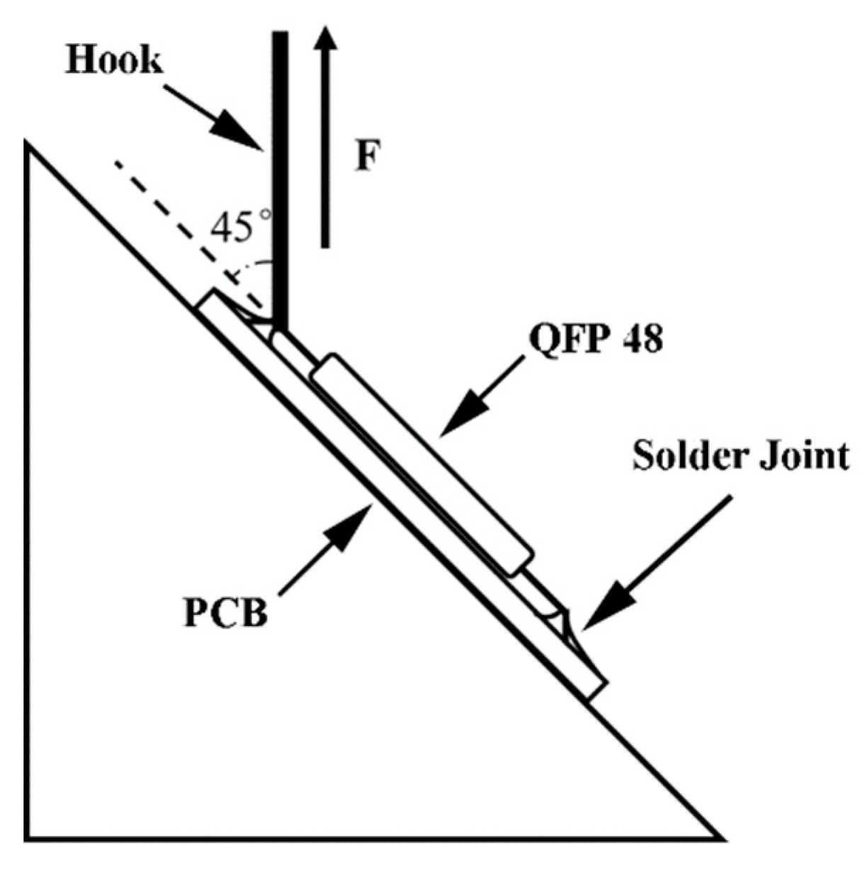
In order to investigate the strength evolution of Sn50Pb49Sb1/Cu solder joints subjected to γ-ray irradiation, quad flat packages (QFP48) were soldered onto printed circuit boards (PCB) by Sn50Pb49Sb1 solder alloy with flux. All QFP48 specimens were irradiated at various doses. Following this, pull tests were conducted with a joint strength tester (STR-1000), according to the Japanese Industry Standard JIS Z 3198-6 (Test Methods for Lead-free Solders-Part 6: Methods for 45 Degree Pull Test of Solder Joints on QFP Lead). The pin of QFP48 that was interconnected with the PCB by a Sn50Pb49Sb1 solder joint, was pulled up by a hook until the joint was snapped and the maximum pull force was collected to assess the strength of the solder joint, as shown in Figure 1. Pull tests of solder joints at the same parameter were conducted five times and the average value and standard deviation were taken to assess the strength evolution of the Sn50Pb49Sb1 solder joint after irradiation. After the pull tests, the fracture morphology of the solder joints was analyzed by SEM and EDS.
3. Results and Discussion
3.1. Microstructure
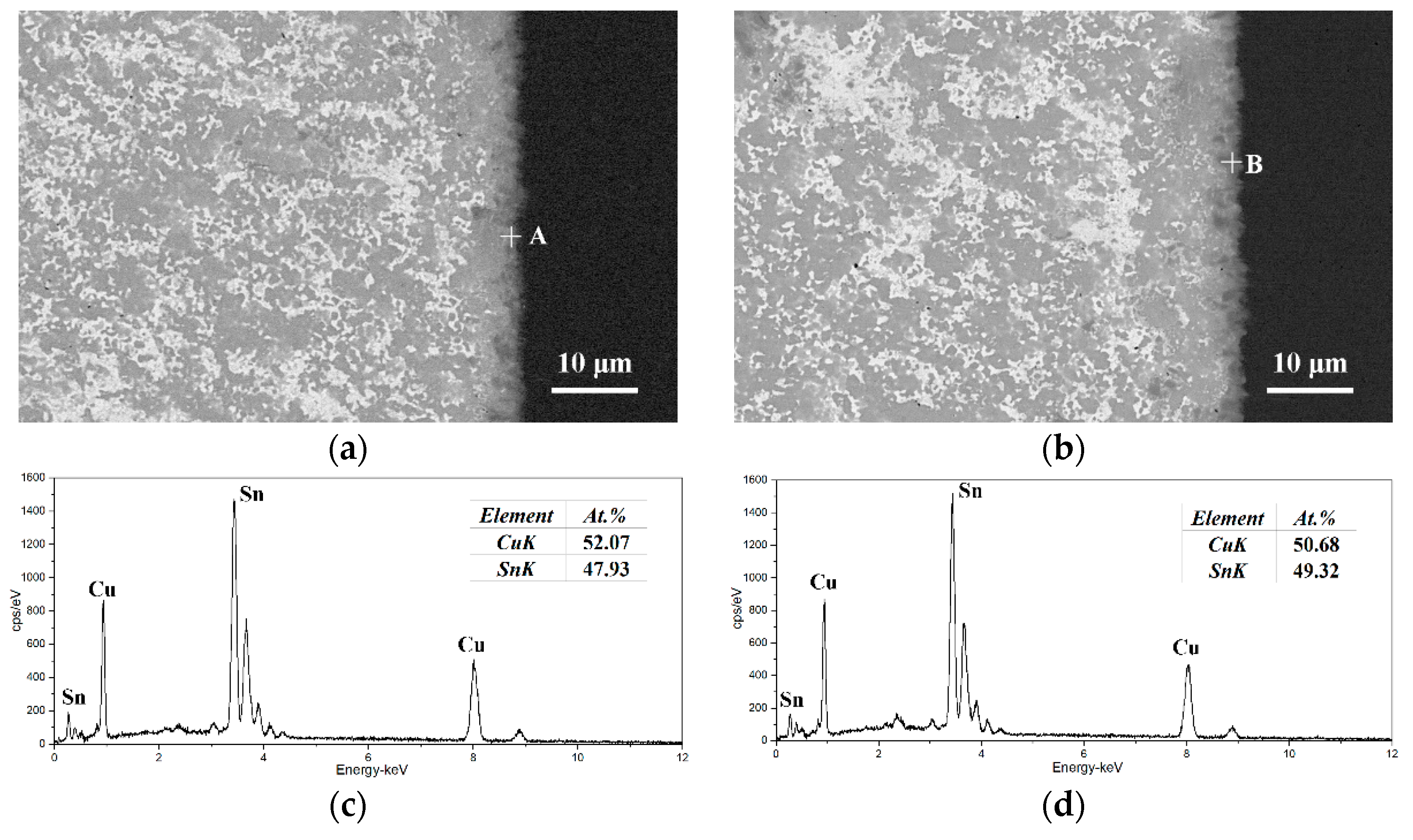
The continuous intermetallic compound (IMC) layer, forming at the interface of the solder and Cu during the soldering process, is fundamental to the efficient metallurgical combination. However, the brittle IMC layer is sensitive to the service conditions and the performance of the solder joint is greatly determined by the thickness and morphology of the IMC layer [13]. Figure 2 shows the interfacial microstructure of the Sn50Pb49Sb1/Cu solder joint at different irradiation doses. According to Figure 2a and the results of the EDS analysis, a continuous Cu6Sn5 layer with a “saw tooth-like” morphology was observed at the interface of the as-soldered joint, which could lead to the conclusion that successful solder joints are prepared due to non-existent defects. As can be seen in Figure 2b, the thickness and morphology of the Sn50Pb49Sb1/Cu solder joint barely changed after being irradiated for 960 h, and the EDS results in Figure 2d show that the composition of the IMC layer was still Cu6Sn5. Therefore, the effect of γ-ray irradiation on the interfacial microstructure of the Sn50Pb49Sb1/Cu solder joint could be considered unapparent.
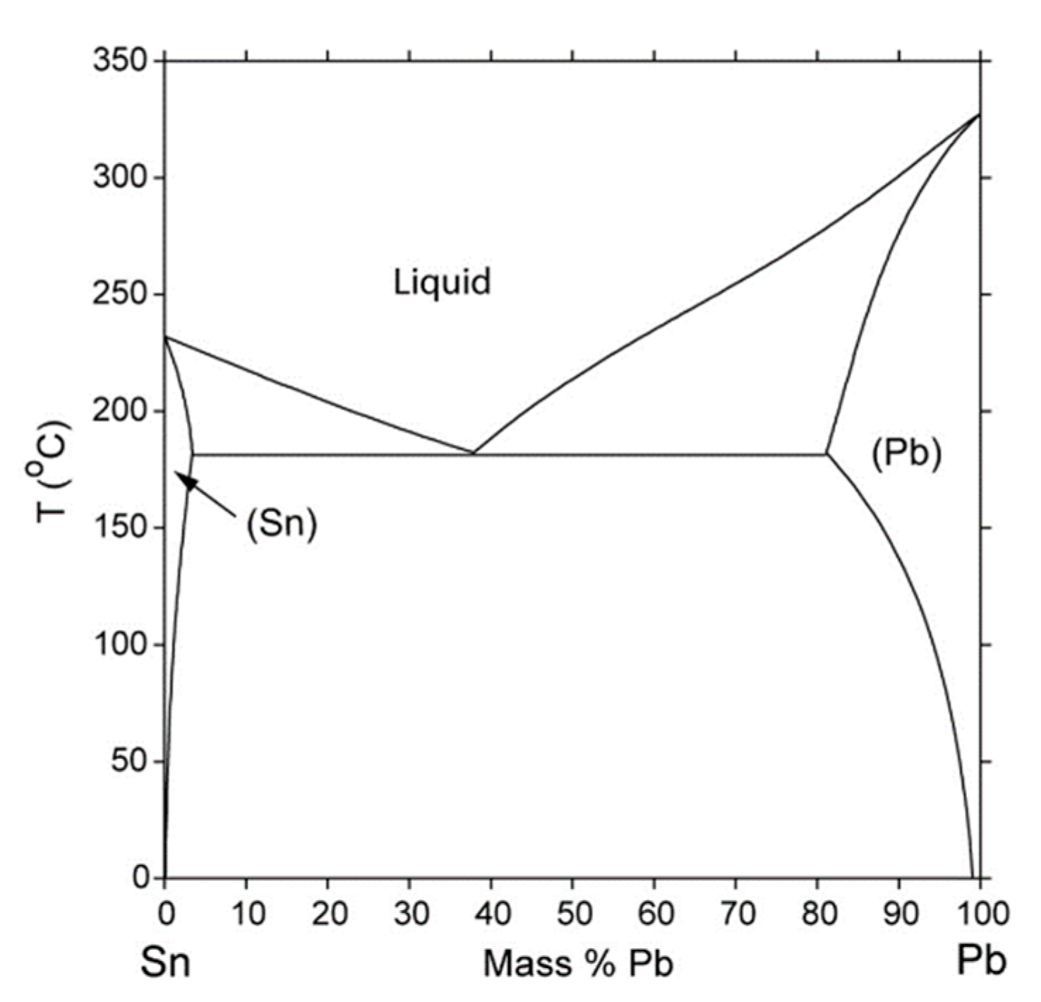
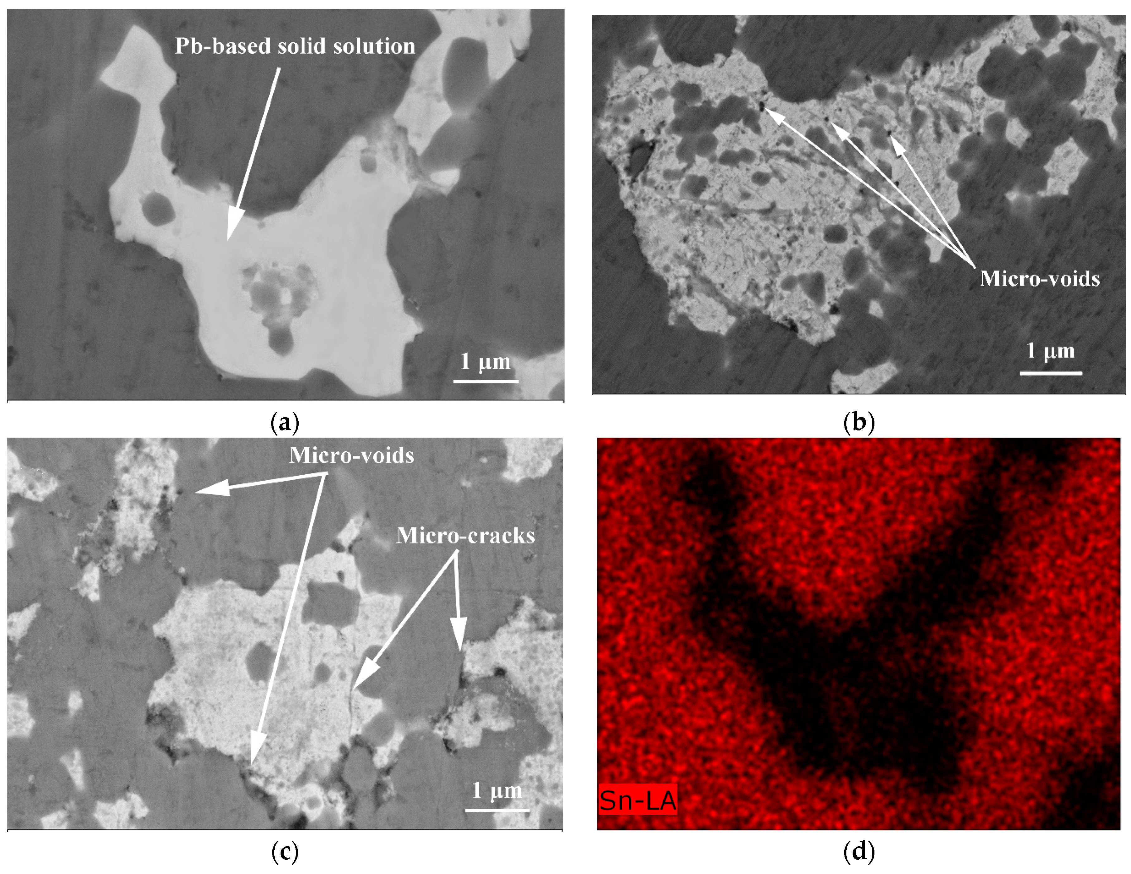
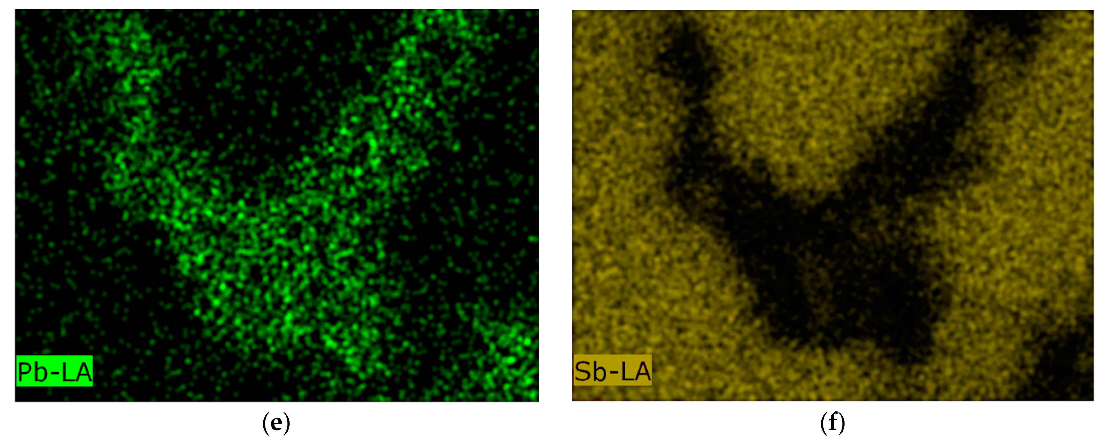
In the SnPb solder, tin and lead dissolved mutually, forming a solid solution. No IMC was generated based on the Sn-Pb binary phase diagram, as shown in Figure 3. Moreover, Sb could not react with neither Sn nor Pb, and only dissolved in the Sn-based solid solution [14]. Figure 4 shows the solder-side microstructure of the Sn50Pb49Sb1/Cu solder joint at various irradiation doses. As can be seen from Figure 4d,e, the element mapping results of Figure 4a show that the microstructure of the solder joint consists of two phases: an Sn-based solid solution that is red in Figure 4d, and a Pb-based solid solution that is green in Figure 4e. Moreover, the trace amount of Sb only dissolved in the Sn-based solid solution. In the as-soldered joint, the Pb-based solid solution with a flat and intact morphology was observed, as shown in Figure 4a. However, micro-voids and micro-cracks were found in some Pb-based solid solutions after γ-ray irradiation. These defects expanded with the increasing irradiation dose.
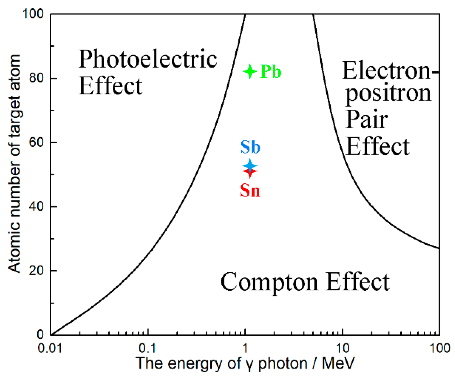
There are two types of γ photons that 60Co emits: 1.17 MeV and 1.33 MeV. Based on this energy level, the Compton effect mainly occurred in the Sn50Pb49Sb1/Cu solder joint subjected to γ-ray irradiation, as shown in Figure 5. Displaced atoms induced directly by the collision of the γ photon and nucleus could be ignored due to their low cross section, but energetic electrons generated by γ-ray irradiation through the Compton effect could bring about many point defects [15]. The energy relationship of the incident γ photon and energetic electron (Ee) is given by:
where Eγ is the energy of the incident γ photon, and mec2 is the rest energy of electron. Figure 6 shows the schematic diagram of micro-defect generation in the Pb-based solid solution during the irradiation process. Based on Equation (1), the energetic electron induced by the γ photon could knock the Pb atom out and form both a displaced atom and a vacant lattice site, which is known as Frenkel disorder, as shown in Figure 6a. During the irradiation process, a part of these defects were annihilated by migration, whereas other parts retained and expanded with the accumulation of irradiation dose, forming micro-voids and micro-cracks, as illustrated in Figure 6b,c. In addition, it is well known that the interaction of the Compton process is proportional to the atomic number (Z) of the target material. Hence, the γ photon is apt to penetrate the Sn-based solid solution rather than collide with the Sn atom due to the lower Z of Sn [16]. Therefore, little evolution of the Sn-based solid solution was observed in comparison with the Pb-based solid solution. Moreover, there was no formation of a Sb-rich phase or segregation of the Sb element after irradiation. However, further research on the effect of γ-ray irradiation on the solute atom is necessary.
3.2. Pull Force
As can be seen from Figure 7, the strength of the Sn50Pb49Sb1/Cu solder joint attenuated with the increasing irradiation dose. After being irradiated for 960 h, the pull force of the solder joint decreased by 22%. Compared with the preliminary stage of irradiation, the graph reveals a downward trend in the reduction rate of the pull force under a heavy dose of irradiation. The formation and expansion of micro-voids and micro-cracks induced by γ-ray irradiation, which are the generation source of cracks, increased the fracture risk of the joint with outer stress, and hence reduced the strength of the solder joint. The increasing accumulation of irradiation dose amassed displaced atoms and lattice vacancies in the Pb-based solid solution and both types of point defects were supersaturated after long-term γ-ray irradiation. This may increase the formation difficulty of new micro-defects due to the rising inner stress and, therefore, lead to a slowdown in strength decrement after a heavy dose of irradiation, as shown in Figure 7. However, further research on the atomic scale is necessary to verify this discussion.
3.3. Fracture Morphology
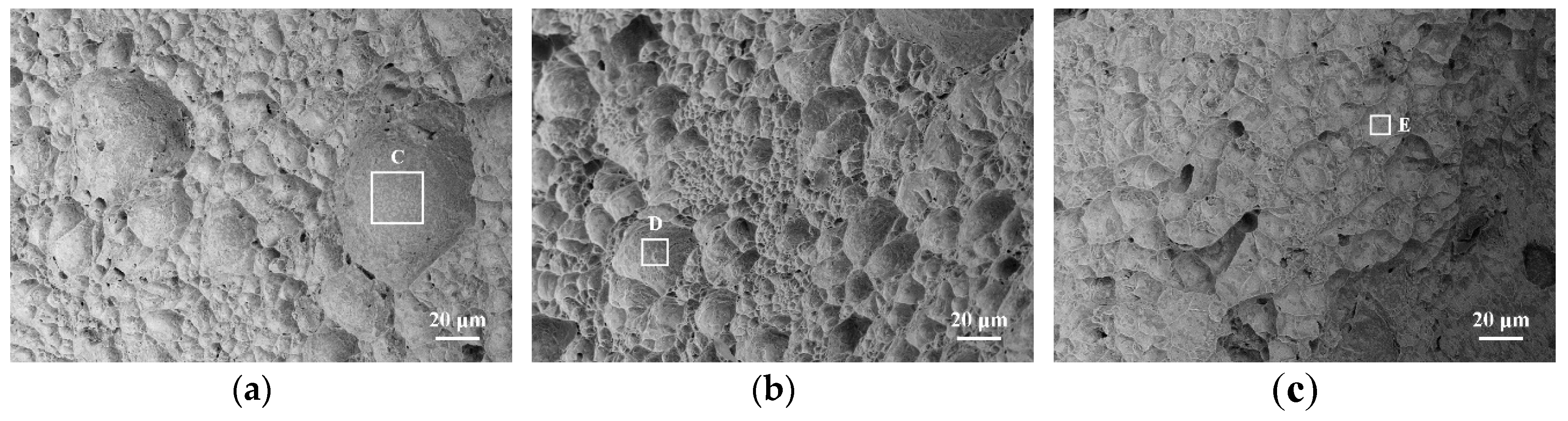
For the sake of understanding the failure behavior and characteristics of Sn50Pb49Sb1/Cu solder joints after γ-ray irradiation, fracture morphology was observed using SEM and EDS. The SEM images of the fracture morphology of joints at various irradiation times was carried out after pull tests, as shown in Figure 8. The SEM fractography of the joints with three different irradiation times exhibited fracture surfaces with typical ductile dimples, which shows evidence of a great quantity of plastic deformation along the loading direction. It also demonstrates that the fracture type of Sn50Pb49Sb1/Cu solder joints is incapable of being changed by γ-ray irradiation, which is still a ductile fracture. Furthermore, as can be seen from Table 1, the chemical composition of dimples in the solder joints before/after irradiation was mainly Sn and Pb. Hence, it could be inferred that the tensile fractures all occurred within the solder bulk, which is very different to other reliability tests. However, as can be seen from Figure 8b,c, the depth and size of the dimples of the Sn50Pb49Sb1/Cu solder joint after 960 h irradiation decreased in comparison with the as-soldered joint, which could be explained by irradiation embrittlement. Numerous displaced atoms and lattice vacancies were generated by γ photons through the Compton effect, and the supersaturation of point defects improved the resistance of the dislocation glide, making solder joints difficult to deform [17,18]. With the accumulation of the irradiation dose, the dimples of the broken joints were slightly less obvious than as-soldered joints, which indicates that the ductility of the Sn50Pb49Sb1/Cu solder joint decreased during the irradiation process.
4. Conclusions
In this study, the microstructure and performance evolution of Sn50Pb49Sb1/Cu solder joints exposed to γ-ray irradiation were investigated. γ-ray irradiation had little effect on the interfacial layer of solder joints, but the formation and expansion of micro-voids and micro-cracks were observed in the Pb-based solid solution during the irradiation process, which reduced the strength of the joint. Compared with the as-soldered joint, the pull force of the Sn50Pb49Sb1/Cu solder joint after 960 h irradiation decreased by 22%. In addition, γ-ray irradiation could not change the fracture type of the Sn50Pb49Sb1/Cu solder joint, however a slight decrement of ductility was observed after irradiation. The results of this paper are conducive to comprehending the reliability and sensitivity of solder joints under the cosmic radiation environment and provide references for the design and manufacture of future small satellites. As the actual service environment of satellites consists of cosmic radiation, extreme temperature variations and vibration, further investigations of the combined effect of the conditions mentioned above on the reliability of solder joints are necessary for the design of excellent solder alloys for use in deep space satellites.
Author Contributions
S.X. and J.W. conceived and designed the experiments; J.W., L.W. and S.L. performed the experiments; J.W. and Z.L. analyzed the data; S.X. contributed materials and analysis tools. J.W. wrote the paper.
Funding
This research was funded by the National Natural Science Foundation of China, grant No. 51675269 and the Priority Academic Program Development of Jiangsu Higher Education Institutions (PAPD).
Conflicts of Interest
The authors declare no conflict of interest.
References
- Liao, M.-C.; Huang, P.-S.; Lin, Y.-H.; Tsai, M.-Y.; Huang, C.-Y.; Huang, T.-C. Measurements of Thermally-Induced Curvatures and Warpages of Printed Circuit Board during a Solder Reflow Process Using Strain Gauges. Appl. Sci. 2017, 7, 739. [Google Scholar] [CrossRef]
- Zeng, K.; Tu, K.N. Six cases of reliability study of Pb-free solder joints in electronic packaging technology. Mater. Sci. Eng. R 2002, 38, 55–105. [Google Scholar] [CrossRef]
- Chen, C.; Tong, H.M.; Tu, K.N. Electromigration and Thermomigration in Pb-Free Flip-Chip Solder Joints. Annu. Rev. Mater. Res. 2010, 40, 531–555. [Google Scholar] [CrossRef]
- Adriani, O.; Barbarino, G.C.; Bazilevskaya, G.A.; Bellotti, R.; Boezio, M.; Bogomolov, E.A.; Bongi, M.; Bonvicini, V.; Borisov, S.; Bottai, S.; et al. Cosmic-Ray Electron Flux Measured by the PAMELA Experiment between 1 and 625 GeV. Phys. Rev. Lett. 2011, 106, 201101. [Google Scholar] [CrossRef] [PubMed] [Green Version]
- Badhwar, G.D.; O’Neill, P.M. Galactic cosmic radiation model and its applications. Adv. Space Res. 1996, 17, 7–17. [Google Scholar] [CrossRef]
- Zhong, W.H.; Sui, G.; Jana, S.; Miller, J. Cosmic radiation shielding tests for UHMWPE fiber/nano-epoxy composites. Compos. Sci. Technol. 2009, 69, 2093–2097. [Google Scholar] [CrossRef]
- Baker, D.N.; Worden, S.P. The Large Benefits of Small-Satellite Missions. Eos Trans. Am. Geophys. Union 2013, 89, 301–302. [Google Scholar] [CrossRef]
- Nishida, S.-I.; Kawamoto, S.; Okawa, Y.; Terui, F.; Kitamura, S. Space debris removal system using a small satellite. Acta Astronaut. 2009, 65, 95–102. [Google Scholar] [CrossRef]
- Arnieri, E.; Boccia, L.; Amendola, G.; Massa, G.D. A Compact High Gain Antenna for Small Satellite Applications. IEEE Trans. Antennas Propag. 2007, 55, 277–282. [Google Scholar] [CrossRef]
- Tu, K.N.; Zeng, K. Tin–lead (SnPb) solder reaction in flip chip technology. Mater. Sci. Eng. R 2001, 34, 1–58. [Google Scholar] [CrossRef]
- Aktas, O.; Kuliev, A.; Kumar, V.; Schwindt, R.; Toshkov, S.; Costescu, D.; Stubbins, J.; Adesida, I. 60Co gamma radiation effects on DC, RF, and pulsed I–V characteristics of AlGaN/GaN HEMTs. Solid State Electron. 2004, 48, 471–475. [Google Scholar] [CrossRef]
- Karataş, Ş.; Türüt, A.; Altındal, Ş. Effects of 60Co γ-ray irradiation on the electrical characteristics of Au/n-GaAs (MS) structures. Nucl. Instrum. Meth. A 2005, 555, 260–265. [Google Scholar] [CrossRef]
- Che, F.X.; Pang, J.H.L. Characterization of IMC layer and its effect on thermomechanical fatigue life of Sn–3.8Ag–0.7Cu solder joints. J. Alloys Compd. 2012, 541, 6–13. [Google Scholar] [CrossRef]
- El-Daly, A.A.; Hammad, A.E.; Fawzy, A.; Nasrallh, D.A. Microstructure, mechanical properties, and deformation behavior of Sn–1.0Ag–0.5Cu solder after Ni and Sb additions. Mater. Des. 2013, 43, 40–49. [Google Scholar] [CrossRef]
- Wang, L.; Tang, J.; Huang, Q.-A. Gamma and electron beam irradiation effects on the resistance of micromachined polycrystalline silicon beams. Sens. Actuators A Phys. 2012, 177, 99–104. [Google Scholar] [CrossRef]
- Murty, R.C. Effective Atomic Numbers of Heterogeneous Materials. Nature 1965, 207, 398–399. [Google Scholar] [CrossRef]
- Wakai, E.; Jitsukawa, S.; Tomita, H.; Furuya, K.; Sato, M.; Oka, K.; Tanaka, T.; Takada, F.; Yamamoto, T.; Kato, Y.; et al. Radiation hardening and embrittlement due to He production in F82H steel irradiated at 250°C in JMTR. J. Nucl. Mater. 2005, 343, 285–296. [Google Scholar] [CrossRef]
- Lambrecht, M.; Malerba, L.; Almazouzi, A. Influence of different chemical elements on irradiation-induced hardening embrittlement of RPV steels. J. Nucl. Mater. 2008, 378, 282–290. [Google Scholar] [CrossRef]
Figure 1.
Diagram of 45° pull test of solder joints on QFP lead.

Figure 2.
The interfacial microstructure of the Sn50Pb49Sb1/Cu solder joint at different irradiation times: (a) 0 h; (b) 960 h; (c) EDS results of point A; (d) EDS results of point B.
Figure 2.
The interfacial microstructure of the Sn50Pb49Sb1/Cu solder joint at different irradiation times: (a) 0 h; (b) 960 h; (c) EDS results of point A; (d) EDS results of point B.

Figure 3.
Binary phase diagram of tin and lead.

Figure 4.
SEM and element mapping of the Sn50Pb49Sb1/Cu solder joint after being irradiated for: (a) 0 h; (b) 480 h (c) 960 h, and element mapping of: (d) Sn; (e) Pb; (f) Sb.
Figure 4.
SEM and element mapping of the Sn50Pb49Sb1/Cu solder joint after being irradiated for: (a) 0 h; (b) 480 h (c) 960 h, and element mapping of: (d) Sn; (e) Pb; (f) Sb.


Figure 5.
Domination region of three effects of γ-rays on target materials.

Figure 6.
Schematic diagram of micro-defect generation in the Pb-based solid solution: (a) the formation of point defects induced by γ-ray; (b) the migration of lattice vacancy; (c) the formation of micro-defects.
Figure 6.
Schematic diagram of micro-defect generation in the Pb-based solid solution: (a) the formation of point defects induced by γ-ray; (b) the migration of lattice vacancy; (c) the formation of micro-defects.

Figure 7.
The pull force of the Sn50Pb49Sb1/Cu solder joint at various irradiation times.

Figure 8.
Fracture morphology of the solder joint after pull tests at various irradiation times: (a) 0 h; (b) 480 h; (c) 960 h.
Figure 8.
Fracture morphology of the solder joint after pull tests at various irradiation times: (a) 0 h; (b) 480 h; (c) 960 h.


Table 1.
EDS analysis of region C, D and E (at. %).
| Region | Sn | Pb | Sb | Cu |
|---|---|---|---|---|
| C | 64.49 | 33.91 | 0.96 | 0.64 |
| D | 59.88 | 38.56 | 1.08 | 0.48 |
| E | 61.6 | 36.82 | 0.87 | 0.71 |
© 2018 by the authors. Licensee MDPI, Basel, Switzerland. This article is an open access article distributed under the terms and conditions of the Creative Commons Attribution (CC BY) license (http://creativecommons.org/licenses/by/4.0/).
Share and Cite
MDPI and ACS Style
Wang, J.; Xue, S.; Lv, Z.; Wen, L.; Liu, S. Study on the Reliability of Sn50Pb49Sb1/Cu Solder Joints Subjected to γ-ray Irradiation. Appl. Sci. 2018, 8, 1706. https://doi.org/10.3390/app8101706
AMA Style
Wang J, Xue S, Lv Z, Wen L, Liu S. Study on the Reliability of Sn50Pb49Sb1/Cu Solder Joints Subjected to γ-ray Irradiation. Applied Sciences. 2018; 8(10):1706. https://doi.org/10.3390/app8101706
Chicago/Turabian StyleWang, Jianhao, Songbai Xue, Zhaoping Lv, Li Wen, and Siyi Liu. 2018. "Study on the Reliability of Sn50Pb49Sb1/Cu Solder Joints Subjected to γ-ray Irradiation" Applied Sciences 8, no. 10: 1706. https://doi.org/10.3390/app8101706
Note that from the first issue of 2016, this journal uses article numbers instead of page numbers. See further details here.