Article

Enhanced Thermochromic Properties of Vanadium Dioxide (VO2)/Glass Heterostructure by Inserting a Zr-Based Thin Film Metallic Glasses (Cu50Zr50) Buffer Layer

1
School of Physics and Electronic Information, Henan Polytechnic University, Jiaozuo 454000, China
2
School of Electronic Science and Applied Physics, Lab of Quantum Materials and Interfaces, Hefei University of Technology, Hefei 230009, China
*
Author to whom correspondence should be addressed.
Appl. Sci. 2018, 8(10), 1751; https://doi.org/10.3390/app8101751
Submission received: 15 August 2018 / Revised: 14 September 2018 / Accepted: 21 September 2018 / Published: 28 September 2018
(This article belongs to the Special Issue Metal-Insulator Transitions)

Abstract

:

Featured Application

Smart windows and other transferable infrared devices.

Abstract

Vanadium dioxide (VO2) with reversible metal–insulator transition (MIT) is one of the most promising energy-efficient materials. Especially for VO2-based smart windows, the visible transmittance and solar modulation ability are the most critical parameters. However, VO2 thin films that are directly deposited onto glass substrates are of poor crystallinity and MIT performance, limiting the practical applications of VO2/glass heterostructures. In this paper, a buffer layer of Cu50Zr50 was introduced to build a novel Zr-based thin film metallic glass (VO2/Cu50Zr50/glass) with multilayer structures for thermochromic applications. It is observed that the insertion of a Cu50Zr50 buffer layer with appropriate thickness results in a clear enhancement of crystalline quality and MIT performance in the VO2/Cu50Zr50/glass thin films, compared with the single-layer VO2/glass thin films. Moreover, the VO2/Cu50Zr50/glass bi-layer films exhibit better optical performance with enhanced solar modulation ability (ΔTsol = 14.3%) and a high visible transmittance (Tvis = 52.3%), which represents a good balance between ΔTsol and Tvis for smart window applications.

Graphical Abstract

1. Introduction

In response to a large energy-consuming and environmentally deteriorating condition, developing energy-saving materials and sustainable energy has aroused wide attention. Vanadium dioxide (VO2) thin film is a first-order phase-changed material with superfast reaction speed that is near the critical temperature, 340 K [1,2]. This phase transformation is called a metal–insulator transition (MIT), and involves significant changes in electrical and optical characteristics. Its phase switching behavior makes VO2 a hopeful candidate for a variety of applications, such as smart windows [3], sensor devices [4], ultrafast switches [5], Mott field effect transistors [4,6], etc.
Various techniques have been developed to form VO2 thin films, for instance, molecular beam epitaxy [7], pulsed laser deposition [8], magnetron sputtering [9], and chemical vapor deposition [10]. Over the past decades, high-quality VO2 thin films with the single crystalline characteristics have been seeking because of the impact on MIT features. It is known that the characteristics of the chosen substrates play a major role in the thermochromic properties of VO2 thin films [11,12]. A lot of single crystals have been employed to act as the growth substrates, such as titanium dioxide (TiO2), silica (SiO2), sapphire (Al2O3), and magnesium fluoride (MgF2). The employ of single crystals results in a high expense for the device preparations and therefore immensely limits practical manufacture based on VO2 thin films. As an alternative approach, common glass substrates with very low cost and good optical transmittance are potentially promising for the production of smart windows and other transferable infrared devices. However, VO2 thin films that are directly grown onto conventional glass substrates are generally of poor crystallinity. Hence, single-layer VO2/glass thin films have worse MIT and photoelectric properties [13,14]. In particular, the luminous transmittance and solar modulation ability are often especially bad in single-layer VO2/glass structures, which limits the practical manufacture of VO2-based smart windows. Thus, it is the need of the immediate to find a way to optimize the crystallinity and photoelectric properties in VO2/glass heterostructures.
One way to do this is to design and fabricate a multilayered structure. Multilayered VO2 thin films have been completed on different substrates by use of “buffer layers” of materials, such as TiO2, SnO2, ZnO [15,16,17], conductive oxides (Aluminum-doped Zinc Oxied (AZO), Fluorine Tin Oxide (FTO), Indium Tin Oxide (ITO), etc.) [18,19,20], metals (Ag, Cu, etc.), thin films [21], etc. Recently, thin film metallic glasses (TFMGs) were introduced and showed better surface roughness [22] and good optical properties [23,24]. In particular, Zr-based TFMG have received much scientific research attention for potential applications, since their good mechanical, tribological and fatigue properties, and their corrosion resistance and excellent adhesion [25,26,27,28]. Recently, Zong found that the Zr-based thin film metallic glasses (Cu50Zr50) have excellent near-infrared transmission (larger than 80%) [28]. Cu50Zr50, which can be prepared at room temperature, is a good candidate for template layers. The excellent near-infrared transmission and the appearance of the surface plasmon polaritons (SPPs) is anticipated to be favorable for the optical property of VO2 thin films.
Motivated by the above demands for the thermochromic application of VO2/glass thin films, in the present study we constructed a Zr-based thin film metallic glass (VO2/Cu50Zr50/glass) with a multilayer structure, consisting of Cu50Zr50 TFMG as a buffer layer on amorphous glass substrates. The thickness dependence of the microstructure and optoelectronic properties of the VO2/Cu50Zr50/glass multilayers was investigated. The achievements may be more comprehensive to understand the role of Cu50Zr50 buffer layers in the formation of high-crystalline VO2 thin films on glass substrates, and thus pave a way towards heightening the photoelectrical properties of VO2 thin film-based devices.

2. Experimental

2.1. Method for Film Deposition

VO2/glass monolayer and VO2/Cu50Zr50/glass bilayer structures (different Cu50Zr50 buffer layer thicknesses) were prepared by pulsed laser deposition (wavelength 248 nm). The targets are V (99.95% purity, 25 mm diameter, 3 mm thick) and Cu50Zr50 alloy (99.99% purity, 40 mm diameter, 5 mm thick). Cleaned the amorphous glass substrates (BF33) with an ethanol/acetone solution, rinsed with distilled water, and finally blown with pure nitrogen. Prior to deposition, the base pressure was controlled at 1.0 × 10⁻⁴ Pa and the target-substrate distance was 6 cm. During the deposition, the laser operated at repetition rate of 5 Hz and output pulse energy of 200 mJ for entire deposition, the target and substrate were rotated at a rate of 18 rpm. The deposition conditions for the VO2 film and buffer layer were 500 °C with PO2 = 0.9 Pa for VO2 film, room temperature without oxygen inlet for Cu50Zr50. The oxygen flow rate was 25 sccm for VO2. The film thickness was controlled by deposition time and corrected by step profiler (DektakXT, Bruker, Karlsruhe, Germany). The Cu50Zr50 buffer layers had thicknesses of 40 nm, 80 nm, and 160 nm in the three multilayer VO2/Cu50Zr50/glass thin films. For comparison, the single-layer VO2 thin films were grown directly on an amorphous glass substrate under the same conditions as the VO2/Cu50Zr50/glass thin films. The thickness of all the VO2 thin films was 60 nm. The four thin films were marked as VO2(60 nm)/glass, VO2(60 nm)/Cu50Zr50(40 nm)/glass, VO2(60 nm)/Cu50Zr50(80 nm)/glass, and VO2(60 nm)/Cu50Zr50(160 nm)/glass.

2.2. Film Characterization

The crystallographic properties of the sample was characterized by X-ray diffraction (XRD) using a instrument modeled LabXRD-6000 (Shimadzu, Kyushu, Japan) (λ = 0.15406 nm). Using atomic force microscopy (AFM), the surface morphology of the samples was studied with a profilometer (Dektak 150, Bruker, Karlsruhe, Germany)). Images were additionally acquired by scanning electron microscopy (SEM) (Zeiss Supa 50VP, Jena Germany). The temperature-driven MIT properties were measured during the heating and cooling process within the temperature range 30–120 °C by the Hall Effect Measurement System (HMS-5300, Ecopia, Pyeongchang, South Korea). A double beam spectrophotometer (UV-3600, Shimadzu, Kyushu, Japan) with a spectral range of 200–2650 nm was used to record the transmittance spectra of the films. The temperature was controlled in situ by a heater.

3. Results and Discussion

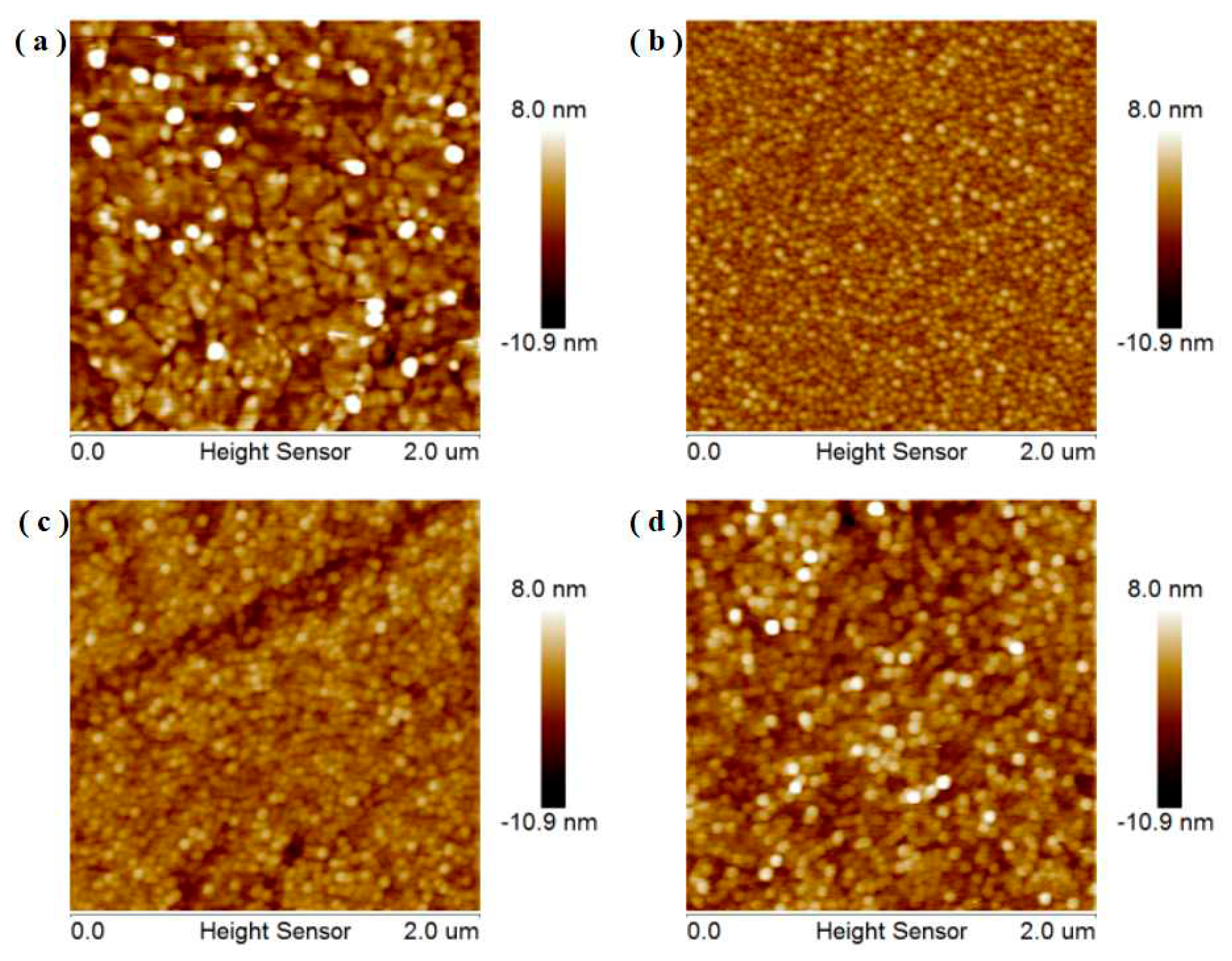
3.1. Microstructural Properties

Figure 1 shows the XRD diffraction patterns of the VO2/glass film and VO2/Cu50Zr50/glass films. The generalized diffraction with the 2θ ranging from 15° to 30° indicates the glass properties of the substrates. For the thin films, the peaks that were located at 27.80° are attributed to the VO2 (011) peak (JCPDS No. 43-1051), which is the feature diffraction peak for M1-phase VO2 thin films [29]. All of the VO2 thin films are strongly oriented along the [011] direction, whether or not buffer layers were inserted on the glass substrate. The diffraction peak located at 31.47° belongs to the ZrO2 (111) peak (JCPDS No. 65-1024), implying the monoclinic symmetry characteristics of the ZrO2. The peak located at 42.42° is assigned to the Cu2O (200) peak (JCPDS No. 77-0199). The appearance of ZrO2 and Cu2O may be due to the incorporation of Zr and Cu ions with oxygen during the VO2 thin film growth. In addition, as the thickness of the buffer layer increases, the intensity of VO2 (011) peaks (in units of counts per second (cps)) initially increases and then decreases, indicating that the crystal quality of VO2 thin films initially improves and then worsens. The characteristic peaks of the VO2 phase disappear in the 160 nm-thick VO2/Cu50Zr50/glass thin films, which clearly indicates that thicker buffer layers make VO2 amorphous.
Figure 2 shows the AFM micrographs of the surfaces of the VO2/glass film and VO2/Cu50Zr50/glass films. The surfaces of the VO2/Cu50Zr50/glass films are smoother and more uniform than the VO2/glass film. The measured roughnesses of the VO2/Cu50Zr50/glass films without a buffer layer, and with buffer layers with thicknesses of 40 nm, 80 nm, and 160 nm, are 2.86 nm, 1.32 nm, 1.51 nm, and 2.12 nm, respectively, indicating that the surface morphology of VO2 films that are grown on glass substrates can be optimized effectively by embedding a Cu50Zr50 buffer layer. What calls for special attention is a suitable thickness needs that the Cu50Zr50 buffer layer need to select, since excess thickness of Cu50Zr50 layers will generate rougher films.
To further show the effects of the buffer layer thickness on the microstructures, the SEM images of the surface morphology of the VO2/Cu50Zr50/glass thin films with different buffer layer thicknesses are shown in Figure 3. The surfaces of all the films are found to be continuous and dense. The bright white segments that are visible on the surface of films are identified as amorphous metal V particles, according to the elemental analysis illustrated in the small red circles of Figure 3c,d by Energy-dispersive X-ray spectroscopy (EDS). After embedding an alloy buffer layer, the number of the amorphous metal V particles increases clearly, resulting in poor crystallinity of the VO2 thin films on the thick buffer layer.
By combining the above analysis, the following can be conjectured. When the buffer layer thickness is relatively thin (~40 nm), the incorporation of Zr atoms with O atoms during deposition forms monoclinic ZrO2. The ZrO2 interfacial layer serves as a template to improve the crystallinity of the upper VO2 thin films. This result is highly consistent with the case of the VO2/Y-doped ZrO2/Si thin films [30], where the Y-doped ZrO2 served as the buffer layer. As the buffer layer thickness increases to 80 nm, the high roughness and impure phase of Cu2O deteriorates the crystal quality of the VO2 thin films. When the buffer layer thickness increases to 160 nm, much more oxygen is consumed and too many amorphous metal V particles are present on the film surface, which reduces the crystalline quality of the VO2(M) thin film.

3.2. Electrical Properties

Figure 4 shows the square resistance variation with temperature in the heating and cooling cycles of the VO2 thin films with various thicknesses of Cu50Zr50 inserting buffer layers. In Figure 4a, the VO2/glass thin films show a resistance–temperature curve with a wide transformation hysteresis. In the cases of the 40- and 80-nm-thick buffer layers, the VO2 thin films both exhibit sharper decreases in sheet resistance with increasing temperature, as illustrated in Figure 4b,c, strongly implying the occurrence of an MIT. However, no MIT occurs when the buffer layer thickness attains to 160 nm. This result can be attributed to poor crystallization in the VO2/Cu50Zr50/glass thin films, which is good corresponding to the XRD analysis.
To better comparing, the observed electrical properties of VO2 films with various buffer layer thicknesses are summarized in Table 1. The transition temperature (Tc) is defined as the center of the derivative curve of the heating curve in the insets of Figure 3. Here, we defined the amplitude of MIT (ΔR) as the relative resistance change ratio between room temperature and a temperature of 100 °C. The hysteresis width (ΔH) is the difference between the Tc values that were measured during the heating and cooling cycles. From Table 1, the single-layer VO2 thin films have higher Tc than the buffered VO2 thin films. After introducing the buffer layer (40 nm and 80 nm in thickness), the Tc values of VO2 thin films are similar to that of the bulk VO2 single crystal (68 °C), which is generally due to the release of stress [31]. The ΔR values of the VO2/glass thin films are slightly larger than those of the 40- and 80-nm-thick VO2/Cu50Zr50/glass thin films. This could be due to the larger crystal size in the non-buffered VO2 thin films [32]. The samples with smaller or larger ΔH values can be applied in different fields and the ΔH value is closely connected with the quality of crystallization and crystallite dimension in the VO2 thin films [33,34,35]. From Table 1, it can be seen that the ΔH values of the buffered VO2 thin films are much smaller than the non-buffered one. The buffer layer serves as a good template for VO2 thin film growth and it thus results in a better crystallinity in the 40- and 80-nm-thick VO2/Cu50Zr50/glass thin films. These conclusions point out that the electrical characteristic of VO2 films can be significantly enhanced by inserting Cu50Zr50 buffer layer of appropriate thickness.

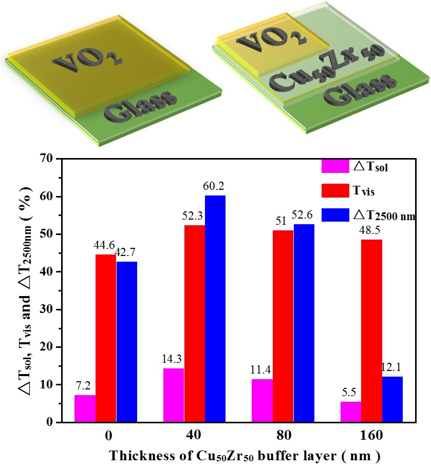
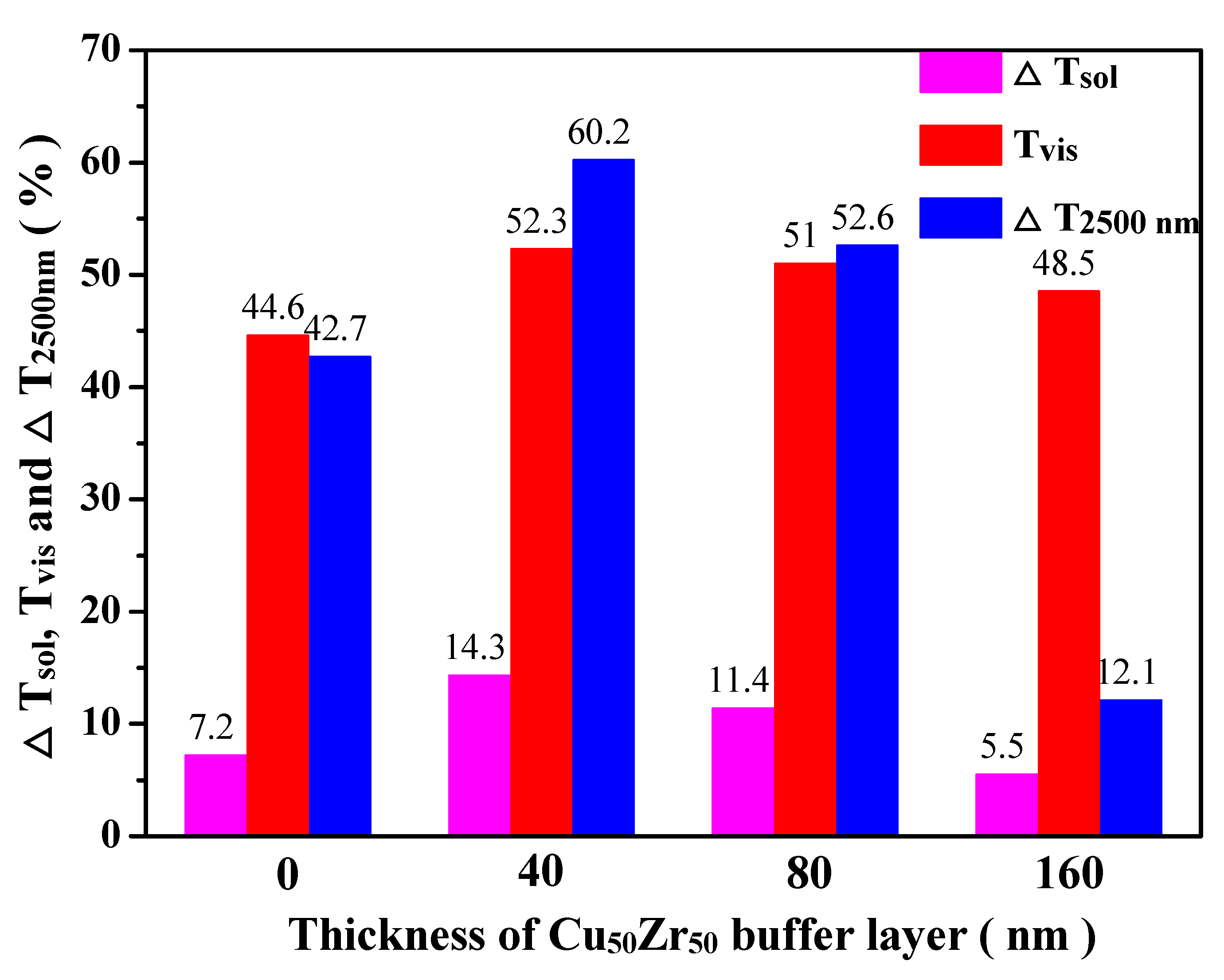
3.3. Optical Properties

The optical parameters of VO2/glass and VO2/Cu50Zr50/glass thin films is measured with in situ varying temperature. Figure 5 depicts the thermochromic transmittance curves of VO2/glass and VO2/Cu50Zr50/glass films in response to preset temperatures (from room temperature to 100 °C). Objectively speaking, the transmittance of all the samples in the visible region is almost constant. However, the transmittance of VO2(60 nm)/glass, VO2(60 nm)/Cu50Zr50(40 nm)/glass, and VO2(60 nm)/Cu50Zr50(80 nm)/glass decreases clearly with the temperature increases in the infrared region, as shown in Figure 5a–c, while in the VO2(60 nm)/Cu50Zr50(160 nm)/glass thin films the transmittance changes relatively little (Figure 5d).
The optical modulation properties of the VO2 thin film are investigated to evaluate its potential in smart windows. In order to realize the applications of VO2 in smart windows, technological challenges need to be addressed, including improving the maximum visible transmittance (Tvis), maintaining high solar modulating efficiency (ΔTsol), and undergoing more than 10,000 cycles without any degradation [36]. The Tvis, ΔTsol, and near-infrared (NIR) switching efficiency (ΔT2500nm) of all the samples were obtained by the calculation of the transmittance spectra and are displayed in Figure 6. The solar transmittance (Tsol, 300–2500 nm) and the ΔTsol values are derived from the following formulas:
T s o l = φ s o l ( λ ) T ( λ ) d λ φ s o l ( λ ) d λ  
Δ T s o l = T s o l ( 30   C ) T s o l ( 100   C )  
where T(λ) is defined as the transmittance at wavelength λ and φsol is the solar irradiance spectrum for air mass 1.5 (corresponding to the sun standing 37° above the horizon) [37]. As shown in Figure 6, the Tvis, ΔTsol, and ΔT2500nm values of the monolayer VO2 film are 44.6%, 7.2% and 42.7%, respectively. Therefore, the good thermochromic properties with enhanced luminous transmittance is obtained by introducing Cu50Zr50 as buffer layer, possibly because Cu50Zr50 can act as an anti-reflection layer (AR) for VO2 films. When compared with the VO2(60 nm)/glass, the samples of VO2(60 nm)/Cu50Zr50(40 nm)/glass and VO2(60 nm)/Cu50Zr50(80 nm)/glass have higher ΔTsol and Δ T2500nm values. According to [28], Cu50Zr50 possesses a metallic property in the infrared region. For the sandwich structure VO2/Cu50Zr50/glass, p-polarized SPPs are supported on the metallic film interfaces in the corresponding range. The appearance of the SPPs probably effectively modulates the optical properties. This mechanism will be further studied in the future [38,39]. When increasing the Cu50Zr50 buffer layer thickness to 160 nm, the ΔTsol and ΔT2500nm values clearly decreased. The main reason for this is the effect of crystallization quality, which corresponds to the above XRD data analysis. Favorable thermochromic properties are achieved in the sample of VO2(60 nm)/Cu50Zr50(40 nm)/glass. The sample of VO2(60 nm)/Cu50Zr50(40 nm)/glass shows better optical thermochromic performance, and the ΔTsol value is as high as ~14.3% with the Tvis value up to 52.3% and the ΔT2500nm value up to 60.2%, which represents a good balance between ΔTsol and Tvis for smart window applications. These results can be compared with previous experimental results, such as those for periodic and aperiodic porous VO2(M1) films that were prepared through complex chemical and physical processes in multiple layers of TiO2(or SiO2)/VO2/substrate films [40,41,42] and VO2-based composite thin films [43,44]. All in all, optimizing optical properties of VO2 films had indeed been enhanced by the introduction of Cu50Zr50 buffer layer.

4. Conclusions

To conclude, VO2 thin films with monoclinic crystal phase are here successfully grown on glass substrates by PLD (Plused Laser Deposition) techniques. Cu50Zr50 buffer layers of various thicknesses were introduced to modulate the MIT and optical properties. It is observed that a pronounced smaller ΔH across the MIT is achieved in the optimized VO2 (60 nm)/Cu50Zr50(40 nm)/glass film. The ΔTsol value is as high as ~14.3%, with the Tvis value up to 52.3%. A ΔT2500nm value of up to 60.2% is achieved in the VO2 (60 nm)/Cu50Zr50(40 nm)/glass film. The present study suggests that the introduction of a Cu50Zr50 buffer layer of appropriate thickness on a glass substrate is beneficial to the improvement of crystalline quality and thermochronic properties of VO2 thin films, which makes VO2 a candidate material for use in photoelectronic devices and smart windows.

Author Contributions

C.K. and Y.Y. conceived this paper based on previous work. C.Z., Y.Y. and H.Z. contributed to the experimental work. C.K. wrote the paper with input from all authors. Y.Y, L.Z. and M.L. discussed this work and commented on this manuscript.

Funding

This research was funded by by the National Natural Science Foundation of China (No.11405045, 51402281, 11775224 and 11304081), the Program for Innovative Research Team of Henan Polytechnic University, China (No. T2017-2) and the Fundamental Research Funds for the Central Universities of Hefei University of Technology, China (No. 108-4115100092).

Conflicts of Interest

The authors declare no conflict of interest.

References

  1. Morin, F.J. Oxides which show a metal-to-insulator transition at the neel temperature. Phys. Rev. Lett. 1959, 3, 34–36. [Google Scholar] [CrossRef]
  2. Chen, W.; Zhang, Y.Z.; Zhang, C.J.; Zhu, L.G.; Wang, S.M.; Wang, B.X. Thermomechanical analysis and optimisation for beam blank continuous casting. Ironmak. Steelmak. 2013, 35, 129–136. [Google Scholar] [CrossRef]
  3. Wang, S.; Liu, M.; Kong, L.; Long, Y.; Jiang, X.; Yu, A. Recent progress in VO2, smart coatings: strategies to improve the thermochromic properties. Prog. Mater. Sci. 2016, 81, 1–54. [Google Scholar] [CrossRef]
  4. Kim, H.T.; Chae, B.G.; Youn, D.H.; Maeng, S.L.; Kim, G.; Kang, K.Y.; Lim, Y.S. Mechanism and observation of mott transition in VO2-based two-and three-terminal devices. New J. Phys. 2004, 6, 52. [Google Scholar] [CrossRef]
  5. Cavalleri, A.; Tóth, C.; Siders, C.W.; Squier, J.A.; Ráksi, F.; Forget, P.; Kieffer, J.C. Femtosecond structural dynamics in VO2 during an ultrafast solid-solid phase transition. Phys. Rev. Lett. 2001, 87, 237401. [Google Scholar] [CrossRef] [PubMed]
  6. Zhou, C.; Newns, D.M.; Misewich, J.A.; Pattnaik, P.C. A field effect transistor based on the Mott transition in a molecular layer. Appl. Phys. Lett. 1997, 70, 598–600. [Google Scholar] [CrossRef] [Green Version]
  7. Bian, J.M.; Wang, M.H.; Sun, H.J.; Liu, H.Z.; Li, X.X.; Luo, Y.M.; Zhang, Y.Z. Thickness-Modulated Metal–Insulator Transition of VO2 Film Grown On Sapphire Substrate by MBE. J. Mater. Sci. 2016, 51, 6149–6155. [Google Scholar] [CrossRef]
  8. Jian, J.; Wang, X.J.; Li, L.G.; Fan, M.; Zhang, W.; Huang, J.J.; Qi, Z.M.; Wang, H.Y. Continuous Tuning of Phase Transition Temperature in VO2 Thin Films On c-Cut Sapphire Substrates Via Strain Variation. ACS Appl. Mater. Inter. 2017, 9, 5319–5327. [Google Scholar] [CrossRef] [PubMed]
  9. Yang, Y.J.; Wang, L.X.; Huang, H.L.; Kang, C.Y.; Zong, H.T.; Zou, C.W.; Lu, Y.L.; Li, X.G.; Hong, B.; Gao, C. Controlling Metal-Insulator Transition in (010)-VO2/(0001)-Al2O3 Epitaxial Thin Film through Surface Morphological Engineering. Ceram. Int. 2018, 44, 3348–3355. [Google Scholar] [CrossRef]
  10. Zhou, H.J.; Li, J.H.; Xin, Y.C.; Cao, X.; Bao, S.H.; Jin, P. Electron Transfer Induced Thermochromism in a VO2-graphene-Ge Heterostructure. J. Mater. Chem. C 2015, 3, 589–597. [Google Scholar] [CrossRef]
  11. Babkin, E.V.; Charyev, A.A.; Dolgarev, A.P.; Urinov, H.O. Metal-insulator phase transition in VO2: influence of film thickness and substrate. Thin Solid Films 1987, 150, 11–14. [Google Scholar] [CrossRef]
  12. György, J.K.; Danilo, B.; Ilona, S.; Helfried, R.; René, H.; Heidemarie, S. Effect of the substrate on the insulator–metal transition of vanadium dioxide films. J. Appl. Phys. 2011, 109, 582. [Google Scholar]
  13. Muraoka, Y.; Hiroi, Z. Metal–insulator transition of VO2 thin films grown on TiO2 (001) and (110) substrates. Appl. Phys. Lett. 2002, 80, 583–585. [Google Scholar] [CrossRef]
  14. Nagashima, K.; Yanagida, T.; Tanaka, H.; Kawai, T. Interface effect on metal-insulator transition of strained vanadium dioxide ultrathin films. J. Appl. Phys. 2007, 101, 34. [Google Scholar] [CrossRef]
  15. Zhang, D.; Yang, K.; Li, Y.; Liu, Y.; Zhu, M.; Zhong, A.; Cai, X.; Fan, P.; Lv, W. Employing TiO2 buffer layer to improve VO2 film phase transition performance and infrared solar energy modulation ability. J. Alloys Compd. 2016, 684, 719–725. [Google Scholar] [CrossRef]
  16. Panagopoulou, M.; Gagaoudakis, E.; Aperathitis, E.; Michail, I.; Kiriakidis, G.; Tsoukalas, D.; Raptis, Y.S. The effect of buffer layer on the thermochromic properties of undoped radio frequency sputtered VO2 thin films. Thin Solid Films 2015, 594, 310–315. [Google Scholar] [CrossRef]
  17. Zhu, M.; Qi, H.; Wang, B.; Wang, H.; Guan, T.; Zhang, D. Thermochromism of vanadium dioxide films controlled by the thickness of ZnO buffer layer under low substrate temperature. J. Alloys Compd. 2018, 740, 844–851. [Google Scholar] [CrossRef]
  18. Sato, K.; Hoshino, H.; Mian, M.S.; Okimura, K. Low-temperature growth of VO2 films on transparent ZnO/glass and al-doped ZnO/glass and their optical transition properties. Thin Solid Films 2018, 651, 91–96. [Google Scholar] [CrossRef]
  19. Zhang, Z.; Gao, Y.; Luo, H.; Kang, L.; Chen, Z.; Du, J.; Kanehira, M.; Zhang, Y.Z.; Wang, Z.L. Solution-based fabrication of vanadium dioxide on F:SnO2 substrates with largely enhanced thermochromism and low-emissivity for energy-saving applications. Energy Environ. Sci. 2011, 4, 4290–4297. [Google Scholar] [CrossRef]
  20. Beydaghyan, G.; Basque, V.; Ashrit, P.V. High contrast thermochromic switching in vanadium dioxide (VO2) thin films deposited on indium tin oxide substrates. Thin Solid Films 2012, 522, 204–207. [Google Scholar] [CrossRef]
  21. Voti, R.L.; Larciprete, M.C.; Leahu, G.; Sibilia, C.; Bertolotti, M. Optical response of multilayer thermochromic VO2-based structures. J. Nanophotonics 2015, 6, 5752–5757. [Google Scholar]
  22. Chu, C.W.; Jang, J.S.C.; Chen, G.J.; Chiu, S.M. Characteristic studies on the Zr-based metallic glass thin film fabricated by magnetron sputtering process. Surf. Coat. Technol. 2008, 202, 5564–5566. [Google Scholar] [CrossRef]
  23. Liu, Y.; Hata, S.; Wada, K.; Shimokohbe, A. Thermal, mechanical and electrical properties of Pd-based thin-film metallic glass. Jpn. J. Appl. Phys. 2001, 40, 5382. [Google Scholar] [CrossRef]
  24. Chu, J.P.; Liu, C.T.; Mahalingam, T.; Wang, S.F.; O’Keefe, M.J.; Johnson, B.; Kuo, C.H. Annealing-induced full amorphization in a multicomponent metallic film. Phys. Rev. B 2004, 69, 113410. [Google Scholar] [CrossRef]
  25. Liu, F.X.; Yang, F.Q.; Gao, Y.F.; Jiang, W.H.; Guan, Y.F.; Rack, P.D.; Liaw, P.K. Micro-scratch study of a magnetron-sputtered Zr-based metallic-glass film. Surf. Coat. Technol. 2009, 203, 3480–3484. [Google Scholar] [CrossRef]
  26. Lee, C.J.; Lin, H.K.; Sun, S.Y.; Huang, J.C. Characteristic difference between ITO/ZrCu and ITO/Ag bi-layer films as transparent electrodes deposited on pet substrate. Appl. Surf. Sci. 2010, 257, 239–243. [Google Scholar] [CrossRef]
  27. Cheng, J.Y.; Kang, C.Y.; Zong, H.T.; Cao, G.H.; Li, M. Structural and photoelectrical properties of AZO thin films improved by Ag buffer layers. Acta Phys. Sin. 2017, 66, 027702. [Google Scholar]
  28. Zong, H.; Geng, C.; Kang, C.; Cao, G.; Li, L.; Zhang, B.; Li, M. Excellent near-infrared transmission of Zr-based thin film metallic glasses. Results Phys. 2018, 10, 612–615. [Google Scholar] [CrossRef]
  29. Yang, Z.; Ko, C.; Ramanathan, S. Metal-insulator transition characteristics of VO2 thin films grown on Ge (100) single crystals. J. Appl. Phys. 2010, 108, 073708. [Google Scholar] [CrossRef]
  30. Gupta, A.; Aggarwal, R.; Gupta, P.; Dutta, T.; Narayan, J.; Narayan, J. Semiconductor to metal transition characteristics of thin films grown epitaxially on Si (001). Appl. Phys. Lett. 2009, 95, 111915. [Google Scholar] [CrossRef]
  31. Koo, H.; Yoon, S.; Kwon, O.J.; Ko, K.E.; Shin, D.; Bae, S.H.; Chang, S.H.; Park, C. Effect of lattice misfit on the transition temperature of VO2 thin film. J. Mater. Sci. 2012, 47, 6397–6401. [Google Scholar] [CrossRef]
  32. Wang, L.X.; Yang, Y.J.; Zhao, J.G.; Hong, B.; Hu, K.; Peng, J.L.; Zhang, H.B.; Wen, X.L.; Luo, Z.L.; Li, X.G.; et al. Growth temperature-dependent metal–insulator transition of vanadium dioxide epitaxial films on perovskite strontium titanate (111) single crystals. J. Appl. Phys. 2016, 119, 145301. [Google Scholar] [CrossRef]
  33. Zhi, B.; Gao, G.Y.; Tan, X.L.; Chen, P.F.; Wang, L.F.; Jin, S.W.; Wu, W.B. Thickness-dependent metal-to-insulator transition in epitaxial VO2 films. Mater. Res. Express 2014, 1, 046402. [Google Scholar] [CrossRef]
  34. Appavoo, K.; Lei, D.Y.; Sonnefraud, Y.; Wang, B.; Pantelides, S.T.; Maier, S.A.; Haglund, R.F., Jr. Role of defects in the phase transition of VO2 nanoparticles probed by plasmon resonance spectroscopy. Nano Lett. 2012, 12, 780–786. [Google Scholar] [CrossRef] [PubMed]
  35. Jostmeier, T.; Zimmer, J.; Karl, H.; Krenner, H.J.; Betz, M. Optically imprinted reconfigurable photonic elements in a VO2 nanocomposite. Appl. Phys. Lett. 2014, 105, 071107. [Google Scholar]
  36. Zhou, M.; Bao, J.; Tao, M.; Zhu, R.; Lin, Y.; Zhang, X.; Xie, Y. Periodic porous thermochromic VO2(M) films with enhanced visible transmittance. Chem. Commun. 2013, 49, 6021–6023. [Google Scholar] [CrossRef] [PubMed]
  37. American Society for Testing and Materials (ASTM). G173-03: Standard Tables for Reference Solar Spectral Irradiances: Direct Normal and Hemispherical on 37° Tilted Surface; Annual Book of ASTM Standards; American Society for Testing and Materials: West Conshohocken, PA, USA, 2008; Vol. 14.04. [Google Scholar]
  38. Jostmeier, T.; Mangold, M.; Zimmer, J.; Karl, H.; Krenner, H.J.; Ruppert, C.; Betz, M. Thermochromic modulation of surface plasmon polaritons in vanadium dioxide nanocomposites. Opt. Express 2016, 24, 17321–17331. [Google Scholar] [CrossRef] [PubMed]
  39. Markov, P.; Appavoo, K.; Haglund, R.F., Jr.; Weiss, S.M. Hybrid Si-VO(2)-Au optical modulator based on near-field plasmonic coupling. Opt. Express 2015, 23, 6878–6887. [Google Scholar] [CrossRef] [PubMed]
  40. Sun, Y.; Xiao, X.; Xu, G.; Dong, G.; Chai, G.; Zhang, H.; Liu, P.Y.; Zhu, H.M.; Zhan, Y.J. Anisotropic vanadium dioxide sculptured thin films with superior thermochromic properties. Sci. Rep. 2013, 3, 2756. [Google Scholar] [CrossRef] [PubMed]
  41. Chen, Z.; Gao, Y.; Kang, L.; Cao, C.; Chen, S.; Luo, H. Fine crystalline VO2 nanoparticles: Synthesis, abnormal phase transition temperatures and excellent optical properties of a derived VO2 nanocomposite foil. J. Mater. Chem. A 2014, 2, 2718–2727. [Google Scholar] [CrossRef]
  42. Zheng, J.; Bao, S.; Jin, P. TiO2(R)/VO2(M)/TiO2(A) multilayer film as smart window: combination of energy-saving, antifogging and self-cleaning functions. Nano Energy 2015, 11, 136–145. [Google Scholar] [CrossRef]
  43. Gao, Y.F.; Wang, S.B.; Dai, L.; Cao, C.X.; Luo, H.J.; Minoru, K. VO2–Sb:SnO2 composite thermochromic smart glass foil. Energy Environ. Sci. 2012, 5, 8234–8237. [Google Scholar] [CrossRef]
  44. Li, M.; Wu, X.; Li, L.; Wang, Y.; Li, D.; Pan, J.; Li, S.J.; Sun, L.T.; Li, G.H. Defect-mediated phase transition temperature of VO2(M) nanoparticles with excellent thermochromic performance and low threshold voltage. J. Mater. Chem. A 2014, 2, 4520–4523. [Google Scholar] [CrossRef]
Figure 1. X-ray diffraction (XRD) patterns of vanadium dioxide (VO2) films deposited on Cu50Zr50 buffer layers with different thicknesses.
Applsci 08 01751 g001
Figure 2. Atomic force microscopy (AFM) images of the Zr-based thin film metallic glass (VO2/Cu50Zr50/glass) thin films with different Cu50Zr50 thicknesses. (a) No thin film; (b) 40 nm thickness; (c) 80 nm thickness; and (d) 160 nm thickness.
Applsci 08 01751 g002
Figure 3. Scanning electron microscopy (SEM) images and Energy-dispersive X-ray spectroscopy (EDS) element distribution table (insets) of VO2 films deposited on Cu50Zr50 buffer layers with different thicknesses. (a) No buffer layer (b) 40 nm thickness (c) 80 nm thickness (d) 160 nm thickness.
Applsci 08 01751 g003
Figure 4. Temperature-dependent sheet resistance of the VO2/Cu50Zr50/glass thin films with different buffer layer thicknesses. (a) No film; (b) 40 nm thickness; (c) 80 nm thickness; and, (d) 160 nm thickness. The insets d(lgR)/dT ~ T are also shown to determine metal–insulator transition (MIT) temperatures.
Applsci 08 01751 g004
Figure 5. Optical transmittance curves of the VO2/Cu50Zr50/glass thin films in the range of 200–2650 nm by varying temperature, for various thicknesses of Cu50Zr50 buffer layer. (a) No layer; (b) 40 nm thickness; (c) 80 nm thickness; and (d) 160 nm thickness.
Applsci 08 01751 g005
Figure 6. Summarized optical properties of the VO2/Cu50Zr50/glass thin films with different buffer layer thicknesses.
Applsci 08 01751 g006
Table 1. Thermochromic transition characteristics of the multilayer VO2/Cu50Zr50/glass thin films.
Thickness of Cu50Zr50 Buffer Layer (nm)0 nm40 nm80 nm
Transition temperature, Tc80 °C68 °C72 °C
Resistance change, ΔR2 × 1020.7 × 1021.2 × 102
Hysteresis width, ΔH19 °C7 °C8 °C

