1. Introduction
With gradually increased applications of three-dimensional (3D) components in the fields of semiconductor industry and nanotechnology, obtaining 3D information of these targets is critical. However, conducting 3D topography optical metrology of nanoscale targets for general optical microscopy is becoming increasingly challenging due to severe diffraction.
Through-focus scanning optical microscopy (TSOM) is a novel and fast optical metrology. TSOM is not limited by the need to acquire an in-focus image in the conventional measurement. This method utilizes a TSOM image by scanning the target through the focus, and it extracts dimensional information of the targets by analyzing scattering intensity of the TSOM image and matching the TSOM image with the simulation results in the database [
1]. Low resolution due to the diffractive limit in conventional optical metrology is consequently avoided. The lateral and vertical sensitivity of TSOM is quantified by the optical intensity range (OIR) of the TSOM image, which is defined as the absolute difference between the maximum and minimum intensity of the normalized TSOM image [
2].
The sensitivity of TSOM strongly depends on many mechanical and optical factors [
3,
4,
5]. The critical dimension of a target is usually smaller than 1/10 of wavelength of the illumination light; thus, the interaction between incident light wave and target surface is complicated, and the spatial distribution of scattered light wave depends on illumination polarization and target structures [
6]. TSOM images with different OIRs correspond to different spatial distributions of scattered light [
7]. Consequently, the illumination polarization and structure characteristics of the target strongly affect the sensitivity of TSOM [
8,
9]. To address the lacking systematic analysis of these effects, many works attempt to optimize illumination polarization according to different targets through pre-tests [
10,
11]. The drawbacks are long preparation time and low inspection efficiency. To understand the light scattering around the target surface and conduct the inspection in the most optimized condition, the effects on TSOM sensitivity brought by illumination polarization and target structure are analyzed and summarized in this paper.
The reminder of this article is organized as follows: the complete image-forming procedure, from incidence of illumination to the imaging plane of the charge-coupled device (CCD), is analyzed in the second section. The simulation of the system is presented in the third section. A few experiments are performed in the fourth section to verify the simulation results. The simulation and experimental results are interpreted in the fifth section. A conclusion based on the analyses and results is proposed in the sixth section.
2. Principle Analysis
The principle analysis of TSOM is separated into three parts—illuminating, scattering, and imaging. Firstly, Köhler illumination in the TSOM system is explored. Secondly, the scattered electromagnetic field is analyzed after the illumination wave is reflected from a complex target. Thirdly, the image-scanning procedure along the optic-axis direction that collects an in-focus image and a series of defocused images of the target is investigated.
2.1. Köhler Illumination
A Köhler illumination system in reflective mode is widely used in TSOM. Under this condition, the illumination beam from each source point in the conjugate back focal plane of the objective lens converges to a few plane waves
with different angular directions [
12,
13].
These plane waves are similar with the definition of the angular spectrum. Thus, the Köhler illumination of the TSOM can be defined as a summation of these plane waves.
where
is the illuminating light wave near the object surface,
is the imaginary unit here,
is the corresponding wave vector of
, and
is the location vector.
2.2. Scattered Electromagnetic Field from the Target
The incident illumination light on the target surface is scattered and forms a superimposed field with the incident field and a scattered field. The superimposed field is defined as follows [
14]:
where the superscript
is the incident field, and the superscript
denotes the scattered field. Combined with Maxwell equations, Equations (2) and (3) can be rewritten as follows:
where
and
are the incident polarized intensity of the electric and magnetic vectors in the target, respectively.
where
and
are dielectric and magnetic susceptibilities, respectively.
and
are electric and magnetic Hertz potentials, respectively, as expressed in the following equations:
where
is the target’s volume in space.
Equations (6), (7), (8), and (9) are substituted into Equations (4) and (5). The total field can be described by integral–differential equations in which each component of the electric and magnetic fields is coupled with others. The effect of coupling is negligible because the dimension of the target is much smaller than the wavelength. Therefore, this scattering should not be described with a simple scalar equation.
According to the relationship between
and relative permittivity
the relationship between
and refractive index
and the equivalent transformation from the topographic structure to the refractive index around the surface, the effect of illumination polarization and target structure on the spatial distribution of the scattered light is provided as follows:
where
and
For a target with given topographic features, calculating the specific marginal solution of Equations (12) and (13) provides the near-field scattered electromagnetic field theoretically. However, this procedure is complicated, in that obtaining analytic solutions is impossible. In this study, the finite-difference time-domain (FDTD) method is used to calculate the numerical solutions.
2.3. Imaging Procedure
The imaging system of the TSOM is the same as a bright-field microscopy. The complete imaging system includes an illuminating path and an imaging path. These two paths can be described by their corresponding optical transfer function (OTF). The OTF of the illuminating path is [
6]
where
is the illumination spot defocus and a variable here. The OTF of the imaging path is
where
is the numerical aperture of objective lens. The complete system–structure interaction is described by
where
is a four-dimensional scattering matrix, and the two pairs of indices
and
describe the in-plane components of the wavevectors for the illuminating plane waves
and scattering plane waves
, respectively. Finally, as each illuminating plane wave component corresponds to a specific source point in Kohler illumination, and the light source is incoherent, the subsequent scattering plane waves are assumed as incoherent as well. Thus, each pixel of the image is generated from the incoherent sum of output plane waves scattered from a given location of the structure, as depicted in Equation (17).
where
denotes the location vector toward the CCD plane.
3. Simulation
3.1. Target Structure
A commercial optical simulation program (i.e., FDTD) was used to calculate the light wave scattered by the target and the simulation of imaging process.
Table 1 lists the structure parameters of six different targets and three imaging parameters, namely the illumination numerical aperture (INA), the collection numerical aperture (CNA), and the wavelength. As
Figure 1 depicts, a given INA determines a specific illumination cone, and the collection cone is constrained by CNA.
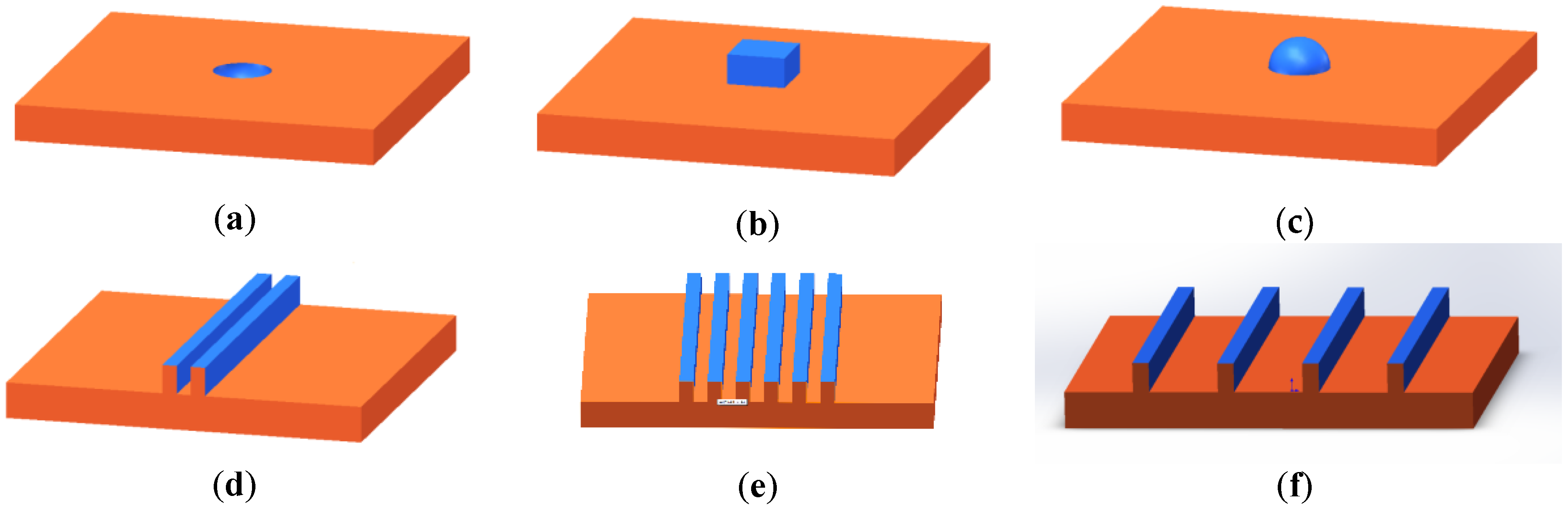
The materials of the four targets were all silicon, and the target structures are demonstrated in
Figure 2, where different colors are used to highlight their structural features. Each model was illuminated by two kinds of light waves with the electric vector perpendicular or parallel to the incident plane. The structure of the first three targets was centrosymmetric, that is, the structures were consistent along
X- and
Y-axes, whereas the structure of the last target was center asymmetric. For convenience, the lines of the silicon line array were oriented perpendicular to the incident plane, so the porization of illumination light could be described as either perpendicular (0° polarization) or parallel (90° polarization) to the silicon lines.
3.2. Simulation Procedure
The complete simulation was separated into three parts. In the first part, the interaction between the light wave and target was calculated with the FDTD method. In this part, the scattering matrix depicted in Equation (16) is expected to be derived. The scattering matrix is dependent only on the simulated structure and wavelength of light, and it describes the complete interaction with two illumination polarizations. In the second part, an in-focus image and a set of defocused images were simulated by changing the value of in Equation (14). In the last part, a TSOM image was obtained using a particular method.
Attota et al. proposed the details of obtaining both the simulated and experimental TSOM images [
10], and the procedure is restated below for convenience.
Obtain an in-focus image and a series of defocused images of the target and a smooth background surface, respectively, as they are scanned along the axis direction.
Normalize each through-focus image of the target and background as follows:
For the in-focus or each defocused position, directly subtract the normalized background image from the normalized target image.
Select the inspection region with a strip window on the subtracted normalized image at each focus height, and extract the intensity profile by averaging the image intensity along the width of the window.
Stack the averaged intensity profile of each subtracted normalized through-focus image according to its corresponding focus height to construct a raw TSOM image, which contains three-dimensional information. X- (horizontal), Y- (vertical), and Z-axes represent the spatial position across the target, the focus position, and the optical intensity, respectively.
Interpolate and smooth the raw TSOM image and add pseudo color. The result is the final TSOM image needed.
3.3. Simulation Results
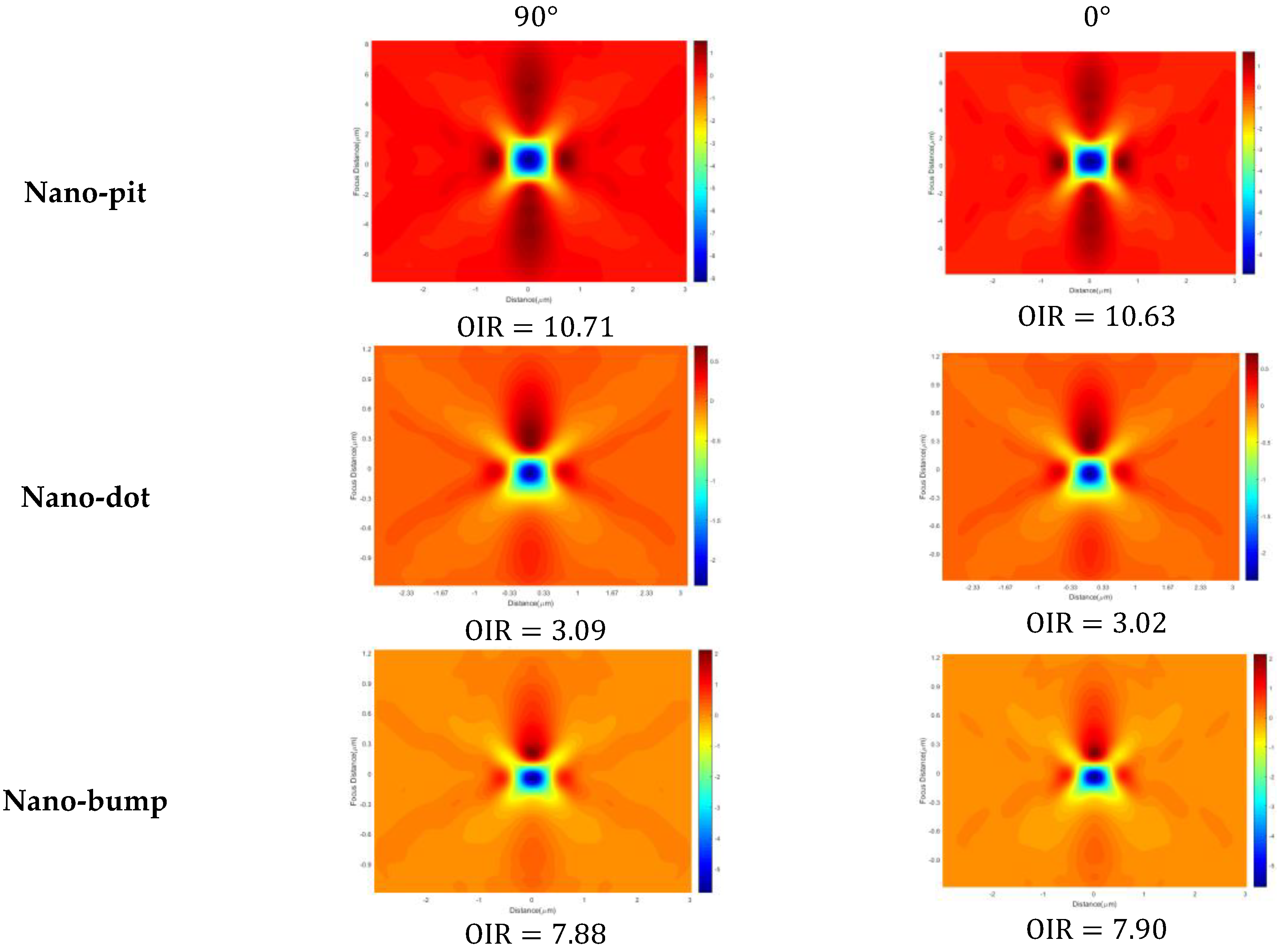
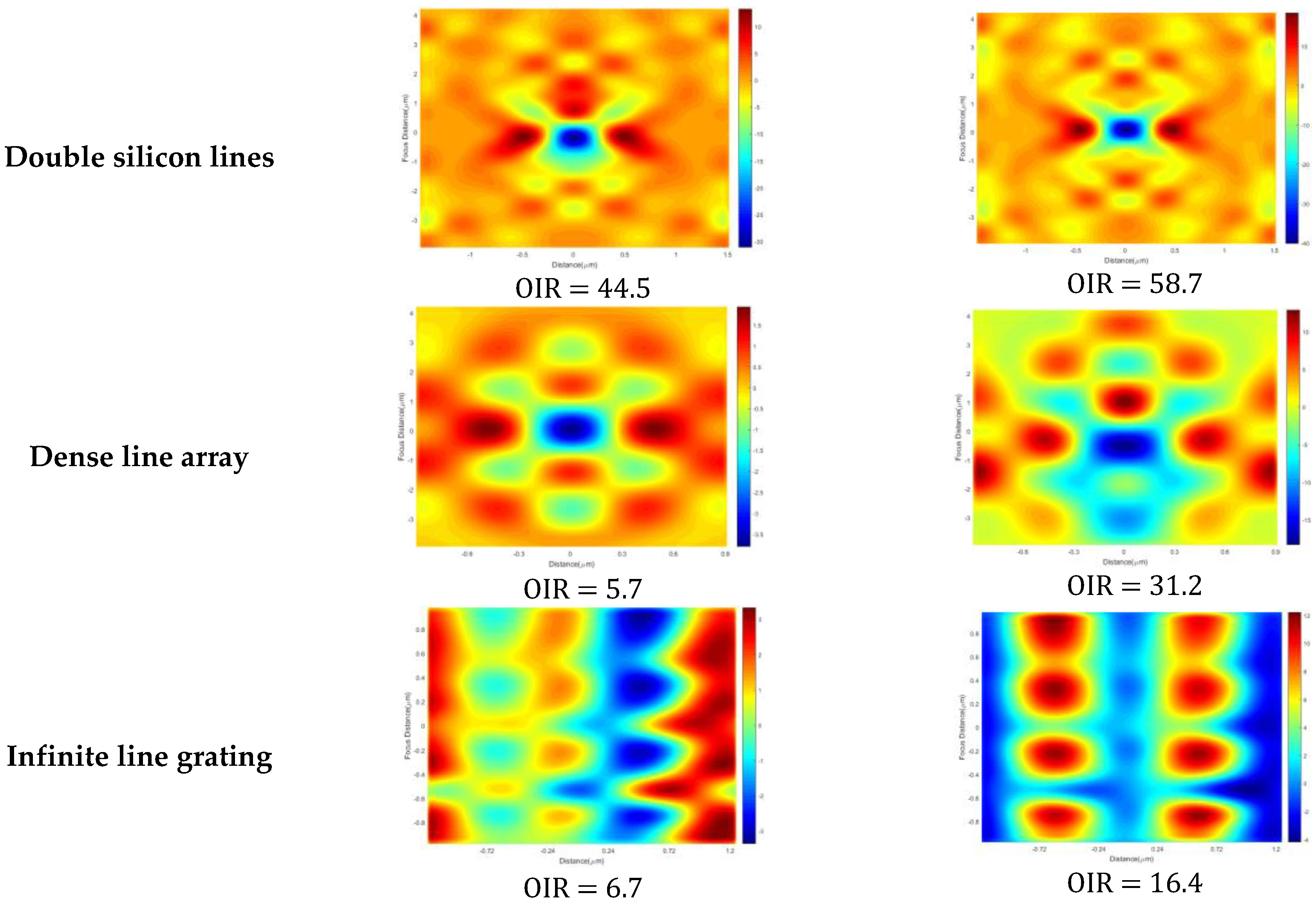
The simulated TSOM images of the six targets in the illumination polarizations of 90° and 0° are illustrated in
Figure 3. The relative difference of OIR (
) is calculated in Equation (19).
The first three targets were centrosymmetric. Under this condition, their TSOM images appear to be qualitatively similar. The corresponding OIRs in the two illumination polarizations were not strongly different, which illustrates a weak influence of polarization on the sensitivity of TSOM with regards to the targets of centrosymmetric features.
The others were center asymmetric, that is, the silicon lines were oriented parallel to the Y-axis, but periodic along the X-axis. Under this condition, an apparent influence of illumination polarization on the sensitivity of TSOM can be observed as the two TSOM images and corresponding OIRs were strongly different.
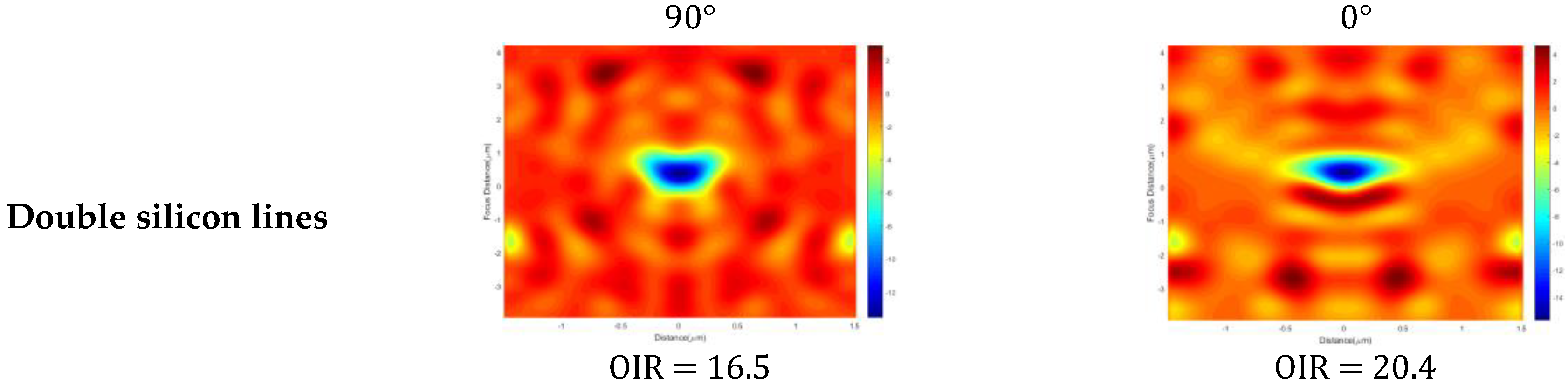
The effect brought about by illumination numerical aperture (INA) was also studied by simulating the TSOM of the double silicon line upon setting INA = 0.8 and keeping other parameters in line with those in the previous simulation.
Figure 4 presents the simulation results.
By comparing the results of
Figure 3 and
Figure 4, it is demonstrated that the OIR of the TSOM image with the illumination numerical aperture of 0.8 is smaller than that with the illumination numerical aperture of 0.4. However, the two corresponding OIRs in both illumination polarizations are still different. It is concluded that the effect brought about by the illumination polarization and the target structural feature exists as long as the metrology is performed in the same illuminating and imaging conditions.
To analyze this phenomenon further, the line height of the double silicon line and dense line array were increased by 10 nm, but the other parameters are kept constant. This dimensional change produced a new TSOM image. The dimensional change was highlighted by a simple subtraction of the new and previous TSOM images and illustrated in a differential TSOM (DTSOM) image. The inspection of the vertical sensitivity of the dimensional change was directly quantified by the OIR of the DTSOM image. The DTSOM images in the two illumination polarizations are shown in
Figure 5. The relative difference of OIR is provided in
Table 3.
4. Experiment
4.1. Experimental Set-Up
The optical scheme of the experiment is shown in
Figure 6. A Zeiss Axio Imager M2 was used as the inspection device. The illumination numerical aperture (INA) and collection numerical aperture (CNA) were both 0.8, and the magnification of the objective was 100×. The wavelength of illumination light was 555 nm. The optical path of illumination was designed as a Köhler illumination with a polarizer to produce the two kinds of linear polarizations mentioned above. A motor stage in closed-loop control was located beneath the microscope. The in-focus image and defocused images were collected by moving the motor stage vertically.
4.2. Experimental Sample
Two Au line arrays deposited on smooth silicon substrates were inspected. The line heights of the array were 50 nm and 70 nm, and the width of each Au line was approximately 20 nm. Each array was separated into 10 groups, and the nominal pitch of each group decreased from 1000 nm to 50 nm. The SEM of one Au line array is presented in
Figure 7.
4.3. Experimental Results
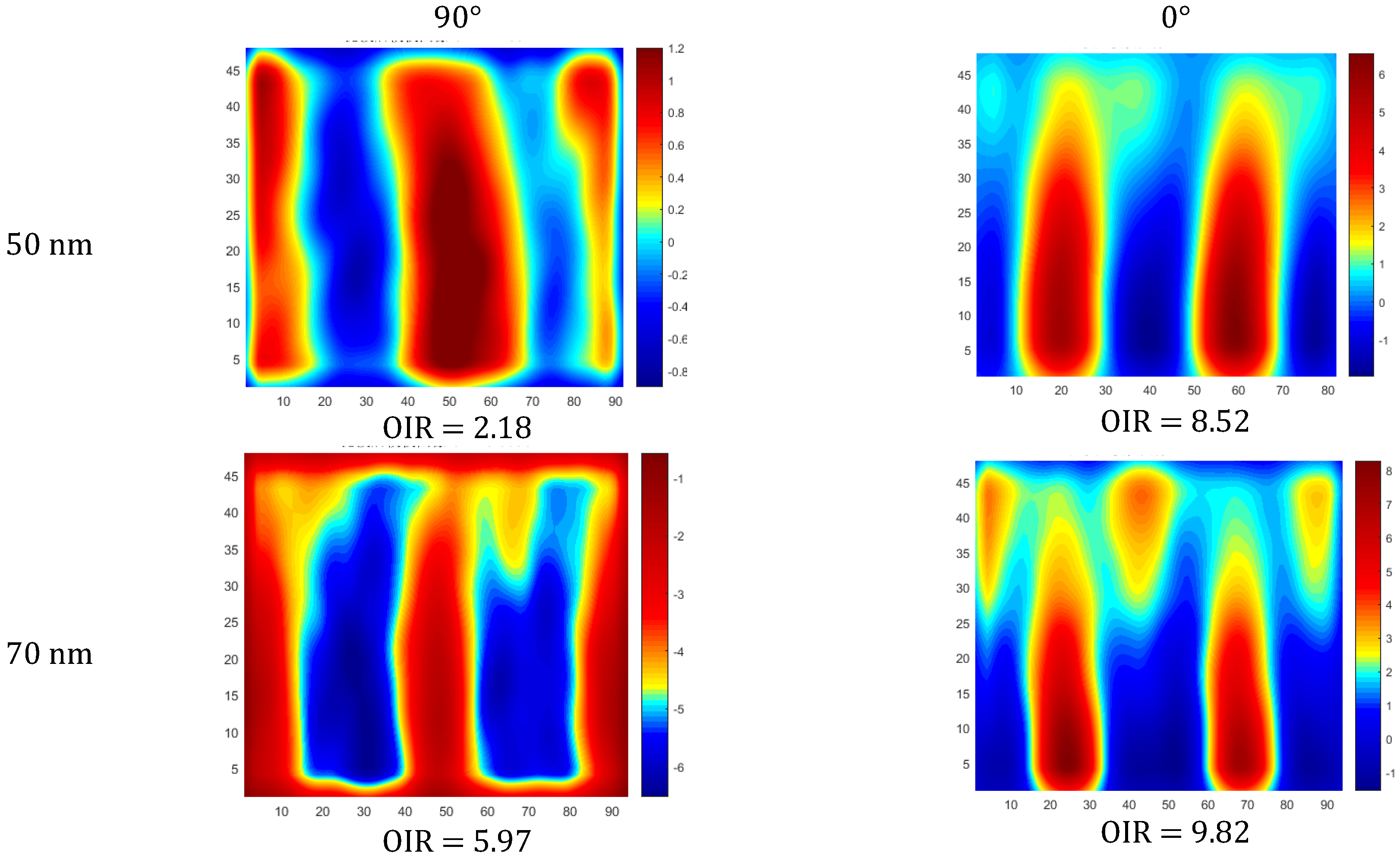
To verify our analysis and prove the effects of illumination polarization and structural features, the Au line array with the pitch of 1000 nm was inspected using TSOM with two illumination polarizations.
Figure 8 presents the simulation results of the Au line array with 50-nm height. The TSOM images were simulated with a 0.8 INA, 0.8 CNA, and 555-nm illumination wavelength, which was identical to the experimental conditions.
Figure 9 shows the experimental results of the Au line arrays with 50-nm and 70-nm height.
The microscope system noise is dependent on the stray light, blurs on the wafer, aberration of the microscope, and imprecision of the motion and location component of the stage [
2,
15]. The TSOM images of the system noise with two illumination polarizations were obtained by subtracting two background TSOM images corresponding to line heights of 70 nm and 50 nm. The TSOM images are demonstrated in
Figure 10.
Clearly, the intensity of signal and system noise are quantified by the OIR of the TSOM images of the target and noise, respectively. By dividing the OIR of the TSOM image of the target by that of the TSOM image of the noise, the signal-to-noise ratio (SNR) of TSOM is retained. The SNRs in the two illumination polarizations are presented in
Table 4. According to the result, for the given target, the sensitivity and SNR apparently increase when the polarization is perpendicular to the Au lines.
5. Analysis and Discussion
When light is scattered from the targets, its amplitude is changed. These changes depend on the sample material and shape, as well as the illumination polarization. As mentioned in
Section 3.1, the structural features of nano-pit, nano-dot, and nano-bump were centrosymmetric. According to the analysis in
Section 2, the function of their effective refractive index is also centrosymmetric, that is, in the polar coordinate
Therefore, the effective refractive indices of these three targets are constant with respect to the two illumination polarizations. For the silicon or Au lines, the function of the equivalent refractive index along the horizontal (X) axis is inconsistent but periodic. From the simulation and experimental results, the TSOM image and its OIR of the centrosymmetric targets is similar regardless of the different illumination polarizations, but an apparent difference can be observed for center asymmetric targets, which supports our hypothesis.
From the data of the last three rows of
Table 2 and the data of
Table 3 (double silicon lines and dense line array), the relative differences between OIRs of TSOM and DTSOM increase as the number of lines increases or the pitch of the array decreases. This phenomenon can be explained through the effect of form birefringence, which leads to two effective refractive indices for two orthogonal polarizations. The form birefringence strongly depends on the sample structure even if the sample material is non-birefringent. As the number of lines increases or the pitch of the array decreases, the scattered light intensity of the perpendicular polarization varies more significantly across the line and space than that of the parallel polarization, which is eventually illustrated through the relative difference between OIRs with the two illumination polarizations.
6. Conclusions
In this study, the complete image-forming procedure of TSOM was modeled, and it included Köhler illumination in the TSOM, the scattered electromagnetic field reflected from a complex target, and the image-scanning procedure. The FDTD method was performed to simulate the TSOM images of four targets with representative structural features, and the OIRs with two illumination polarizations were analyzed. The simulation and experimental results demonstrate that, for centrosymmetric targets, neither of the polarizations is effective for improving inspection sensitivity and SNR. On the contrary, for the asymmetric targets such as silicon and Au line arrays, the sensitivity and SNR apparently improved when the illumination polarization light was perpendicular to the lines. This result is valuable in TSOM applications for micro- and nano-inspection by saving time and improving measuring efficiency and precision.
Author Contributions
Conceptualization, Y.Q. and R.P. Methodology, J.J. Software, R.P. Validation, Y.Q., R.P., and J.H. Formal analysis, R.P. Investigation, R.P. Resources, H.P. and J.N. Data curation, R.P. Writing—original draft preparation, Y.Q. and R.P. Writing—review and editing, Y.Q. Visualization, R.P. Supervision, Y.Q. Project administration, Y.Q. Funding acquisition, Y.Q.
Funding
This research was funded by the Natural National Science Foundation of China (NSFC) No. 51675033.
Conflicts of Interest
The authors declare no conflicts of interest.
References
- Ravikiran, A.; Ronald, G.D.; John, A.K.; James, E.P.; András, E.V.; Benjamin, B.; Erik, N.; Andrew, R. TSOM method for semiconductor metrology. Metrol. Insp. Process Control Microlithogr. 2011. [Google Scholar] [CrossRef]
- Ravikiran, A. Noise analysis for through-focus scanning optical microscopy. Opt. Lett. 2016, 41, 745–748. [Google Scholar]
- Jun, H.L.; Jun, H.P.; Dohwan, J.; Eun, J.S.; Chris, P. Tip/tilt-compensated through-focus scanning optical microscopy. Opt. Metrol. Insp. Ind. Appl. IV 2016. [Google Scholar] [CrossRef]
- An-Shun, L.; Yi-Sha, K.; Nigel, S. Through-focus technique for overlay metrology. Metrol. Insp. Process Control Microlithogr. XXI 2007. [Google Scholar] [CrossRef]
- Timothy, F.C. Defect metrology challenges at the 11-nm node and beyond. Metrol. Insp. Process Control Microlithogr. XXIV 2010. [Google Scholar] [CrossRef]
- Golani, O.; Dolev, I.; Pond, J.; Niegemann, J. Simulating semiconductor structures for next-generation optical inspection technologies. Opt. Eng. 2016, 55, 025102. [Google Scholar] [CrossRef]
- Ryoichi, H.; Nobutaka, K.; Hideaki, H.; Kenichi, T.; Masatoshi, H.; Hiroyuki, S. Study of EUV mask inspection technique using DUV light source for hp22nm and beyond. Photomask Technol. 2010. [Google Scholar] [CrossRef]
- Bryan, M.B.; Richard, Q.; Yeung-Joon, S.; Hui, Z.; Richard, M.S. Optical illumination optimization for patterned defect inspection. Metrol. Insp. Process Control Microlithogr. XXV 2011. [Google Scholar] [CrossRef]
- Stover, J.C. Optical Scattering Measurement and Analysis, 3rd ed.; SPIE Press: Bellingham, WA, USA, 2012; pp. 91–108. [Google Scholar]
- Ravikiran, A.; Hyeonggon, K. Parameter optimization for through-focus scanning optical microscopy. Opt. Express 2016, 24, 14915–14924. [Google Scholar]
- Ravikiran, A.; Peter, W.; John, A.K.; Bunday, B.; Victor, H.V. Feasibility study on 3-D shape analysis of high-aspect-ratio features using through-focus scanning optical microscopy. Opt. Express 2016, 24, 16574–16585. [Google Scholar]
- Jérôme, V.A.; Flavien, H.; Adam, C.; James, P. Uniform illumination and rigorous electromagnetic simulations applied to CMOS image sensors. Opt. Express 2007, 15, 5494–5503. [Google Scholar]
- Yeung, J.S.; Brian, M.B.; Lowell, H.; Richard, M.S.; Ravikiran, A.; Michael, T.S. Köhler illumination in high-resolution optical metrology. Metrol. Insp. Process Control Microlithogr. XX 2006. [Google Scholar] [CrossRef]
- Marx, B.; Emil, W. Principles of Optics, 7th ed.; Publishing House of Electronics Industry: Beijing, China, 2009; pp. 608–613. [Google Scholar]
- Ryabko, M.; Koptyaev, S.; Shcherbakov, A.; Lantsov, A.; Oh, S.Y. Motion-free all optical inspection system for nanoscale topology control. Opt. Express 2014, 22, 14958–14963. [Google Scholar] [CrossRef] [PubMed]
Figure 1.
Schematic of (a) illumination numerical aperture (INA; red) and (b) collection numerical aperture (can; blue).
Figure 1.
Schematic of (a) illumination numerical aperture (INA; red) and (b) collection numerical aperture (can; blue).
Figure 2.
Computer-aided design (CAD) models for (a) nano-pit, (b) nano-dot, (c) nano-bump, (d) double silicon lines, (e) dense line array, and (f) infinite line grating.
Figure 2.
Computer-aided design (CAD) models for (a) nano-pit, (b) nano-dot, (c) nano-bump, (d) double silicon lines, (e) dense line array, and (f) infinite line grating.
Figure 3.
Simulated through-focus scanning optical microscopy (TSOM) images of the six targets with different structural features with illumination polarizations of 90° (the first column) and 0° (the second column); OIR—optical intensity range; INA = 0.4.
Figure 3.
Simulated through-focus scanning optical microscopy (TSOM) images of the six targets with different structural features with illumination polarizations of 90° (the first column) and 0° (the second column); OIR—optical intensity range; INA = 0.4.
Figure 4.
Simulated TSOM images of double silicon lines with illumination polarizations of 90° (the first column) and 0° (the second column); INA = 0.8.
Figure 4.
Simulated TSOM images of double silicon lines with illumination polarizations of 90° (the first column) and 0° (the second column); INA = 0.8.
Figure 5.
Simulated differential TSOM (DTSOM) images for silicon line array with illumination polarizations of 90° (the first column) and 0° (the second column). The line height was increased by 10 nm, but the line width and pitch were kept constant.
Figure 5.
Simulated differential TSOM (DTSOM) images for silicon line array with illumination polarizations of 90° (the first column) and 0° (the second column). The line height was increased by 10 nm, but the line width and pitch were kept constant.
Figure 6.
Schematic of the TSOM nanoscale metrology device, where the red ray is the illumination ray and the green ray is the imaging ray. The INA of the illuminating system is defined by the iris and the CNA of imaging system is defined by the objective. The motor stage and charge-coupled device (CCD) were controlled by a computer so that the CCD took one picture as soon as the motor stage moved a certain distance.
Figure 7.
SEM of Au line array. In this figure, the width of the Au line is 23.6 nm, and the pitch of this group is approximately 1000 nm.
Figure 7.
SEM of Au line array. In this figure, the width of the Au line is 23.6 nm, and the pitch of this group is approximately 1000 nm.
Figure 8.
Simulated TSOM images of Au line arrays with illumination polarizations of 90° (a) and 0° (b).
Figure 8.
Simulated TSOM images of Au line arrays with illumination polarizations of 90° (a) and 0° (b).
Figure 9.
Experimental TSOM images for the Au line arrays with illumination polarizations of 90° (the first column) and 0° (the second column). The line heights were 50 nm and 70 nm.
Figure 9.
Experimental TSOM images for the Au line arrays with illumination polarizations of 90° (the first column) and 0° (the second column). The line heights were 50 nm and 70 nm.
Figure 10.
Experimental TSOM images of the system noise with 90° polarization (a) and 0° polarization (b).
Figure 10.
Experimental TSOM images of the system noise with 90° polarization (a) and 0° polarization (b).
Table 1.
Structure and imaging parameters used in the simulation.
Table 1.
Structure and imaging parameters used in the simulation.
| Target | Structure Parameter | Imaging Parameter |
|---|
| Illumination Numerical Aperture | Collection Numerical Aperture | Wavelength (nm) |
|---|
| Nano-pit | Radius | 100 nm | 0.4 | 0.8 | 546 |
| Nano-dot | Length | 121 nm | 0.4 | 0.8 | 546 |
| Width | 121 nm |
| Height | 71 nm |
| Nano-bump | Radius | 100 nm | 0.4 | 0.8 | 546 |
| Double silicon lines | Width | 30 nm | 0.4 | 0.8 | 546 |
| Height | 50 nm |
| Pitch | 20 nm |
| Sidewall angle | 90° |
| Dense line arry | Width | 30 nm | 0.4 | 0.8 | 546 |
| Height | 50 nm |
| Pitch | 60 nm |
| Sidewall angle | 90° |
| Infinite line grating | Width | 30 nm | 0.4 | 0.8 | 546 |
| Height | 50 nm |
| Pitch | 600 nm |
| | Sidewall angle | 90° |
Table 2.
Relative difference between optical intensity ranges (OIRs) with two illumination polarizations. TSOM—through-focus scanning optical microscopy.
Table 2.
Relative difference between optical intensity ranges (OIRs) with two illumination polarizations. TSOM—through-focus scanning optical microscopy.
| Targets | Relative Difference (TSOM) |
|---|
| Nano-pit | 0.74% |
| Nano-dot | 2.3% |
| Nano-bump | 0.25% |
| Double silicon lines | 31.9% |
| Dense line array | 447% |
| Infinite line grating | 145% |
Table 3.
Relative difference between OIRs with two illumination polarizations. DTSOM—differential TSOM.
Table 3.
Relative difference between OIRs with two illumination polarizations. DTSOM—differential TSOM.
| Target | Relative Difference (DTSOM) |
|---|
| Double silicon lines | 62.9% |
| Dense line array | 203% |
Table 4.
Signal-to-noise ratio (SNR) of each Au line array with different illumination polarizations.
Table 4.
Signal-to-noise ratio (SNR) of each Au line array with different illumination polarizations.
| Line Height | 90° Polarization | 0° Polarization |
|---|
| 50 nm | SNR = 2.47 | SNR = 8.45 |
| 70 nm | SNR = 6.47 | SNR = 9.62 |
© 2018 by the authors. Licensee MDPI, Basel, Switzerland. This article is an open access article distributed under the terms and conditions of the Creative Commons Attribution (CC BY) license (http://creativecommons.org/licenses/by/4.0/).


