Shape Mapping Detection of Electric Vehicle Alloy Defects Based on Pulsed Eddy Current Rectangular Sensors


1
Automotive & Transportation Engineering, Shenzhen Polytechnic, Shenzhen 518055, China
2
College of Electrical & Information Engineering, Hunan University, Changsha 410082, China
*
Authors to whom correspondence should be addressed.
Appl. Sci. 2018, 8(11), 2066; https://doi.org/10.3390/app8112066
Submission received: 28 September 2018
/
Revised: 14 October 2018
/
Accepted: 22 October 2018
/
Published: 26 October 2018
(This article belongs to the Special Issue Nondestructive Testing and Imaging Based on Electromagnetic Fields and Waves)
Abstract
:In this paper, we investigate pulsed eddy current (PEC) testing based on a rectangular sensor for the purpose of defect shape mapping in electric vehicle lightweight alloy material. Different dimensional defects were machined on the 3003 aluminum alloy and detected using the A-scan technique and C-scan imaging in two scanning directions. The experiment results indicated that defect plane shape could be preliminarily obtained and length and width could be estimated based upon C-scan contour images. Consequently, the comparison of results between the two directions showed that the C-scan identification in the direction of magnetic flux was better than in the direction of the exciting current. Finally, subsurface defects and irregular defects were detected to verify the performance of shape mapping as a recommended approach. The conclusion drawn indicates that the proposed method, based on PEC rectangular sensors, is an effective approach in reconstructing a defect’s shape.
1. Introduction
In order to make power lithium-ion battery systems for electric vehicles with higher energy densities, a significant amount of aluminum alloy and composite materials are used in the battery shell. As an important material in electric vehicle power batteries, shells, and cover plates, 3003 aluminum alloy plays an important role in new energy vehicles. However, corrosion, wear, and other defects that may occur during the use of this material pose a serious threat to safety, making it necessary to find defects quickly and accurately in order to avoid great losses.
Pulsed eddy current (PEC) testing is a nondestructive and effective electromagnetic inspection technique [1,2,3,4,5,6,7]. PEC testing exhibits many advantages over conventional nondestructive testing (NDT). First of all, as opposed to ultrasonic inspection, PEC testing does not require an acoustic couplant, so it does not pollute the material being tested. Moreover, PEC testing can detect deeper defects than infrared and thermal NDT, which is normally used to detect shallow defects [8]. In addition, PEC testing is more economical and less hazardous than radiography inspection [9]. PEC testing has more advantages than ordinary eddy current (EC) testing, such as: a deeper detection depth [10], easier generation and control [11,12], and richer information in frequency domains. Therefore, it is widely used not only for the measurement of the conductivity and thickness of metal [13], but also in defect characterization [14,15,16,17,18]. In fact, this nondestructive testing method can not only detect the surface defects and subsurface defects of stainless steel materials [19], but also of nonferrous metal materials such as aluminum, magnesium and its alloy materials [20,21,22,23,24], and carbon fiber reinforced plastics (CFRPs) [25].
The probe in EC testing is usually comprised of excitation and detection units. The excitation unit inducing the eddy current in materials being tested is usually a cylindrical coil [26,27,28,29,30,31,32]. As a comparison, a rectangular coil can induce uniform and unidirectional eddy currents in the detected material, and has been devised particularly for EC testing [33] and alternating current field measurement (ACFM) testing [34]. In 2006, a rectangular coil was proposed and researched in PEC testing [10,35]. In 2010, the defect classification and defect edge identification were studied using a rectangular PEC sensor [36,37]. In 2012, a study showed that a rectangular sensor can induce a uniform eddy current on aluminum plates and that the size of a crack can be quantitatively detected by analyzing the three signals (Bx, By, and Bz) [38]. The author and his team proposed a PEC method based on a rectangular excitation coil (REC) and an axial parallel pickup coil for metal loss evaluation and imaging [23,39]. This article is the continuation and expansion of the original research. However, the detection coil used the most in all of these studies was a Bz pickup coil, which is orthogonal to an REC and a specimen. In 2009, three-dimensional detection coils (Bx, By, and Bz) were investigated to detect the magnetic field of an eddy current induced by rectangular coil and to identify the defect. The experimental results showed that three-dimensional detection coils could obtain more information about defect sizing than uniaxial coils (Bz) [36], yet the study did not go deep into the field of imaging. A By pickup coil orthogonal to an REC and parallel to a specimen—which may have the potential to discover plane shape defect—has not been researched until now. Therefore, this paper mainly studies a PEC detection method based on a rectangular coil and a By pickup coil for mapping a plane shape defect. Previous research on pulsed eddy current detection involved the z-axis, and the authors’ earlier paper focused on the x-axis. The novelty of this paper is reflected in the fact that it studies the magnetic field of the coil along the y-axis.
2. Problem Statement
Since imaging techniques can obtain the shape of a defect, they are more intuitive than ordinary A-scan and B-scan techniques. For the last few years, some eddy current testing was investigated and combined with imaging techniques to detect and evaluate defects, such as PEC C-scan imaging [5,40], electromagnetic tomography (EMT) [41,42], eddy current thermography [43], and magneto-optical imaging [44,45,46]. The C-scan imaging technique has several advantages such as a low cost, easy control, and automatization. A detailed application of the C-scan technique for aluminum alloy plates and a comparison with the A-scan technique is described in References [47,48,49]. Therefore, most defect shape mapping in this paper is completed by the PEC C-scan imaging technique.
The rest of this article is organized as follows. First, the PEC rectangular excitation coil and By pickup coil are introduced in Section 3.1. Then, the experimental setup and specimens developed in our laboratory are shown in Section 3.2. Then, the curves of the A-scan’s peak are analyzed at the beginning of Section 4. Defect shape mapping based on C-scan imaging is investigated in the rest of Section 4. Finally, conclusions are outlined in Section 5.
3. Detection Method
3.1. Rectangular Sensor
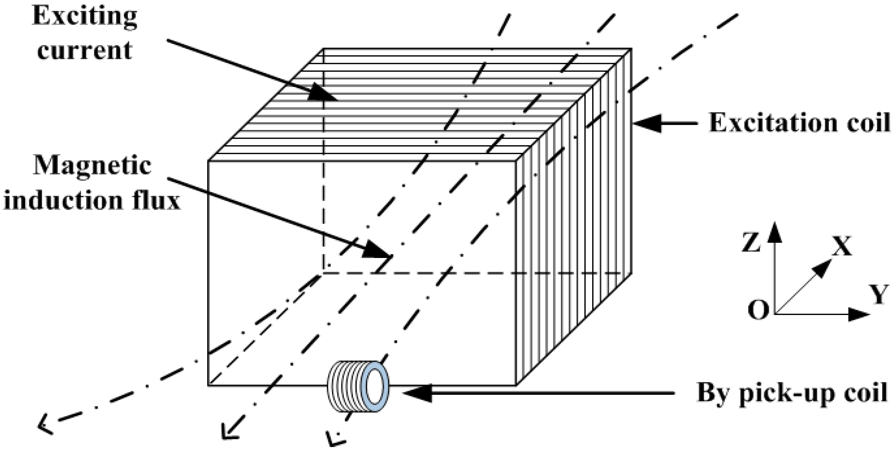
The PEC rectangular sensor in this work consisted of a rectangular coil and a By pickup coil. As shown in Figure 1, a Cartesian coordinate system was established. The normal of the excitation coil was parallel to the x-axis, while the normal of the By pickup coil was parallel to the y-axis. In other words, the excitation coil was orthogonal to the By pickup coil. The By pickup coil located at the bottom-center of the REC could measure the changing rate of the By component of the magnetic field. The REC was 45 mm in width, 50 mm in length, and 45 mm in height [28,29,30,44]. The lift-off distance of the probe was 0.5 mm, which is a constant in a scanning experiment. The other parameters of the REC and the By pickup coil are shown in Table 1.
In previous work, PEC rectangular sensor scanning was performed along two directions: one in the direction of magnetic flux and the other in the direction of the excitation current [10,29,30]. The direction of magnetic flux was parallel to the x-axis while the direction of the excitation current was parallel to the y-axis [37]. Here, defect shape mapping experiments were carried out in both directions [23].
3.2. Experiment Setup
The experimental device contained an excitation module, a signal-conditioning module, and an analog-to-digital converter module. The excitation pulse generated and enhanced by the excitation module was driven into the rectangular coil. The signal-conditioning module was used to amplify the response signal measured by the pickup coil, while the data acquisition module was used to sample the signal [10,37].
3.3. Experiment Specimen and Conditions
There were four pieces of specimens made up of 3003 aluminum-manganese (Al-Mn) alloy with a conductivity of 50%–55% IACS. The first and second specimens were 200 mm in width, 200 mm in length, and 2 mm in thickness. On the surface of each specimen, an electron discharge machining (EDM) slot was fabricated to simulate the corrosion type of the defects in real cases. Therefore, the size of the groove was larger than that of the crack type. The first defect (defect 1) was 5 mm in width, 15 mm in length, and 1.5 mm in depth. The second defect (defect 2) was 2.5 mm in width, 15 mm in length, and 1.5 mm in depth. The third specimen was 200 mm in length, 200 mm in width, and 3 mm in thickness. This was designed to provide for defect 3, which was 15 mm in length, 1 mm in width, and 2 mm in depth.
In addition, the fourth specimen was 200 mm in length, 200 mm in width, and 5 mm in thickness, and was used to provide for defect 4, which was an irregular surface-breaking metal-loss type of defect. Figure 2 shows the planform of defect 4. The longer length L1 was 40 mm, the shorter length L2 was 20 mm, and the width W was 12 mm.
4. Experimental Results
4.1. Curves of the A-Scan’s Peak
The A-scan technique is a common and widely-used method in pulsed eddy current testing, but it can’t be used in ordinary eddy currents testing. The third specimen was used and detected with defect 3 in this experiment.
In this experiment, the rectangular coil driven by the excitation pulse could induce a uniform eddy current in the material being tested. First, we obtained the A-scan response to the PEC, as shown in Figure 3. Then, the peak (the maximum value, shown as the peak point in Figure 3) could be extracted from the A-scan response to form the curves of the A-scan’s peak, as seen in Figure 4 and Figure 5. In future work, other features such as rising time and time to peak will be extracted.
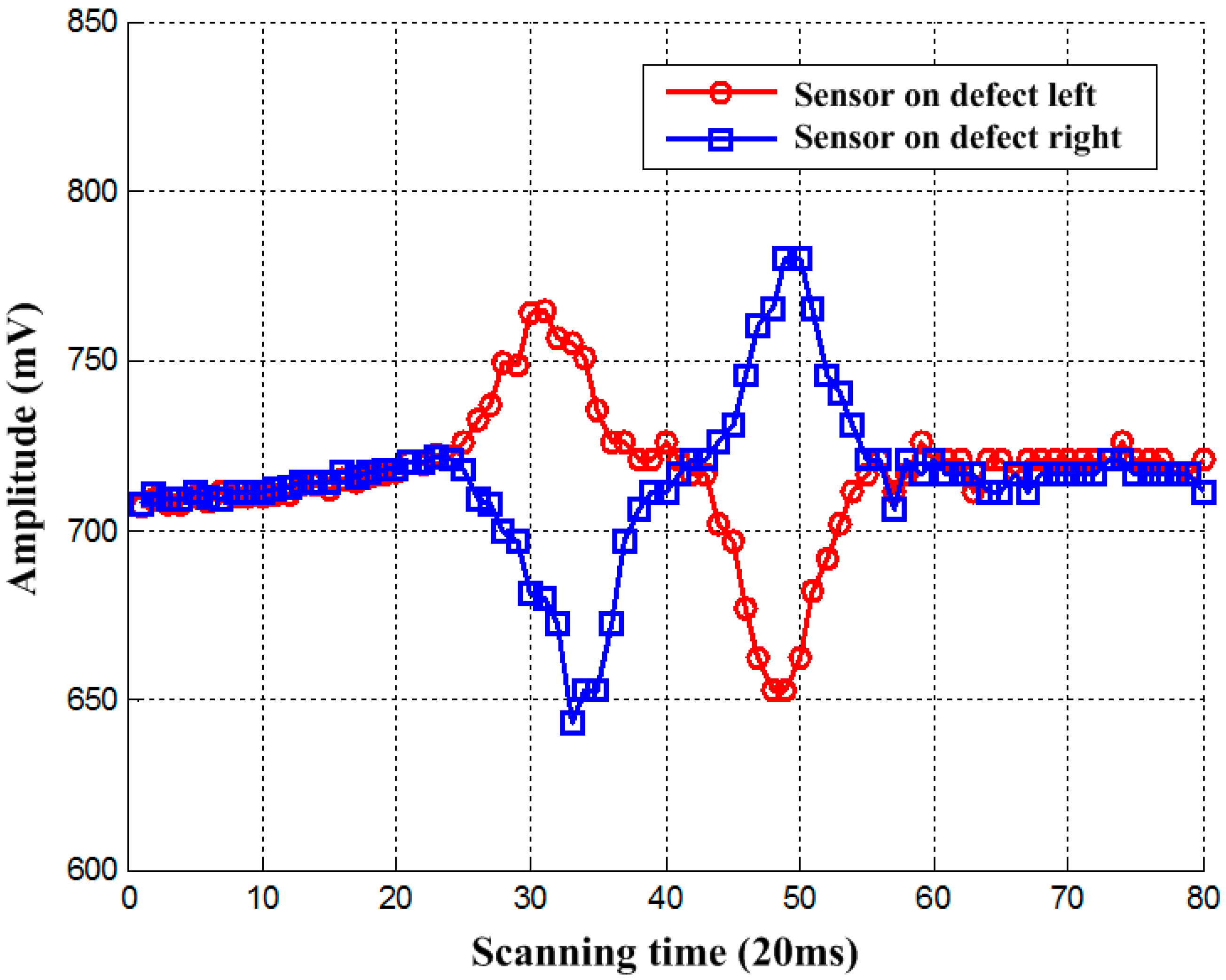
When the sensor was on the defect-free area of the specimen, the eddy currents were uniform and the curve of the A-scan’s peak measured by the By pickup coil was inherent. We suppose that there was a rectangular defect on the exterior of the specimen. When the eddy current in the specimen was disturbed by the defect, which was larger than the resistance of the specimen, the eddy current flowed to the corner of the defect. Nevertheless, the flow directions of the eddy currents in the two opposite corners were contrary. Consequently, the magnetic force induced by the changed eddy currents in the two opposite corners was also opposite. The current in the By pickup coil changed adversely when the sensor was on the opposite corner of the defect. In other words, as the probe scanned along one side (two corners) of the defect, a crest and a trough appeared in an orderly manner on the peak wave. In addition, as the probe scanned along the other side of the defect (two corners), a trough and a crest also appeared in an orderly manner on the peak wave. The maximum and minimum values of the curves on the A-scan’s peak respectively corresponded to the instant of the sensor entering and leaving the corner of the defect. This analytical result may be useful for us in imagining the defect’s shape and estimating the distance between the two corners of the defect (i.e., the length and width).
The By curves on the peak of the A-scan sensor scanning along the defect’s two sides in both directions are shown in Figure 4 and Figure 5. The horizontal axis represents scanning time, and the vertical axis represents amplitude. As can be seen from the graph, with the approaching of the defect, there were always peaks and troughs on the peak wave. On the other hand, the order of the peaks and troughs on the sensor scanning along both sides of the defect 1 was the opposite. This is in line with the analytical results in Section 3.1. The C-scan imaging technique we employed is explained next.
4.2. Defect Shape Mapping Based on C-scan Imaging
C-scan imaging software, which refers to the data acquisition software written in VC++ language, includes parameter setup, feature extraction, data acquisition, data matrix formation, data processing, and a C-scan image display. First, the excitation pulse parameters were configured in the parameter setup. In this experiment, the excitation pulse was 7.5 V in amplitude, 5 ms in pulse duration, and 100 Hz in frequency. Then, the transient response signal measured from the By pickup coil was sampled by data acquisition. Next, during feature extraction, the peak amplitude of the By transient response signal was picked up as a feature of the C-scan imaging. In data matrix formation, the coordinates of scanning points were determined and the C-scan data matrix was formed. Peak wave and transient response signals may be disturbed by unknown noise, which may lead to potential misjudgment of imaging results. With the help of the “wden” function in MATLAB, the C-scan data matrix was denoised through wavelet analysis. Finally, the data matrix was transformed to a colority matrix, and the C-scan images of the scanned area formed in step with the C-scan images display. Finally, defect shape mapping could be obtained by analyzing the C-scan images.
As described above, the data matrix needed to be denoised, and we propose wavelet analysis to denoise the C-scan data matrix during data processing. Wavelet analysis is an effective technique in signal processing, and the analysis is done in both time and frequency domains. First, the transverse data in the original C-scan data matrix was denoised. Next, the longitudinal data in the C-scan data matrix was denoised. Finally, the denoised C-scan data was transformed into a colority matrix. Figure 6 and Figure 7 display the efficiency of a two-dimensional wavelet filter, respectively showing the original C-scan contour image and the C-scan imaging results after the process of the first defect. As expected, the denoising result was clearer than the original image.
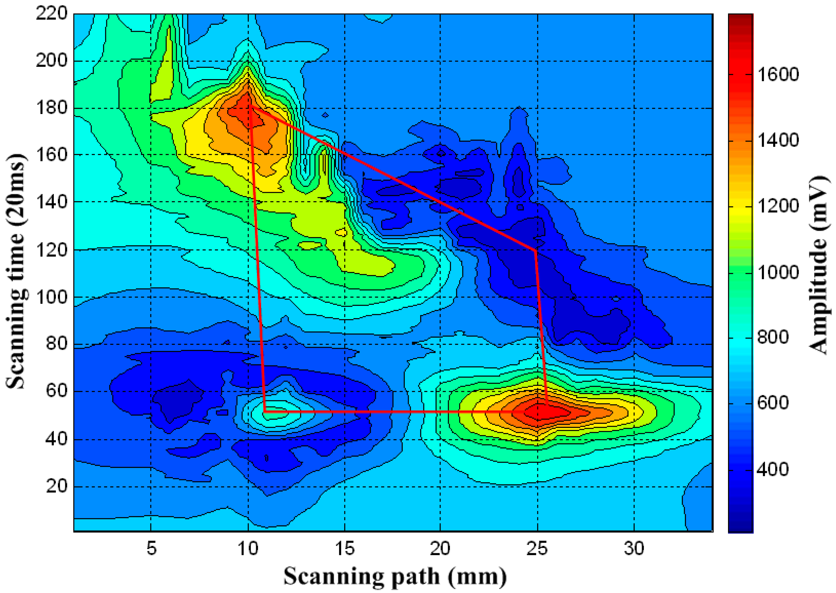
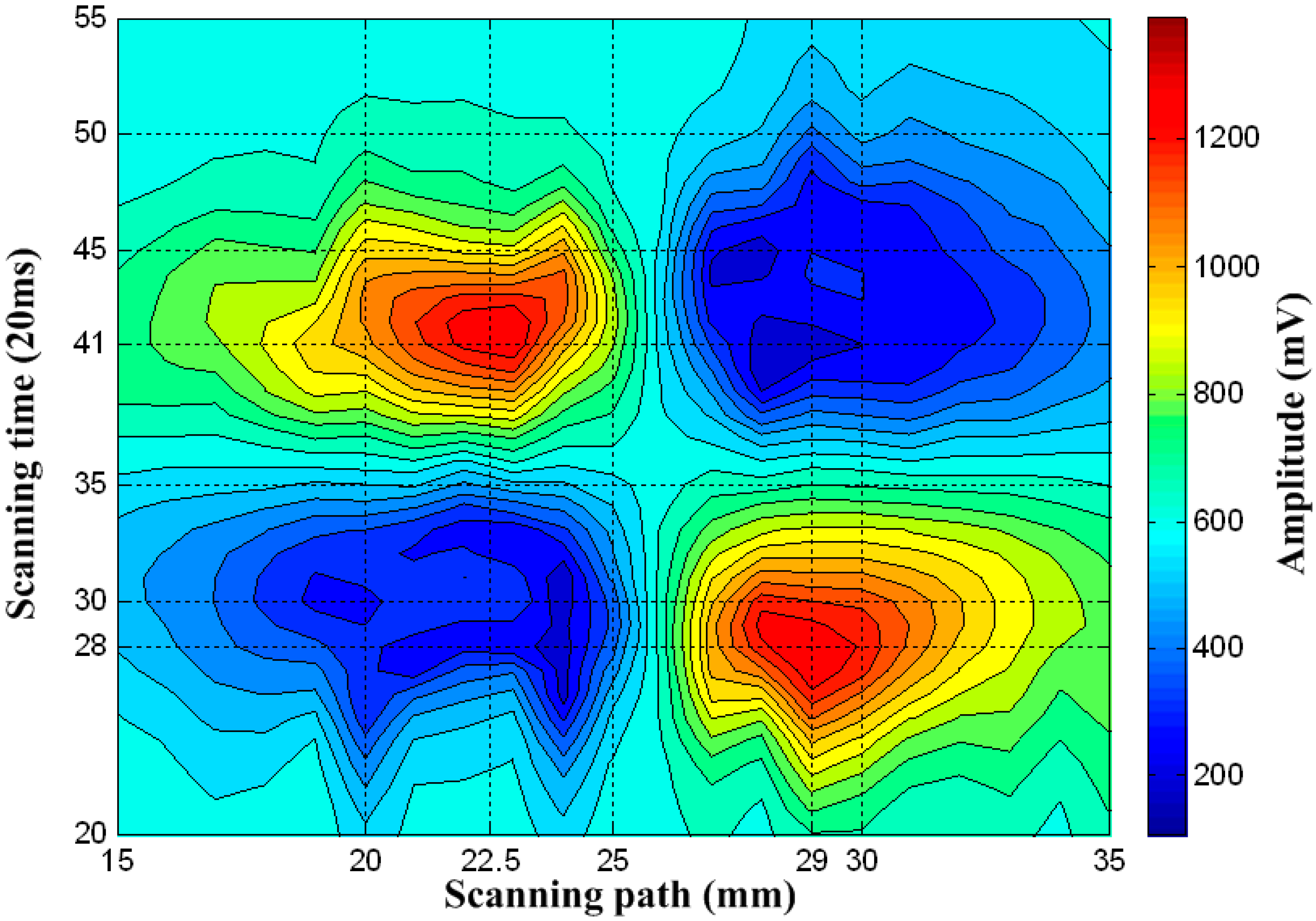
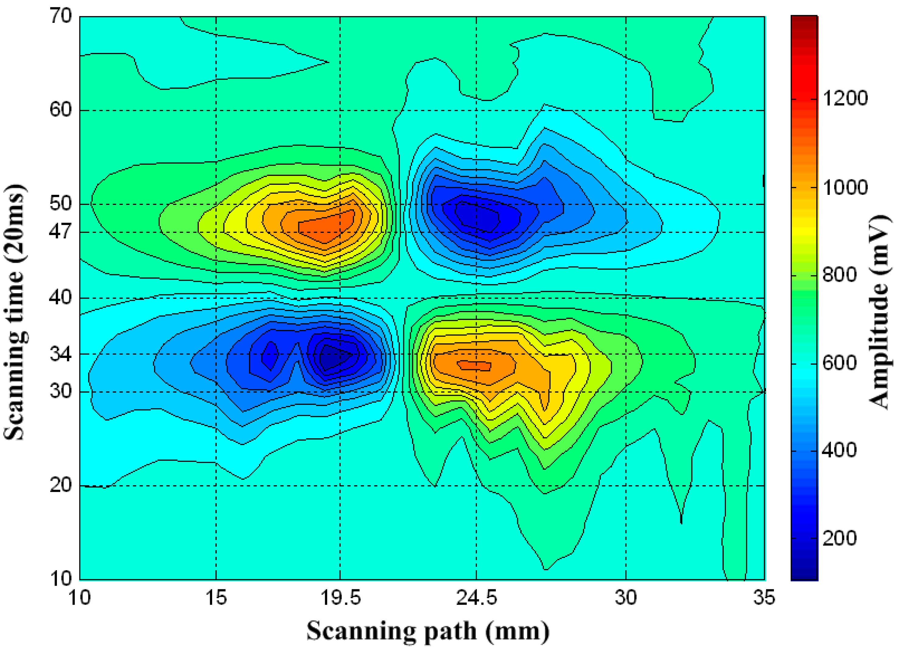
C-scan contour images of defects 1, 2, and 3 in the direction of magnetic flux are respectively shown in Figure 8, Figure 9 and Figure 10. C-scan contour images of defects one, two, and three in the direction of the exciting current are respectively shown in Figure 11, Figure 12 and Figure 13. The horizontal axis represents the scanning path, with a distance between the two adjacent scanning paths of 1 mm. The vertical axis represents the scanning time, with the color bar representing the voltage amplitude. In Figure 8, Figure 9, Figure 10, Figure 11, Figure 12 and Figure 13, two crest areas and two trough areas appear on the defect’s four corners in every C-scan contour image, which is consistent with the analysis in Section 3.1. Defects can be clearly identified and the defect’s shape can be imagined by the two crests and two troughs in the C-scan contour images.
In addition, the length of the defects can be effectively evaluated from the C-scan outline images. As shown in Figure 8, the time between the maximum and minimum values on the C-scan image corresponds to the instants when the sensor entered and left the defect angle. Defect length can be measured by the formula . Here, L is the estimated length of the defect, v is the scanning speed of the sensor, ∆t is the time difference, t2 is the time when the sensor leaves the defect corner, and t1 is the time when the sensor enters the defect corner.
The scan speed was 0.06 m/s in this experiment. The time difference of defects 1, 2, and 3 in the two directions are shown in Table 2. The preceding equation was used to calculate the size of the defects. The estimated size of the defects was slightly different from the actual size (15 mm). The width of the defects could be calculated according to the scanning path, which is shown in Table 2. Unfortunately, the estimated width was much bigger than the actual width of the defects. However, with the augmentation of the actual defect widths, the estimated width increased. From what has been discussed, we can draw the conclusion that the proposed method provides us with an effective tool to estimate the defect’s dimension.
To evaluate the performance of the methods in two directions, the results of the C-scan from the two directions were compared. Table 3 shows the maximum and minimum amplitudes of the defects in different directions. Obviously, the maximum amplitude of the defect in the direction of magnetic flux was larger than the maximum amplitude in the direction of the excitation current, and the minimum amplitude of the defect in the direction of magnetic flux was smaller than the minimum amplitude in the direction of the excitation current. In other words, defect recognition in the direction of magnetic flux was better than defect recognition in the direction of the excitation current. Therefore, defect shape mapping was only carried out in the direction of magnetic induction flux.
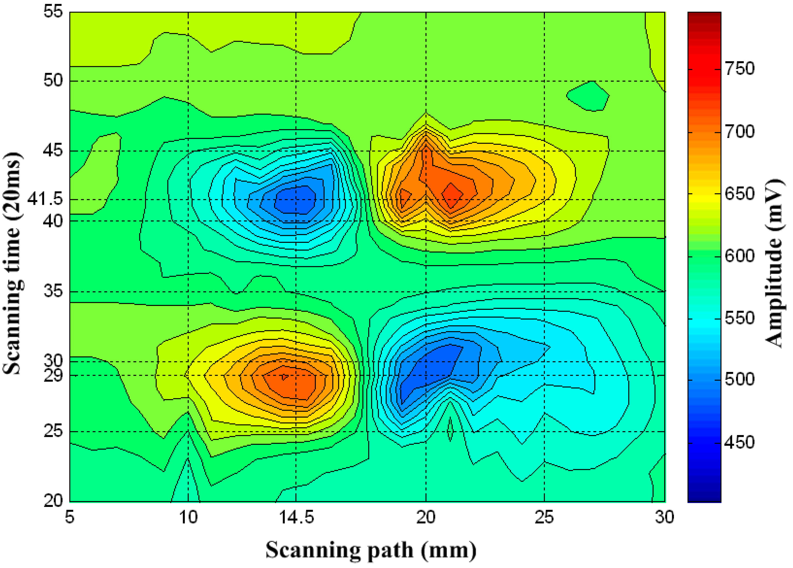
4.3. Subsurface Defect Shape Mapping
In this subsection, we describe placing the PEC sensor on the other side of the specimen to simulate a subsurface defect. Defect 1 on the subsurface was detected using the proposed method in the direction of magnetic flux. The outline image of subsurface defect 1 is shown in Figure 14. The experimental results illustrate that subsurface defect shape mapping could also be realized. According to the estimation formula for defect length, the estimated length of subsurface defect 1 was 12 mm, and the estimated width was 7.5 mm.
4.4. Irregular Defect Shape Mapping
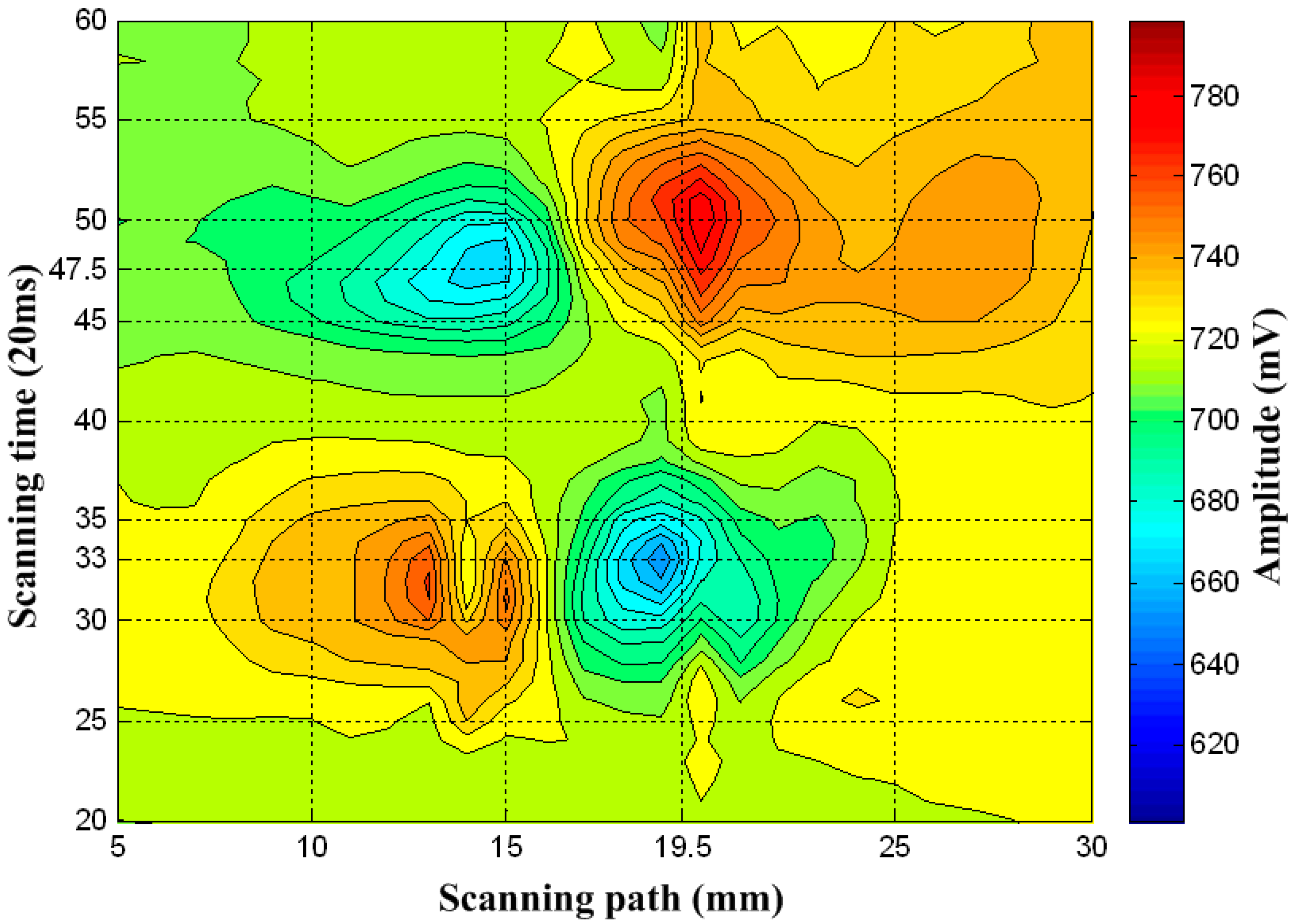
In this sub-section, we describe defect 4, which had an irregular shape. The C-scan contour image is shown in Figure 15. In the experiment, the scanning speed vx was approximately 0.015 m/s. As shown in Figure 15, the time difference between the ends of the longer length ∆t1 was approximately 2600 ms and the time difference between the ends of the shorter length ∆t2 was approximately 1300 ms. The length of the defects was calculated using the estimation formula for defect length. The estimated longer length L1 of defect 4 was 39 mm, and the estimated shorter length L2 was 19.5 mm. The estimated length was a little smaller than the actual length of defect 4 (40 mm and 20 mm). According to the scanning path, the estimated width W of defect 4 was 15 mm. The estimated width was much bigger than the actual width of defects, at 12 mm. Even with this, the shape of defect 4 could be imagined.
5. Conclusions
This paper outlines PEC detection based on rectangular coils in order to prevent accidents caused by shell defects in power-battery aluminum alloys. Defect shape mapping is realized by picking up the coil in both the direction of magnetic induction and the direction of the excitation current. Different defects developed in the 3003 Al-Mn alloy specimens. The experiment results showed that defect shape mapping in two directions could be obtained using C-scan contour images. The other finding made by this paper was that defect recognition in the magnetic induction flux direction was better than in the excitation current direction. We ascertained that the proposed method was also effective for subsurface defect and irregular defect shape mapping. One drawback in our results was that the estimated defects’ dimensions were slightly mismatched with the actual dimensions. Other than this, the proposed method, based on rectangular coils and orthogonal By pickup coils, is an effective method with which to imagine surface and subsurface defects. This may be useful in characterizing other defects with more complex geometry. The authors also acknowledge that there is still room for improvement regarding the accuracy and effectiveness of the current testing methods, which is the next step in improving the experimental system. The research team plans to use precision scanners to control the movement of sensors in subsequent experiments to reduce deviations and improve measurement accuracy. This method has potential for future applications. Moreover, this method provides a useful solution for warning of defects in the aluminum alloy shell of electric vehicle power batteries.
Author Contributions
Conceptualization, K.Z., Z.D. and Y.H.; methodology, K.Z., Z.D. and Y.H.; formal analysis, K.Z.; investigation, K.Z. and Z.Y.; resources, Z.D.; data curation, Z.Y.; writing—original draft preparation, K.Z. and Y.H.; writing—review and editing, K.Z.; visualization, Z.Y.; supervision, Y.H.; project administration, K.Z.; funding acquisition, K.Z., Z.D. and Y.H.
Funding
This work is supported by the Shenzhen Science and Technology Project (Basic Research, Grant No. JCYJ20170306144608417), National Natural Science Foundation of China (Grant No. 61501483), Shenzhen Basic Research Project (Grant No. JCYJ20160523113817077) and the Shenzhen Polytechnic Research Project (Youth Innovation, Grant No. 601822K30021).
Acknowledgments
The authors would like to extend their appreciations to the help provided by the editors and reviewers.
Conflicts of Interest
The authors declare no conflict of interest.
References
- Giguère, S.; Lepine, B.A.; Dubois, J.M.S. Pulsed eddy current technology: Characterizing material loss with gap and lift-off variations. Res. Nondestruct. Eval. 2001, 13, 119–129. [Google Scholar] [CrossRef]
- Smith, R.A.; Hugo, G.R. Deep corrosion and crack detection in aging aircraft using transient eddy-current NDE. In Proceedings of the 5th Joint NASA/FAA/DoD Aging Aircraft Conference, Orlando, FL, USA, 10–13 September 2001. [Google Scholar]
- Tian, G.Y.; Sophian, A. Defect classification using a new feature for pulsed eddy current sensors. NDT E Int. 2005, 38, 77–82. [Google Scholar] [CrossRef]
- Yong, Q.I.; Yong, L.I.; Liu, X.B.; Chen, Z.M.; Zhao, H.D. Research of pulsed eddy current testing for defect imaging based on gradient magnetic field measurement. J. Air Force Eng. Univ. 2013, 5, 63–66. [Google Scholar]
- Zhao, S.; Luo, X.; Huang, P.; Peng, X.; Hou, D.; Zhang, G. Method of imaging and evaluation for defect based on pulsed eddy current. In Proceedings of the IEEE International Instrumentation and Measurement Technology Conference, Taipei, Taiwan, 23–26 May 2016; pp. 1–6. [Google Scholar]
- Sophian, A.; Tian, G.; Fan, M. Pulsed eddy current non-destructive testing and evaluation: A review. Chin. J. Mech. Eng. 2017, 30, 500–514. [Google Scholar] [CrossRef]
- Li, J.; Wu, X.; Zhang, Q.; Sun, P. Pulsed eddy current testing of ferromagnetic specimen based on variable pulse width excitation. NDT E Int. 2015, 69, 28–34. [Google Scholar] [CrossRef]
- He, Y.; Chen, S.; Zhou, D.; Huang, S.; Wang, P. Shared excitation based nonlinear ultrasound and vibro-thermography testing for cfrp barely visible impact damage inspection. IEEE Trans. Ind. Inform. 2018. [Google Scholar] [CrossRef]
- Abidin, I.Z.; Mandache, C.; Tian, G.Y.; Morozov, M. Pulsed eddy current testing with variable duty cycle on rivet joints. NDT E Int. 2009, 42, 599–605. [Google Scholar] [CrossRef]
- He, Y.; Pan, M.; Luo, F.; Tian, G. Pulsed eddy current imaging and frequency spectrum analysis for hidden defect nondestructive testing and evaluation. NDT E Int. 2011, 44, 344–352. [Google Scholar] [CrossRef]
- Shu, L.; Huang, S.; Wei, Z.; Peng, Y. Study of pulse eddy current probes detecting cracks extending in all directions. Sens. Actuators A Phys. 2008, 141, 13–19. [Google Scholar] [CrossRef]
- Zhang, Q.; Chen, T.-L.; Yang, G.; Liu, L. Time and frequency domain feature fusion for defect classification based on pulsed eddy current NDT. Res. Nondestruct. Eval. 2012, 23, 171–182. [Google Scholar] [CrossRef]
- Yang, H.; Tai, C. Pulsed eddy-current measurement of a conducting coating on a magnetic metal plate. Meas. Sci. Technol. 2002, 13, 1259. [Google Scholar] [CrossRef]
- Tian, G.Y.; Sophian, A.; Taylor, D.; Rudlin, J. Multiple sensors on pulsed eddy-current detection for 3-D subsurface crack assessment. IEEE Sens. J. 2005, 5, 90–96. [Google Scholar] [CrossRef]
- Tian, G.Y.; Sophian, A.; Taylor, D.; Rudlin, J. Wavelet-based pca defect classification and quantification for pulsed eddy current NDT. IEE Proc. Sci. Meas. Technol. 2005, 152, 141–148. [Google Scholar] [CrossRef]
- Sambasiva Rao, K.; Mahadevan, S.; Purna Chandra Rao, B.; Thirunavukkarasu, S. A new approach to increase the subsurface flaw detection capability of pulsed eddy current technique. Measurement 2018, 128, 516–526. [Google Scholar] [CrossRef]
- Park, D.G.; Rao, B.P.C.; Vértesy, G.; Lee, D.H.; Kim, K.H. Detection of the subsurface cracks in a stainless steel plate using pulsed eddy current. J. Nondestruct. Eval. 2013, 32, 350–353. [Google Scholar] [CrossRef]
- Preda, G.; Rebican, M.; Hantila, F.I. Pulse eddy currents using an integral-fem formulation for cracks detection. Int. J. Appl. Electromagn. Mech. 2010, 333233, 1225–1229. [Google Scholar]
- Angani, C.S.; Park, D.G.; Kim, C.G.; Leela, P.; Kollu, P.; Cheong, Y.M. The pulsed eddy current differential probe to detect a thickness variation in an insulated stainless steel. J. Nondestruct. Eval. 2010, 29, 248–252. [Google Scholar] [CrossRef]
- Desjardins, D.P.R.; Krause, T.W.; Gauthier, N. Analytical modeling of the transient response of a coil encircling a ferromagnetic conducting rod in pulsed eddy current testing. NDT E Int. 2013, 60, 127–131. [Google Scholar] [CrossRef]
- Azaman, K.N.; Sophian, A.; Nafiah, F. Effects of coil diameter in thickness measurement using pulsed eddy current non-destructive testing. Mater. Sci. Eng. 2017, 260, 012001. [Google Scholar] [CrossRef]
- Xu, W.; Yang, C.; Yu, H.; Jin, X.; Guo, B.; Shan, D. Microcrack healing in non-ferrous metal tubes through eddy current pulse treatment. Sci. Rep. 2018, 8, 6016. [Google Scholar] [CrossRef] [PubMed]
- Zhang, K.; He, Y.; Dong, Z. Pulsed eddy current nondestructive testing for defect evaluation and imaging of automotive lightweight alloy materials. J. Sens. 2018, 2018, 1–11. [Google Scholar] [CrossRef]
- Garcia-Martin, J. Comparative evaluation of coil and hall probes in hole detection and thickness measurement on aluminum plates using eddy current testing. Russian J. Nondestruct. Test. 2013, 49, 482–491. [Google Scholar] [CrossRef]
- He, Y.; Tian, G.Y.; Pan, M.; Chen, D. Non-destructive testing of low-energy impact in CFRP laminates and interior defects in honeycomb sandwich using scanning pulsed eddy current. Compos. Part B 2014, 59, 196–203. [Google Scholar] [CrossRef]
- Preda, G.; Cranganu-Cretu, B.; Hantila, F.I.; Mihalache, O. Nonlinear FEM-BEM formulation and model-free inversion procedure for reconstruction of cracks using pulse eddy currents. IEEE Trans. Magn. 2002, 38, 1241–1244. [Google Scholar] [CrossRef]
- Kim, J.; Yang, G.; Udpa, L.; Udpa, S. Classification of pulsed eddy current gmr data on aircraft structures. NDT E Int. 2010, 43, 141–144. [Google Scholar] [CrossRef]
- Yang, G.; Tamburrino, A.; Udpa, L.; Udpa, S.S.; Zeng, Z.; Deng, Y.; Que, P. Pulsed eddy-current based giant magnetoresistive system for the inspection of aircraft structures. IEEE Trans. Magn. 2010, 46, 910–917. [Google Scholar] [CrossRef]
- Fan, M.; Huang, P.; Ye, B.; Hou, D.; Zhang, G.; Zhou, Z. Analytical modeling for transient probe response in pulsed eddy current testing. NDT E Int. 2009, 42, 376–383. [Google Scholar] [CrossRef]
- Tian, G.; Ali, S. Reduction of lift-off effects for pulsed eddy current NDT. NDT E Int. 2005, 38, 319–324. [Google Scholar] [CrossRef]
- Tian, G.; Li, Y.; Catalin, M. Study of lift-off invariance for pulsed eddy-current signals. IEEE Trans. Magn. 2009, 45, 184–191. [Google Scholar] [CrossRef]
- Zhou, D.; Gui, Y.T.; Zhang, B.; Morozov, M.; Wang, H. Optimal features combination for pulsed eddy current NDT. Nondestruct. Test. Eval. 2010, 25, 133–143. [Google Scholar] [CrossRef]
- He, Y.; Luo, F.; Pan, M.; Weng, F.; Hu, X.; Gao, J.; Liu, B. Pulsed eddy current technique for defect detection in aircraft riveted structures. NDT E Int. 2010, 43, 176–181. [Google Scholar] [CrossRef]
- Mirshekar-Syahkal, D.; Mostafavi, R.F. 1-D probe array for acfm inspection of large metal plates. IEEE Trans. Instrum. Meas. 2002, 51, 374–382. [Google Scholar] [CrossRef]
- Knight, M.J.; Brennan, F.P.; Dover, W.D. Effect of residual stress on ACFM crack measurements in drill collar threaded connections. NDT E Int. 2004, 37, 337–343. [Google Scholar] [CrossRef]
- He, Y.; Luo, F.; Hu, X.; Liu, B.; Gao, J. Defect identification and evaluation based on three-dimensional magnetic field measurement of pulsed eddy current. Insight 2009, 51, 310–314. [Google Scholar] [CrossRef]
- He, Y.; Luo, F.; Pan, M.; Hu, X.; Gao, J.; Liu, B. Defect classification based on rectangular pulsed eddy current sensor in different directions. Sens. Actuators A Phys. 2010, 157, 26–31. [Google Scholar] [CrossRef]
- Kang, Z.B.; Zhu, R.X.; Yang, B.F.; Jing, Y.F.; Zhang, H. Simulation research on quantitative detection on cracks based on rectangular PEC sensor. Transducer Microsyst. Technol. 2012, 31, 38–41. [Google Scholar]
- He, Y.; Gao, B.; Sophian, A.; Yang, R. Coil-Based Rectangular PEC Sensors for Defect Classification; Elsevier: Amsterdam, The Netherlands, 2017; Volume 15. [Google Scholar]
- He, Y.; Luo, F.; Pan, M.; Hu, X.; Liu, B.; Gao, J. Defect edge identification with rectangular pulsed eddy current sensor based on transient response signals. NDT E Int. 2010, 43, 409–415. [Google Scholar] [CrossRef]
- He, Y.; Luo, F.; Pan, M. Defect characterisation based on pulsed eddy current imaging technique. Sens. Actuators A Phys. 2010, 164, 1–7. [Google Scholar] [CrossRef]
- Ma, X.; Peyton, A.J.; Higson, S.R.; Lyons, A.; Dickinson, S.J. Hardware and software design for an electromagnetic induction tomography (EMT) system for high contrast metal process applications. Meas. Sci. Technol. 2006, 17, 111–118. [Google Scholar] [CrossRef]
- He, Y.; Yang, R.; Zhang, H.; Zhou, D.; Wang, G. Volume or inside heating thermography using electromagnetic excitation for advanced composite materials. Int. J. Therm. Sci. 2017, 111, 41–49. [Google Scholar] [CrossRef]
- Yin, W.; Peyton, A.J. A planar EMT system for the detection of faults on thin metallic plates. Meas. Sci. Technol. 2006, 17, 2130–2135. [Google Scholar] [CrossRef]
- Zeng, Z.; Liu, X.; Deng, Y.; Udpa, L.; Xuan, L.; Shih, W.C.L.; Fitzpatrick, G.L. A parametric study of magneto-optic imaging using finite-element analysis applied to aircraft rivet site inspection. IEEE Trans. Magn. 2006, 42, 3737–3744. [Google Scholar] [CrossRef]
- Joubert, P.Y.; Pinassaud, J. Linear magneto-optic imager for non-destructive evaluation. Sens. Actuators A Phys. 2006, 129, 126–130. [Google Scholar] [CrossRef]
- Stair, S.; Jack, D.A.; Fitch, J. Characterization of carbon fiber laminates: Determining ply orientation and ply type via ultrasonic A-scan and C-scan techniques. In Proceedings of the Annual Technical Conference, Amsterdam, The Netherlands, 27–29 October 2014; pp. 535–539. [Google Scholar]
- Wang, F.; Jun, T.U.; Chen, J.; Zhencheng, W.U. Ultrasonic C-scan testing of aluminum alloy plate. Nondestruct. Test. 2018, 6, 18–20. [Google Scholar]
- Sheng, H.; Cao, B.; Zhang, X.; Fan, M.; Bo, Y.E. The research about defects quantification based on eddy current c-scan imaging. Chin. Sciencepap. 2018, 2, 121–125. [Google Scholar]
Figure 1.
The rectangular excitation coil (REC) and orthogonal By pickup coil.

Figure 2.
The planform of specimen 4 with irregular defect 4.
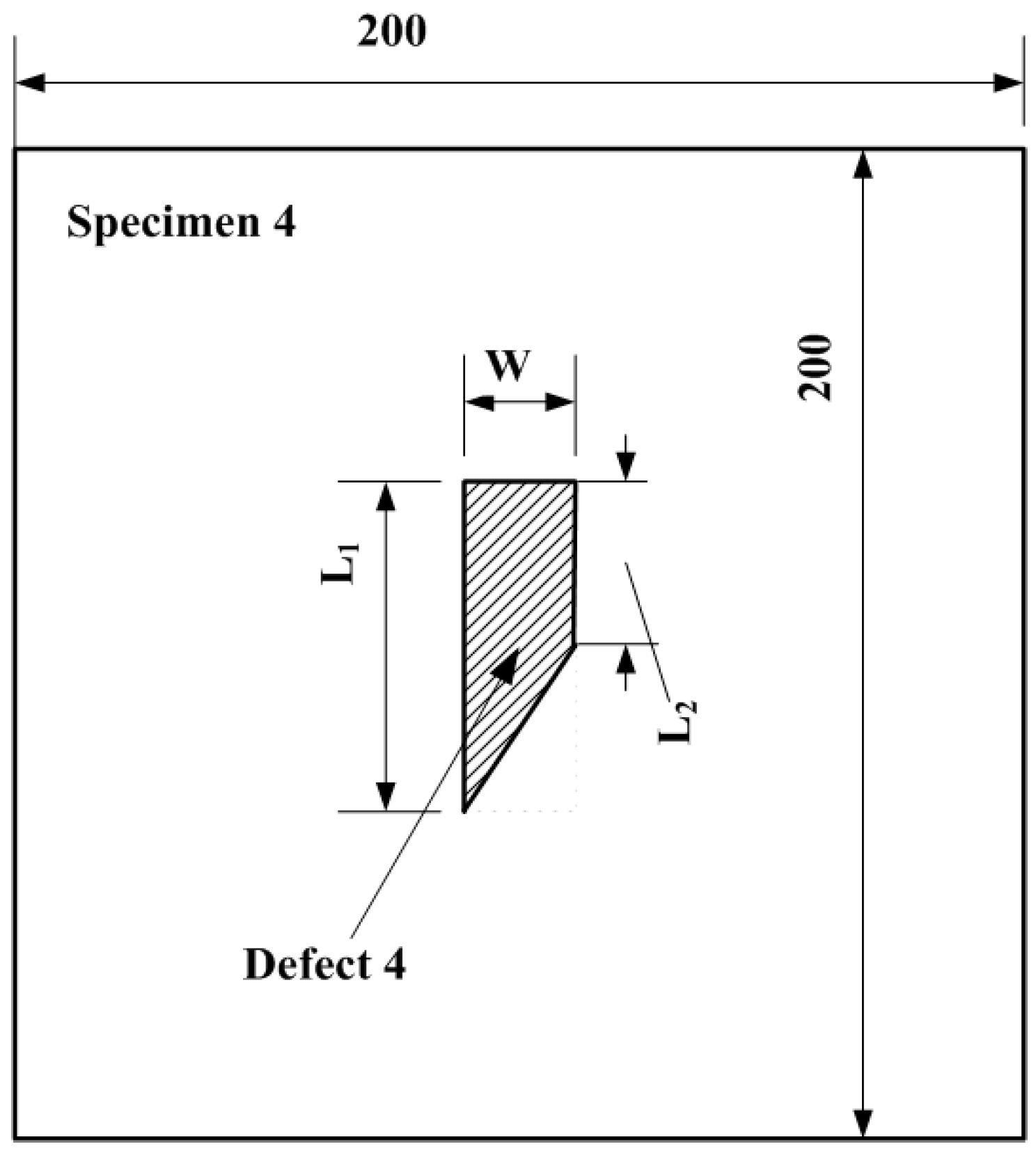
Figure 3.
A-scan response and its features.
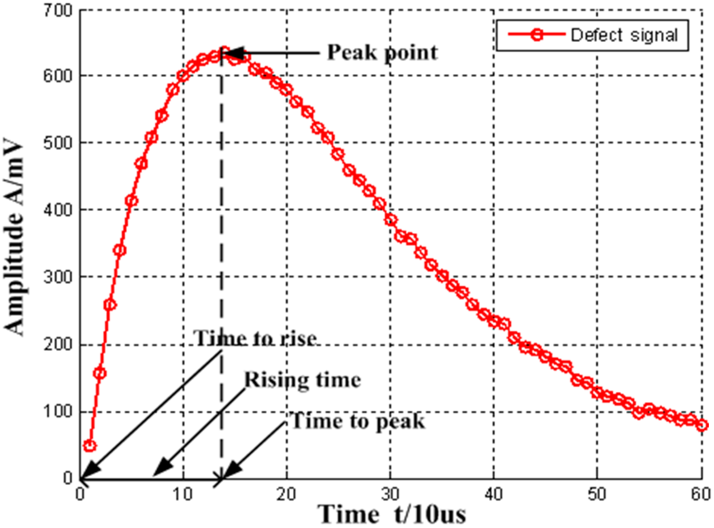
Figure 4.
Curves of the A-scan’s peak on the defect’s two sides in the direction of magnetic flux.
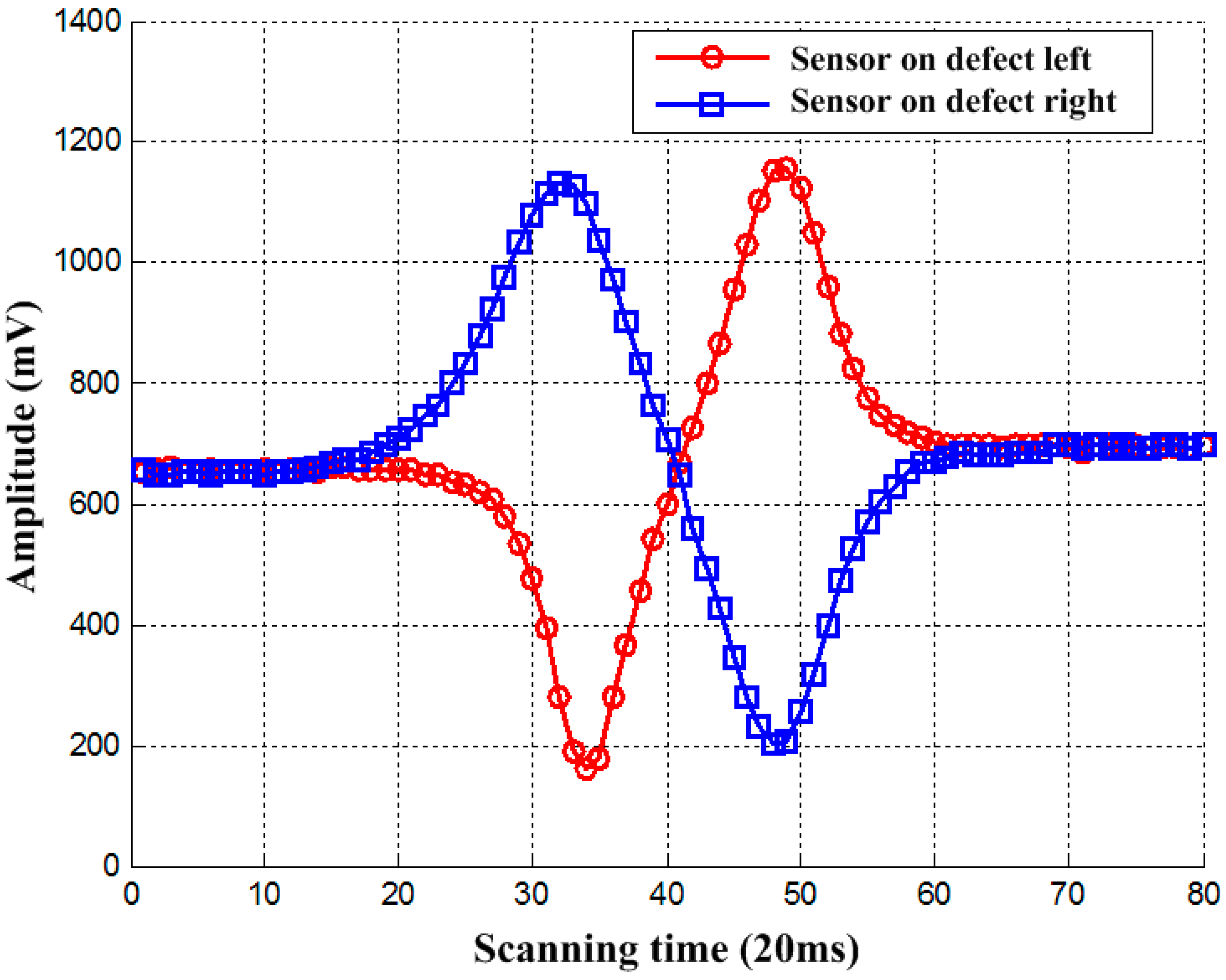
Figure 5.
Curves of the A-scan’s peak on the defect’s two sides in the direction of the current.

Figure 6.
The original C-scan contour images of defect 1.
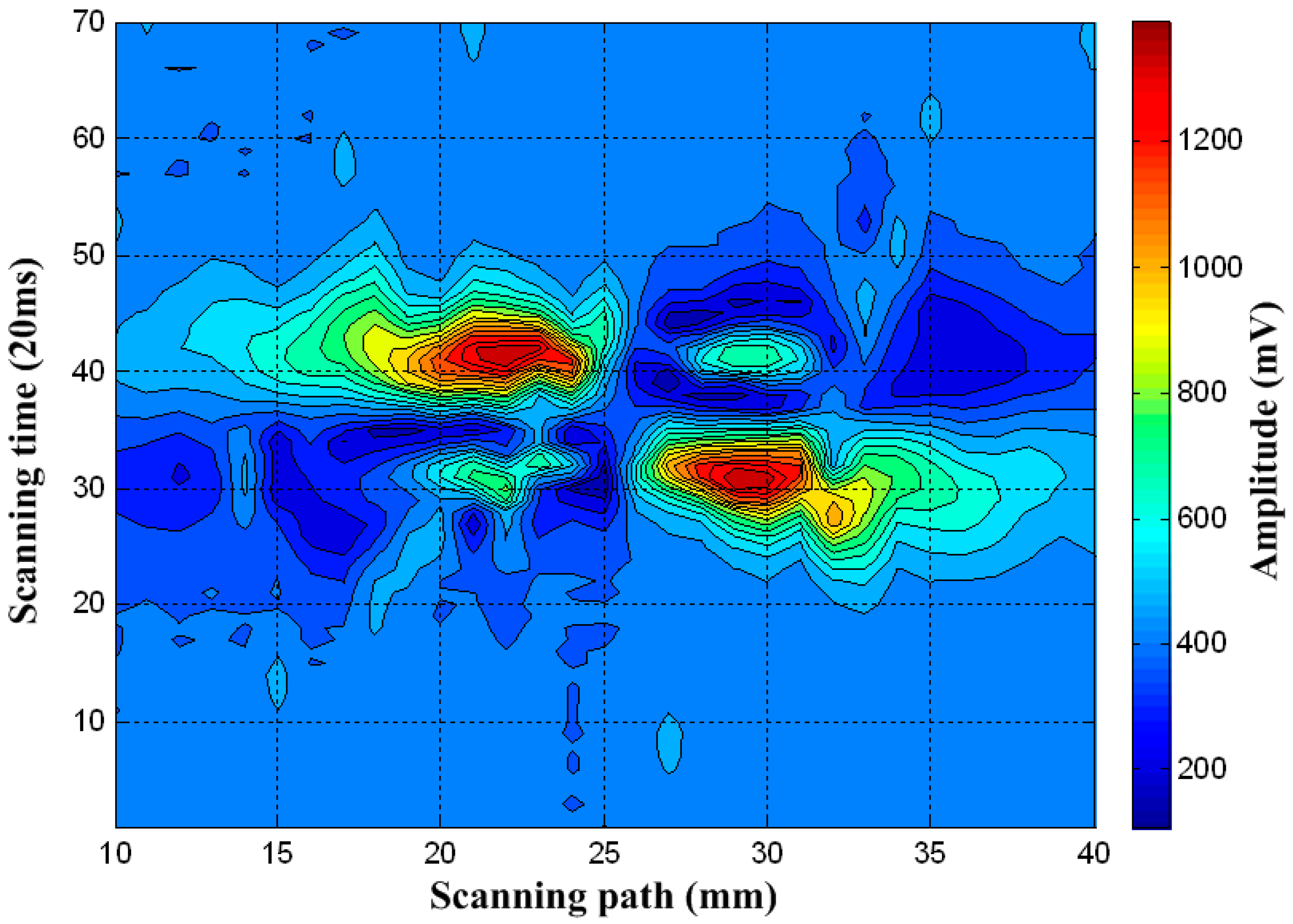
Figure 7.
C-scan images of defect 1 after a two-dimensional filter.
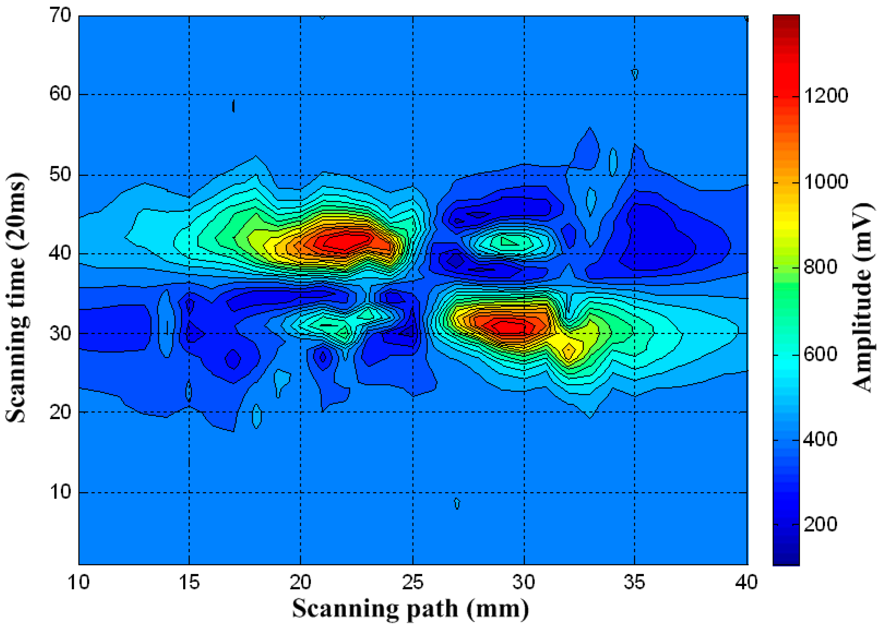
Figure 8.
C-scan outline images of defect 1 in the direction of magnetic flux.

Figure 9.
C-scan outline images of defect 2 in the direction of magnetic flux.
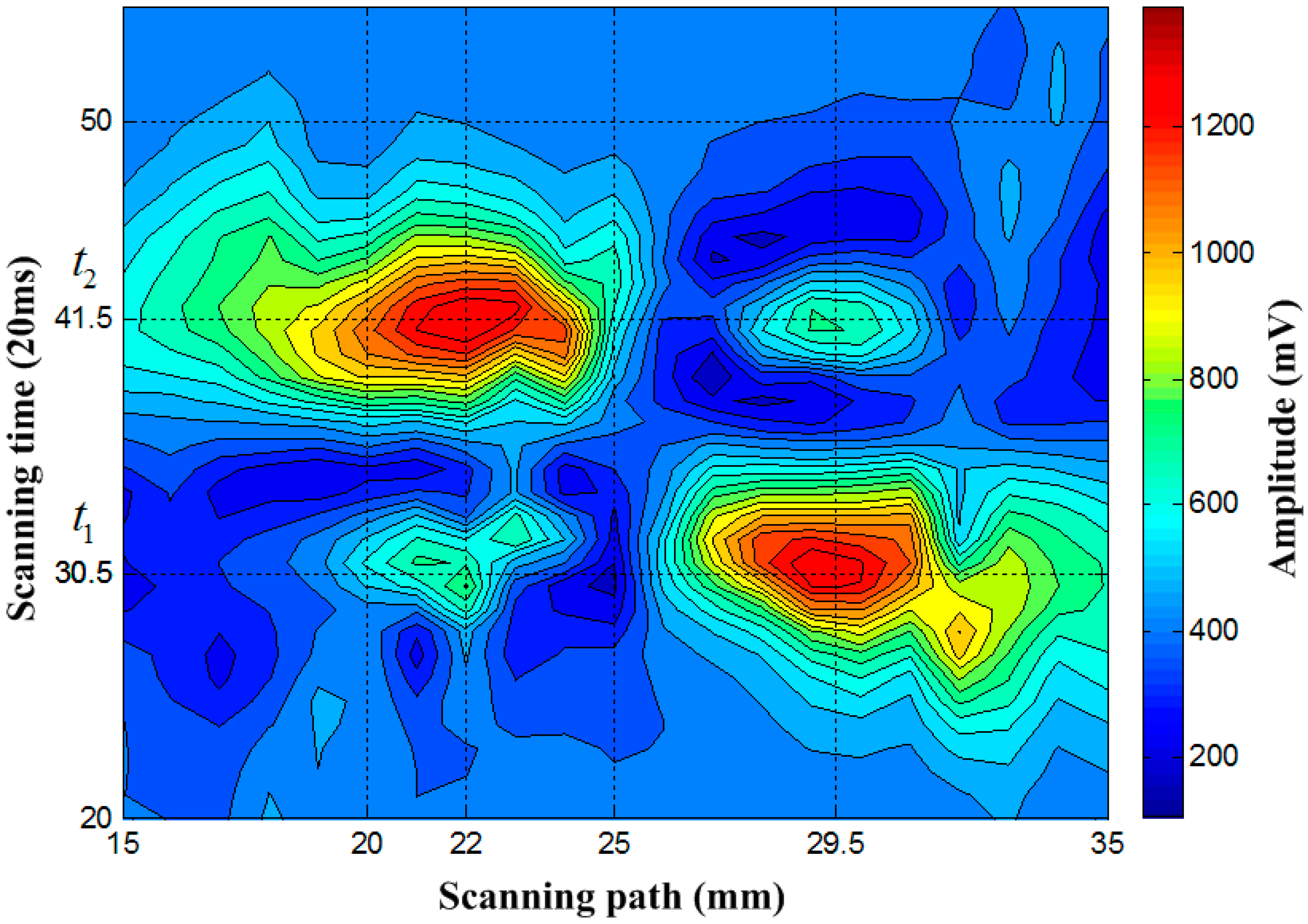
Figure 10.
C-scan outline images of defect 3 in the direction of magnetic flux.

Figure 11.
C-scan outline images of defect 1 in the direction of the exciting current.

Figure 12.
C-scan outline images of defect 2 in the direction of the exciting current.
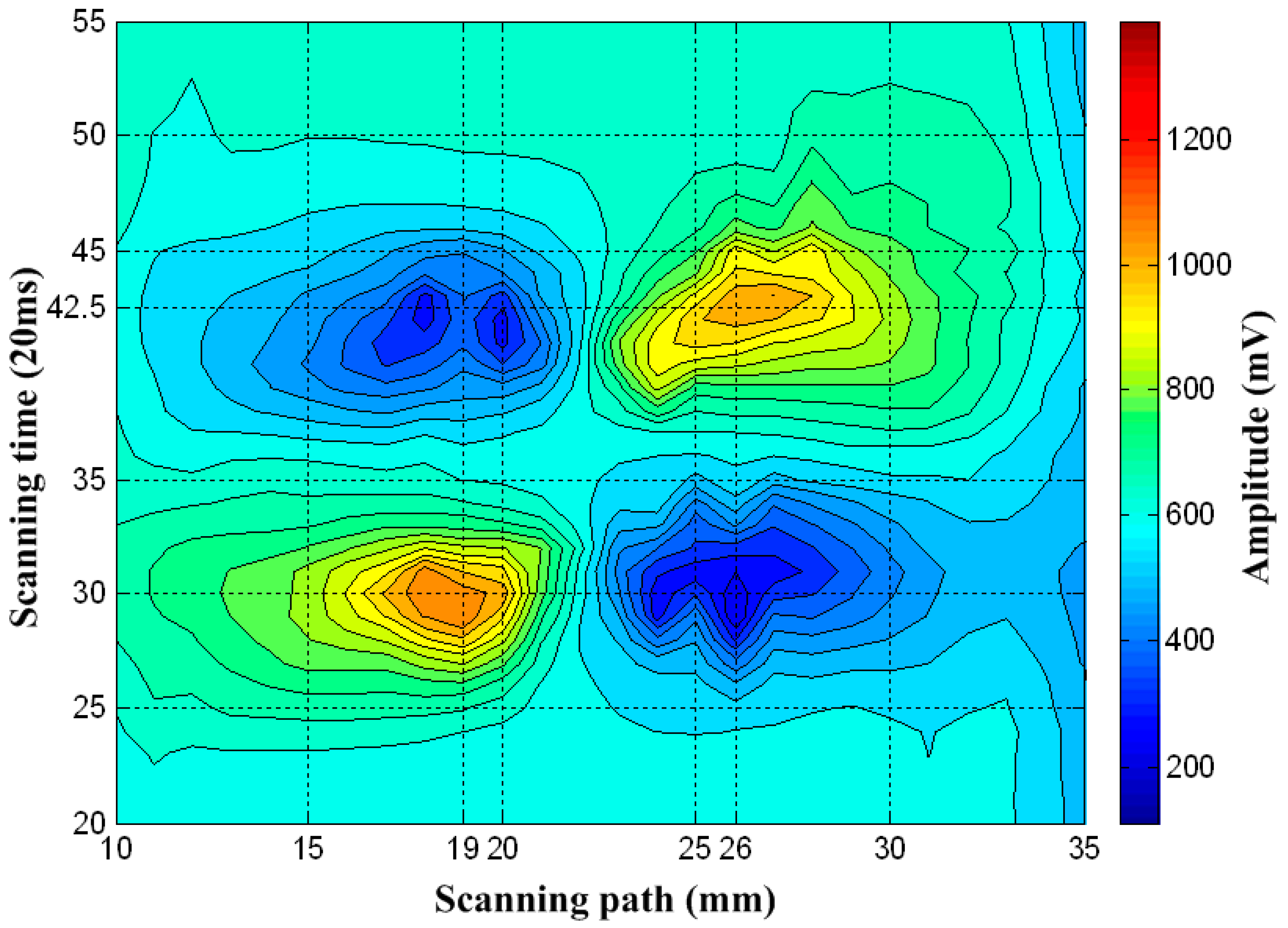
Figure 13.
C-scan outline images of defect 3 in the direction of the exciting current.

Figure 14.
C-scan contour images of subsurface defect 1.
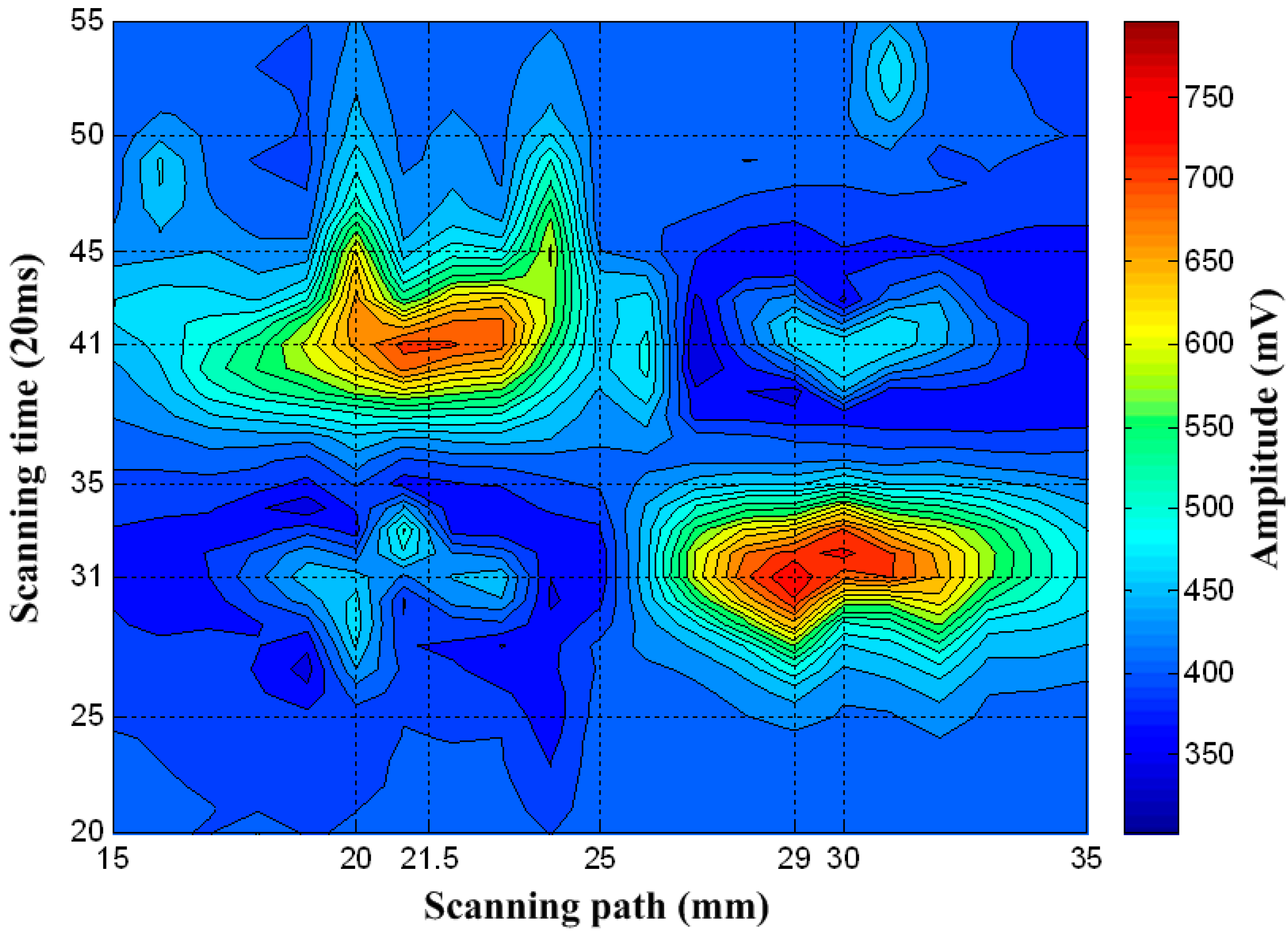
Figure 15.
C-scan contour images of irregular defect 4.

Table 1.
Parameters of the excitation coil and By pickup coil.
| Parameters | Excitation Coil | By PickUp Coil |
|---|---|---|
| Wire diameter (mm) | 0.2 | 0.05 |
| No. of turns | 400 | 600 |
| DC Resistance (ohm) | 40.2 | 39.2 |
| Inductance (mH) | 7.75 | 0.42 |
Table 2.
Estimated length and width.
| Direction | Item | Defect 1 | Defect 2 | Defect 3 |
|---|---|---|---|---|
| Magnetic induction flux | Time difference (ms) | 220 | 260 | 260 |
| Length (mm) | 13.2 | 15.6 | 15.6 | |
| Width (mm) | 7.5 | 6.5 | 5 | |
| Exciting current | Time difference (ms) | 250 | 250 | 290 |
| Length (mm) | 15 | 15 | 17.4 | |
| Width (mm) | 7 | 5.5 | 4.5 |
Table 3.
Amplitude of surface defects in two directions.
| Scanning Direction | Defect No. | Defect 1 | Defect 2 | Defect 3 |
|---|---|---|---|---|
| Magnetic induction flux | Max. amplitude (mV) | 1337.5 | 1301.1 | 1156.7 |
| Min. amplitude (mV) | 180.7149 | 194.8317 | 151.1605 | |
| Exciting current | Max. amplitude (mV) | 1089.8 | 738.4175 | 783.0181 |
| Min. amplitude (mV) | 227.4575 | 483.8115 | 654.0376 |
© 2018 by the authors. Licensee MDPI, Basel, Switzerland. This article is an open access article distributed under the terms and conditions of the Creative Commons Attribution (CC BY) license (http://creativecommons.org/licenses/by/4.0/).
Share and Cite
MDPI and ACS Style
Zhang, K.; Dong, Z.; Yu, Z.; He, Y. Shape Mapping Detection of Electric Vehicle Alloy Defects Based on Pulsed Eddy Current Rectangular Sensors. Appl. Sci. 2018, 8, 2066. https://doi.org/10.3390/app8112066
AMA Style
Zhang K, Dong Z, Yu Z, He Y. Shape Mapping Detection of Electric Vehicle Alloy Defects Based on Pulsed Eddy Current Rectangular Sensors. Applied Sciences. 2018; 8(11):2066. https://doi.org/10.3390/app8112066
Chicago/Turabian StyleZhang, Kai, Zhurong Dong, Zhan Yu, and Yunze He. 2018. "Shape Mapping Detection of Electric Vehicle Alloy Defects Based on Pulsed Eddy Current Rectangular Sensors" Applied Sciences 8, no. 11: 2066. https://doi.org/10.3390/app8112066
Note that from the first issue of 2016, this journal uses article numbers instead of page numbers. See further details here.