Effect of Substrates on the Dynamic Properties of Inkjet-Printed Ag Thin Films


Department of Mechanical Engineering, Hanyang University, 222 Wangsimni-ro, Seongdong-gu, Seoul 04763, Korea
*
Author to whom correspondence should be addressed.
†
These two authors contributed equally to this work.
Appl. Sci. 2018, 8(2), 195; https://doi.org/10.3390/app8020195
Submission received: 15 December 2017
/
Revised: 20 January 2018
/
Accepted: 25 January 2018
/
Published: 29 January 2018
(This article belongs to the Special Issue Printed Electronics 2017)
Abstract
:The dynamic properties of inkjet-printed Ag thin films on flexible substrates were measured using flexural wave propagation. The Ag nanoparticle suspension was inkjet-printed on polyimide (PI), silicon wafer, and glass. The effects of flexible substrates on the dynamic properties of the films were investigated. Beam-shaped Ag-printed substrates were fabricated by pico-second laser pulse cutting. The wave approach was presented to analyze the vibrations of the thin film on the substrates. The Young’s modulus and loss factor of the Ag thin films with the substrates were represented by the combined bending stiffness of the bilayer beam. The vibration response of the base-excited cantilever was measured using an accelerometer and laser Doppler vibrometer (LDV). Vibration transfers were analyzed to obtain dynamic characteristics of the Ag-printed bilayer beam. The substrate affects the reduction of the Ag thin film thickness during the sintering process and surface roughness of the film. The proposed method based on the wave approach allows measurement of the dynamic properties regardless of the ratio of the modulus between the thin film and substrate.
1. Introduction
With the interest in alternatives to traditional photolithography, inkjet printing has attracted considerable attention in various printed electronics applications such as flexible displays, electronic skins, flexible solar cells, and thin-film transistors [1,2,3,4,5,6]. Inkjet printing has the advantages of lowering material waste, manufacturing cost, and manufacturing process steps due to the integrated circuit pattern fabrication in flexible electronics. Moreover, inkjet technologies allow printing of precise amounts of various materials with electrical, optical, and chemical functionalities [7,8]. In addition, high precision, stability, user customization, and rapid production have encouraged the technology to expand into new applications such as patch antenna emitters, bio-sensing, biomimetic devices for providing water, and vibrational energy harvesting [9,10,11,12].
Electric circuits are produced through printing and sintering processes of liquid ink droplets on a substrate. The densification and electrical performance are affected by various factors during sintering. Proper sintering conditions allow the design of printed devices for high performance. In previous studies, temperature was the major factor, which improved the quality of the film and determined the complete densification process [13,14]. Pressure was used to reduce the temperatures required to improve the conductivities during the sintering process [15]. The thickness of the film increased in proportion to the number of overprints. It was determined that the Young’s modulus and the hardness of the film are dependent on the film thickness [16,17]. The electrical performance of thin film transistors was optimized by adjusting the thickness of the film [18]. The electrical resistivity and physical deformations of the film after sintering were also related to the substrate [19,20].
Since mechanical properties directly affect the performance of flexible electronic products, the Young’s modulus and loss factor of the thin film should be identified to make highly reliable products. The nanoindentation test was developed to measure the properties of thin films. [21,22]. When the indenter is pressed into the specimen, the Young’s modulus is obtained from the load–displacement curves. This method using an indenter causes damage to the specimen due to plastic deformations [23]. The accuracy of the measurement is not guaranteed for hard films on soft substrates [14].
Modal analysis is a common method to measure the dynamic properties of a beam. The cantilever beam is widely used for measuring due to the clear implementation of boundary conditions associated with accuracy [24,25]. Methods based on modal properties utilize the resonance frequencies of the vibrating system. The measured resonance frequencies generally encounter assorted unwanted conditions such as noise and nonlinear responses. These aspects require complicated signal processing to accurately measure the properties of the beams.
In this study, flexural wave propagation was utilized to estimate the dynamic characteristics of inkjet-printed Ag thin films. The surface morphology of the inkjet-printed Ag thin film was measured using a 3D optical profiler. Experiments were conducted with the inkjet-printed Ag thin film on varied substrates. The effects of the substrate on the dynamic properties of the film were investigated. The wave approach was presented to analyze vibrations of the thin film on the substrates. The Young’s modulus and loss factor of Ag thin films with the substrates were represented by the combined bending stiffness of the bilayer beam. Vibration transfer on the bilayer beams was measured. The dynamic properties of the thin film were obtained numerically using the vibration transfer with regard to the properties of the substrates. The proposed method allows the dynamic properties of the thin film on arbitrary substrates to be determined. The inkjet-printed Ag thin films were evaluated through vibration transfer without plastic deformation of the specimens.
2. Vibration Transfer of Ag Inkjet-Printed on Flexural Substrates
2.1. Flexural Wave Propagation of Inkjet-Printed Substrates
The effects of shear deformation and rotary inertia are negligibly small compared to those of the bending deformation due to the small thickness and width of the substrates. The equation of motion for inkjet-printed substrates excited in the transverse direction is expressed as [26]
where is the bending stiffness, is the deflection, is the lengthwise coordinate from the origin, and is the mass per unit length of the beam. Assuming the harmonic vibration is given by , the vibration response of a substrate is obtained from the following equation:
where are complex coefficients, is the length of the beam, and is the complex wavenumber. To consider the vibration dissipation of wave propagation, the complex stiffness was used as , where is the loss factor. Substituting Equation (1) into (2), the complex wavenumber is derived as
To solve the unknown coefficients, , the boundary conditions are applied as
The transfer function between the vibration responses at and the input excitation, , is calculated as follows:
where and are the amplitude and phase of the transfer function, respectively.
The complex wavenumbers, , were calculated numerically using the measured transfer function [27]. The iteration matrix equation of the Newton–Rapson method is given as
The complex bending stiffness with frequency was obtained using the calculated wavenumber.
2.2. Bending Stiffness of the Bilayer Beams for Analyzing Vibrations on the Inkjet-Printed Ag Thin Films
To analyze the vibration transfer of ink on the substrates, the combined bending stiffness of the bilayer beam was used. The bilayer beam consists of the substrate and the printed ink. To obtain the Young’s modulus of the film on the substrate, the bending stiffness of the substrate should be identified. When the strain distribution is linear across the thickness of the bilayer beam, the stress equilibrium for the neutral axis is expressed as [28]
where and are the thicknesses of the substrate and the film, respectively, is the distance of neutral axis from the surface of the beam, and are the Young’s moduli of the substrate and the film, respectively, and is the thickness-wise coordinate from the neutral axis. The distance, , is determined from Equation (7) as
The moment equilibrium about the neutral axis is given as [29]
After substituting Equation (8) into Equation (9) and integrating Equation (9), the combined complex bending stiffness for the internal damping effect of the beam is derived as
The thicknesses of the substrate and the film were measured. The Young’s moduli of the substrate without and with the film were calculated in the anterior procedure. To obtain the Young’s modulus of the film, , the known values were substituted into Equation (10), which is a function of the Young’s modulus of the film.
3. Measuring the Dynamic Properties of Ag Ink on Flexural Substrates
3.1. Specimen Fabrication and Experimental Setup
The substrates used for the experiments were two polyimide (PI) films (SKC, Seoul, Korea) with thicknesses of 25 μm and 225 μm, slide glass with a thickness of 145 μm, and a silicon wafer (LG Siltron Inc., Gumi, Korea) with a thickness of 200 μm. To remove surface contamination, the substrates were first ultrasonicated in isopropyl alcohol (Daejung chemicals & metals, Siheung, Korea) for 20 min and rinsed with a deionized water for 10 min. For proper wettability of the substrates, C4F8 gas (99.99%) (Daesung industrial gases Co., Seoul, Korea) was used. The substrates were treated in O2 and Ar plasmas to remove any remaining contamination from organic matter. A MicroFab piezoelectric print head (MicroFab Co., Plano, TX, USA) with a 30 μm nozzle diameter was used to perform inkjet printing on the plasma-treated surface.
The Ag ink used in this study was a silver nanoparticle colloid in tetradecane (Harima Chemical Co., Tokyo, Japan). The ink contained 57.3 wt % silver nanoparticles with diameters below 10 nm. The viscosity of the Ag ink was 8.4 mPa·s at 20 °C. The applied voltage was controlled to ensure accuracy of the droplet generator (MicroFab Co., Plano, TX, USA). The printing resolution was adjusted to 800 dpi, and the drop diameter was set to 30 μm. Due to the controlled conditions, the average diameter of a single droplet on the substrate was maintained at 55 μm.
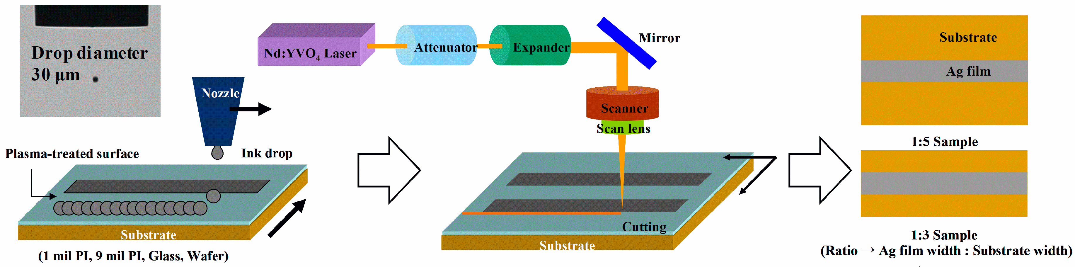
The Ag thin films on the substrates were printed as shown in Figure 1. To satisfy the performance of conductivity and mechanical properties, the inkjet-printed thin films were sintered at 210 °C for one hour. The width and thickness of the film were designed to be 100 μm and 1.5 μm, respectively, when the number of overprints was one. The actual printed width and thickness had variations affected by the properties of the substrates. To conduct the vibration test, the beam shape specimens were obtained by Nd:YVO4 laser pulse cutting (with a 10 ps pulse width, a 343 nm wavelength, and a 400 kHz frequency). The printed specimens had different widths depending on the substrate: the PI and glass had widths of 500 μm, and the silicon wafer had a width of 300 μm.
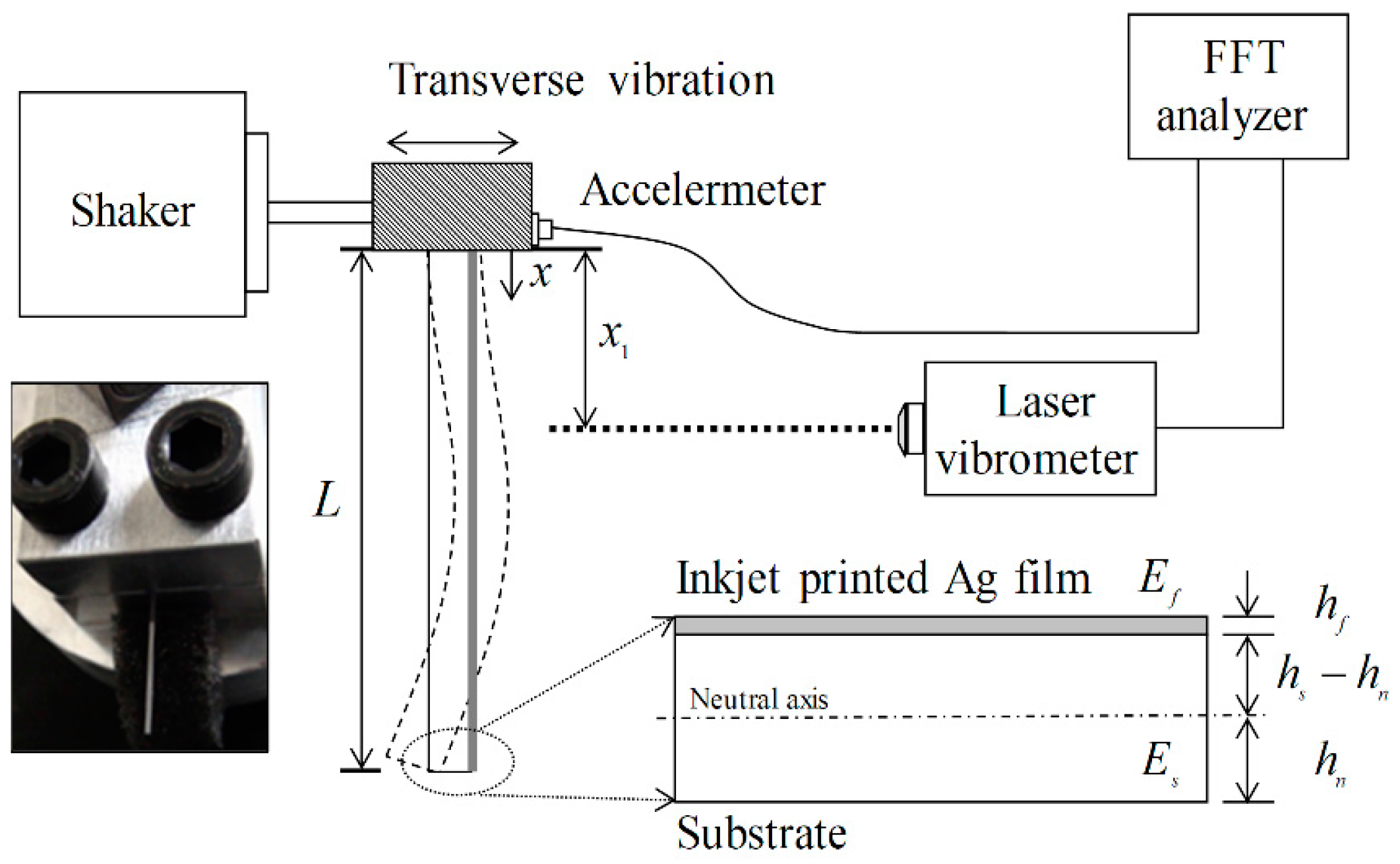
Figure 2 shows the experimental set-up with the printed bilayer beams. Transverse vibrations were excited on the beams by the vibration shaker. The vibration responses were measured with a laser Doppler vibrometer (LDV) (OFV-503, Polytec, Hörsching, Austria) and an accelerometer (2250A -10, Endevco, Irvine, CA, USA). The two sensors were calibrated by measurement of the vibration response on the same point, with the clamped end of the beam excited with random noise. The location of the LDV was adjusted at to obtain the vibration response of the beam. The transfer functions of the bare substrate and Ag-printed beam were measured to estimate the properties of the Ag films.
3.2. Morphology and Characteristics of Ag Films
To calculate the average thickness, the morphology of inkjet-printed thin films was measured using a 3D optical profiler (Nano View NV-P2020, NanoSystem, Daejeon, Korea). The degree of densification during the sintering process determines the Young’s modulus of the ink. With an identical overprint number and sintering process, densification by grain growth induces thickness reduction [16]. Figure 3 shows typical surface images and profiles on the PI, silicon wafer, and glass substrates. The mean value calculated by surface profiles at five locations was utilized as a representative thickness of the Ag film printed on each beam. The sintering process changes the rectangular cross-sectional shape into a rough semi-circular shape due to central collapse during densification [30]. The silver formation, i.e., the grain size, the surface roughness, and the thickness of the Ag film, is affected by the sintering temperature and the number of overprints [16]. As the high sintering temperature helped reduce the film thickness, the grain growth depended on the substrate. The thickness of the Ag film decreased with a soft surface during the sintering process. The bending stiffness was proportional to the third power of thickness, but the rough surface was not included in the thickness. When the Ag film became thinner, densification was greater under the same sintering conditions.
The 3D optical profiles indicated substrate influence on the surface roughness and thickness of the Ag film. The thin films on the PI had a larger thickness than those on the silicon wafer and the glass. The average thickness and standard deviation at five locations on the PI, silicon wafer, and glass were 1.91 ± 0.11 μm, 1.85 ± 0.05 μm, and 1.53 ± 0.04 μm, respectively.
3.3. Dynamic Properties of the Ag Films
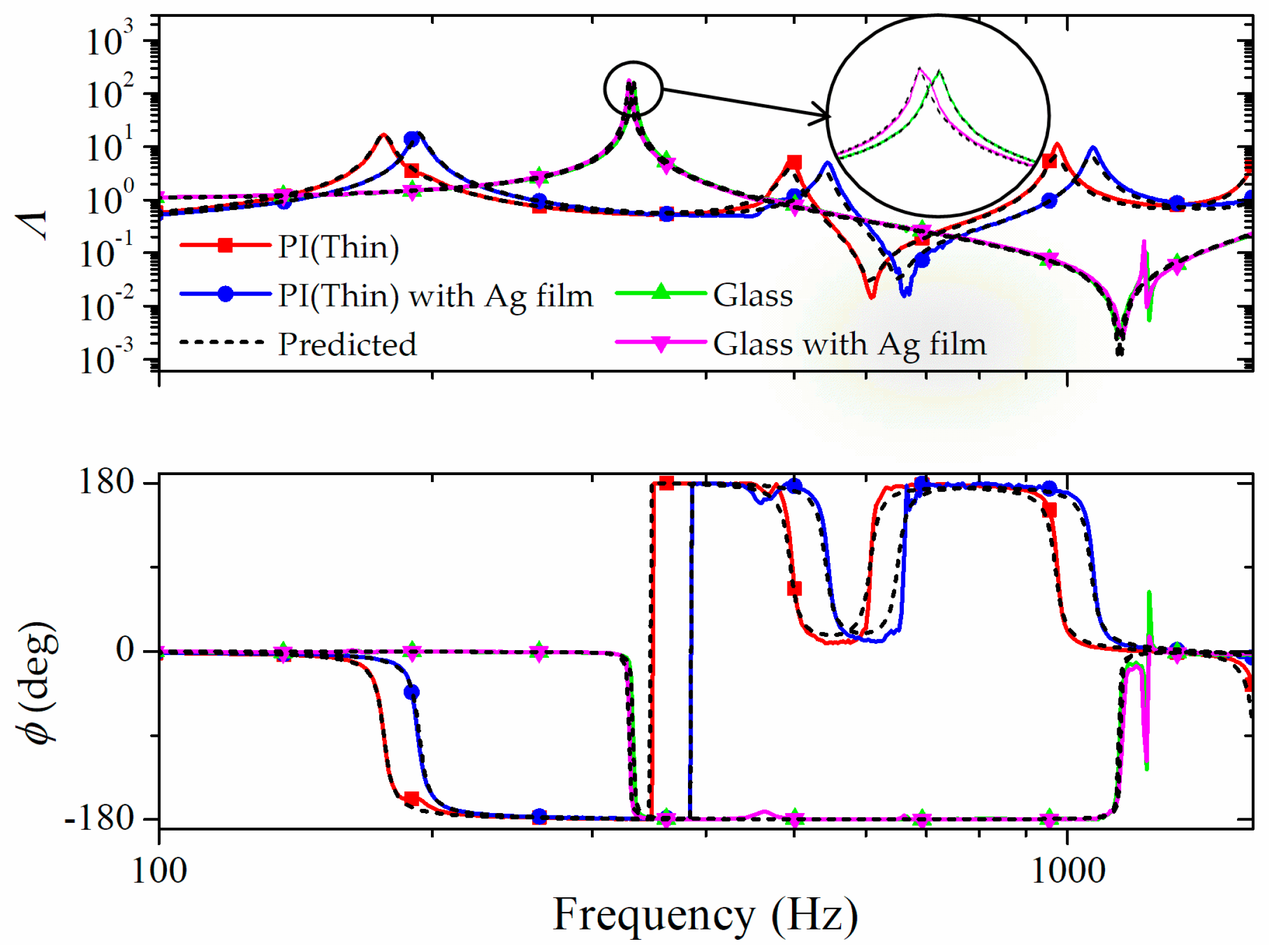
The wave propagations on the beam are dependent on the bending stiffness and mass per unit length of the beam. The combined bending stiffness was obtained from Equation (10). The mass per unit length of the bilayer was calculated as the simple sum of the values. Figure 4 shows the measured transfer functions of the bare substrates and the Ag-printed PI and glass beams. The predicted functions were plotted using the derived properties in Figure 5. The vibration transfers in Figure 4 showed evident variations due to the printing process. The vibration responses of PI shifted higher, and those of the silicon wafer and glass shifted to lower frequencies. The effects of Ag ink were determined by the stiffness and mass per length of the substrates. These variations definitely show that the properties of the Ag ink were correlated with the substrates.
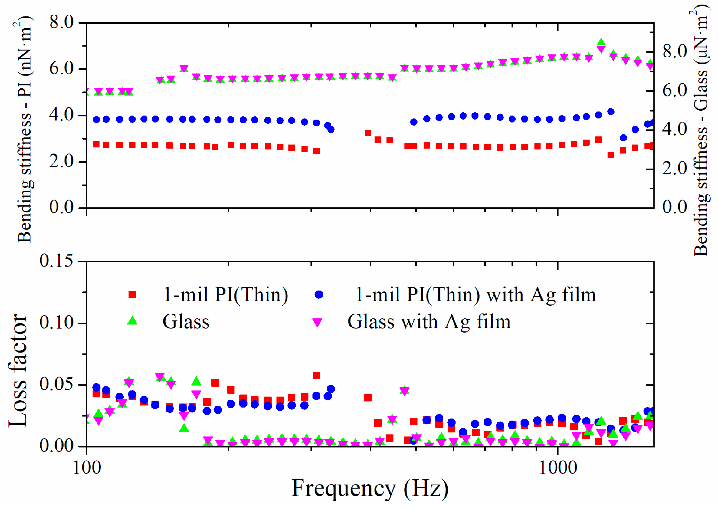
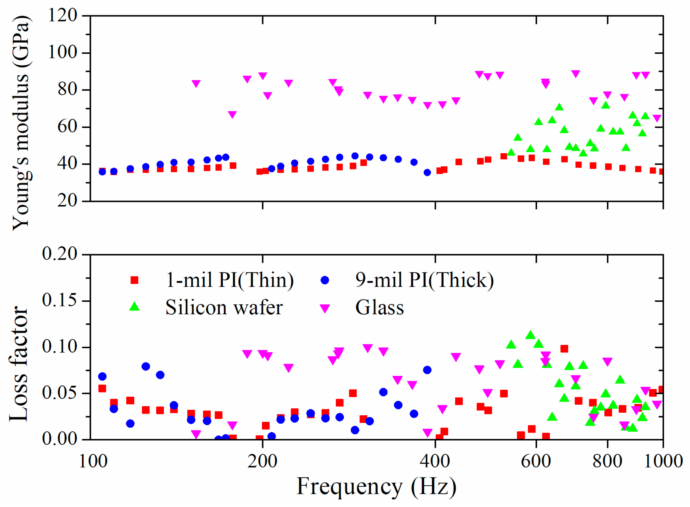
Figure 5 shows the bending stiffness and loss factor of the bare substrates and the bilayer beams. The obtained properties were calculated numerically through Equations (3) and (6). The averaged properties were used as representative values to minimize errors. The Young’s modulus and loss factor of the inkjet-printed Ag thin films were calculated by solving Equation (10). The results of the numerical calculation were shown in Figure 6. The acquired Young’s modulus of the Ag thin films on the thin PI, the thick PI, the silicon wafer, and the glass were 38.5 GPa, 41.1 GPa, 55.2 GPa, and 75.4 GPa, respectively, and the acquired loss factors were 0.03, 0.036, 0.047, and 0.058, respectively. Even though the same ink was used, the Young’s modulus of the ink, depending on the substrate, varied considerably. The loss factor tended to increase with increments of the modulus. Based on the measured properties of the thin PI and the thick PI, the modulus and loss factor depended on the type of substrate when the sintering process was identical. These trends suggest that the effect of the substrate should be considered to obtain the mechanical properties of the ink.
The densification of the Ag film depends on the substrate due to differences in the coefficient of thermal expansion [19]. Densification is known to be affected by temperature, pressure, the number of overprints, and grain size [14,15]. As densification reaches completion, the Young’s modulus of the Ag film converges to that of silver. When nanoparticles of silver ink are formed during the sintering process, the geometric properties change. The surface roughness and thickness fluctuations may cause a systematic error in the measuring method. The wave approach allows accurate measuring of the properties because wave propagation on the printed substrates considers physical changes directly. In this study, the dynamic properties were obtained numerically as discussed earlier using the wave approach. The Young’s modulus and loss factor were directly determined without any damage to the thin film due to the wave approach.
4. Conclusions
The proposed method based on the wave approach was introduced to measure the Young’s modulus and loss factor of inkjet-printed Ag thin films on various substrates. The effect of the substrate on the properties of the printed films was discussed with respect to the morphology of the film. The vibration transfers of the printed film were compared according to substrate. Alterations of the vibration responses due to the printing process showed different tendencies. The vibration transfers on the inkjet-printed substrates were analyzed using the bilayer beam. The bending stiffness and loss factor of the printed beam were obtained numerically. Through the proposed method, the Young’s modulus and loss factor of the ink were determined for various substrates. The dynamic properties of the ink varied considerably according to the substrates. When the thickness of the Ag film decreased under the identical sintering condition, the Young’s modulus and the loss factor increased. The Young’s moduli of the Ag films on the substrates were measured to be 46.4–90.8% of that of silver. The loss factor tended to increase with the increment of the modulus. The proposed method reliably determines the dynamic properties of the thin film regardless of the substrate characteristics. The Young’s modulus and loss factor were directly determined using the vibration response on the bare substrate and the bilayer without any damage to the thin film. It is also applicable to large structures since the proposed methodology utilizes vibration modal properties. The vibration modal properties are fundamental characteristics and appear for structures of arbitrary geometry. With the rapid advances in printed electronics and 3D printing technologies, the materials used for the construction includes a wide variety of components. For reliability testing or performance evaluations, knowledge of the dynamic material properties is crucial for studying the influence of each components on the whole dynamic behavior. The proposed method allows the rapid laboratory determination of dynamic properties with small vibration measurements and is beneficial when many components need to be characterized.
Acknowledgments
This research was supported by a Grant (17RTRP-B072484-05) from the Railroad Technology Research Program funded by the Ministry of Land, Infrastructure and Transport of the Korean government.
Author Contributions
Deokman Kim and Yunsang Kwak developed the theoretical model, analyzed the data, and performed the experiments; Junhong Park conceived and supervised the research project; all of the authors contributed to the writing.
Conflicts of Interest
The authors declare no conflict of interest.
References
- Kang, B.J.; Oh, J.H. Geometrical characterization of inkjet-printed conductive lines of nanosilver suspensions on a polymer substrate. Thin Solid Films 2010, 518, 2890–2896. [Google Scholar] [CrossRef]
- Wei, Z.; Chen, H.; Yan, K.; Yang, S. Inkjet printing and instant chemical transformation of a CH3NH3PbI3/Nanocarbon electrode and interface for planar perovskite solar cells. Angew. Chem. 2014, 126, 13455–13459. [Google Scholar] [CrossRef]
- Oh, J.H.; Lim, S.Y. Precise size control of inkjet-printed droplets on a flexible polymer substrate using plasma surface treatment. J. Micromech. Microeng. 2009, 20, 015030. [Google Scholar] [CrossRef]
- Wood, V.; Panzer, M.J.; Chen, J.; Bradley, M.S.; Halpert, J.E.; Bawendi, M.G.; Bulović, V. Inkjet-printed quantum dot–polymer composites for full-color AC-driven displays. Adv. Mater. 2009, 21, 2151–2155. [Google Scholar] [CrossRef]
- Graddage, N.; Chu, T.-Y.; Ding, H.; Py, C.; Dadvand, A.; Tao, Y. Inkjet printed thin and uniform dielectrics for capacitors and organic thin film transistors enabled by the coffee ring effect. Org. Electron. 2016, 29, 114–119. [Google Scholar] [CrossRef]
- Benight, S.J.; Wang, C.; Tok, J.B.; Bao, Z. Stretchable and self-healing polymers and devices for electronic skin. Prog. Polym. Sci. 2013, 38, 1961–1977. [Google Scholar] [CrossRef]
- Bai, J.G.; Creehan, K.D.; Kuhn, H.A. Inkjet printable nanosilver suspensions for enhanced sintering quality in rapid manufacturing. Nanotechnology 2007, 18, 185701. [Google Scholar] [CrossRef]
- Dong, H.; Carr, W.W.; Morris, J.F. An experimental study of drop-on-demand drop formation. Phys. Fluids 2006, 18, 072102. [Google Scholar] [CrossRef]
- Agarwala, S.; Yeong, W.Y. 3D printed electronic tracks for bio-integrated free-form devices. In Proceedings of the 2nd International Conference on Progress in Additive Manufacturing, Singapore, 16–19 May 2016. [Google Scholar]
- Zhang, L.; Wu, J.; Hedhili, M.N.; Yang, X.; Wang, P. Inkjet printing for direct micropatterning of a superhydrophobic surface: Toward biomimetic fog harvesting surfaces. J. Mater. Chem. A 2015, 3, 2844–2852. [Google Scholar] [CrossRef]
- Goh, G.L.; Ma, J.; Chua, K.L.F.; Shweta, A.; Yeong, W.Y.; Zhang, Y.P. Inkjet-printed patch antenna emitter for wireless communication application. Virtual Phys. Prototyp. 2016, 11, 289–294. [Google Scholar] [CrossRef]
- Andò, B.; Baglio, S.; Bulsara, A.R.; Marletta, V.; Ferrari, V.; Ferrari, M. A low-cost snap-through-buckling inkjet-printed device for vibrational energy harvesting. IEEE Sens. J. 2015, 15, 3209–3220. [Google Scholar] [CrossRef]
- Zhu, Q.; Fan, B. Low temperature sintering of 8YSZ electrolyte film for intermediate temperature solid oxide fuel cells. Solid State Ionics 2005, 176, 889–894. [Google Scholar] [CrossRef]
- Lee, D.J.; Oh, J.H. Inkjet printing of conductive Ag lines and their electrical and mechanical characterization. Thin Solid Films 2010, 518, 6352–6356. [Google Scholar] [CrossRef]
- Albert, A.D.; Becker, M.F.; Keto, J.W.; Kovar, D. Low temperature, pressure-assisted sintering of nanoparticulate silver films. Acta Mater. 2008, 56, 1820–1829. [Google Scholar] [CrossRef]
- Park, J.; Lee, D.J.; Kim, S.J.; Oh, J.H. Dynamic characteristics measurements of inkjet-printed thin films of nanosilver suspensions on a flexible plastic substrate. J. Micromech. Microeng. 2009, 19, 095021. [Google Scholar] [CrossRef]
- Greer, J.R.; Street, R.A. Mechanical characterization of solution-derived nanoparticle silver ink thin films. J. Appl. Phys. 2007, 101, 103529. [Google Scholar] [CrossRef]
- Wang, Y.; Sun, X.W.; Goh, G.K.L.; Demir, H.V.; Yu, H.Y. Influence of channel layer thickness on the electrical performances of inkjet-printed In-Ga-Zn oxide thin-film transistors. IEEE Trans. Electron Devices 2011, 58, 480–485. [Google Scholar] [CrossRef] [Green Version]
- Lee, D.J.; Oh, J.H.; Bae, H.S. Crack formation and substrate effects on electrical resistivity of inkjet-printed Ag lines. Mater. Lett. 2010, 64, 1069–1072. [Google Scholar] [CrossRef]
- Wang, W.-K.; Huang, S.-Y.; Jiang, M.-C.; Wuu, D.-S. Optoelectronic properties and structural characterization of GaN thick films on different substrates through pulsed laser deposition. Appl. Sci. 2017, 7, 87. [Google Scholar] [CrossRef]
- Oh, C.-S.; Lee, H.-J.; Ko, S.-G.; Kim, S.-W.; Ahn, H.-G. Comparison of the young’s modulus of polysilicon film by tensile testing and nanoindentation. Sens. Actuators A 2005, 117, 151–158. [Google Scholar] [CrossRef]
- Saha, R.; Nix, W.D. Effects of the substrate on the determination of thin film mechanical properties by nanoindentation. Acta Mater. 2002, 50, 23–38. [Google Scholar] [CrossRef]
- Li, X.; Bhushan, B. A review of nanoindentation continuous stiffness measurement technique and its applications. Mater. Charact. 2002, 48, 11–36. [Google Scholar] [CrossRef]
- Ozdoganlar, O.B.; Hansche, B.D.; Carne, T.G. Experimental modal analysis for microelectromechanical systems. Exp. Mech. 2005, 45, 498–506. [Google Scholar] [CrossRef]
- Burdess, J.S.; Harris, A.J.; Wood, D.; Pitcher, R.J.; Glennie, D. A system for the dynamic characterization of microstructures. J. Microelectromech. Syst. 1997, 6, 322–328. [Google Scholar] [CrossRef]
- Fahy, F.J. Sound and Structural Vibration: Radiation, Transmission and Response; Academic Press: Cambridge, MA, USA, 2012. [Google Scholar]
- Park, J. Transfer function methods to measure dynamic mechanical properties of complex structures. J. Sound Vib. 2005, 288, 57–79. [Google Scholar] [CrossRef]
- Hibbeler, R. Mechanics of Materials; Prentice Hall: Upper Saddle River, NJ, USA, 1997. [Google Scholar]
- Verver, M.M.; de Lange, R.; van Hoof, J.; Wismans, J.S. Aspects of seat modelling for seating comfort analysis. Appl. Ergon. 2005, 36, 33–42. [Google Scholar] [CrossRef] [PubMed]
- Park, J.-W.; Baek, S.-G. Thermal behavior of direct-printed lines of silver nanoparticles. Scr. Mater. 2006, 55, 1139–1142. [Google Scholar] [CrossRef]
Figure 1.
Schematic of the printing procedure to fabricate the test specimen using a MicroFab piezoelectric print head and Nd:YVO4 laser pulse cutting.
Figure 1.
Schematic of the printing procedure to fabricate the test specimen using a MicroFab piezoelectric print head and Nd:YVO4 laser pulse cutting.

Figure 2.
Experimental set-up to measure wave propagation on the specimen. The inset shows a cross section of the specimen bilayer structure. FFT: Fast Fourier transform.
Figure 2.
Experimental set-up to measure wave propagation on the specimen. The inset shows a cross section of the specimen bilayer structure. FFT: Fast Fourier transform.

Figure 3.
Surface morphology of inkjet-printed Ag thin films sintered on various substrates. (a) The typical surface image and (b) profiles of the substrates. PI: Polyimide.
Figure 3.
Surface morphology of inkjet-printed Ag thin films sintered on various substrates. (a) The typical surface image and (b) profiles of the substrates. PI: Polyimide.
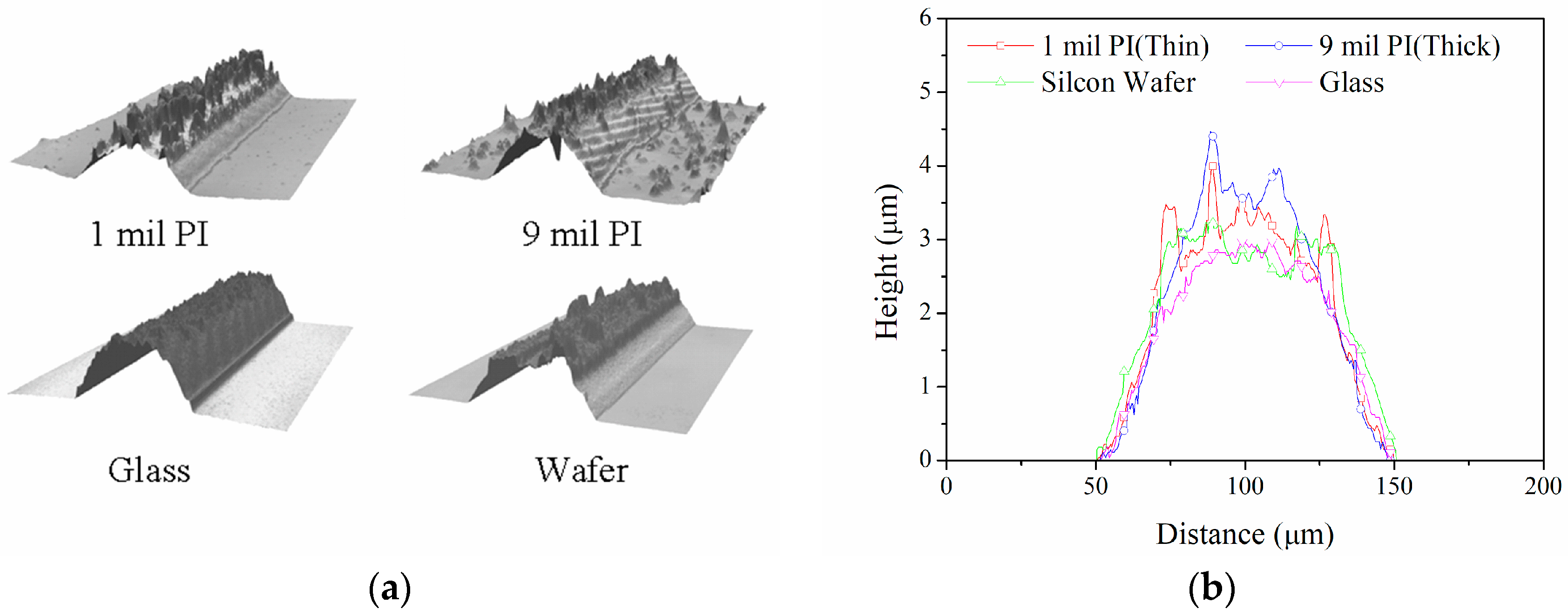
Figure 4.
Measured transfer function of Ag-printed beams on PI and glass substrates. The alterations of vibration responses due to the printing process showed different tendencies according to substrate.
Figure 4.
Measured transfer function of Ag-printed beams on PI and glass substrates. The alterations of vibration responses due to the printing process showed different tendencies according to substrate.

Figure 5.
Measured bending stiffness and loss factor of the bare substrates and the Ag-printed beams.
Figure 5.
Measured bending stiffness and loss factor of the bare substrates and the Ag-printed beams.

Figure 6.
Young’s moduli and loss factors of the inkjet-printed Ag film on various substrates. The mechanical properties of the ink varied considerably depending on the substrate. These tendencies suggest the effect of the substrate should be considered to accurately obtain the properties of the ink.

© 2018 by the authors. Licensee MDPI, Basel, Switzerland. This article is an open access article distributed under the terms and conditions of the Creative Commons Attribution (CC BY) license (http://creativecommons.org/licenses/by/4.0/).
Share and Cite
MDPI and ACS Style
Kim, D.; Kwak, Y.; Park, J. Effect of Substrates on the Dynamic Properties of Inkjet-Printed Ag Thin Films. Appl. Sci. 2018, 8, 195. https://doi.org/10.3390/app8020195
AMA Style
Kim D, Kwak Y, Park J. Effect of Substrates on the Dynamic Properties of Inkjet-Printed Ag Thin Films. Applied Sciences. 2018; 8(2):195. https://doi.org/10.3390/app8020195
Chicago/Turabian StyleKim, Deokman, Yunsang Kwak, and Junhong Park. 2018. "Effect of Substrates on the Dynamic Properties of Inkjet-Printed Ag Thin Films" Applied Sciences 8, no. 2: 195. https://doi.org/10.3390/app8020195
Note that from the first issue of 2016, this journal uses article numbers instead of page numbers. See further details here.