1. Introduction
The recent explosive growth of mobile traffic has created a demand for increased bandwidths and faster data rates in telecommunication. As a frequency band candidate for fifth-generation (5 G) communication to solve this traffic increase, not only a band below 6 GHz but also Ka-band communication, especially 28 GHz and 39 GHz, has been attracting attention. Also, for terrestrial-satellite backhaul network communication, 17.7–20.2 GHz for downlink and 27.5–30 GHz for uplink are considered in the Ka-band [
1,
2,
3]. Due to the short wavelengths corresponding to these frequency bands, compact phased-array antennas can be realized using wafer-scale, on-chip antennas or printed circuit-board antennas, as well as mm-wave, complementary metal oxide semiconductor (CMOS)-integrated circuit technology [
4,
5,
6,
7]. Many studies on the development of communication systems using multi-antenna array structures with mm-wave bands have been reported [
8,
9,
10,
11,
12]. The front-end of the phased-array transceiver is usually composed of a single-pole, double-throw (SPDT) switch, low-noise amplifier (LNA), power amplifier (PA), and phase shifters (PS).
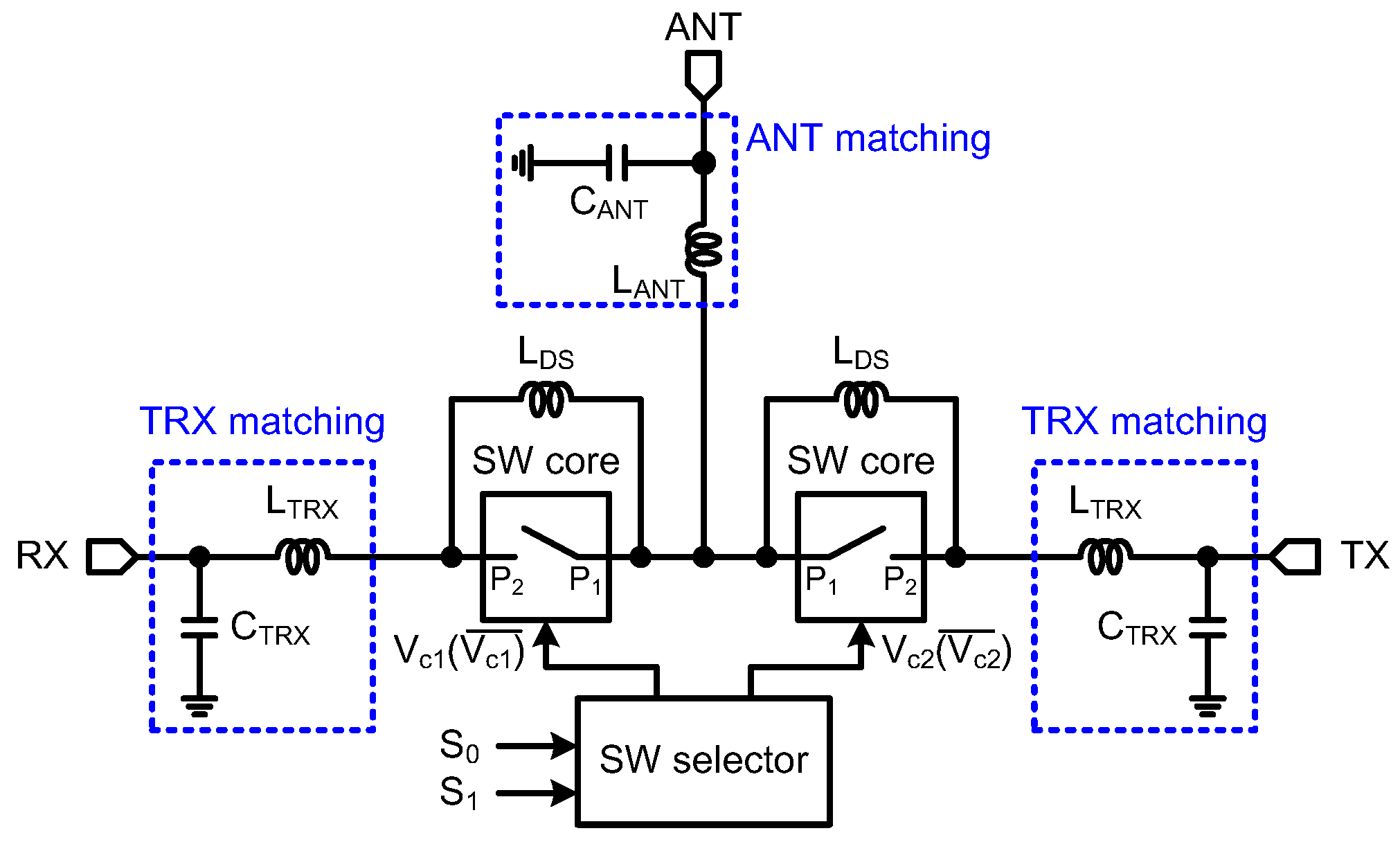
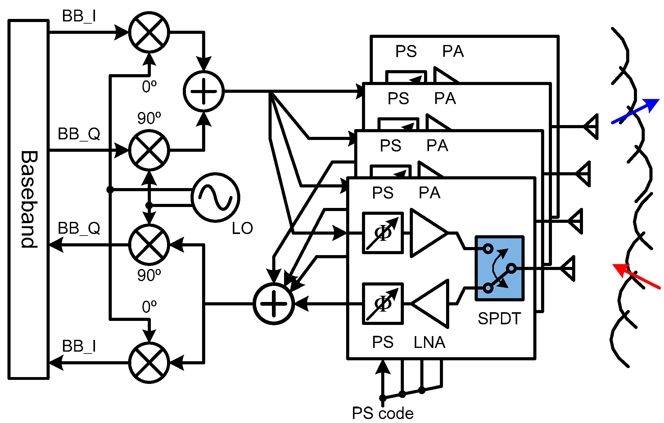
The SPDT switch selects the signal path between the antenna (ANT) and receiver (RX), or transmitter (TX), as shown in
Figure 1. The time to transmit and receive is divided by the switch, which is called the time-division duplex (TDD) method, in order to share the antenna with the TX and RX. Since the performance of the switch is critical to the noise figure of the RX, and the output power and efficiency of the TX, low insertion loss and high linearity are required. High isolation is also important, to prevent signal leakage from the TX to the RX. In addition to these characteristics, the area of the chip should be minimized, as many components are employed in a phased array antenna. Although there are many advantages associated with CMOS technology, such as low cost and high levels of integration, some challenges remain in implementing SPDT switches in this manner. The main challenge is achieving high isolation in the off state, and low insertion loss in the on state, simultaneously [
13,
14,
15]. The π-network has been widely employed at low frequencies, to enhance isolation, through the addition of shunt switches [
16,
17,
18,
19,
20]. However, since these shunt switches add additional parasitic capacitances to the signal path, the magnitude of the insertion loss increases, and the operating frequency decreases. Previous works have attempted to reduce parasitic capacitors by using a silicon-on-insulator (SOI) process or by adapting a switch biasing technique. Thus, resonant switch configurations using isolation enhancement (IE) inductors perform better at mm-wave frequencies [
21,
22,
23,
24]. Although the size is larger than π-network SPDT, it can be integrated, and the switch performance can be improved in certain mm-wave bands.
In this paper, two types of the SPDT switches for Ka-band phase-array transceivers are presented, in which the inductors are employed to enhance insertion loss and isolation by cancelling out the parasitic capacitances. The switches employ two different control methods, one using a single supply voltage, and one with dual supply voltages. The design of the mm-wave switch is detailed in
Section 2, along with the results of simulations. The results of experiments performed to characterize the SPDTs are described in
Section 3. A conclusion, as well as a summary of this paper, is detailed in
Section 4.
2. Design of the Single-Pole, Double-Throw (SPDT) Switch
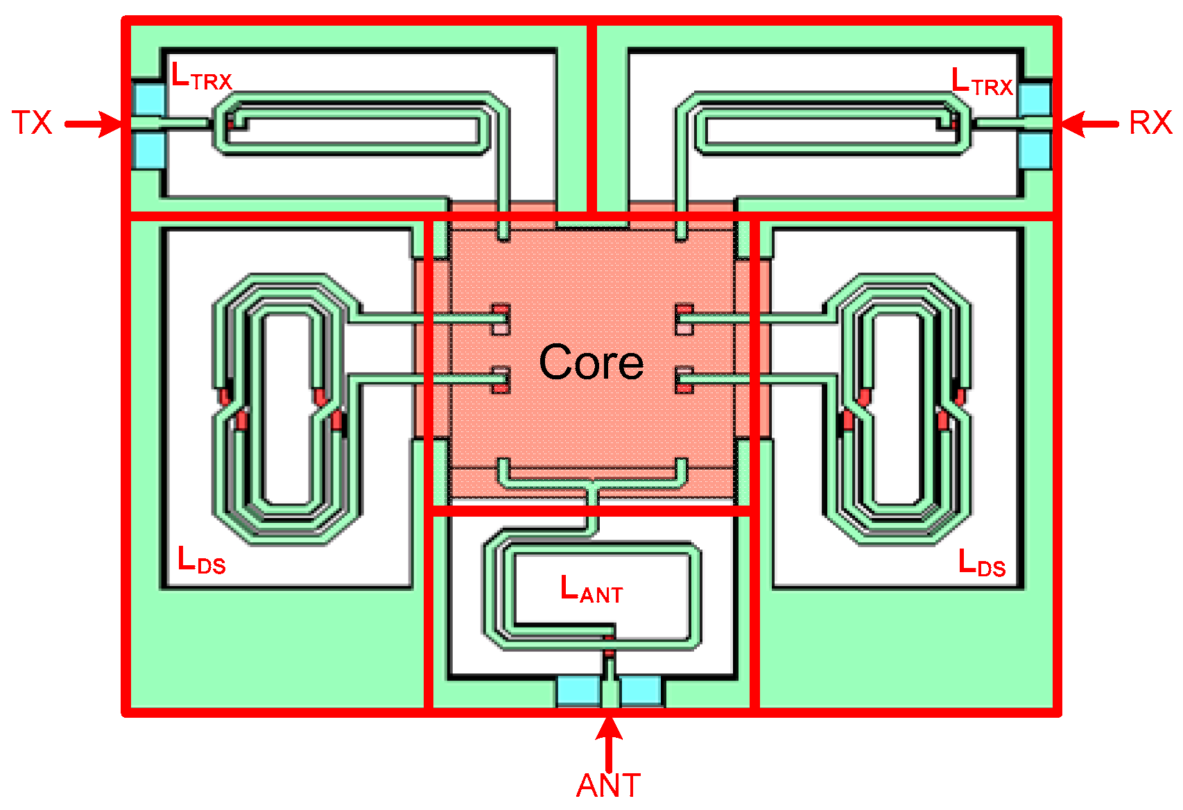
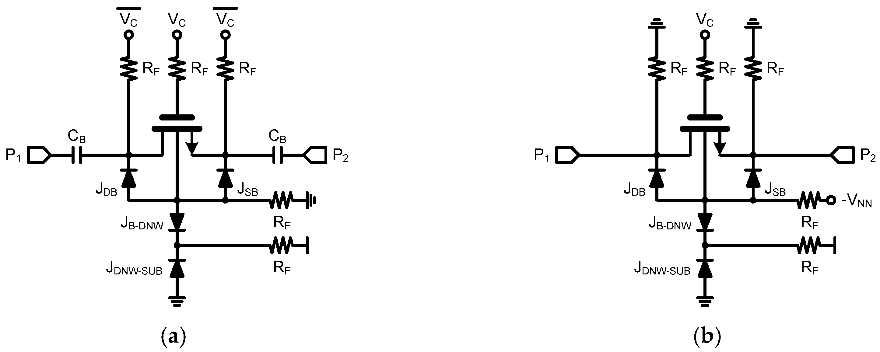
Figure 2 shows the block diagram of the SPDT, which is composed of two switch cores, isolation enhancement (IE) inductors,
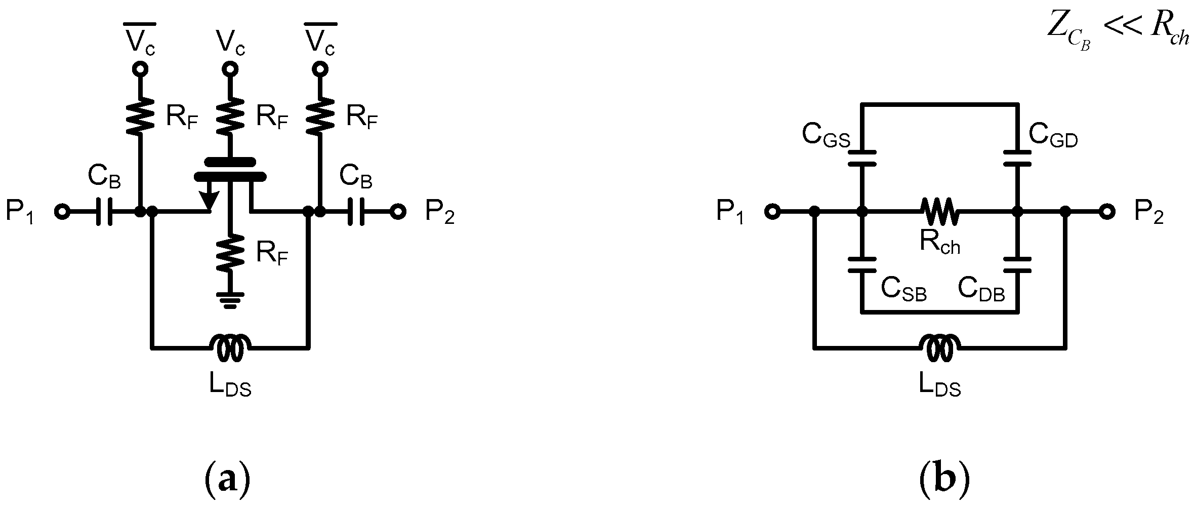
LDS to cancel out the parasitic capacitances of the switch cores, three impedance matching circuits for the RX, TX, and ANT ports, and a switch selector. Two types of switch cores were designed: The first switch core employs cross-biasing (CB) control with a single positive supply (
VDD) and ground voltage (0 V). The gate voltage is defined as
VC, and the drain and source voltage is defined as
, as shown in
Figure 3a. Since
varies according to the state of the switch controls S
1 and S
0, direct current (DC)-blocking capacitors,
CB, are added to the drain and source of the transistor. The other switch core uses dual supply biasing (DSB) control with positive and negative supply voltages (
VDD, −
VNN), as shown in
Figure 3b. These supply voltages control only the gate voltage,
VC, while the drain and source are grounded, i.e.,
VS,D = 0 V. The negative supply voltage is generated by an internal negative voltage generator (NVG).
The CB technique is to control gate and drain/source voltages simultaneously, by reversing their sign, to turn the switch on or off. The gate to drain/source voltage,
VGD,S becomes
VDD in the on state, and −
VDD in the off state. This negative
VGD,S can increase the TX-RX isolation, because the parasitic channel capacitances are reduced, in comparison to a normal biasing (NB) where
VGD,S = 0 V in the off state, due to the fixed drain and source voltage, i.e.,
VD,S = 0 V. With the DSB technique, the drain and source voltages are fixed to 0 V, as with the NB technique. However, by applying
VDD in the on state and −
VNN in the off state, a negative
VGD,S is applied, as in the CB technique. Thus, high TX-RX isolation is achieved. Since the DC-voltages of the drain and source are fixed to 0 V, no DC-blocking capacitors are required. All the deep-N-well (DNW) nodes are tied to
VDD, and the substrate node is connected to 0 V. The lowest voltage is good in terms of the power linearity [
18]. Thus, the body biases of the CB switch are set to 0 V, and the body biases for the DSB switch are set to −
VNN.
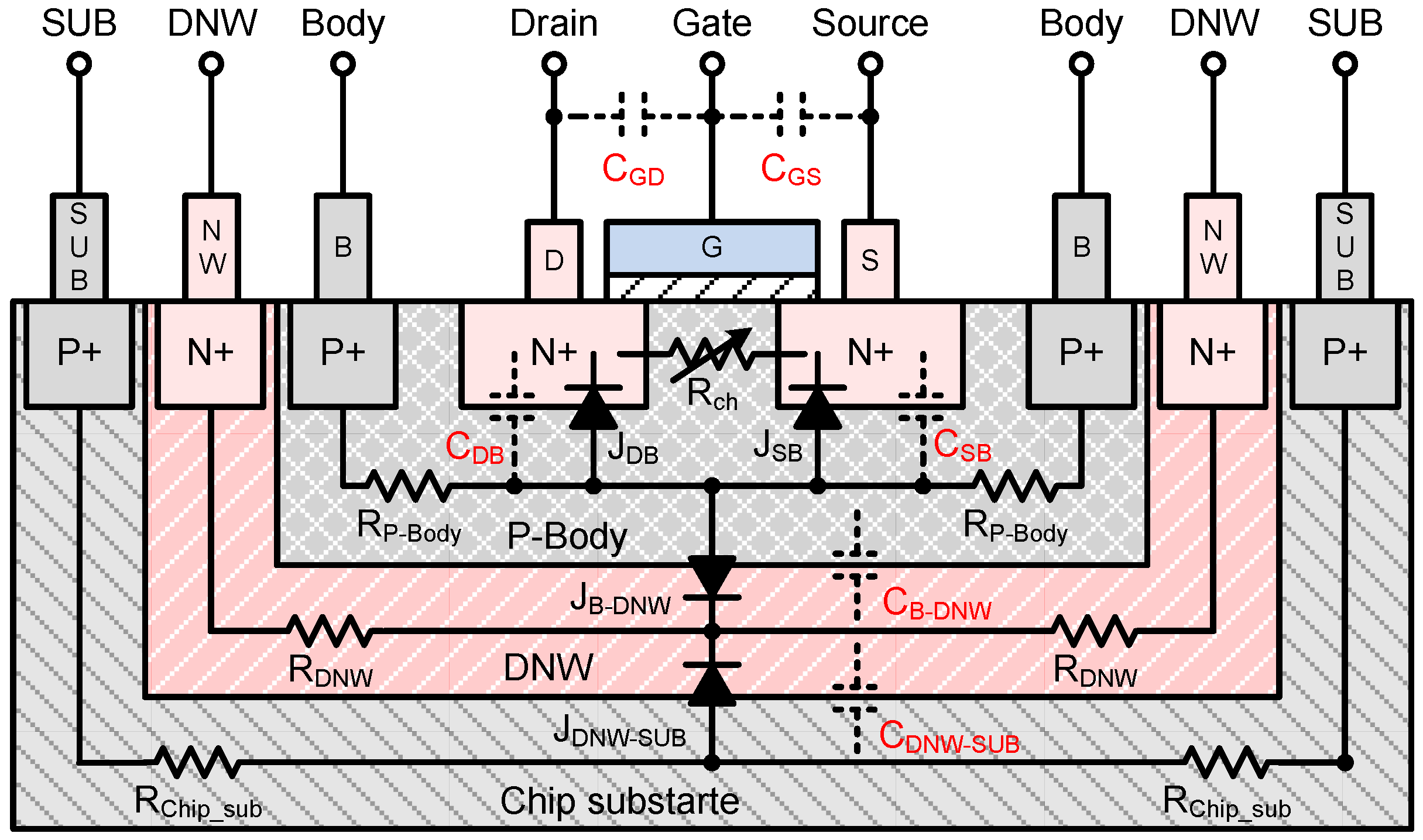
The substrate resistance of the CMOS process is as small as a few ohms. The noise and interference between transistors occur through the substrate, resulting in a decrease in signal-to-noise ratio (SNR). To reduce this effect, the P-type body of the transistor is separated to an N-type silicon layer, which is called deep-N-well (DNW), as shown in
Figure 4. The substrate of the transistor can be modeled as a P-N-P diode with a triple-well structure. In addition, the junction of the drain/source and the body can also be modeled as a diode. In
Figure 3 and
Figure 4, J
DB and J
SB are the junction diodes between the drain to body, and source to body, respectively. J
B-DNW is the junction diode between the body and DNW, and J
DNW-SUB is the junction diode between the DNW and chip substrate, respectively. If the voltage applied to the P-type silicon of the diode is higher than the voltage applied to the N-type silicon, it is conducted. However, in the opposite case, a current does not flow through the diode. It can be modeled as a reverse biased diode and a parallel parasitic capacitor. In
Figure 3 and
Figure 4,
CGS and
CGD are the parasitic capacitances between the gate and source, and the gate and drain, respectively.
CSB and
CDB are the junction capacitances between the source and body, and drain and body, respectively. The mm-wave-band signal can leak through parasitic capacitors which are caused by junction diodes. All signal paths through these junction diodes to ground (GND) or DC control voltage sources should be alternative current (AC)-floated to block unwanted signal leakages. Hence, 17.7 kΩ AC-floating resistors, R
F, of are used to the gate, drain, source, body, and DNW, as shown in
Figure 3.
The insertion loss and isolation of the switch core in
Figure 5a can be defined, according to the switch state, as |
S21|. The power delivered to the output port is determined by the impedances of the input and output ports, and the impedance of the source-drain channel (
Zsw). The magnitude of
S21 can be written as:
where
R0 is the input and output port impedance of 50 Ω [
17]. The IE inductor,
LDS, is introduced to remove the reactance component of the
Zsw, which is defined as:
In
Figure 5b,
Rch is the channel resistance of the transistor, which is greater than the impedance of the blocking capacitance,
CB, at operating frequency.
Ceq is the effective capacitance of the source and drain, which is expressed as,
The IE inductance is designed such that the inductor resonates at the operating frequency, to cancel the effective parasitic capacitance of the transistor.
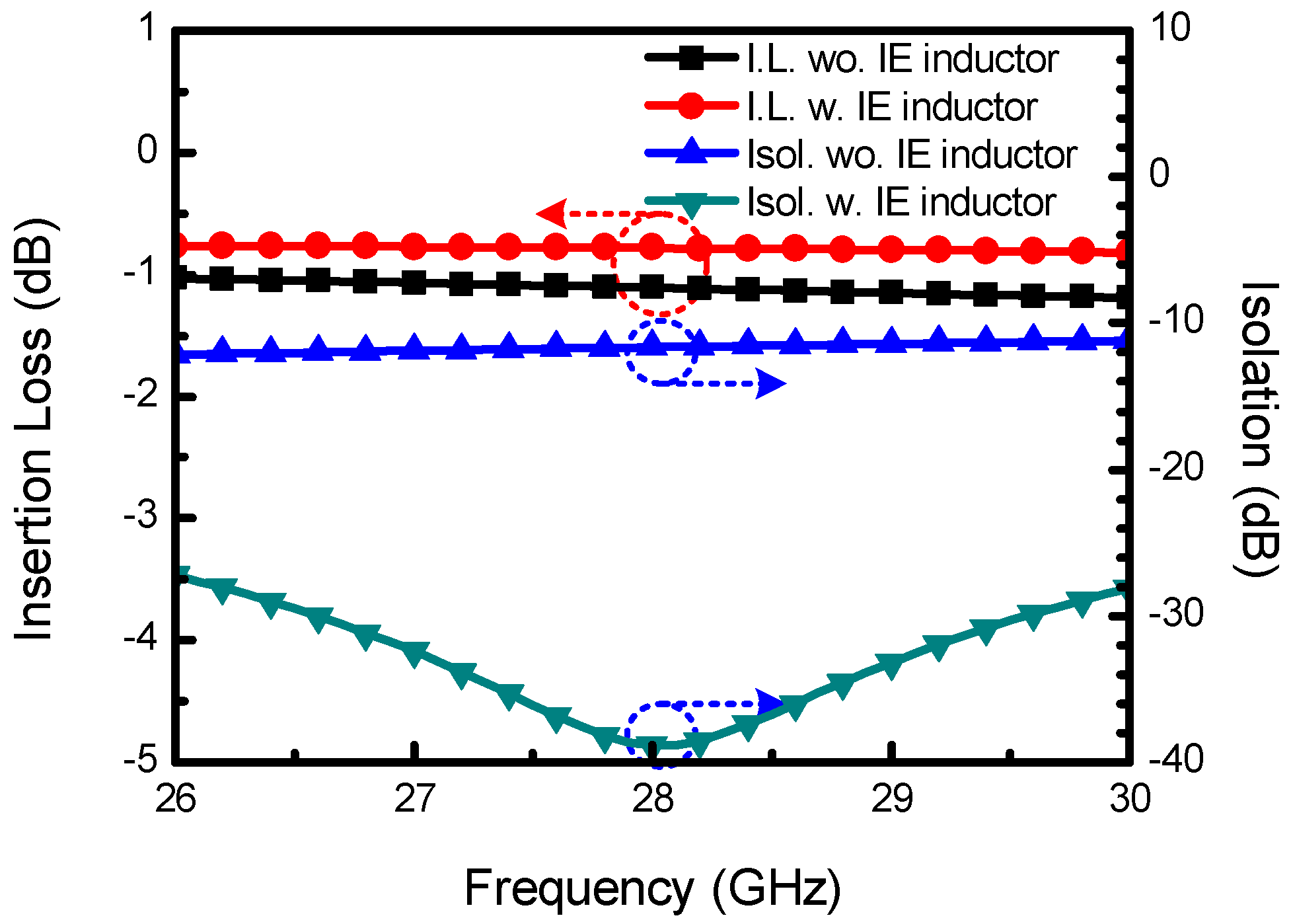
Figure 6 show the simulated insertion loss and isolation results of the CB switch core when all the inductors (
LDS,
LTRX,
LANT) are assumed to be ideal, with infinite Q-factor, and the total gate width of the switching transistor is 128 μm. Since the channel capacitance is canceled out at resonance, the isolation improves from −11 dB to −38 dB. The insertion loss also improves from −1.1 dB to −0.78 dB, due to the reduction of the channel capacitance. The switches are designed such that maximum isolation occurs at a target frequency of 28 GHz. Reducing the Q-factor of the IE inductor widens the switch bandwidth. However, the loss and isolation performance will decrease.
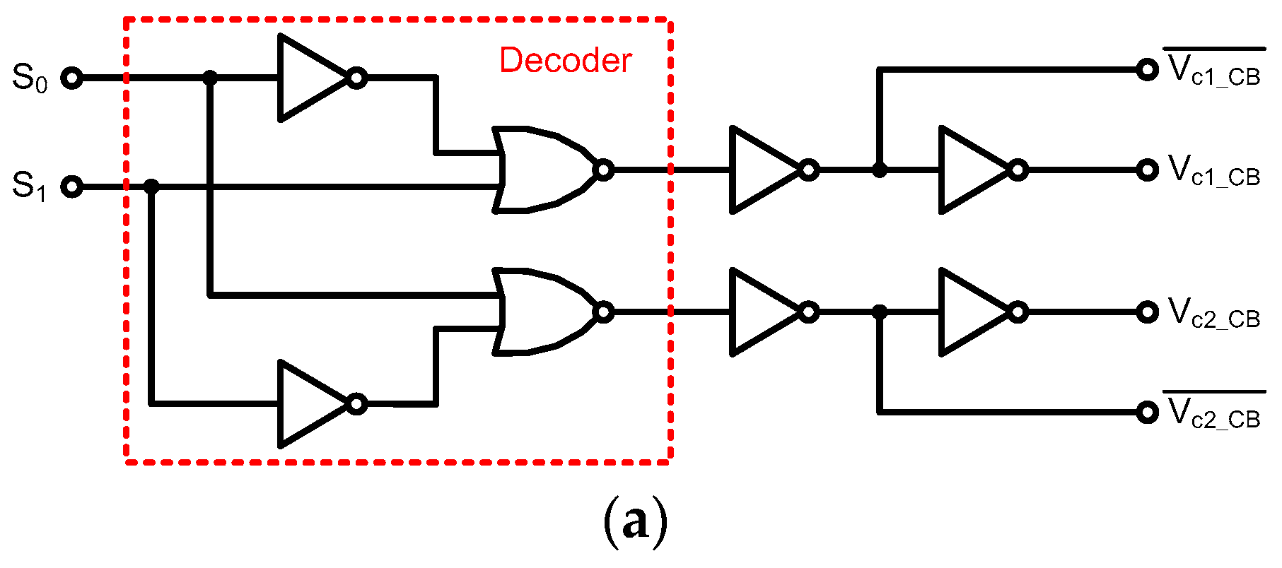
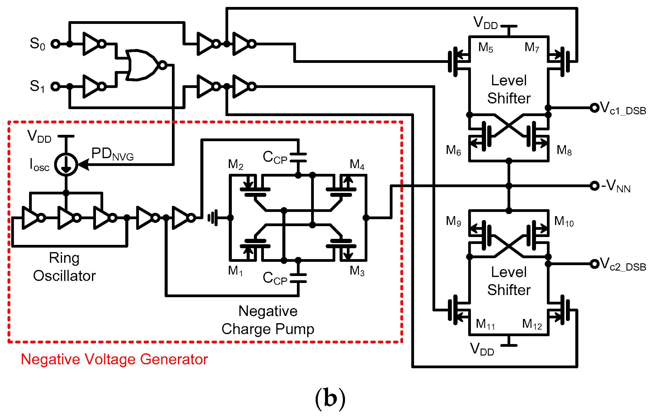
The CB selector in
Figure 7a consists of a two-bit decoder and inverters. The DSB selector in
Figure 7b requires a negative voltage, −
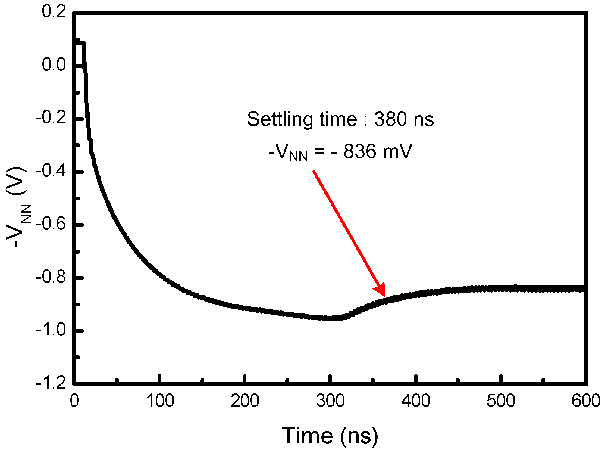
VNN, which is generated by an NVG. The NVG comprises a ring oscillator (OSC), a negative charge pump (CP), and two level shifters (LVS). The oscillator charges the capacitors,
CCP, which have a capacitance of 2.3 pF. Negative charges from the capacitors are transferred to the output node of the CP, generating −
VNN. The oscillation frequency of the OSC is set to 350 MHz. The estimated settling time is 380 ns, with −
VNN = −836 mV, as shown in
Figure 8. The level shifter changes the control voltages from
VDD and 0, to V
DD and −
VNN. The total static current consumption of the NVG is 150 μA.
Table 1 shows the switch control voltages according to the control mode and selector. For the CB switch selector, when both S
0 and S
1 are set high or low, the switch control voltages (
Vc1_CB and
Vc2_CB) become 0 V and block all RF signals. When S
0 is high and S
1 is low,
Vc1 is given by
VDD, and
Vc2 goes to 0 V. In contrast, when S
0 is low and S
1 is high,
Vc1 and
Vc2 become 0 V and
VDD, respectively. The DSB switch selector turns off the switch in two ways. When both S
0 and S
1 are set as low, the switch control voltages (
Vc1_DSB and
Vc2_DSB) become −
VNN. Alternatively, both S
0 and S
1 are set to high to turn off the NVG by blocking the oscillator current source and setting the control voltages to 0 V. When S
0 is high and S
1 is low,
Vc1 goes to
VDD and
Vc2 goes to −
VNN. In contrast, when S
0 is low and S
1 is high,
Vc1 and
Vc2 become −
VNN and
VDD, respectively.
The top view of the layout of the proposed CB and DSB SPDT switches, which displays the inductors and ground planes, is illustrated in
Figure 9. Both switches are identical, with the exception of the switch cores. All the active circuits are concentrated on the area of the core. Interference between the active devices and the inductors, through electromagnetic coupling, is minimized by separating the switch core from the inductors. The electro-magnetic (EM) characteristics were extracted using Sonnet, a 2.5-D EM simulator. Excluding the core circuit, all the inductors, metal connections, pads and ground planes except the core circuit were included in the EM simulation, to reduce the differences between the results from simulations and measurements. The inductance and Q-factor of
LDS were simulated as 643.5 pH and 21.6 at 28 GHz, respectively. The simulated inductance of
LTRX was 212.6 pH, and the Q-factor was 14.9, at 28 GHz. The simulated inductance and Q-factor of
LANT were 208.1 pH and 13.7 at 28 GHz, respectively.
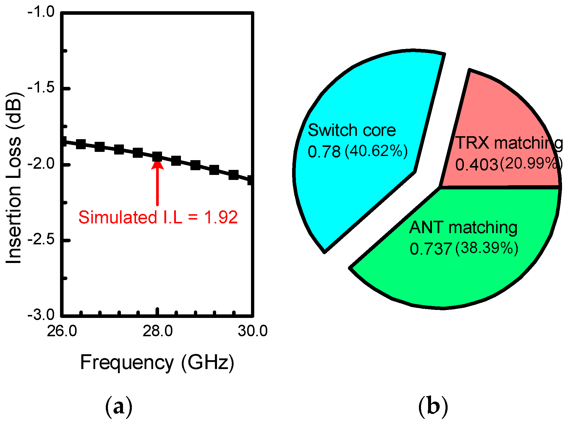
The contribution to the total insertion losses of the proposed switches was analyzed.
Figure 10a shows the simulated insertion loss of the CB SPDT switch. The insulation loss at 28 GHz is 1.92 dB, of which 40.6% occurred in the core cell, 21% occurred in the transceiver (TRX) matching circuit, and 38.4% occurred in the antenna matching circuit, as shown
Figure 10b.
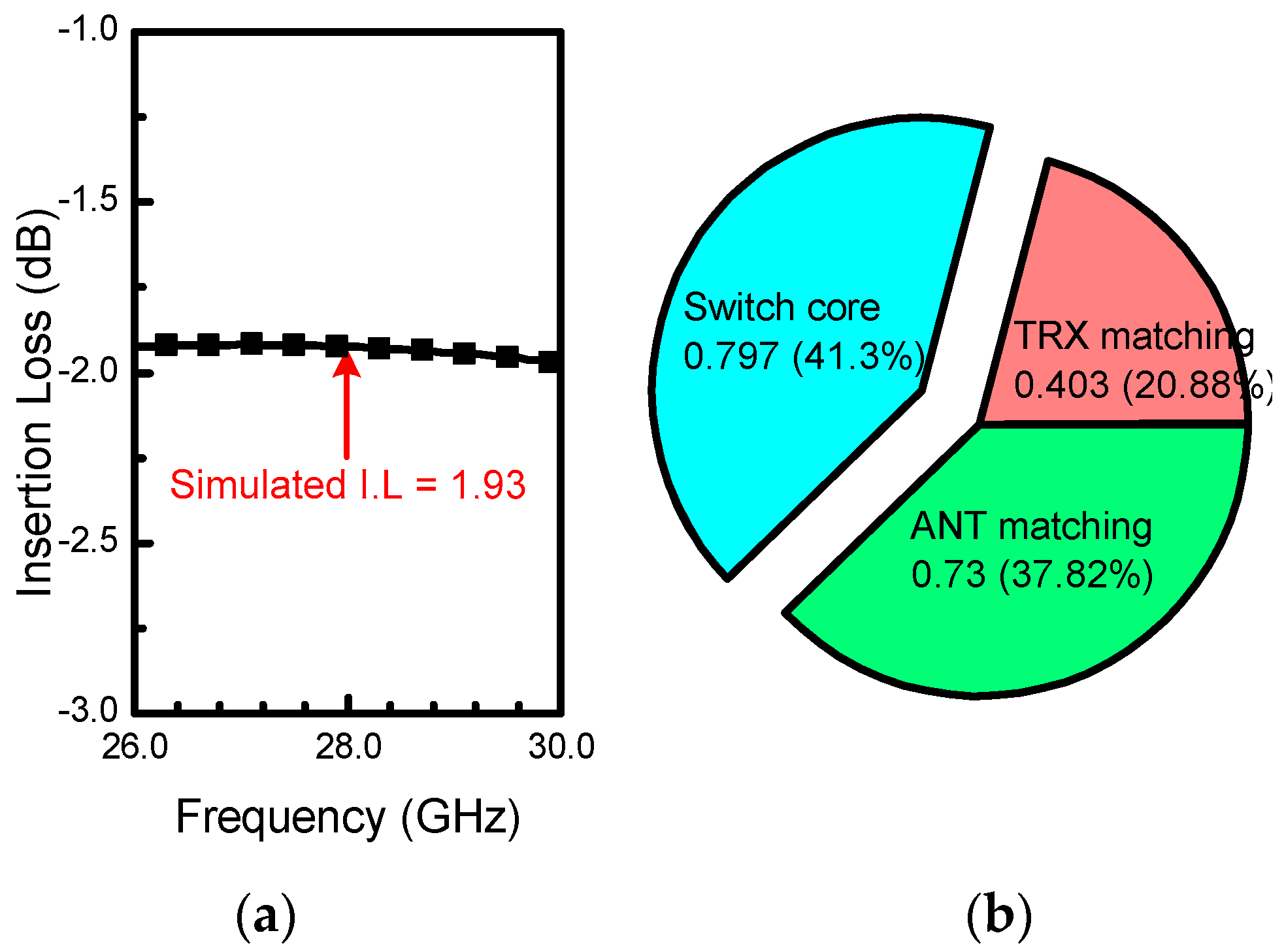
Figure 11a shows the simulation insertion loss of the proposed DSB SPDT switch. The insulation loss at 28 GHz is 1.93 dB, of which 41.3% occurred in the core cell, 20.9% occurred in the TRX matching circuit, and 37.8% occurred in the antenna matching circuit.
3. Implementation and Measured Results
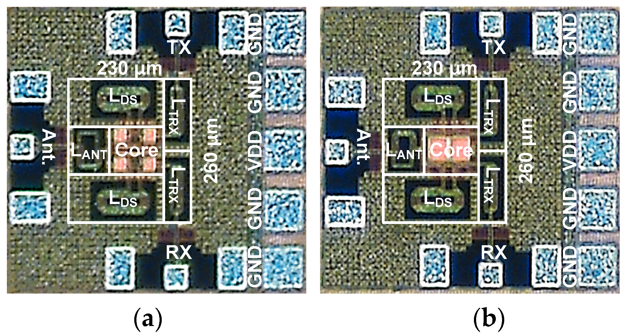
The proposed SPDT CMOS switches were fabricated using a 1P8M 65-nm CMOS process.
Figure 12a,b show microphotographs of the proposed Ka-band CB and DSB SPDT switches, which have identical pads and inductors—
LDS,
LANT, and
LTRX—and differ only in the core area. The total size of the chip, including all the pads, is 460 μm × 520 μm, and the area of the switch is 260 μm × 230 μm. All control pads, except the RF ports, were protected against electrostatic discharge (ESD). The test chips were glued to a printed circuit board and RF signals were connected directly to the measuring equipment using a ground–signal–ground (GSG) with a nominal impedance of 50 Ω. A supply voltage of 1 V was used for switch control. Small-signal measurements were recorded using a Keysight PNA E8363C network analyzer (Keysight, Santa Rosa, CA, U.S.). The linearity performances were measured by a Keysight N9030A spectrum analyzer (Keysight, Santa Rosa, CA, U.S.) and two E8257D signal sources (Keysight, Santa Rosa, CA, U.S.) with a power combiner.
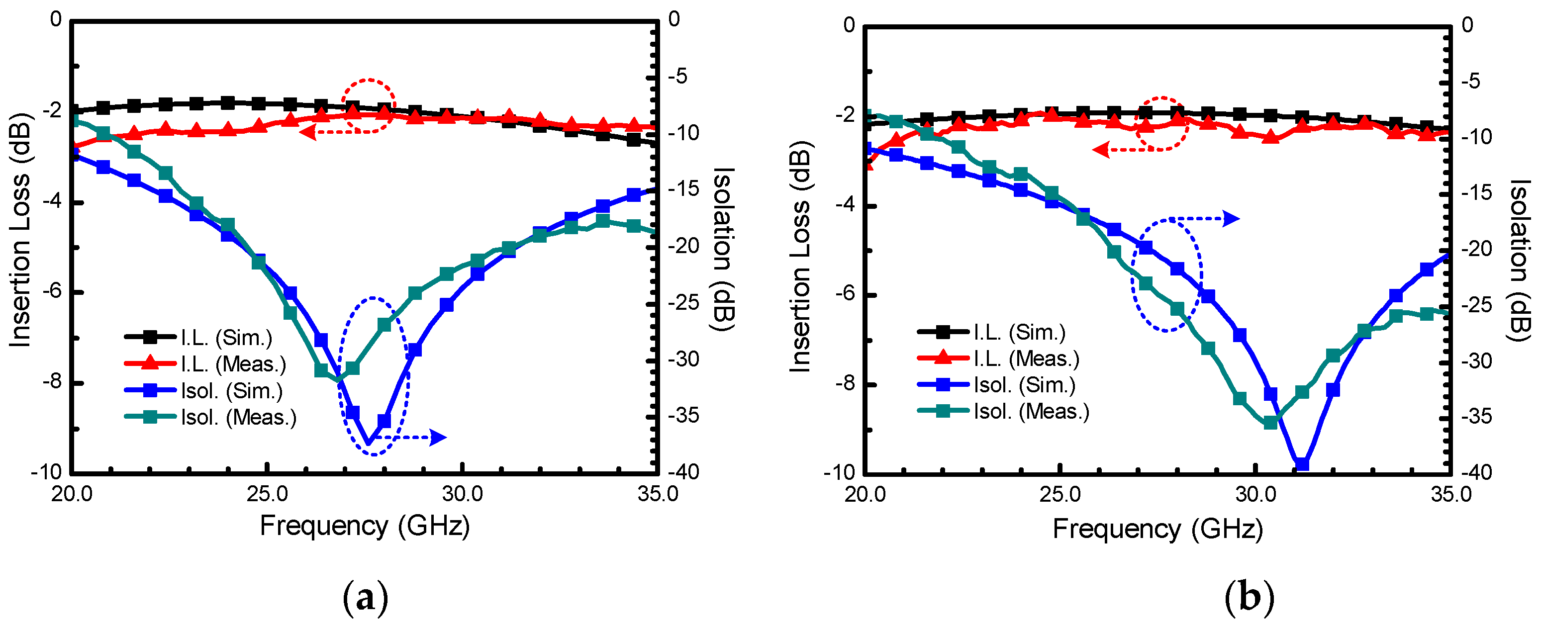
Figure 13 shows the simulated and measured insertion losses and isolation performances of the CB and DSB switches. The loss from the GSG pads and interconnection line between the pads and the core switch, which was compensated, was about 0.3 dB. The measured insertion losses of the CB switch was less than 2.3 dB between 25 GHz and 34 GHz. The minimum insertion loss was 2.1 dB at 28 GHz. The results from the measurements and simulations were in good agreement, with a difference of less than 0.6 dB. The maximum isolation measured was −32 dB, and achieved at 27 GHz, as intended. As shown in
Figure 13a, the measured isolation was greater than 19 dB, between 25 GHz and 34 GHz. With the DSB switch, between 25 GHz and 34 GHz, the measured insertion loss was less than 2.5 dB, which was slightly higher than with the CB switch, because the magnitude of the internally generated negative supply voltage,
VNN, was smaller than
VDD. The minimum insertion loss was 1.93 dB at 24.4 GHz. The results from the measurements and simulations were in good agreement, with a difference of less than 0.6 dB. As shown in
Figure 13b, the measured isolation was greater than 16 dB, between 25 GHz and 34 GHz. The minimum isolation measured was −34.81 dB, occurring at 30 GHz.
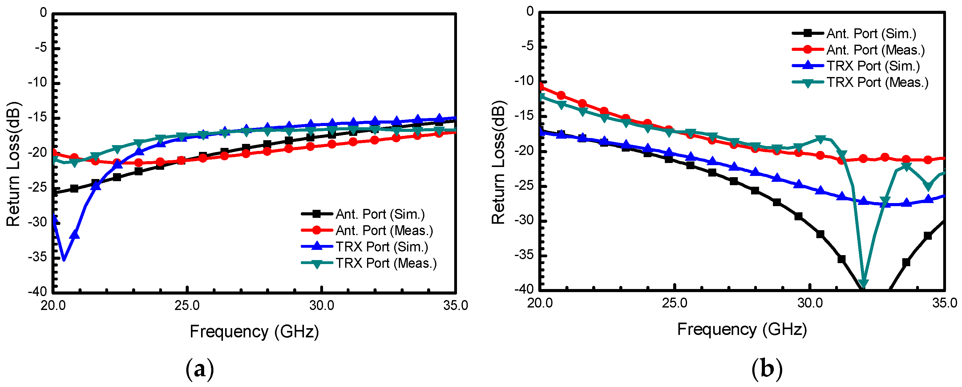
Figure 14a,b shows that both the CB and DSB switches had very low return losses, which were less than 17 dB in the operating bandwidth.
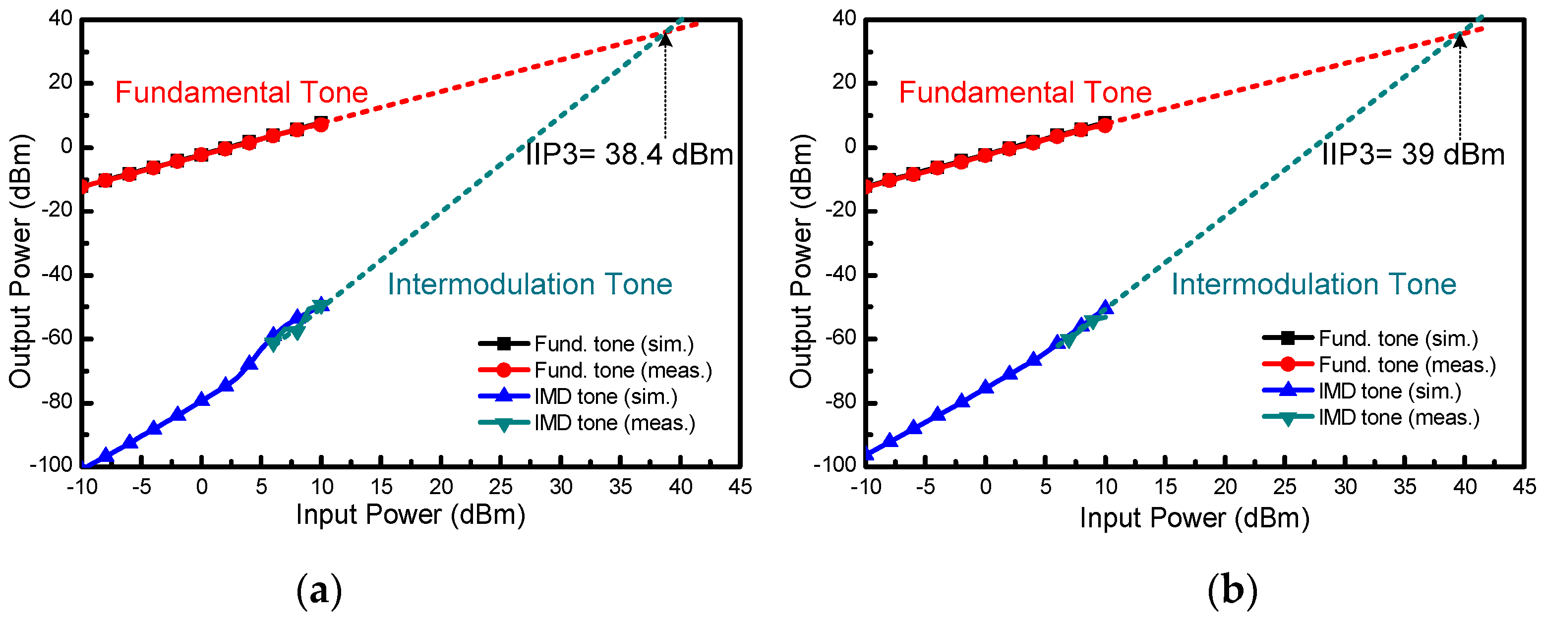
Figure 15a,b shows the output powers of the fundamental tones and third order intermodulation tones of the CB and DSB switches, respectively, according to the two-tone input power. Due to the lack of a high power mm-wave signal source, the input power was limited to 10 dBm. The third order input intercept (IIP3) points were calculated using two-tone signals at the frequency of 28 GHz. Each tone power was 7 dBm and the tone spacing was 100 MHz. The measured IIP3s of the CB and DSB switches were 38.4 dBm and 39 dBm, respectively.


