Repeater Insertion for Multi-Walled Carbon Nanotube Interconnects
by
 ,
,
Peng-Wei Liu
1, 
Zi-Han Cheng
1,
Wen-Sheng Zhao
1,*,
Qijun Lu
2,
Zhangming Zhu
2 and
Gaofeng Wang
1,* 1
Key Lab of RF Circuits and Systems of Ministry of Education, School of Electronics and Information, Hangzhou Dianzi University, Hangzhou 310018, China
2
School of Microelectronics, Xidian University, Xi’an 710071, China
*
Authors to whom correspondence should be addressed.
Appl. Sci. 2018, 8(2), 236; https://doi.org/10.3390/app8020236
Submission received: 17 December 2017
/
Revised: 20 January 2018
/
Accepted: 1 February 2018
/
Published: 4 February 2018
(This article belongs to the Special Issue Carbon Nanotubes for Interconnects)
Abstract
:Closed-form expressions for the optimized number and size of repeaters in multi-walled carbon nanotube (MWCNT) interconnects are presented. The contact resistance and inductive effects are taken into account. It is found that the propagation delay of MWCNT interconnects can be reduced effectively by inserting repeaters. However, the contact resistance has a significant influence on the optimized number and size of repeaters. Moreover, it is found that both the optimal number of repeaters and the minimum propagation delay are kept almost unchanged with the variation of carbon nanotube (CNT) kinetic inductance. The optimal number of repeaters in the MWCNT interconnect is much smaller than that in its Cu counterpart, thus saving chip area and power consumption.
1. Introduction
As the feature size of complementary metal-oxide semiconductor (CMOS)-integrated circuits continues to shrink, the interconnect dimensions are scaled down, which increases the electron scatterings at the surface and grain boundaries. Therefore, the interconnect delay increases dramatically and outweighs the gate delay, becoming the main bottleneck of improving the performance of modern integrated circuits [1]. More importantly, as predicted by the International Technology Roadmap for Semiconductors (ITRS), the current density will exceed the maximum allowable value of the conventional Cu interconnects within the next 5 years [2]. In order to solve such an issue, some innovative architectural concepts and materials are needed.
As alternative conductor materials, carbon nanomaterials, including carbon nanotubes (CNTs) and graphene, have aroused lots of interest due to their outstanding physical properties [3,4,5,6,7,8,9]. According to the number of carbon atom layers in a CNT wall, CNTs can be classified into single-walled CNTs (SWCNTs) and multi-walled CNTs (MWCNTs). SWCNTs can be either semiconducting or metallic, while MWCNTs are always metallic. Moreover, MWCNTs have a simpler fabrication process than SWCNTs due to easier control of the growth process, and under certain circumstances, MWCNTs possess a negative temperature coefficient on electrical resistance, which cannot be observed in SWCNTs [10,11].
Several research efforts have been made on the modeling and fabrication of MWCNT interconnects. Based on a physical model, it was found that the MWCNT conductivity increases with length and tends to be stable as the influence of contact resistance can be reduced by increasing the length [12]. As the length exceeds tens of micrometers, MWCNTs exhibit superior performance to their Cu and SWCNT counterparts, which makes MWCNTs suitable for the intermediate and global interconnect levels [13]. Although the complete multi-conductor transmission line proposed in [13] is accurate, it is time-consuming in dealing with complex MWCNT interconnects. Therefore, a simplified equivalent single-conductor (ESC) transmission line model was provided in [14] to reduce the computational complexity, with an expression for equivalent capacitance in the ESC model derived analytically. Furthermore, the impact of intershell tunneling conductance was investigated in [15,16], respectively, and it was found that the ESC model can provide an accurate prediction of time delay. Based on the ESC model, the robust design of the propagation characteristics and the crosstalk of MWCNT interconnects was carried out [17,18,19].
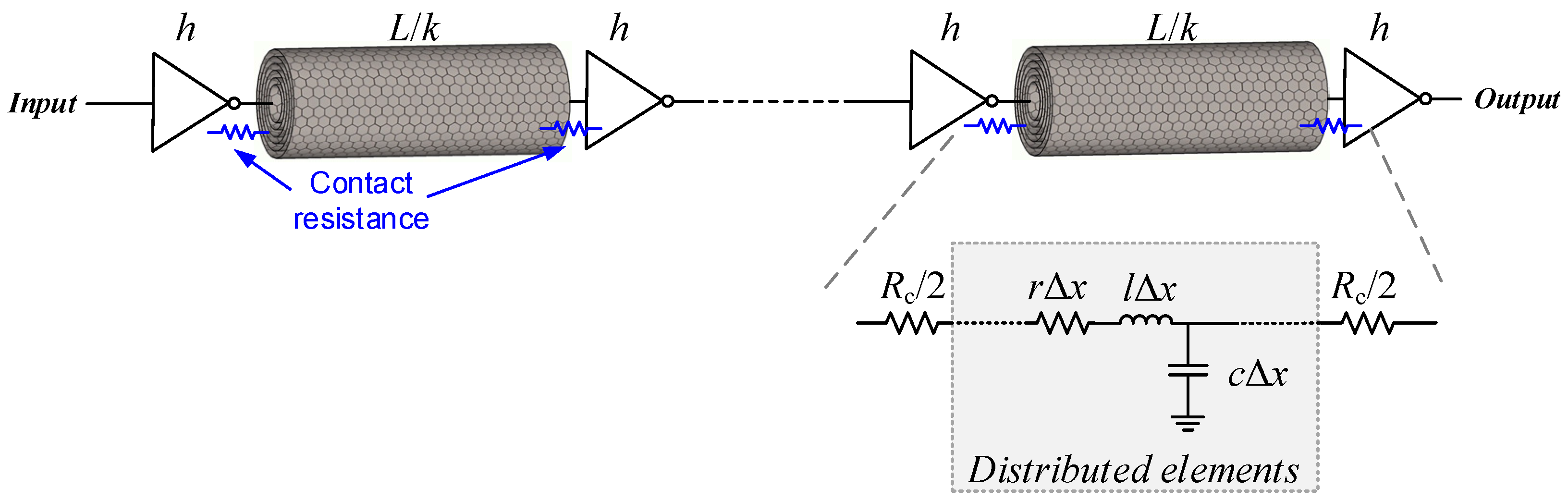
On the other hand, a repeater insertion methodology is essential for the implementation of high-performance VLSI designs. It is intuitive to insert some repeaters at intermediate- and global-level MWCNT interconnects, and a related investigation was carried out in [20]. As is well-known, however, contact resistance is inevitable in real-world applications of nanotube-like structures [21,22]. As shown in Figure 1, each inserted repeater in an MWCNT interconnect would, apparently, introduce new contact resistance, which would surely influence the propagation delay. The previous study [20] neglected the contact resistances induced by the inserted repeaters, thereby leading to overestimated electrical performance. The impact of contact resistance on optimal repeater insertion was studied for a monolayer SWCNT, an SWCNT bundle, and MWCNT interconnects in [23]. It was demonstrated that for MWCNT interconnects, the contact resistance must be taken into account when it exceeds a certain value. However, the study in [23] is just based on the resistance-capacitance (RC) model, and the optimal repeater size and number were obtained numerically. As indicated in [24], the measured CNT kinetic inductance may be 15 times larger than its theoretical value, and the inductive effect should be considered. Therefore, closed-form expressions for the optimized repeater size and number are desirable for MWCNT interconnects with the considerations of contact resistance and inductive effects, which is the motivation behind this study.
Based on the resistance-inductance-capacitance (RLC) model, this study focuses on the impacts of contact resistance on the optimal repeater size and number in intermediate- and global-level MWCNT interconnects at the 14 nm and 7 nm technology nodes. The rest of the paper is organized as follows. Section 2 introduces the ESC model of the MWCNT interconnects. Repeater insertion is studied in Section 3, with the closed-form expressions presented. Based on the proposed closed-form expressions, the optimal repeater insertion in MWCNT interconnects is investigated in Section 4. Some conclusions are finally drawn in Section 5.
2. ESC Model of the MWCNT Interconnect
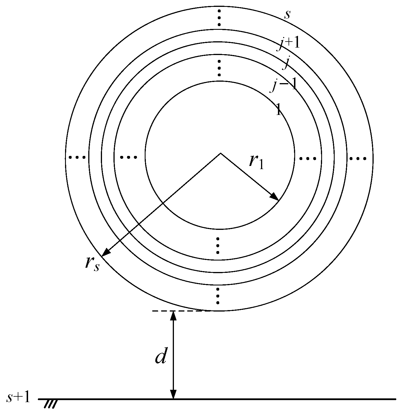
For easy reference and completion of the model, the ESC modeling procedure of an MWCNT interconnect is reproduced here. Figure 2 shows the schematic of an MWCNT placed above the ground plane. In the figure, and represent the outmost and innermost diameters, respectively, is the shell number, and is the distance between the MWCNT and ground plane. Here, the innermost shell diameter is assumed to be half of its outermost diameter, i.e., [25].
Supposing the spacing between adjacent shells in an MWCNT is , the number of the shells can be given as
where “Inter[·]” indicates that only the integer part is considered. The radius of the th shell is . As aforementioned, the MWCNT can be modeled as an ESC model [14] as shown in Figure 1. is the total terminal contact resistance, and it can be given as
where , is the Planck’s constant, is the electron charge, and is the imperfect contact resistance of the th shell. is the number of conducting channels of the th shell of an MWCNT, and it can be expressed as [12,26]
where and . is the equivalent quantum resistance per-unit-length (p.u.l.), and it is in parallel connection of the p.u.l. series resistances of each shell, i.e.,
where is the effective mean free path of the th shell in the MWCNT. is the equivalent p.u.l. inductance, and it can be obtained by
where is the p.u.l. equivalent kinetic inductance, and is the p.u.l. magnetic inductance of the external shell. According to [14], as the p.u.l. mutual inductance between adjacent shells is more than 3 orders of magnitude smaller than the p.u.l. kinetic inductance, it can be neglected. Therefore, the equivalent kinetic inductance is given as
where is the kinetic inductance per channel, and is the total number of conducting channels of the MWCNT. is the equivalent p.u.l. capacitance, and it can be given as [14]
The equivalent quantum capacitance is given as [14]
where is expressed in , is in nanometer, , , and . is the p.u.l. electrostatic capacitance of the external shell. The relationship between and can be expressed as
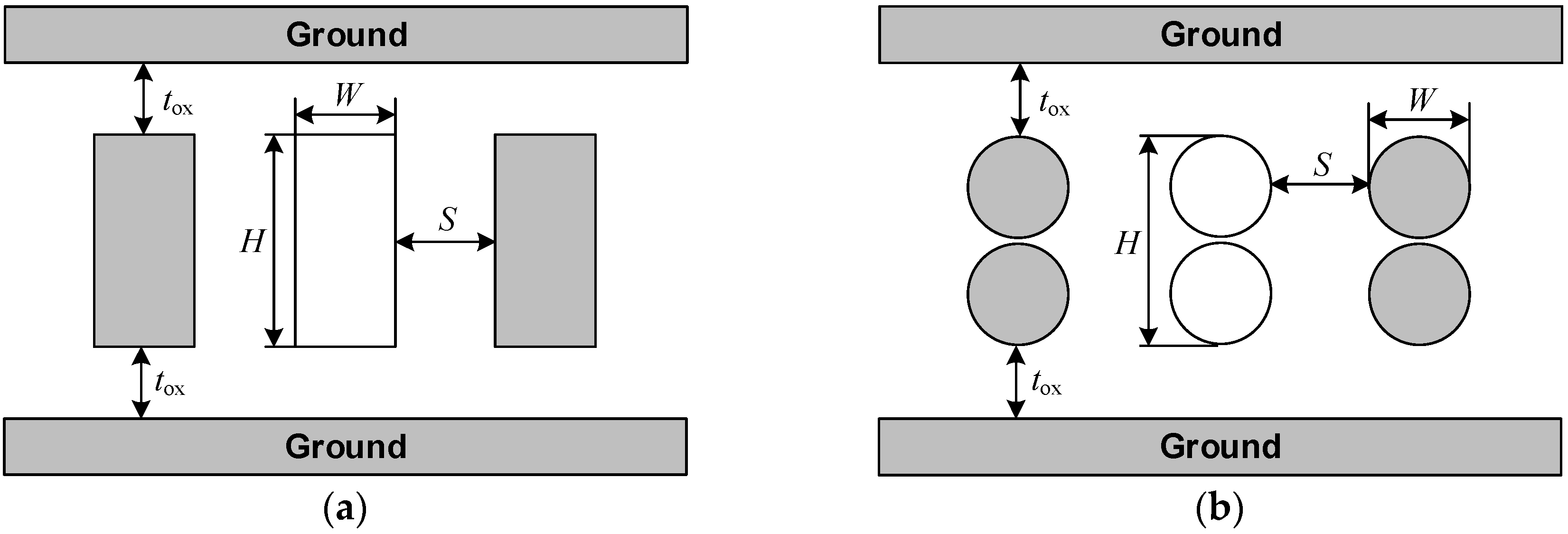
where and are the vacuum permeability and permittivity, respectively, and is the relative permittivity of the surrounding dielectric. Based on the typical interconnect configurations shown in Figure 3, the p.u.l. external capacitance is extracted by an electromagnetic simulator (e.g., ANSYS Maxwell). In this study, two technology nodes (i.e., the 14 nm and 7 nm technology nodes) are selected. In the figure, and are the interconnect width and height, respectively, is the aspect ratio, is the separation between adjacent interconnects, and is the thickness of the inter-layer dielectric (ILD). The geometrical and physical parameters, which are adopted from ITRS 2013, are listed in Table 1 [2]. Here, the aspect ratios of both the intermediate- and global-level MWCNT interconnects are assumed to be 2, as shown in Figure 3b. That is, two identical MWCNTs are stacked in parallel, and their gap is . It is evident that the external capacitance of the MWCNT interconnects is smaller than that of their Cu counterpart.
3. Repeater Insertion
As shown in Figure 1, a long MWCNT interconnect is divided into segments of by repeaters. Here, the inserted repeaters are assumed to be equispaced CMOS inverters, whose on resistance and input capacitance are obtained from the ITRS projection (see Table 1) [2]. In Figure 1, is the interconnect length, and is the ratio of the driver/load size to the minimum gate size. As aforementioned, each segment of the MWCNT interconnect can be modeled as an ESC model. The 50% propagation delay of one segment can be calculated by [27]
where , , and , and the three basic coefficients a1, a2, and a3 are the normalized ratios defined as follows [28]
where and are the output resistance and input capacitance of the minimum size gate, respectively, is the characteristic impedance, and is the time-of-flight [28].
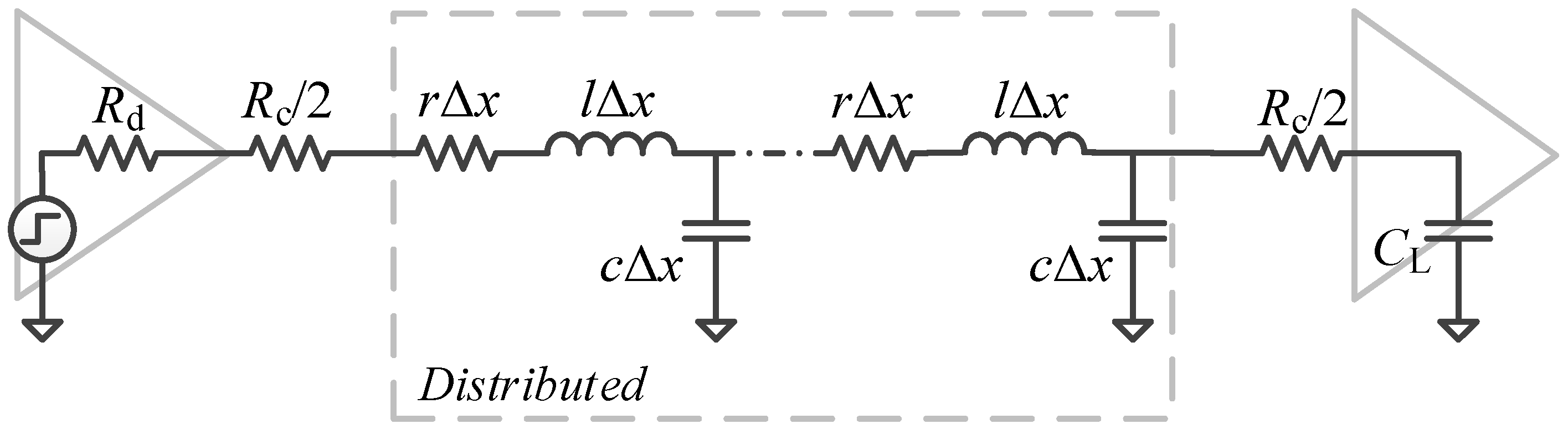
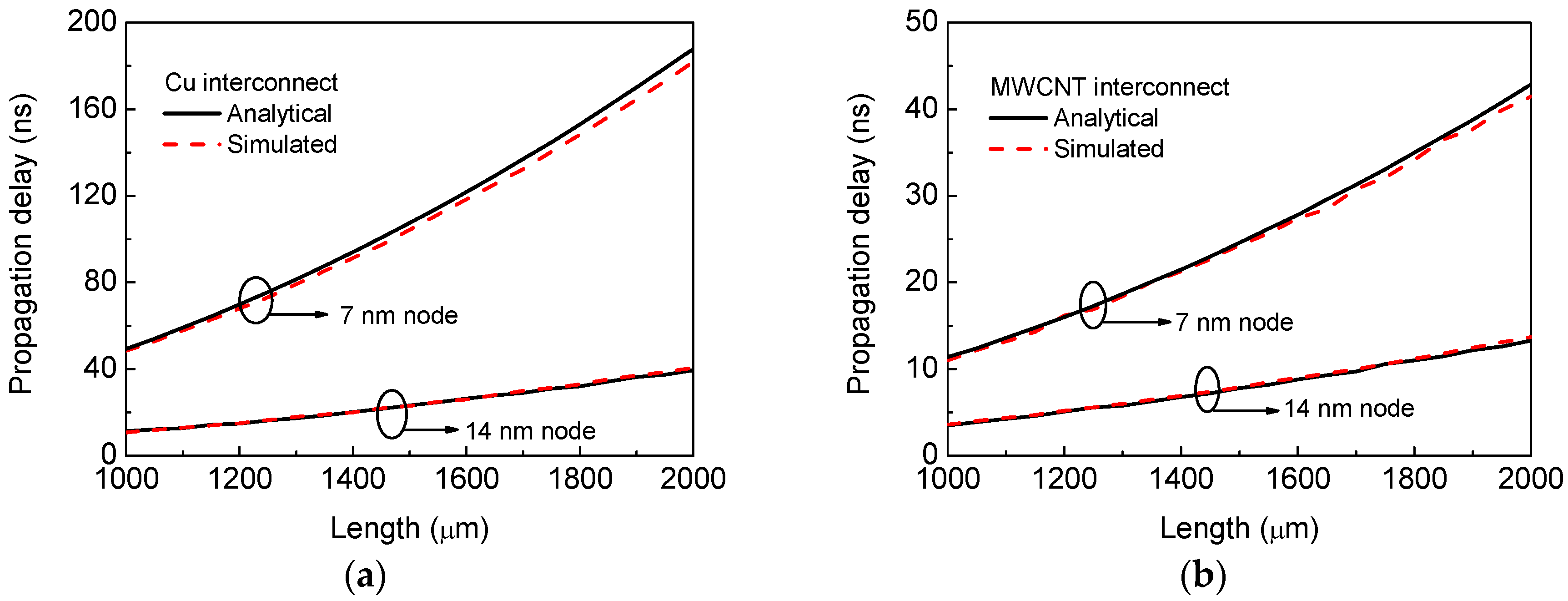
Based on the circuit model of a driver-interconnect-load (DIL) system in Figure 4, the accuracy of expression of the propagation delay can be examined. The driver and load are assumed to be 50 times the minimum sized gate for the intermediate-level interconnects, i.e., the driver resistance and load capacitance are and , respectively. Figure 5 shows the 50% propagation delays of the intermediate-level Cu and MWCNT interconnects at the 14 nm and 7 nm technology nodes. The solid lines are obtained analytically from (10), while the dashed lines denote the simulated results using a commercial circuit simulator (e.g., Keysight ADS). It can be seen that the analytical and simulated results agree well with each other. With the technology node advanced, the propagation delay increases significantly due to the increased resistivity. Moreover, it is known that an MWCNT has an extremely long mean free path, which is usually several micrometers and much larger than that of Cu wire (approximately 40 nm). Therefore, an MWCNT interconnect exhibits superior performance over its Cu counterpart, as shown in Figure 5. However, considering the contact resistance induced by the inserted repeaters, an MWCNT interconnect may lose its performance advantage, which will be discussed in the next section.
It is evident that that the time delay is a function of , , and , that is, . The total propagation delay of the MWCNT interconnects can be written as
According to [29], the repeater size and number of segments can be expressed as
where and are the correction factors. Substituting (15) and (16) into (14), the total propagation delay can be written as , where , , and . In real-world applications, must be smaller than the interconnect resistance . Otherwise, the fabrication process should be optimized first [22]. Therefore, is limited to [1, 1.4], and is in the range of [0, 10] [29]. After careful examination of the characteristic impedance of the MWCNT interconnects according to the geometrical and physical parameters adopted from the ITRS projection, is defined in the range of [0, 10]. In order to minimize the total propagation delay, and need to be solved simultaneously. By numerically solving these equations, and can be obtained. Using the multivariable curve fitting technique, the closed-form expressions of and are obtained and given as
The optimized repeater size and number of segments can be finally obtained by substituting (17) into (15) and (18) into (16), respectively. Then, the minimum propagation delay can be obtained by (14). Here, the optimal number of repeaters is denoted as , which is calculated as .
4. Results and Discussion
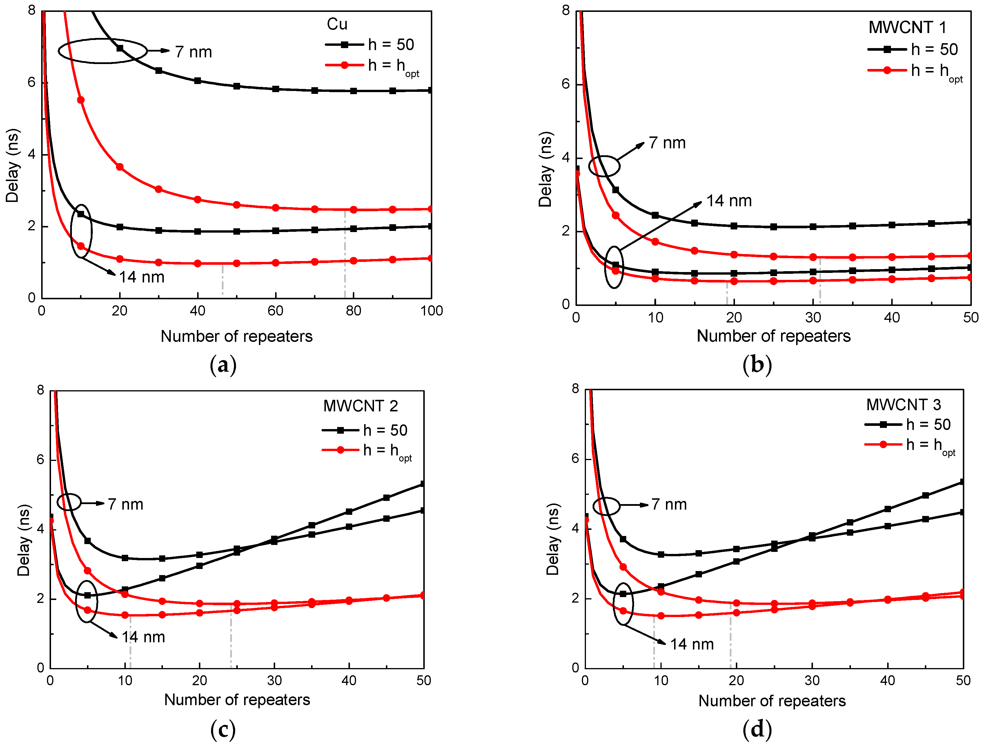
In order to clarify the influences of the contact resistance and CNT kinetic inductance, three types of MWCNT interconnects are taken into account, as listed in Table 2. Here, MWCNT 1 denotes an MWCNT interconnect with the minimum contact resistance , i.e., only the quantum contact resistance is considered. However, in real-world fabrication, imperfect contact resistance is inevitable. So, a contact resistance of is considered in the case of MWCNT 2. As aforementioned, the CNT kinetic inductance may be 15 times larger than its theoretical value. Therefore, MWCNT 3 represents an MWCNT interconnect with a contact resistance of and a kinetic inductance per channel of .
Figure 6 shows the propagation delay for 1000 μm-long intermediate-level Cu and MWCNT interconnects with the insertion of different numbers of repeaters. The optimal repeater size and the size of 50 times larger than the minimum gate size are considered. It can be seen that the minimum propagation delay is achieved when the repeaters of optimal size are inserted, and the estimation from the closed-form expressions is closed to the simulated optimal number of repeaters, as listed in Table 3. It is found that with the technology node advanced, the propagation delay increases significantly and more repeaters need to be inserted, which has an adverse effect on the chip area and power consumption. Therefore, a tapered buffer insertion should be employed to avoid large power dissipation [30,31], and further investigation should be conducted with constraints of both delay and power [32,33,34], which is the subject of our next study.
It is found that MWCNT interconnects require a much lower number of repeaters to optimize timing than Cu wires, which results in low complexity and power consumption. With the minimum contact resistance, MWCNT interconnects still exhibit superior performance over their Cu counterpart. However, the propagation delay of the MWCNT interconnects increases with the increasing contact resistance. At the 14 nm technology node, as the contact resistance increases to 10 kΩ, the minimum propagation delay of the MWCNT interconnect is 1.538 ns, which is much larger than that of Cu wire. Moreover, the increase in the CNT kinetic inductance has negligible influence on the optimal repeater size and number. So, the minimum propagation delay is kept almost unchanged with the variation of CNT kinetic inductance.
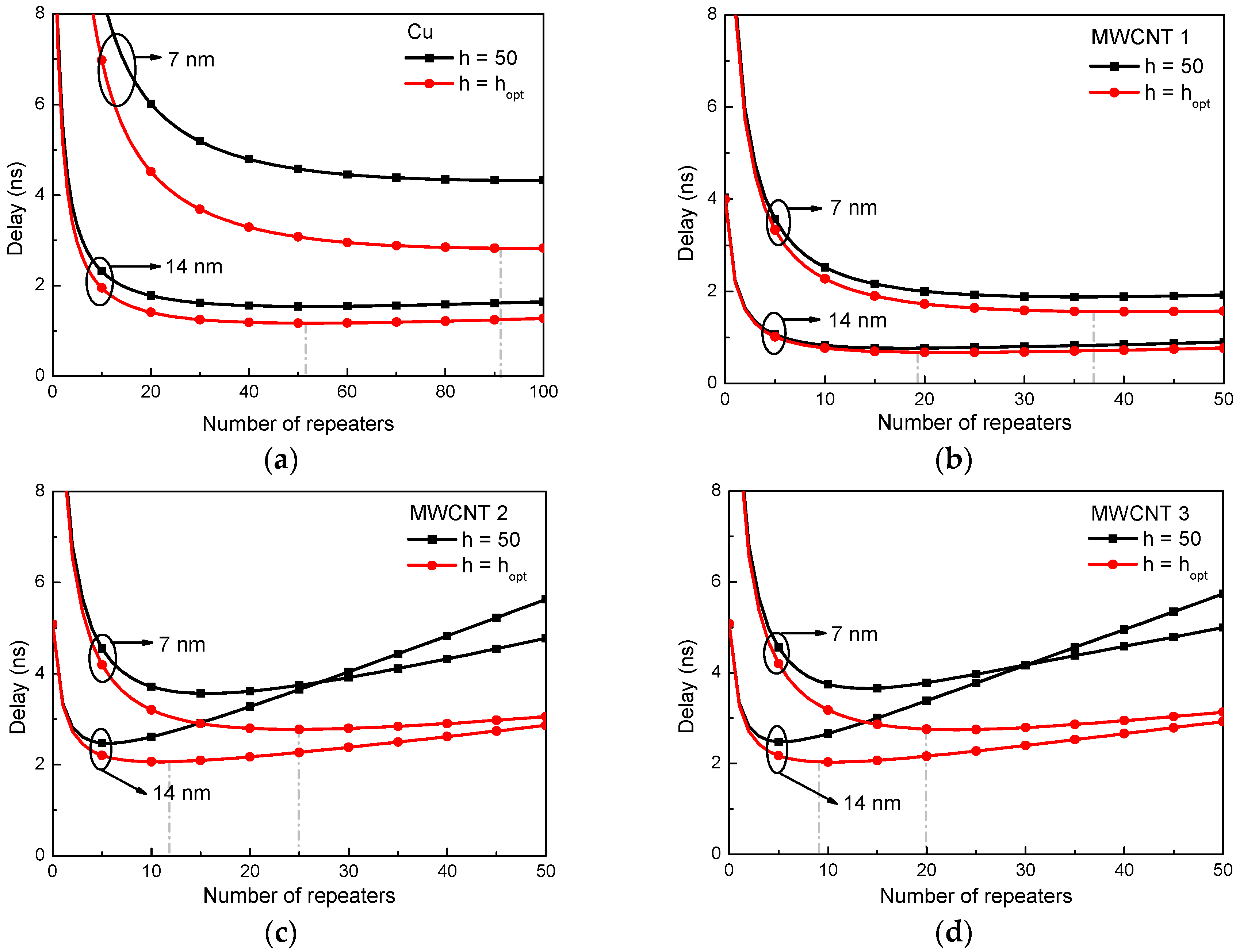
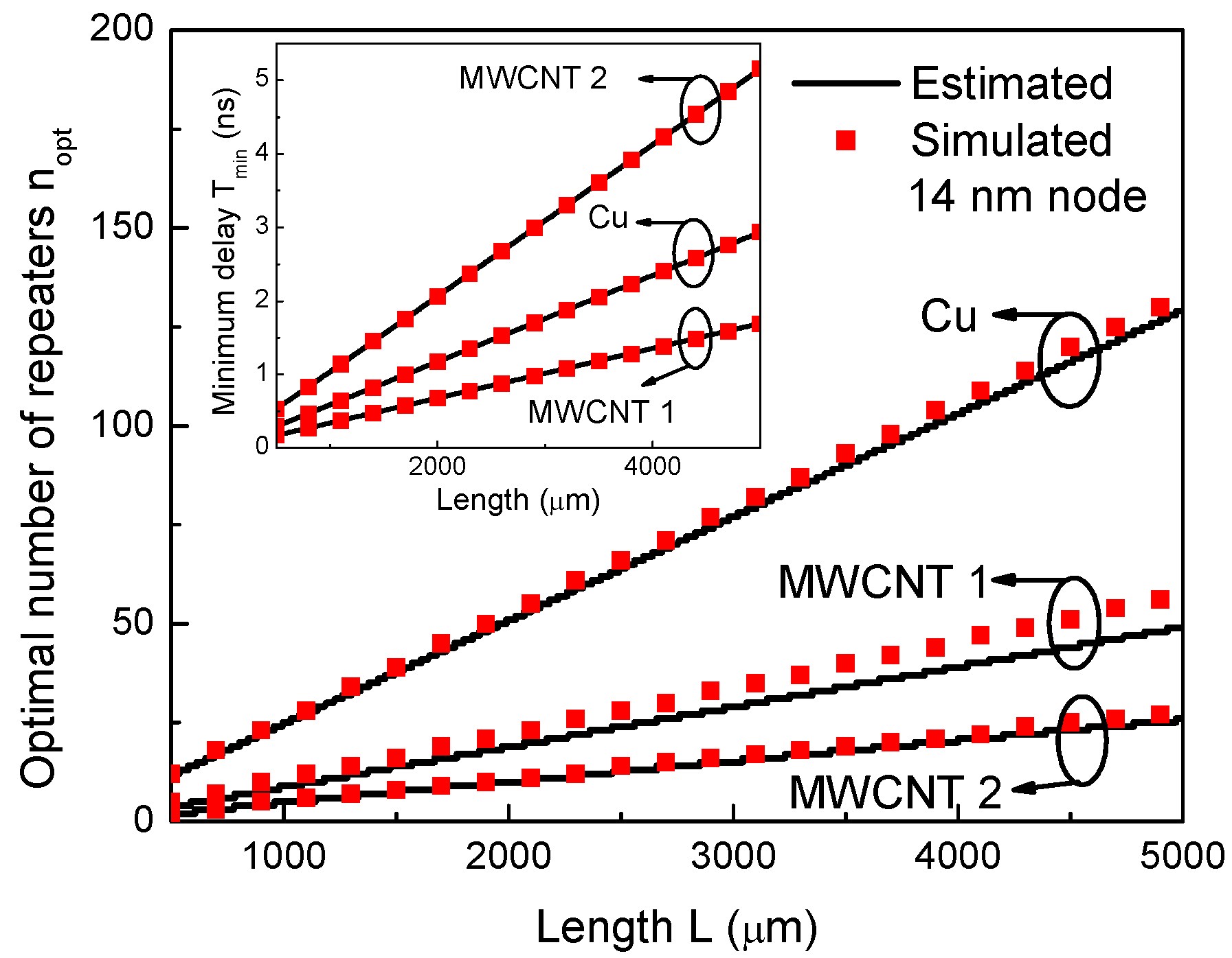
Further, the optimal repeater insertions in the global-level Cu and MWCNT interconnects are studied, as shown in Figure 7. The minimum propagation delay and optimal repeater size and number are summarized in Table 4. As a global-level interconnect has smaller resistivity than an intermediate one, it requires less repeaters to optimizing the timing. Similarly, the estimated repeater number agrees well with the simulated one. The propagation delay of the MWCNT interconnect decreases significantly with increasing contact resistance, implying that the impact of contact resistance cannot be simply neglected in the interconnect’s optimization and it is always essential to improve the fabrication process to reduce the contact resistance. Figure 8 compares the estimated and simulated values of the optimal repeater number and minimum propagation delay for the global interconnects at the 14 nm technology node. It is shown that the optimal repeater number increases linearly with increasing interconnect length.
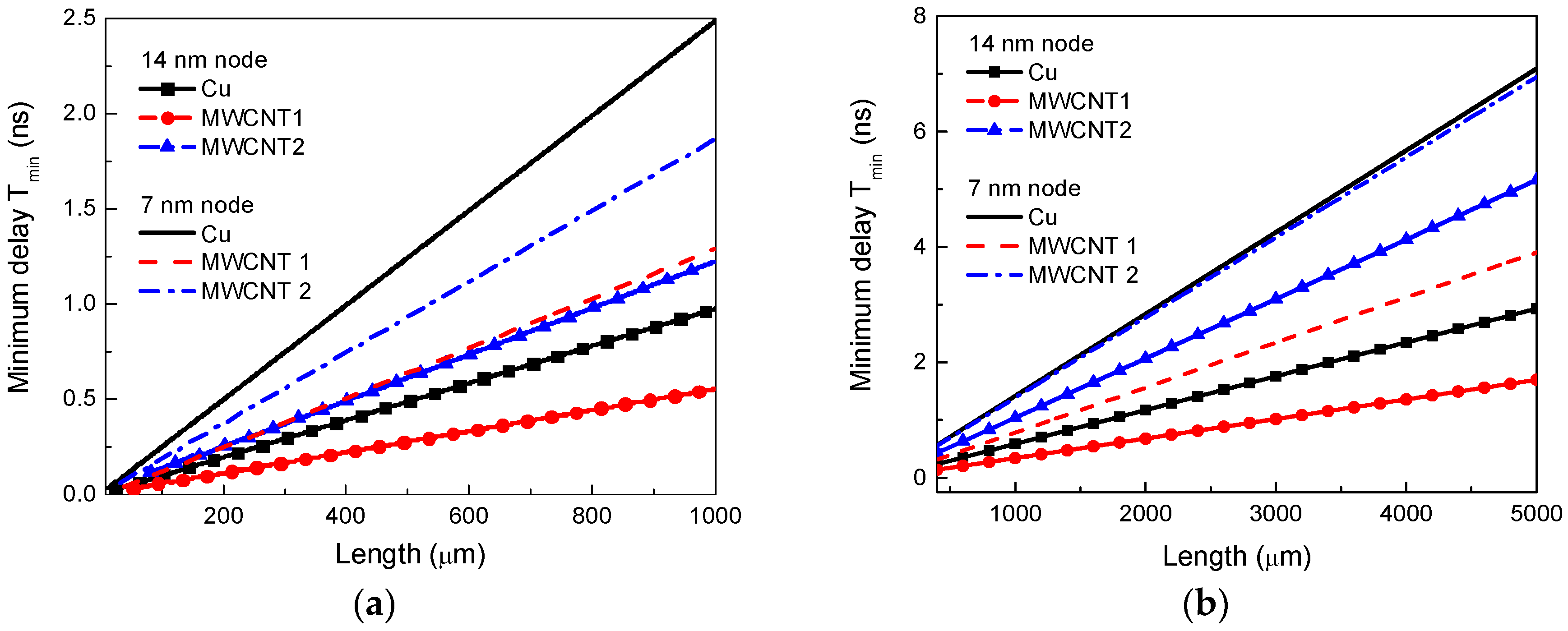
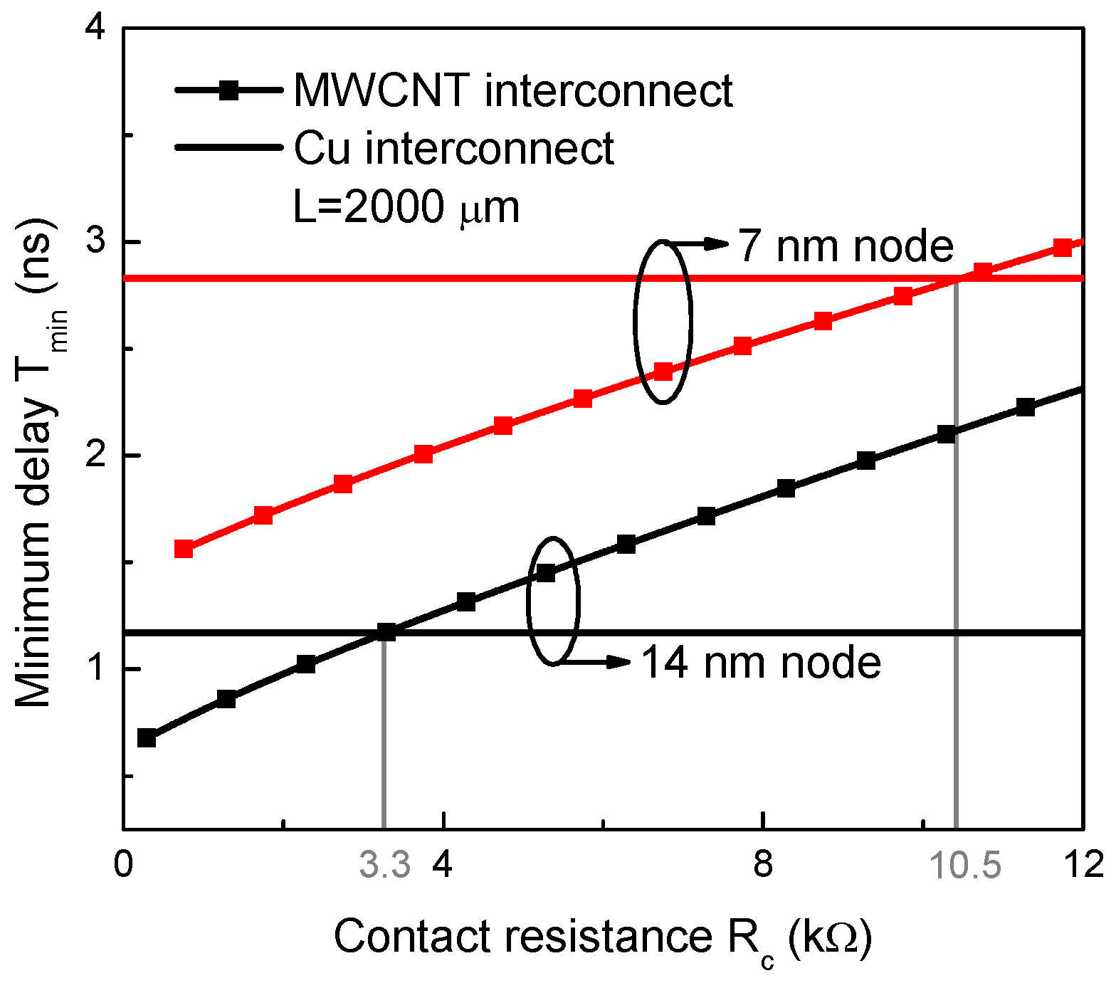
Based on the proposed fitting expressions, the minimum propagation delays of the intermediate and global interconnects are obtained as shown in Figure 9. It can be seen that the minimum propagation delay increases linearly with the length. With the minimum contact resistance, MWCNT interconnects can always provide a smaller delay than their Cu counterparts. However, as the contact resistance increases to , MWCNT interconnects would lose their edge at the 14 nm technology node, but still show superior performance over Cu at the 7 nm technology node. This can be explained as follows. As shown in Figure 10, at the 14 nm node, an MWCNT interconnect outperforms its Cu counterpart when the contact resistance is smaller than . With the technology scaling to 7 nm, the maximum tolerable contact resistance of the MWCNT interconnect is increased to 10.5 kΩ.
However, it is worth noting that even without the size effect and fabrication challenges at smaller nodes, the contact resistance of will be scaled up by 4 times from the 14 nm node to the 7 nm node. This is, at the 7 nm technology node, the contact resistance will increase to , which is already larger than the maximum tolerable contact resistance. In reality, the contact resistance scales up more drastically as the technology node goes down, which means more fabrication efforts need to be pursued such that an MWCNT interconnect can be able to outperform its Cu counterpart. In addition, the signal needs to go through back-end-of-line (BEOL) multilevel interconnect levels, from the top-level interconnect to the bottom-level buffer. After careful calculation, it is found that the resistance induced by multilevel interconnect levels is much smaller than the maximum tolerable contact resistance of the MWCNT interconnects [2]. Consequently, the conclusion of this study would not change even if the parasitic effects of these multilevel interconnect levels are taken into account.
5. Conclusions
In this study, closed-form expressions were presented for extracting the optimized size and number of repeaters in MWCNT interconnects. The contact resistance and the inductive effects were considered. It was demonstrated that neglecting the contact resistance would lead to significant error. To provide superior performance over the Cu wire, it is critical to reduce the contact resistance for the real-world applications of MWCNT interconnects. In particular, more fabrication efforts need to be pursued to reduce the contact resistance at more advanced technology nodes.
Acknowledgments
This study is supported by the National Natural Science Foundation of China under Grants 61504033 and 61411136003 and the Talent Project of Zhejiang Association for Science and Technology under Grant 2017YCGC012.
Author Contributions
All authors (listed below) have made a substantial contribution to this study. W.-S.Z. provided the concept and design of the study. P.-W.L., Z.-H.C., and Q.L. developed the simulation tool and processed the data. W.-S.Z. conducted the analysis of the results and wrote the article. Z.Z. and G.W. helped to revise the article.
Conflicts of Interest
The authors declare no conflict of interest.
References
- Davis, J.A.; Venkatesan, R.; Kaloyeros, A.; Beylansky, M.; Souri, S.J.; Benerjee, K.; Saraswat, K.C.; Rahman, A.; Reif, R.; Meindl, J.D. Interconnect limits on gigascale integration (GSI) in the 21st century. Proc. IEEE 2001, 89, 305–324. [Google Scholar] [CrossRef]
- International Technology Roadmap for Semiconductors, Edition 2013. Available online: http://www.itrs2.net/ (accessed on 1 August 2017).
- Li, H.; Xu, C.; Srivastava, N.; Banerjee, K. Carbon nanomaterials for next-generation interconnects and passives: Physics, status, and prospects. IEEE Trans. Electron Devices 2009, 56, 1799–1821. [Google Scholar] [CrossRef]
- Zhao, W.S.; Yin, W.Y. Carbon-based interconnects for RF nanoelectronics. Wiley Encycl. Electr. Electron. Eng. 2012, 1–20. [Google Scholar] [CrossRef]
- Close, G.F.; Wong, H.S.P. Assembly and electrical characterization of multiwall carbon nanotube interconnects. IEEE Trans. Nanotechnol. 2008, 7, 596–600. [Google Scholar] [CrossRef]
- Maffucci, A.; Miano, G. Electrical properties of graphene for interconnect applications. Appl. Sci. 2014, 4, 305–317. [Google Scholar] [CrossRef]
- Zhao, W.S.; Yin, W.Y. Comparable study on multilayer graphene nanoribbon (MLGNR) interconnects. IEEE Trans. Electromagn. Compat. 2014, 56, 638–645. [Google Scholar] [CrossRef]
- Cheng, Z.H.; Zhao, W.S.; Dong, L.; Wang, J.; Zhao, P.; Gao, H.; Wang, G. Investigation of copper-carbon nanotube composites as global VLSI interconnects. IEEE Trans. Nanotechnol. 2017, 16, 891–900. [Google Scholar] [CrossRef]
- Todri-Sanial, A.; Dijon, J.; Maffucci, A. Carbon Nanotubes for Interconnects; Springer: Zurich, Switwerland, 2017. [Google Scholar]
- Chiariello, A.G.; Maffucci, A.; Miano, G. Circuit models of carbon-based interconnects for nanopackaging. IEEE Trans. Compon. Packag. Manuf. Technol. 2013, 3, 1926–1937. [Google Scholar] [CrossRef]
- Maffucci, A.; Micciulla, F.; Cataldo, A.E.; Miano, G.; Bellucci, S. Modeling, fabrication, and characterization of large carbon nanotube interconnects with negative temperature coefficient of the resistance. IEEE Trans. Compon. Packag. Manuf. Technol. 2017, 7, 485–493. [Google Scholar] [CrossRef]
- Naeemi, A.; Meindl, J.D. Compact physical models for multiwall carbon-nanotube interconnects. IEEE Electron Device Lett. 2006, 27, 338–340. [Google Scholar] [CrossRef]
- Li, H.; Yin, W.Y.; Banerjee, K.; Mao, J.F. Circuit modeling and performance analysis of multi-walled carbon nanotube interconnects. IEEE Trans. Electron Devices 2008, 55, 1328–1337. [Google Scholar] [CrossRef]
- Sarto, M.S.; Tamburrano, A. Single-conductor transmission-line model of multiwall carbon nanotubes. IEEE Trans. Nanotechnol. 2010, 9, 82–92. [Google Scholar] [CrossRef]
- Forestiere, C.; Maffucci, A.; Maksimenko, S.A.; Miano, G.; Slepyan, G.Y. Transmission Line model for multiwall carbon nanotubes with intershell tunneling. IEEE Trans. Nanotechnol. 2012, 11, 554–564. [Google Scholar] [CrossRef]
- Tang, M.; Mao, J. Modeling and fast simulation of multiwalled carbon nanotube interconnects. IEEE Trans. Electromagn. Compat. 2015, 57, 232–240. [Google Scholar] [CrossRef]
- Lamberti, P.; Sarto, M.S.; Tucci, V.; Tamburrano, A. Robust design of high-speed interconnects based on an MWCNT. IEEE Trans. Nanotechnol. 2012, 11, 799–807. [Google Scholar] [CrossRef]
- D’Amore, M.; Sarto, M.S.; Tamburrano, A. Fast transient analysis of next-generation interconnects based on carbon nanotubes. IEEE Trans. Electromagn. Compat. 2010, 52, 496–503. [Google Scholar] [CrossRef]
- Liang, F.; Wang, G. Modeling of crosstalk effects in multiwall carbon nanotube interconnects. IEEE Trans. Electromagn. Compat. 2012, 54, 133–139. [Google Scholar] [CrossRef]
- Liang, F.; Wang, G.; Ding, W. Estimation of time delay and repeater insertion in multiwall carbon nanotube interconnects. IEEE Trans. Electron Devices 2011, 58, 2712–2720. [Google Scholar] [CrossRef]
- Franklin, D.; Chen, Z. Length scaling of carbon-nanotube transistors. Nat. Nanotechnol. 2010, 5, 858–862. [Google Scholar] [CrossRef] [PubMed]
- Chai, Y.; Hazeghi, A.; Takei, K.; Chen, H.Y.; Chan, P.C.H.; Javey, A.; Wong, H.S.P. Low-resistance electrical contact to carbon nanotubes with graphitic interfacial layer. IEEE Trans. Electron Devices 2012, 59, 12–19. [Google Scholar] [CrossRef]
- Zhao, W.S.; Wang, G.; Sun, L.L.; Yin, W.Y.; Guo, Y.X. Repeater insertion for carbon nanotube interconnects. Micro Nano Lett. 2014, 9, 337–339. [Google Scholar] [CrossRef]
- Plombon, J.J.; Obrien, K.P.; Gstrein, F.; Dubin, V.M.; Jiao, Y. High-frequency electrical properties of individual and bundled carbon nanotubes. Appl. Phys. Lett. 2007, 90, 063106. [Google Scholar] [CrossRef]
- Li, H.J.; Lu, W.G.; Li, J.J.; Bai, X.D.; Gu, C.Z. Multichannel ballistic transport in multiwall carbon nanotubes. Phys. Rev. Lett. 2005, 95, 086601. [Google Scholar] [CrossRef] [PubMed]
- Forestiere, C.; Maffucci, A.; Miano, G. On the evaluation of the number of conducting channels in multiwall carbon nanotubes. IEEE Trans. Nanotechnol. 2011, 10, 1221–1223. [Google Scholar] [CrossRef]
- Lu, Q.; Zhu, Z.; Yang, Y.; Ding, R. Analysis of propagation delay and repeater insertion in single-walled carbon nanotube bundle interconnects. Microelectron. J. 2016, 54, 85–92. [Google Scholar] [CrossRef]
- Venkatesan, R.; Davis, J.D.; Meindl, J.D. Compact distributed RLC interconnect models—Part IV: Unified models for time delay, crosstalk, and repeater insertion. IEEE Trans. Electron Devices 2003, 50, 1094–1102. [Google Scholar] [CrossRef]
- Ismail, Y.I.; Friedman, E.G. Effects of inductance on the propagation delay and repeater insertion in VLSI circuits. IEEE Trans. Very Large Scale Integr. Syst. 2000, 8, 195–206. [Google Scholar] [CrossRef]
- Li, N.C.; Haviland, G.L.; Tuszynski, A.A. CMOS tapered buffer. IEEE J. Solid State Circuits 1990, 25, 1005–1008. [Google Scholar] [CrossRef]
- Saini, S. Low Power Interconnect Design; Springer: New York, NY, USA, 2017. [Google Scholar]
- Adler, V.; Friedman, E.G. Repeater design to reduce delay and power in resistive interconnect. IEEE Trans. Circuits Syst. II Analog Digit. Signal Process. 1998, 45, 607–616. [Google Scholar] [CrossRef]
- Banerjee, K.; Mehrotra, A. A power-optimal repeater insertion methodology for global interconnects in nanometer designs. IEEE Trans. Electron Devices 2002, 49, 2001–2007. [Google Scholar] [CrossRef]
- Chen, G.; Friedman, E.G. Low-power repeaters driving RC and RLC interconnects with delay and bandwidth constraints. IEEE Trans. Very Large Scale Integr. Syst. 2006, 14, 161–172. [Google Scholar] [CrossRef]
Figure 1.
Repeater insertion in a long multi-walled carbon nanotube (MWCNT) interconnect and the equivalent single-conductor (ESC) model for one segment of the MWCNT interconnect.
Figure 1.
Repeater insertion in a long multi-walled carbon nanotube (MWCNT) interconnect and the equivalent single-conductor (ESC) model for one segment of the MWCNT interconnect.

Figure 2.
Geometrical configuration of the cross-section of an MWCNT.

Figure 3.
Cross-sectional views of (a) Cu and (b) MWCNT interconnect configurations in an advanced integrated circuit design.
Figure 3.
Cross-sectional views of (a) Cu and (b) MWCNT interconnect configurations in an advanced integrated circuit design.

Figure 4.
Distributed circuit model of a driver-interconnect-load (DIL) system.

Figure 5.
Propagation delays versus length in the intermediate-level (a) Cu and (b) MWCNT interconnects.
Figure 5.
Propagation delays versus length in the intermediate-level (a) Cu and (b) MWCNT interconnects.

Figure 6.
Propagation delays versus number of repeaters for 1000-μm-long intermediate-level Cu and MWCNT interconnects. (a) Cu; (b) MWCNT 1; (c) MWCNT 2; and (d) MWCNT 3.
Figure 6.
Propagation delays versus number of repeaters for 1000-μm-long intermediate-level Cu and MWCNT interconnects. (a) Cu; (b) MWCNT 1; (c) MWCNT 2; and (d) MWCNT 3.

Figure 7.
Propagation delays versus number of repeaters for 2000-μm-long global-level Cu and MWCNT interconnects. (a) Cu; (b) MWCNT 1; (c) MWCNT 2; and (d) MWCNT 3.
Figure 7.
Propagation delays versus number of repeaters for 2000-μm-long global-level Cu and MWCNT interconnects. (a) Cu; (b) MWCNT 1; (c) MWCNT 2; and (d) MWCNT 3.

Figure 8.
Optimal number of repeaters (Inset: minimum propagation delay) versus length for global-level Cu and MWCNT interconnects at the 14 nm technology node.
Figure 8.
Optimal number of repeaters (Inset: minimum propagation delay) versus length for global-level Cu and MWCNT interconnects at the 14 nm technology node.

Figure 9.
Minimum propagation delays versus length for (a) intermediate- and (b) global-level Cu and MWCNT interconnects.
Figure 9.
Minimum propagation delays versus length for (a) intermediate- and (b) global-level Cu and MWCNT interconnects.

Figure 10.
Minimum propagation delay versus contact resistance for 2000-μm-long global-level Cu and MWCNT interconnects.
Figure 10.
Minimum propagation delay versus contact resistance for 2000-μm-long global-level Cu and MWCNT interconnects.


Table 1.
Geometrical and physical parameters at the 14 nm and 7 nm technology nodes.
| Technology Node | 14 nm | 7 nm | |
|---|---|---|---|
| Intermediate | Width (nm) | 14 | 7 |
| Aspect ratio | 2.1 | 2.3 | |
| Dielectric thickness (nm) | 26.6 | 13.3 | |
| Cu resistivity () 1 | 7.43 | 11.41 | |
| for Cu () | 130.8 | 110.3 | |
| for MWCNT () | 115.8 | 92.4 | |
| Global | Width (nm) | 21 | 11 |
| Aspect ratio | 2.34 | 2.34 | |
| Dielectric thickness (nm) | 31.5 | 16.5 | |
| Cu resistivity () | 6.11 | 8.97 | |
| for Cu () | 143.6 | 115 | |
| for MWCNT () 2 | 124.2 | 99.7 | |
| Minimum sized gate | Output resistance () | 30.3 | 69.7 |
| Input capacitance () | 0.22 | 0.13 | |
| Relative permittivity of the ILD | 2.0 | 1.6 | |
1 The effective resistivity of the Cu interconnect, which is adopted from the ITRS 2013, is much larger than its bulk value due to the influences of width-dependent scattering and the conformal barrier liner; 2 The aspect ratio of the global level MWCNT interconnect is assumed to be 2.
Table 2.
Parameters of MWCNT interconnects.
| Type | MWCNT 1 | MWCNT 2 | MWCNT 3 |
|---|---|---|---|
| () | 1 | 10 | 10 |
| () | 8 | 8 | 60 |
1 denotes the minimum contact resistance, i.e., only the quantum contact resistance is considered. At the 14 nm (7 nm) technology node, is 0.55 kΩ (1.45 kΩ) for the intermediate level and 0.29 kΩ (0.75 kΩ) for the global level.
Table 3.
Comparison of the simulated and estimated optimal number of repeaters, repeater size, and minimum time delay in 1000 μm-long intermediate-level Cu and MWCNT interconnects at the 14 nm and 7 nm technology nodes.
Table 3.
Comparison of the simulated and estimated optimal number of repeaters, repeater size, and minimum time delay in 1000 μm-long intermediate-level Cu and MWCNT interconnects at the 14 nm and 7 nm technology nodes.
| 14 nm Node | Cu | MWCNT 1 | MWCNT 2 | MWCNT 3 |
| Simulated | 44 | 21 | 12 | 11 |
| Estimated | 43 | 19 | 11 | 9 |
| Estimated | 10 | 17 | 10 | 10 |
| (ns) | 0.974 | 0.651 | 1.538 | 1.522 |
| 7 nm Node | Cu | MWCNT 1 | MWCNT 2 | MWCNT 3 |
| Simulated | 83 | 36 | 24 | 25 |
| Estimated | 79 | 31 | 24 | 19 |
| Estimated | 8 | 12 | 11 | 7 |
| (ns) | 2.473 | 1.303 | 1.865 | 1.890 |
Table 4.
Comparison of the simulated and estimated optimal number of repeaters, repeater size, and minimum time delay in 2000-μm-long global-level Cu and MWCNT interconnects at the 14 nm and 7 nm technology nodes.
Table 4.
Comparison of the simulated and estimated optimal number of repeaters, repeater size, and minimum time delay in 2000-μm-long global-level Cu and MWCNT interconnects at the 14 nm and 7 nm technology nodes.
| 14 nm Node | Cu | MWCNT 1 | MWCNT 2 | MWCNT 3 |
| Simulated | 53 | 22 | 11 | 10 |
| Estimated | 51 | 19 | 12 | 9 |
| Estimated | 18 | 25 | 14 | 14 |
| (ns) | 1.172 | 0.678 | 2.067 | 2.038 |
| 7 nm Node | Cu | MWCNT 1 | MWCNT 2 | MWCNT 3 |
| Simulated | 95 | 41 | 25 | 23 |
| Estimated | 91 | 37 | 25 | 20 |
| Estimated | 14 | 22 | 17 | 15 |
| (ns) | 2.828 | 1.562 | 2.776 | 2.758 |
© 2018 by the authors. Licensee MDPI, Basel, Switzerland. This article is an open access article distributed under the terms and conditions of the Creative Commons Attribution (CC BY) license (http://creativecommons.org/licenses/by/4.0/).
Share and Cite
MDPI and ACS Style
Liu, P.-W.; Cheng, Z.-H.; Zhao, W.-S.; Lu, Q.; Zhu, Z.; Wang, G. Repeater Insertion for Multi-Walled Carbon Nanotube Interconnects. Appl. Sci. 2018, 8, 236. https://doi.org/10.3390/app8020236
AMA Style
Liu P-W, Cheng Z-H, Zhao W-S, Lu Q, Zhu Z, Wang G. Repeater Insertion for Multi-Walled Carbon Nanotube Interconnects. Applied Sciences. 2018; 8(2):236. https://doi.org/10.3390/app8020236
Chicago/Turabian StyleLiu, Peng-Wei, Zi-Han Cheng, Wen-Sheng Zhao, Qijun Lu, Zhangming Zhu, and Gaofeng Wang. 2018. "Repeater Insertion for Multi-Walled Carbon Nanotube Interconnects" Applied Sciences 8, no. 2: 236. https://doi.org/10.3390/app8020236
Note that from the first issue of 2016, this journal uses article numbers instead of page numbers. See further details here.