Article

Symmetry-Breaking Effect on the Electromagnetic Properties of Plasmonic Trimers Composed of Graphene Nanodisks

1
Fujian Provincial Key Laboratory of Light Propagation and Transformation, College of Information Science and Engineering, Huaqiao University, Xiamen 361021, China
2
College of Materials Science and Opto-Electronic Technology, University of Chinese Academy of Sciences, Beijing 100083, China
3
Key Laboratory of Semiconductor Materials Science, Institute of Semiconductors, Chinese Academy of Science, Beijing 100083, China
*
Author to whom correspondence should be addressed.
Appl. Sci. 2018, 8(3), 374; https://doi.org/10.3390/app8030374
Submission received: 26 January 2018 / Revised: 19 February 2018 / Accepted: 28 February 2018 / Published: 5 March 2018
(This article belongs to the Section Nanotechnology and Applied Nanosciences)

Abstract

:
Plasmonic trimers composed of equal-sized graphene nanodisks are proposed in this paper. The symmetry-breaking effect on the electromagnetic properties of the nanostructure is numerically investigated by studying plasmon energy diagrams and optical scattering spectra in mid-infrared range with a gradient vertex angle. The degenerate plasmonic modes are lifted and new modes appear with increased vertex angle. The energy diagrams are consistent with scattering extinction spectra, about which the dipole moment distribution of the proposed structure is discussed to demonstrate the coupling strength of the collective plasmonic modes of the trimer. More specifically, the frequency tunability of the plasmonic trimer is pointed out by modifying the chemical potential of the graphene nanodisks without varying the geometric configuration. The proposed structure might find applications such as light-matter interaction, single molecule detection, and high-sensitivity chemical sensing.

Graphical Abstract

1. Introduction

Photonic molecules (PhMs), which are composed of two or more coupled optical microcavities, such as whispering-gallery mode microcavities, Fabry-Perot microcavities, and point-defect microcavities in photonic crystal, have attracted broad attention and undergone intensive investigation since they were introduced [1,2,3]. An updated version of PhMs, plasmonic molecules (PMs) are metallic nanostructures where the individual plasmon modes interact strongly and show distinct collective behavior [4,5]. Analogous to the phenomena observed in atomic and molecular systems, such as Fano resonances [6,7,8], slow light [9], and electromagnetically induced transparency [10], interactions between the plasmon modes and the external perturbations also lead to the above-mentioned phenomena in PM systems. Over the past decades, PMs have attracted wide interest for various applications, such as in molecular biology and biomedicine [11]. Recently, Gilad Haran et al. used the multiple multipole program to analyze homologous series of single, dimer, and trimer silver spherical nanoparticle PMs [4,12,13] and showed the changes in plasmonic spectra resulting from modification of the structures with the help of group theory. R. Verre et al. explored the possibility of broadening the in-plane magnetic response of the metal-insulator-metal dimer [14]. Federico Capasso et al. reported that the optical properties of self-assembled clusters of spherical metal-dielectric colloids were controlled by varying the number and position of particles in the cluster [15]. However, even the best conventional plasmonic materials, such as gold and silver, suffered huge ohmic losses in the frequency regime of interest. Also, once the geometry of PMs is determined, the electromagnetic (EM) properties are unable to tune, which becomes a bottleneck to further progress for metal-based PMs [16].
Recently, graphene, which is composed of a monolayer of carbon, has been widely studied due to its unique advantages in electronics and photonics [17,18,19,20,21,22,23,24,25,26,27]. More specifically, a graphene layer is analogous to a metal sheet that is capable of supporting surface plasmon polariton (SPP) waves [28,29,30]. Compared with their counterparts supported by conventional plasmonic metals, graphene-supported plasmons demonstrate relatively low damping loss and high confinement [31]. The properties of the plasmon are modified by its surface conductivity, which is further controlled by the chemical potential (Fermi energy) of graphene [32,33,34,35,36]. Nevertheless, the chemical potential is adjustable by means of chemical doping or local gate voltage [37]. Thus, the EM properties of PMs would be more diverse and colorful once the conventional metallic materials are replaced by graphene. We have proposed and investigated the EM properties of plasmonic dimers composed of two graphene nanodisks, including wavelength splitting and coupling, i.e., hybridization of the fundamental and higher-order plasmonic modes [38,39].
To take full advantage of graphene, and to follow the works of Chuntonov and Haran [4,12,13] and exploit their idea, we propose a plasmonic trimer composed of three graphene nanodisks arranged in a triangle, which is much more compact than those composed of conventional metals such as Au and Ag. The properties of plasmonic mode evolution of the nanostructure are studied with gradient lowering of the symmetry. More specifically, frequency tunability is explored without changing the geometry of the nanostructure, which is impossible with conventional metals. Finally, a possible fabrication method is pointed out. The proposed graphene nanostructure might find applications in areas such as chemical sensing, light-matter interaction, etc.

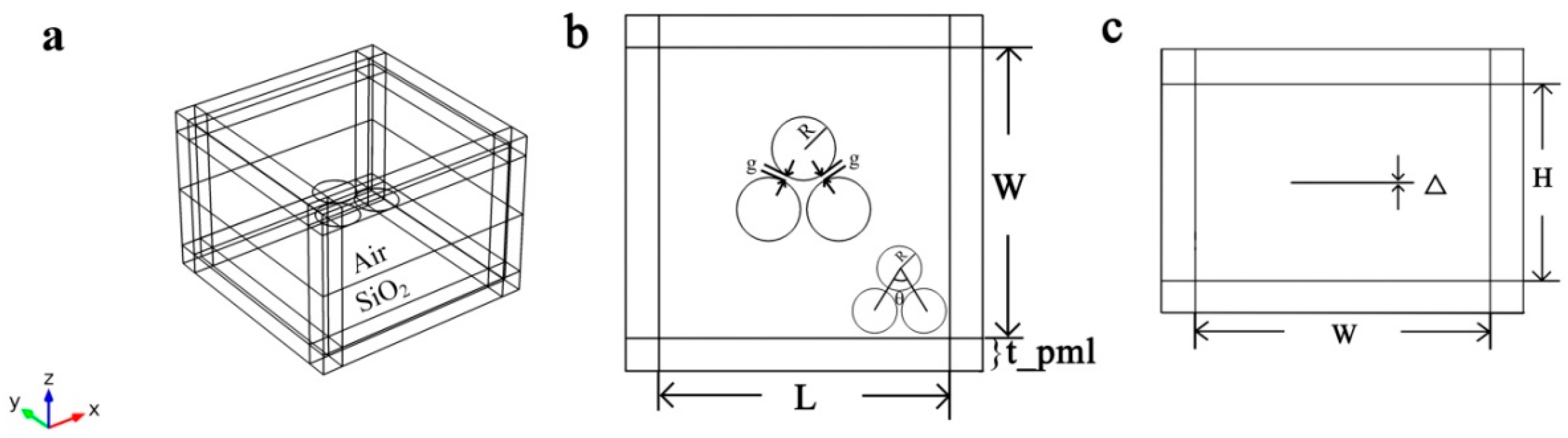
2. Simulation Method and Models

A typical approach to study the optical response of the plasmonic molecule is a semianalytical multiple multipole program [4,12,13] based on boundary discretization. This method was good for understanding the variation of the electromagnetic field with gradient structure modification, and was valid when ka << 1. Spectra of nanoparticle clusters are analyzed based on their structural symmetry using symmetry-adapted linear combinations of the individual nanoparticle plasmon modes [4]. In this paper, we get the full vertical three-dimensional electromagnetic field (E, H) of the nanostructures by calculating the Maxwell’s equations using the finite element method software COMSOL Multiphysics (V5.2, Radio Frequency module, Stockholm, Sweden). Scattering spectra and energy diagrams of the graphene-based trimeric plasmonic molecules are obtained by employing the frequency domain and the eigenfrequency solvers of the commercial software. Then the evolution of the collective mode of the trimer is investigated with the help of irreducible representations of the relevant point group, which is similar to other studies [4,12]. More significantly, the tunable properties of the plasmonic molecule are demonstrated by modifying the chemical potential of the graphene without changing the geometric parameters.
The geometry of the proposed structure is schematically shown in Figure 1a, where three graphene nanodisks are arranged in a triangle and lie on the SiO2 substrate. The nanocluster is illuminated by transverse magnetic (TM) polarization light with electric field E along the longitudinal direction. The extinction cross-section σext, composed of scattering cross-section σsc and absorption-cross section σabs, is expressed as
σ e x t = σ s c + σ a b s ,
with
σ s c = 1 I 0 ( n · S s c ) d S ,
where n indicates the normal vector pointing outwards from the plasmonic molecule, and S s c and I0 are the scattered intensity (Poynting vector) and the incident electromagnetic energy intensity, respectively. The integral is taken over the closed surface of trimer,
σ a b s = 1 I 0 Q d V ,
where Q is the power loss density in the graphene molecule and the integral is taken over the volume.
The graphene nanodisk is treated as a thin film with an equivalent thickness of in our study. Thus, it is characterized by an equivalent permittivity of εg,eq () [40,41], which is a function of both and the surface conductivity of graphene given by εg,eq = −gη0/(k0). Here, η0 (≈377 Ω) is the impedance of air, k0 = 2π/λ represents the wave number of the free space, and σg is the contributions from the interband electron-electron transition σinter and the intraband electron-photon scattering σintra. According to the Kubo formula [34,42,43], graphene’s surface conductivity is written as σ t o t a l = σ i n t e r + σ i n t r a ,
σ i n t e r = i e 2 4 π ln [ 2 | μ c | ( ω i τ 1 ) 2 | μ c | + ( ω i τ 1 ) ] ,
σ i n t r a = i e 2 k B T π 2 ( ω + i τ 1 ) [ μ c k B T + 2 ln ( exp ( μ c k B T ) + 1 ) ] ,
where μc is chemical potential, which is tunable by either chemical doping or external gate voltage. τ is the momentum relaxation time of electrons, and it is set to 0.5 ps throughout this paper. Twenty cores of Xeon CPU and 512 Gb memory were employed to run the calculations. It took 47 h to complete each run.

3. Results and Discussion

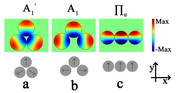
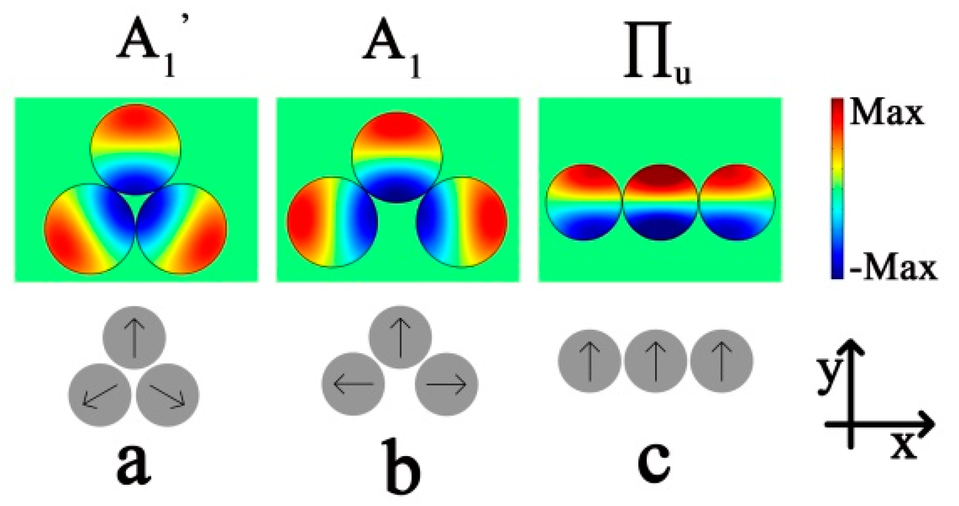
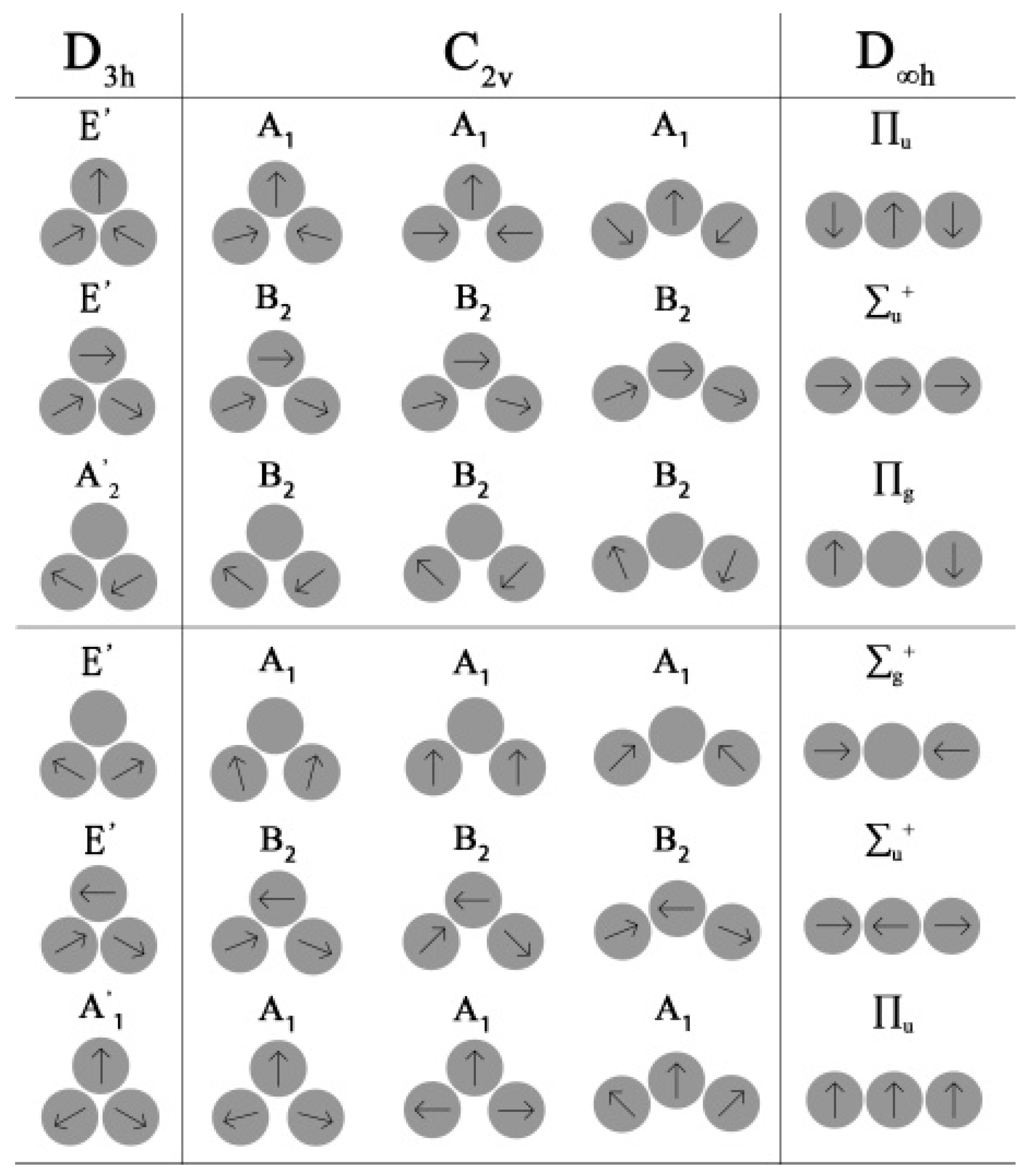
3.1. General Depiction of the Mode of Graphene Plasmonic Trimers

The typical induced surface charge density distributions of graphene plasmonic trimers are depicted in the first row of Figure 2. The direction of the dipole of each “atom” is from negative charge to positive charge, and the corresponding dipole distribution of the whole plasmonic molecule is shown in the second row. The A1’ mode in the first column of the first row belongs to the equilateral triangle (D3h symmetry), which is the highest-symmetry case of a trimeric PM. Here, the direction of the base of the triangle is defined as longitudinal, which in Figure 2 is the x axis. The vertical direction is defined as perpendicular to the base, which in Figure 2 is the y axis. For a succinct expression to describe the distribution of dipole moments, we define the zero net dipole moment along one axis as symmetrical with this axis and the nonzero net dipole moment as asymmetrical. Note that the total moment of the dipole of D3h symmetry is zero due to the symmetry, as shown in the corresponding diagram in the second row of the first column. When the vertex angle of the plasmonic trimer increases, D3h symmetry reduces to C2v symmetry. The total dipole of the whole trimer in the longitudinal direction remains zero, while the counterpart in the vertical direction becomes nonzero, as shown in the second row of Figure 2b. This nonzero momentum suggests that the whole PM is optically active with the polarized light incidents. When the vertex angle becomes 180 ° , the PM turns out to be a linear chain with a symmetrical group of D∞h, where the electromagnetic field demonstrates a ∏u mode, shown in Figure 2c.
In this paper, only the fundamental mode of each plasmonic atom is considered. So we are only concerned about the point dipole located in the center of each plasmonic atom induced by the surface charge. The properties of the quadrupole induced by the surface charge are beyond the scope of this paper. Note that the incident angle of the light does not have a significant effect on either the near field or the far field of the plasmonic molecule; only the in-plane mode field distribution and the scattering spectra with respect to the normal incident electromagnetic field are considered here. Furthermore, the electromagnetic properties of the plasmonic molecule system are computed by solving the classic Maxwell’s equations and the quantum effects, such as electron tunneling between the plasmonic atoms, are ignored, and even the distance between the nanodisks is in nanometer scale.
The trimer plasmonic molecules have six mode categories [2] due to the D3h symmetry, shown in Figure 3. Similar to the molecule orbit, which is composed of linear combinations of each atom, the collective modes of the trimer are made of linear combinations of each plasmonic mode. These six mode categories are divided into two groups, one corresponding to the higher energy of antibonding modes, and the other corresponding to low-energy bonding modes, which is consistent with the plasmon hybridization calculation [1]. In the antibonding group, there are doubly degenerated modes related to the irreducible representation of E’ symmetry. In the highest energy E’ state, the dipoles of the nanodisks on the base show symmetric distribution with respect to the longitudinal direction, so the nonzero net dipole appears along this direction. In the other E’ case, the vertical dipole disappears in the vertex atom of the trimer and the dipoles of the other base atoms arrange symmetrically with respect to the vertical direction. Consequently, it shows the nonzero net dipole along the longitudinal direction. Additionally, there is another nondegenerate mode related to the irreducible representation of A2’ symmetry located at the lower energy state. Interestingly, in this case, the dipole of the vertex atom disappears, similar to the first case of the bonding E’ mode. However, the net dipole of the whole trimer system in antibonding A2’ mode is along the longitudinal direction and in the bonding E’ mode is along the vertical direction. As for the doubly degenerate bonding E’ mode with lower energy, it shows the net dipole along the longitudinal direction. Moreover, among the lower energy state bonding modes, the nondegenerate A1’ is also located at the lowest position, and the dipole of the total plasmonic trimer is centered symmetrically. As a result, the total dipole of the whole plasmonic trimer is zero. As the vertex angle θ increases gradually, the D3h symmetry reduces to lower symmetry C2v, and the plasmonic modes interact with each other, which finally results in lifting the degeneracy of the higher symmetric modes, and new energy states appear, shown in the center columns of Figure 3. The structures of the new plasmonic modes A1 and B2 are gradually changed from those of the D3h modes as the vertex angle θ increases. However, the direction of the dipole moment of the vertex nanodisk does not change when the vertex angle increases, while the counterparts in the other two nanodisks on the base rotate synchronously counterclockwise and clockwise. It is noticeable that for the B2 modes, the nonzero net dipole moment is along the longitudinal direction, while for the A1 mode, the nonzero net dipole moment is along the vertical direction.
When the vertex angle further increases to π, the graphene nanodisks become a chain and the trimer molecule shows D∞h symmetry. The dipole distribution of this symmetry group is illustrated in the right column of Figure 3. The antibonding E’–A1 path evolves to the ∏μ mode, where the dipole moment of the center nanodisk is shown upwards and those of the nanodisks on both the sides show reversed vertical direction. The antibonding E’–B2 path evolves to Σu+ mode, and the net dipole moment is three times of that of the center nanodisk, since all the directions of the three nanodisks are identical along the longitudinal direction. The mode of the antibonding A2’–B2 path becomes ∏g, where the dipole moment of the vertex disks stays at zero and the total is zero. The mode of the bonding E’-A1 path becomes Σg+. The total dipole moment of this mode is also zero, because the dipole of the center nanodisk disappears, and those of the nanodisks on the two sizes are along the reversed longitudinal direction. The bonding E’–B2 path transforms into Σu+ mode and the mode evolution of bonding Σu+ irreducible representation of the D∞h symmetry group, where the dipole of the center nanodisk points left, while the other two nanodisks in the two sides point right. The mode evolution of bonding A1’–A1 path transfers to ∏u irreducible presentation of the D∞h symmetry group, and the net dipole of the plasmonic molecule is three times of that of the center nanodisk upwards along the vertical direction. The nonzero net dipole moment of the plasmonic molecule with specific direction suggests selective optical sensitivity with different impinging linearly polarized electromagnetic waves.

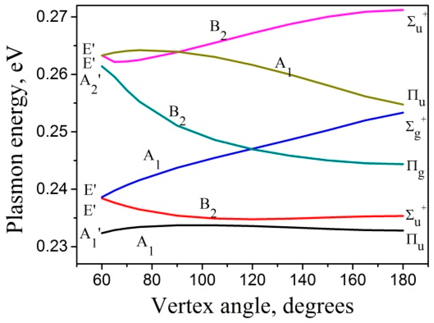
3.2. Energy Diagram of the Plasmonic Trimer

The energy diagram of the plasmon as a function of vertex angle θ is shown in Figure 4. The plasmonic energy is given by ћω, where ћ is the reduced Planck constant. It should be pointed out that the energy of the doubly degenerated E’ modes splits into two lines as θ increases in both antibonding and bonding groups. In the antibonding group, the mode evolution trenches of the lifted degenerated modes are almost opposite to each other. The antibonding E’–B2 mode shows first a slightly red shift and then a blue shift, while the antibonding E’–A1 mode demonstrates a slightly blue shift and then a red shift at high vertex angles. The energy of the two modes is approximately equal when θ is 90°. As θ further increases to 180°, the antibonding E’–B2 mode transfers to the Σu+ mode, which is asymmetric with the longitudinal direction and symmetric with the vertical direction, and the path of the E’–B2–Σu+ mode evolution is formed. The antibonding E’–A1 mode reaches the Πu mode, which is symmetric with the x axis and asymmetric with the y axis, and the path of the E’–A1–Πu mode evolution is set up. The antibonding A2’–B2 mode evolution path red shifts monotonously and reaches Πg mode. In the bonding group, the doubly degenerated E’ mode is lifted as the vertex angle increases. However, unlike the antibonding group, the bonding E’–A1 mode shows monotonously blue shift and finally reaches the Σg+ mode, where the optical field distribution is symmetric with both longitudinal and vertical directions when the vertex angle reaches 180°. Interestingly, the energy of the plasmon of the bonding E’–A1 path surpasses that of the antibonding A2’–B2 path when the vertex angle is higher than 120°. On the other hand, the bonding E’–B2 mode shows monotonous red shift and finally reaches the Σu+ mode. The lowest mode evolution path bonding A1’–A1 remains stable. In general, the vertex evolution of the scattering extinction cross-section in energy state throughout the range of the vertex angle was studied. Eventually, it turns to the Πu mode, which is symmetric in the longitudinal direction and asymmetric in the vertical direction. The spectra are consistent with the energy diagrams shown in Figure 4.

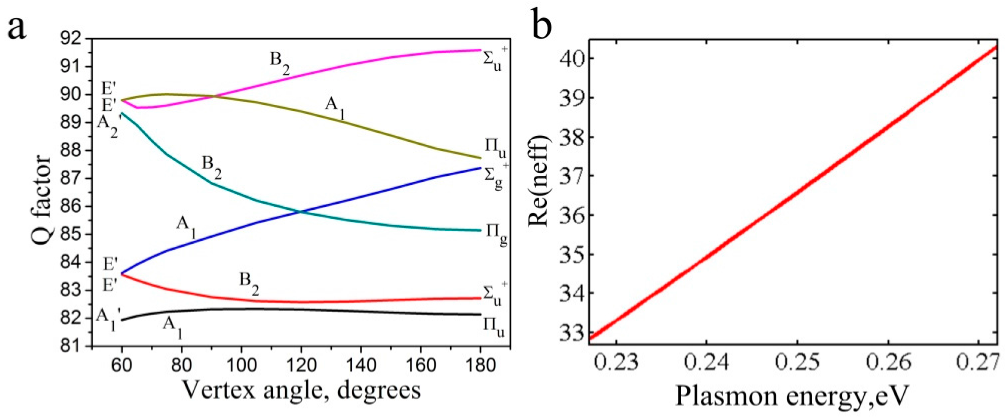
3.3. Quality Factor of Graphene Plasmonic Trimers

The quality factor (Q factor) of graphene plasmonic trimers is calculated as a function of the vertex angle (θ), shown in Figure 5. It can be seen that the figures of the Q factor are identical to those of the energy states. In general, the Q factor relies on both the confinement and loss of the plasmon. As we know, total loss of graphene is composed of two parts, radiation loss and absorption loss; therefore, the Q factor can be written as 1/Q = 1/Qabs + 1/Qrad [44]. Within the frequency range of interest in this work, when the plasmon energy increases, the confinement capability of graphene is enhanced, so the radiation loss decreases, while the Qrad increases. The quality factor of absorption can be defined as 1/Qabs = γ(β)/(2|i(β)|), where γ(β) and |i(β)| are the real part and the imaginary part of the propagation constant of the SPP mode, respectively. The real part of the propagation constant γ(β) is expressed as k0neff, where neff represents the effective mode index of SPPs, indicating the confinement ability of graphene, while the imaginary part of the propagation constant indicates the loss of SPPs. The effective mode index (neff) as a function of plasmon energy with a range from 0.225 to 0.272 eV is shown in Figure 5b. Therefore, the Q factor increases linearly with the plasmon energy.

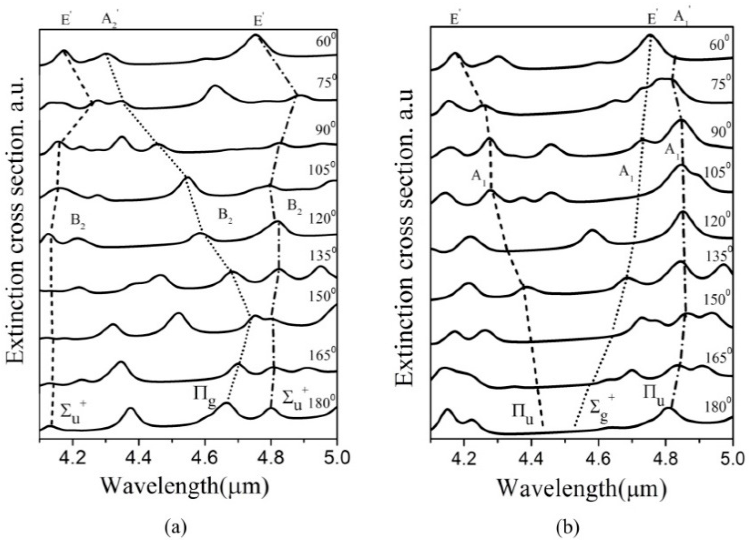
3.4. Scattering Properties of Graphene Plasmonic Trimers

As was pointed out above, the nonzero net dipole moment of the graphene plasmonic trimer system enables optical sensitivity with specific polarization. The A1 modes show a nonzero net dipole moment along the vertical direction, while the B2 modes demonstrate a nonzero net dipole moment along the longitudinal direction. The far field scattering extinction cross-section as a function of wavelength (from 4.1 μm to 5.0 μm) with different vertex angles θ is shown in Figure 6. The scattering characteristics of graphene plasmonic trimers shown in Figure 6 are generally consistent with the plasmon energy diagrams shown in Figure 4. The evolution of the peak positions of the scattering cross-section spectra comes from the net nonzero dipole moments of the graphene trimer as a function of vertex angle. The change of net dipole moments of graphene trimers with increased vertex angle θ gives rise to the perturbation in extinction spectra. We chose the E’–A1–Σg+ and A1’–A1–Πu mode evolution paths with vertical polarization for further exploration of transformation mechanisms in extinction spectra. With θ = 60 ° , the net dipole moments of the graphene trimer are relatively large in E’ mode (Figure 2), where the mode is bright and the peak in extinction spectra is also obvious (Figure 6). As θ becomes larger than 60 ° , E’ mode transforms to A1 mode with a decrease of net dipole moment due to the rotation of the dipole moment in two base nanodisks, which gives rise to a reduction of the peak in extinction spectra. When θ = 180 ° , A1 mode transforms into a dark Σg+ mode with zero net dipole moment, and the peak completely vanishes in extinction spectra. On the contrary, the A1’–A1–Πu mode evolution path shows a transition that a dark A1’ mode transforms into a bright Πu mode with an increase of net dipole moment of graphene trimers. Consequently, a new peak appears and the corresponding peaks in extinction spectra gradually become more distinguishable. Note that there are some peaks that are not related to any mode evolution paths discussed here. These might belong to the higher order modes or the hybridized modes, which will be examined in further exploration.

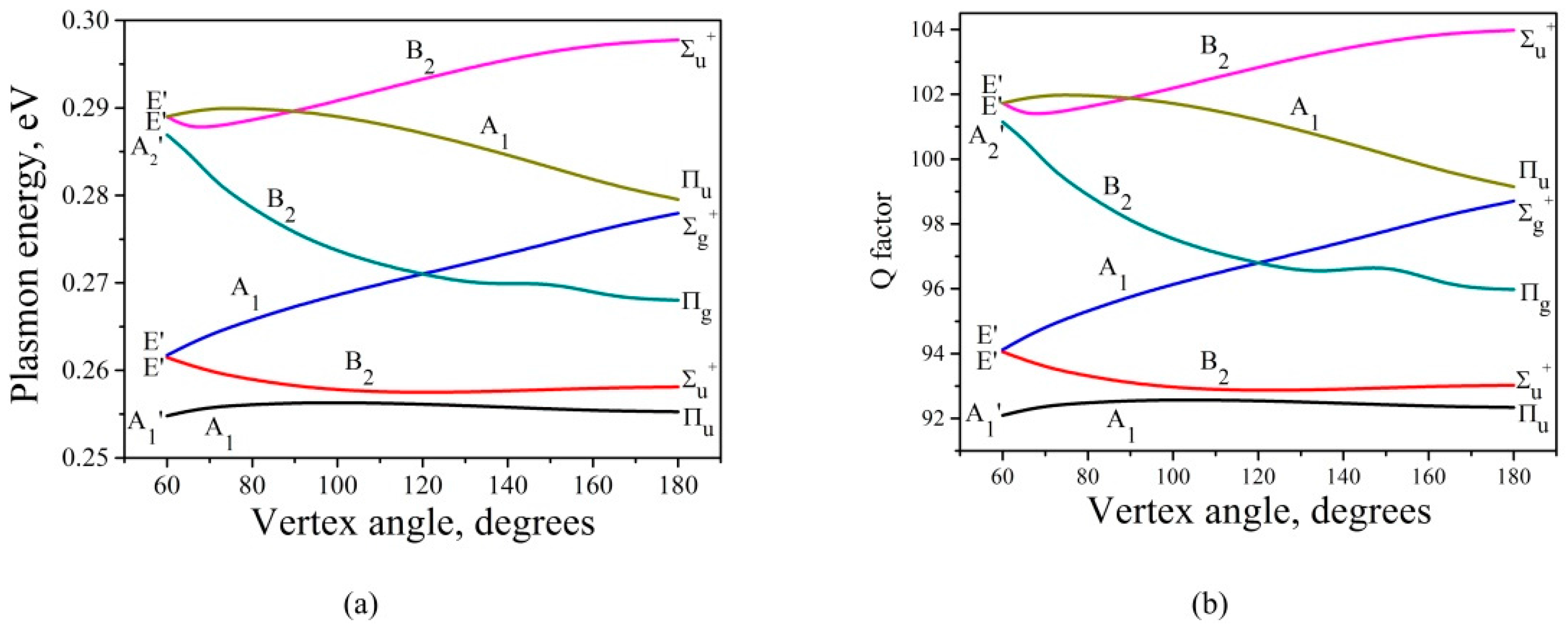
3.5. Frequency Tunability of Graphene Plasmonic Trimers

To demonstrate the tunable advantage of graphene, we keep the identical geometry of the graphene trimer and change the chemical potential to 0.6 eV. The calculated resonance energy diagram and the corresponding scattering spectra are plotted in Figure 7 and Figure 8. It is seen that the general trend is that the energy diagram and the scattering spectra are identical with those of graphene trimer with a chemical potential of 0.5 eV. The difference is the blue-shift effect in the corresponding spectra and the energy diagrams. This comes from the higher frequency of the eigenmodes of the trimer with a higher chemical potential. Also, the corresponding quality factors are higher due to the lower absorption loss. This property enables the graphene trimer to be flexibly used in a wide spectral range by changing the chemical potential of graphene. This structure will benefit development of multiband graphene nanosensors. It should be noted that the refractive index of the SiO2 affects the positions of the plasmonic peaks of the scattering spectra. However, it does not influence the mechanism of mode evolution and frequency tunability.

3.6. Fabrication Process Suggestion

In terms of the fabrication process of graphene plasmonic trimers, the graphene monolayer with certain chemical potential, i.e., doping concentration, could be transferred to the SiO2 substrate. It could also be deposited on the SiO2 substrate by the chemical vapor deposition technique. Then negative tone electron beam resist is spin-coated on the graphene, followed by the exposure process. Later, the designed patterns are transferred to negative tone electron beam resist after development. As for the periodic patterns, the distance between the neighboring trimers should be far enough to avoid mode coupling between the trimers. Then the patterns are transferred to the graphene monolayer by the reactive ion etching technique, using the electron beam resist as the etching mask. Finally, the remaining resist is totally removed by rinsing the wafer with solvent, and the samples are ready for testing.

4. Summary

In this work, following the works of Chuntonov and Haran [4,12,13] and exploiting their ideas, we propose plasmonic trimer composed of graphene nanodisk with a more compact footprint than the conventional metals. The effect of symmetry of the graphene cluster’s electromagnetic properties is numerically investigated by gradually increasing the vertex angle. With increased vertex angle, the symmetry of the plasmonic molecule breaks, and the degenerate plasmonic mode lifts. Consequently, the clusters demonstrate nonzero net dipole moments, which further show optical sensitivity to the specific linear polarization light in the mid-infrared region. The calculated vertex angle–dependent extinction cross-section spectra agree well with the plasmonic energy diagrams. Furthermore, the frequency tunability of the graphene nanostructure is examined by varying the chemical potential without changing the geometry of the proposed structures, which is impossible with the conventional metals. Blue shift of the plasmonic resonant modes is observed with a high chemical potential. The proposed graphene plasmonic trimers could play a significant role in enhancing the performance of optical components based on single whispering-gallery mode nanocavity, such as directional emission nanocavity lasers and high-sensitivity sensors.

Acknowledgments

The authors are grateful for support from the Natural Science Fund of China under grant nos. 11774103, 61378058, and 61575070, Fujian Province Science Funds for Distinguished Young Scholar (no. 2015J06015), and the Promotion Program for Young and Middle-Aged Teachers in Science and Technology Research of Huaqiao University (no. ZQN-YX203).

Author Contributions

Weibin Qiu provided the original idea of this project; Houbo Chen, Pingping Qiu, and Junbo Ren did the simulations; Weibin Qiu, Houbo Chen, Pingping Qiu, Zhili Lin, Junbo Ren, Jiaxian Wang, Qiang Kan, and Jiaoqing Pan analyzed the data; Weibin Qiu, Junbo Ren, and Houbo Chen wrote the paper.

Conflicts of Interest

The authors claim no conflicts of interest regarding this work.

References

  1. Ku, J.F.; Chen, Q.D.; Ma, X.W.; Yang, Y.D.; Huang, Y.Z.; Xu, H.L.; Sun, H.B. Photonic-molecule single-mode laser. IEEE Photonics Technol. Lett. 2015, 27, 1157–1160. [Google Scholar] [CrossRef]
  2. Kudryashov, A.V.; Boriskina, S.V.; Paxton, A.H.; Benson, T.M.; Sewell, P.; Ilchenko, V.S. Photonic molecules made of matched and mismatched microcavities: New functionalities of microlasers and optoelectronic components. Proc. SPIE 2007, 6452, 64520X. [Google Scholar] [CrossRef]
  3. Vahala, K.J. Optical microcavities. Nature 2003, 424, 839–846. [Google Scholar] [CrossRef] [PubMed]
  4. Chuntonov, L.; Haran, G. Trimeric plasmonic molecules: The role of symmetry. Nano Lett. 2011, 11, 2440–2445. [Google Scholar] [CrossRef] [PubMed]
  5. Wang, H.; Brandl, D.W.; Nordlander, P.; Halas, N.J. Plasmonic nanostructures  artificial molecules. Acc. Chem. Res. 2007, 40, 53–62. [Google Scholar] [CrossRef] [PubMed]
  6. Mukherjee, S.; Sobhani, H.; Lassiter, J.B.; Bardhan, R.; Nordlander, P.; Halas, N.J. Fanoshells: Nanoparticles with built-in fano resonances. Nano Lett. 2010, 10, 2694–2701. [Google Scholar] [CrossRef] [PubMed]
  7. Luk’yanchuk, B.; Zheludev, N.I.; Maier, S.A.; Halas, N.J.; Nordlander, P.; Giessen, H.; Chong, C.T. The Fano resonance in plasmonic nanostructures and metamaterials. Nat. Mater. 2010, 9, 707–715. [Google Scholar] [CrossRef] [PubMed]
  8. Hentschel, M.; Saliba, M.; Vogelgesang, R.; Giessen, H.; Alivisatos, A.P.; Liu, N. Transition from isolated to collective modes in plasmonic oligomers. Nano Lett. 2010, 10, 2721–2726. [Google Scholar] [CrossRef] [PubMed]
  9. Papasimakis, N.; Fedotov, V.A.; Zheludev, N.I.; Prosvirnin, S.L. Metamaterial analog of electromagnetically induced transparency. Phys. Rev. Lett. 2008, 101, 253903. [Google Scholar] [CrossRef] [PubMed]
  10. Liu, N.; Langguth, L.; Weiss, T.; Kastel, J.; Fleischhauer, M.; Pfau, T.; Giessen, H. Plasmonic analogue of electromagnetically induced transparency at the drude damping limit. Nat. Mater. 2009, 8, 758–762. [Google Scholar] [CrossRef] [PubMed]
  11. Willets, K.A.; Van Duyne, R.P. Localized surface plasmon resonance spectroscopy and sensing. Annu. Rev. Phys. Chem. 2007, 58, 267–297. [Google Scholar] [CrossRef] [PubMed]
  12. Chuntonov, L.; Haran, G. Optical activity in single-molecule surface-enhanced raman scattering: Role of symmetry. MRS Bull. 2013, 38, 642–647. [Google Scholar] [CrossRef]
  13. Chuntonov, L.; Haran, G. Effect of symmetry breaking on the mode structure of trimeric plasmonic molecules. J. Phys. Chem. C 2011, 115, 19488–19495. [Google Scholar] [CrossRef]
  14. Verre, R.; Yang, Z.J.; Shegai, T.; Kall, M. Optical magnetism and plasmonic Fano resonances in metal-insulator-metal oligomers. Nano Lett. 2015, 15, 1952–1958. [Google Scholar] [CrossRef] [PubMed]
  15. Fan, J.A.; Wu, C.; Bao, K.; Bao, J.; Bardhan, R.; Halas, N.J.; Manoharan, V.N.; Nordlander, P.; Shvets, G.; Capasso, F. Self-assembled plasmonic nanoparticle clusters. Science 2010, 328, 1135–1138. [Google Scholar] [CrossRef] [PubMed]
  16. Zhao, J.; Qiu, W.; Huang, Y.; Wang, J.X.; Kan, Q.; Pan, J.Q. Investigation of plasmonic whispering-gallery mode characteristics for graphene monolayer coated dielectric nanodisks. Opt. Lett. 2014, 39, 5527–5530. [Google Scholar] [CrossRef] [PubMed]
  17. Qiu, W.; Liu, X.; Zhao, J.; He, S.; Ma, Y.; Wang, J.-X.; Pan, J. Nanofocusing of mid-infrared electromagnetic waves on graphene monolayer. Appl. Phys. Lett. 2014, 104, 041109. [Google Scholar] [CrossRef]
  18. Zhang, H.; Virally, S.; Bao, Q.; Ping, L.; Massar, S.; Godbout, N.; Kockaert, P. Z-scan measurement of the nonlinear refractive. Opt. Lett. 2012, 37, 1856–1858. [Google Scholar] [CrossRef] [PubMed]
  19. Li, Z.Q.; Henriksen, E.A.; Jiang, Z.; Hao, Z.; Martin, M.C.; Kim, P.; Stormer, H.L.; Basov, D.N. Dirac charge dynamics in graphene by infrared spectroscopy. Nat. Phys. 2008, 4, 532–535. [Google Scholar] [CrossRef]
  20. Novoselov, K.S.; Geim, A.K.; Morozov, S.V.; Jiang, D.; Katsnelson, M.I.; Grigorieva, I.V.; Dubonos, S.V.; Firsov, A.A. Two-dimensional gas of massless Dirac fermions in graphene. Nature 2005, 438, 197–200. [Google Scholar] [CrossRef] [PubMed] [Green Version]
  21. Ren, J.; Qiu, W.; Chen, H.; Qiu, P.; Lin, Z.; Wang, J.X.; Kan, Q.; Pan, J.Q. Electromagnetic field coupling characteristics in graphene plasmonic oligomers: From isolated to collective modes. Phys. Chem. Chem. Phys. 2017, 19, 14671–14679. [Google Scholar] [CrossRef] [PubMed]
  22. Hwang, E.H.; Das Sarma, S. Dielectric function, screening, and plasmons in two-dimensional graphene. Phys. Rev. B 2007, 75, 205418. [Google Scholar] [CrossRef]
  23. Liu, M.; Yin, X.; Ulin-Avila, E.; Geng, B.; Zentgraf, T.; Ju, L.; Wang, F.; Zhang, X. A graphene-based broadband optical modulator. Nature 2011, 474, 64–67. [Google Scholar] [CrossRef] [PubMed]
  24. Mittendorff, M.; Li, S.S.; Murphy, T.E. Graphene-based waveguide-integrated terahertz modulator. ACS Photonics 2017, 4, 316–321. [Google Scholar] [CrossRef]
  25. Correas-Serrano, D.; Gomez-Diaz, J.S.; Alu, A.; Melcon, A.A. Electrically and magnetically biased graphene-based cylindrical waveguides: Analysis and applications as reconfigurable antennas. IEEE Trans. Terahertz Sci. Technol. 2015, 5, 951–960. [Google Scholar] [CrossRef]
  26. Sensale-Rodriguez, B.; Yan, R.; Zhu, M.; Jena, D.; Liu, L.; Grace Xing, H. Efficient terahertz electro-absorption modulation employing graphene plasmonic structures. Appl. Phys. Lett. 2012, 101, 261115. [Google Scholar] [CrossRef]
  27. Qiu, P.; Qiu, W.; Lin, Z.; Chen, H.; Tang, Y.; Wang, J.X.; Kan, Q.; Pan, J.Q. Investigation of the band structure of graphene-based plasmonic photonic crystals. Nanomaterials 2016, 6, 166. [Google Scholar] [CrossRef] [PubMed]
  28. Hanson, G.W. Dyadic green’s functions and guided surface waves for a surface conductivity model of graphene. J. Appl. Phys. 2008, 103, 064302. [Google Scholar] [CrossRef]
  29. Amanatiadis, S.A.; Kantartzis, N.V.; Tsiboukis, T.D. A loss-controllable absorbing boundary condition for surface plasmon polaritons propagating onto graphene. IEEE Trans. Magn. 2015, 51, 4. [Google Scholar] [CrossRef]
  30. Papadimopoulos, A.N.; Amanatiadis, S.A.; Kantartzis, N.V.; Rekanos, I.T.; Zygiridis, T.T.; Tsiboukis, T.D. A convolutional PML scheme for the efficient modeling of graphene structures through the ADE-FDTD technique. IEEE Trans. Magn. 2017, 53, 1–4. [Google Scholar] [CrossRef]
  31. Zhao, J.; Liu, X.; Qiu, W.; Ma, Y.; Huang, Y.; Wang, J.X.; Qiang, K.; Pan, J.Q. Surface-plasmon-polariton whispering-gallery mode analysis of the graphene monolayer coated ingaas nanowire cavity. Opt. Express 2014, 22, 5754–5761. [Google Scholar] [CrossRef] [PubMed]
  32. Chen, J.; Badioli, M.; Alonso-Gonzalez, P.; Thongrattanasiri, S.; Huth, F.; Osmond, J.; Spasenovic, M.; Centeno, A.; Pesquera, A.; Godignon, P.; et al. Optical nano-imaging of gate-tunable graphene plasmons. Nature 2012, 487, 77–81. [Google Scholar] [CrossRef] [PubMed]
  33. Kim, M.W.; Ku, P.C. Lasing in a metal-clad microring resonator. Appl. Phys. Lett. 2011, 98, 131107. [Google Scholar] [CrossRef]
  34. Ju, L.; Geng, B.; Horng, J.; Girit, C.; Martin, M.; Hao, Z.; Bechtel, H.A.; Liang, X.; Zettl, A.; Shen, Y.R.; et al. Graphene plasmonics for tunable terahertz metamaterials. Nat. Nanotechnol. 2011, 6, 630–634. [Google Scholar] [CrossRef] [PubMed]
  35. Ren, J.B.; Wang, G.Q.; Qiu, W.B.; Lin, Z.L.; Chen, H.B.; Qiu, P.P.; Wang, J.X.; Kan, Q.; Pan, J.Q. Optimization of the Fano resonance lineshape based on graphene plasmonic hexamer in mid-infrared frequencies. Nanomaterials 2017, 7, 238. [Google Scholar] [CrossRef] [PubMed]
  36. Amanatiadis, S.; Kantartzis, N. Distortion of surface plasmon polariton propagation on graphene due to chemical potential variation. Appl. Phys. A 2016, 122, 313. [Google Scholar] [CrossRef]
  37. Low, T.; Avouris, P. Graphene plasmonics for terahertz to mid-infrared applications. ACS Nano 2014, 8, 1086–1101. [Google Scholar] [CrossRef] [PubMed]
  38. Chen, H.B.; Qiu, W.B.; Qiu, P.P.; Ren, J.B.; Lin, Z.L.; Wang, J.X.; Kan, Q.; Pan, J.Q. Mode coupling properties of the plasmonic dimers composed of graphene nanodisks. Appl. Sci. 2017, 7, 359. [Google Scholar] [CrossRef]
  39. Qiu, W.; Huang, Y.; Chen, H.; Qiu, P.; Tang, Y.; Wang, J.-X.; Kan, Q.; Pan, J.-Q. Coupling of whispering-gallery modes in the graphene nanodisk plasmonic dimers. Plasmonics 2016, 12, 39–45. [Google Scholar] [CrossRef]
  40. Lu, W.B.; Zhu, W.; Xu, H.J.; Ni, Z.H.; Dong, Z.G.; Cui, T.J. Flexible transformation plasmonics using graphene. Opt. Express 2013, 21, 10475–10482. [Google Scholar] [CrossRef] [PubMed]
  41. Vakil, A.; Engheta, N. Transformation optics using graphene. Science 2011, 332, 1291–1294. [Google Scholar] [CrossRef] [PubMed]
  42. Wang, B.; Zhang, X.; Yuan, X.C.; Teng, J.H. Optical coupling of surface plasmons between graphene sheets. Appl. Phys. Lett. 2012, 100, 4. [Google Scholar] [CrossRef]
  43. Gusynin, V.P.; Sharapov, S.G.; Carbotte, J.P. Magneto-optical conductivity in graphene. J. Phys. Condens. Matter 2007, 19, 25. [Google Scholar] [CrossRef]
  44. Huang, Y.; Qiu, W.; Lin, S.; Zhao, J.; Chen, H.; Wang, J.-X.; Kan, Q.; Pan, J.-Q. Investigation of plasmonic whispering gallery modes of graphene equilateral triangle nanocavities. Sci. China Inf. Sci. 2016, 59, 042413. [Google Scholar] [CrossRef]
Figure 1. (a) Three-dimensional geometry of the proposed structure: (b) vertical view, (c) left view. Here, the radius (R), height (), and chemical potential (μc) of graphene are 50 nm, 0.335 nm, and 0.5 eV, respectively. θ is the vertex angle of trimeric plasmonic molecules (PMs), shown in the inset of (b), and g = 1 nm is the distance between the individual plasmonic “atoms.” Outside the graphene is the free space, where the length (L), width (W), and height (H) of the computation window are 450 nm, 450 nm, and 300 nm, respectively.
Applsci 08 00374 g001
Figure 2. Surface charge density distributions of typical trimeric graphene plasmonic trimers.
Applsci 08 00374 g002
Figure 3. Dipole distributions of graphene plasmonic trimers: equilateral triangle (D3h symmetry) modes (left column), isosceles triangle (C2v symmetry) modes (center columns), and linear chain (D∞h symmetry) modes (right column).
Applsci 08 00374 g003
Figure 4. Plasmon energy diagram of trimeric graphene molecules with various vertex angles.
Applsci 08 00374 g004
Figure 5. (a) Quality factor (Q factor) as a function of the the vertex angle (θ), (b) the real part of effective refractive index as a function of the plasmon energy.
Applsci 08 00374 g005
Figure 6. Scattering extinction cross-section as a function of wavelength ranging from 4.5 to 5.5 μm. (a) The incident light is longitudinally polarized, (b) the incident light is vertically polarized.
Applsci 08 00374 g006
Figure 7. (a) Plasmonic energy diagram of graphene plasmonic trimers. (b) Corresponding quality factors of the plasmon modes as a function of vertex angle. The chemical potential of graphene is 0.6 eV. Compared with trimers of 0.5 eV graphene, the energy diagram shows blue shift, and the corresponding Q factors increase.
Applsci 08 00374 g007
Figure 8. Extinction cross-section spectra of graphene trimers with 0.6 eV chemical potential under linearly polarized mid-infrared light. (a) B2 modes that are optically active with longitudinal polarization, (b) A1 modes that are optically active with vertical polarization. Compared with those of 0.5 eV graphene, the corresponding peaks in the spectra show blue shift.
Applsci 08 00374 g008

