1. Introduction
Phase-contrast imaging methods have attracted a lot of attention in the scientific community due to their ability to offer enhanced information on the inner structure of the various objects, in addition to conventional attenuation contrast [
1,
2]. These methods enable the detection of X-ray refraction and scattering while passing through the object under investigation. Following increasing interest, the application of phase-contrast imaging was made available not only at synchrotron facilities with highly coherent and monochromatic radiation, but also with conventional X-ray tubes [
1]. X-ray refraction and scattering within laboratory setups are usually detected with the help of the intended optical components, so-called gratings, introduced into the beam path. Several interferometric [
2,
3,
4] and non-interferometric [
5,
6,
7] techniques utilizing grating structures have been proposed.
Despite the remarkable results in imaging achieved by these techniques, there is still an open question as to whether it is possible to further optimize the stability of the setup, acquisition time, and flux efficiency [
8]. From this perspective, one of the most promising approaches is the utilization of a single optical element in a single-shot configuration. The implementation of only one optical component in the beam path relaxes the alignment requirements, increases the mechanical stability and versatility of the setup, and significantly reduces the attenuation introduced by the grating. Single-shot acquisition of imaging information, in turn, substantially shortens the total exposure time, simplifies the experimental procedure and reduces the total amount of data to be processed. All those advantages can be exploited by non-interferometric single-exposure imaging methods [
9,
10,
11], in which all three contrast modalities are retrieved from a single projection image. In this approach, the incident beam is periodically modulated by the absorption grating, which can be placed before or after the object. The projected grating pattern distortion introduced by the object is recorded with a single exposure and then analyzed [
6,
9,
10,
11,
12,
13,
14,
15].
To respond to the growing interest in the single-shot phase-contrast imaging, one should pay special attention to the optical components in use. Gratings for X-ray imaging are represented by a matrix with periodically-alternating opaque and transparent structures. When X-ray radiation is incident on the grating, it is partially transmitted by the low-absorbing substrate, while radiation incident on the gold structures’ array is predominantly absorbed. Diffraction on the multiple apertures occurs, but its effect is feeble due to the short wavelength of X-rays. The grating converts X-ray tube radiation into multiple coherent sources; the wavefront is sampled to create a pattern inverse to the grating design. One-dimensional line gratings conventionally used in phase-contrast imaging allow only orientation-dependent analysis of structures, because only sensitivity in the direction, perpendicular to the grating lamellae, is possible [
16]. Providing enhanced information on the material structure in several directions of two-dimensional gratings has been introduced [
9,
12,
13,
14,
16].
As in the single-shot phase-contrast imaging, the information is retrieved from the overlapped grating-object image, it is of great importance to ensure high quality and efficient performance of the grating. The sensitivity of the discussed single-shot imaging method scales with the period of the grating [
9]. In order to sufficiently resolve the grating pattern, the camera pixel size should be equal to, or less than, one-third of the projected grating period [
17]. This means that the detector’s resolution sets the lower limit for the grating period. To achieve the highest possible resolution within a specific setup, the use of customized gratings is superior to the off-the-shelf grids. As it was reported previously [
12], the gratings with greater symmetry may increase the efficiency of the wavefront sampling. A higher degree of periodicity of the grating structures improves the quality of the final image, thus, it is necessary to remove, or at least reduce to the minimum, the number of irregularities in the grating pattern. Another point to draw attention to is the profile of the grating structures. Due to the limitations imposed by the fabrication technique in use, usually, it is not a rectangular function. A possible slope of the grating sidewalls can introduce different absorption levels resulting in a blurring of the image, additional to the blurring by the X-ray tube focal spot size and point spread function of the camera. Thus, the improvement of gratings periodicity and shape can enhance the quality of the final image and possibly diminish the requirements on the X-ray tube and camera.
To evaluate the performance of the two-dimensional grating at the specific X-ray energy, one needs to study the wavefront sampling induced by it. The efficiency of wavefront modulation is a characteristic that directly influences the contrast of the image acquired by the detector. Here, by the efficiency of wavefront modulation (WFM), we mean the intensity variation between opaque and transparent grating areas as recorded by the camera. This can be expressed similarly to the visibility characteristic used in the interferometric methods [
18]:
where
It is the intensity, transmitted by the transparent structure, and
Iop is the intensity, transmitted by the opaque structure. It is important to note that the values of
It and
Iop vary significantly with X-ray energy, and the same grating will perform differently at the different radiation energy. Moreover, as conventional sources, such as X-ray tubes, are not monochromatic and emit energy in a certain spectrum, the ideal case of WFM = 1 is not possible to attain in reality. Single-shot X-ray imaging has been demonstrated even with WFM < 0.5 [
4,
15]; however, increasing the efficiency of wavefront sampling can enhance the quality of the final image. WFM, being of relative value, can serve as a benchmarking measure for a particular grating to be used in a setup with the defined source and detector. To explore the possibilities of the single-shot imaging approach, one should achieve the highest wavefront modulation, keeping a high degree of periodicity for the gratings in use. In this regard, the objective of this work is to develop high-quality gratings of various periods to be used for customized materials science and medical applications at energies up to 25 keV.
2. Materials and Methods
UV lithography is one of the most available and widely-used microstructure fabrication techniques for patterning of periodic structures over a large area. It can provide gratings with high quality if the technological process is optimized for the required structure size regarding the diffraction limit of the resolution [
19]. Each step of the manufacturing process requires optimization to eliminate the distortions of the predetermined pattern due to various phenomena, but greater attention must be paid to the fine-tuning of the exposure dose, which is directly related to the number of cross-linking reactions occurring in the photopolymer (photoresist) layer. Cross-linked areas form an intended pattern shape, which is subsequently used to serve as a mask for electroforming. Properties of the pattern, such as mechanical stability, homogeneity, and uniformity of the design (height and periodicity), directly depend on the photoresist performance during and after exposure. In the case of the negative photoresist, the exposure dose should be high enough to generate the cross-linking along the photoresist depth sufficient to adhere it to the substrate carrier and to avoid structure deflection followed by the pattern collapse due to insufficient stiffness. Overexposure, in turn, can result in significant distortion of the pattern shape due to diffusion of the photoactive components. Furthermore, overexposure can lead to cracking of the cross-linked areas due to photoresist shrinkage. The optimization of exposure dose requires a characterization of photoresist response to irradiation, which can be done by photoresist sensitivity curves.
2.1. Sensitivity Curve for Negative Epoxy-Based Photoresist
To determine the proper exposure parameters, we used sensitivity (contrast) curve procedure, which is used to assess the lithographic performance of photoresist [
18]. A set of samples was prepared to carry out sensitivity curve procedure to determine the proper exposure parameters. A thin (few nm) layer of hexamethyldisilazane was deposited on silicon wafers with a thickness of 525 µm during substrate pretreating with heating up to 150 °C for 30 min to increase the adhesion of the photoresist to the wafer. Using different regimes to achieve layer thicknesses of 10 µm, 15 µm, and 20 µm, the epoxy-based negative mr-X 10 photoresist (micro resist technology GmbH, Berlin, Germany) was spin-coated on the wafers. Thicknesses higher than 20 µm were not used for the sensitivity curve procedure, as in this case the dose is not uniformly distributed along the photoresist thickness due to absorption; the ratio of the bottom and top dose is not close to unity, which violates the basic assumption of the approach [
18].
The soft bake was performed using a hot plate at the temperature of 95 °C for 10 min. Exposure was carried out with a mercury UV lamp. The stability and distribution of the total incident radiation power were controlled by Karl Suss UV intensity meter model 1000. The intensity value was 15 mW/cm2 with 1 mW/cm2 deviation from the center to the edge, the measurements were performed for the i-line of the mercury spectrum (λ = 365 nm). The exposure was done using double-mask geometry: the lower mask was a Cr-quartz mask with alternating dark and light tone regions with a pattern of structure sizes from two up to 50 µm; the upper mask was a slit that allowed dividing the exposure area into 15 sectors that received a different dose with a constant step. The dose was tuned within a determined range by changing the exposure time. The exposure was carried out using vacuum contact alignment to eliminate diffraction effects: the wafer and the mask were placed in the vacuum chamber to ensure the absence of a gap between the mask and the photoresist layer.
The exposed samples were subjected to post exposure bake (PEB) in the oven for four hours with temperature changing from 70 °C to 90 °C and subsequent cooling to room temperature. A wet development of the exposed photoresist layers was carried out in propylene glycol monomethyl ether acetate in order to dissolve the unexposed area of mr-X 10 photoresist layers, and then the samples were rinsed in isopropanol alcohol. After development, the samples were air dried in a convection oven at 30 °C and then the height of the formed micropattern was measured with a Tencor P-2 long scan profiler with an instrumental accuracy of 25 Å.
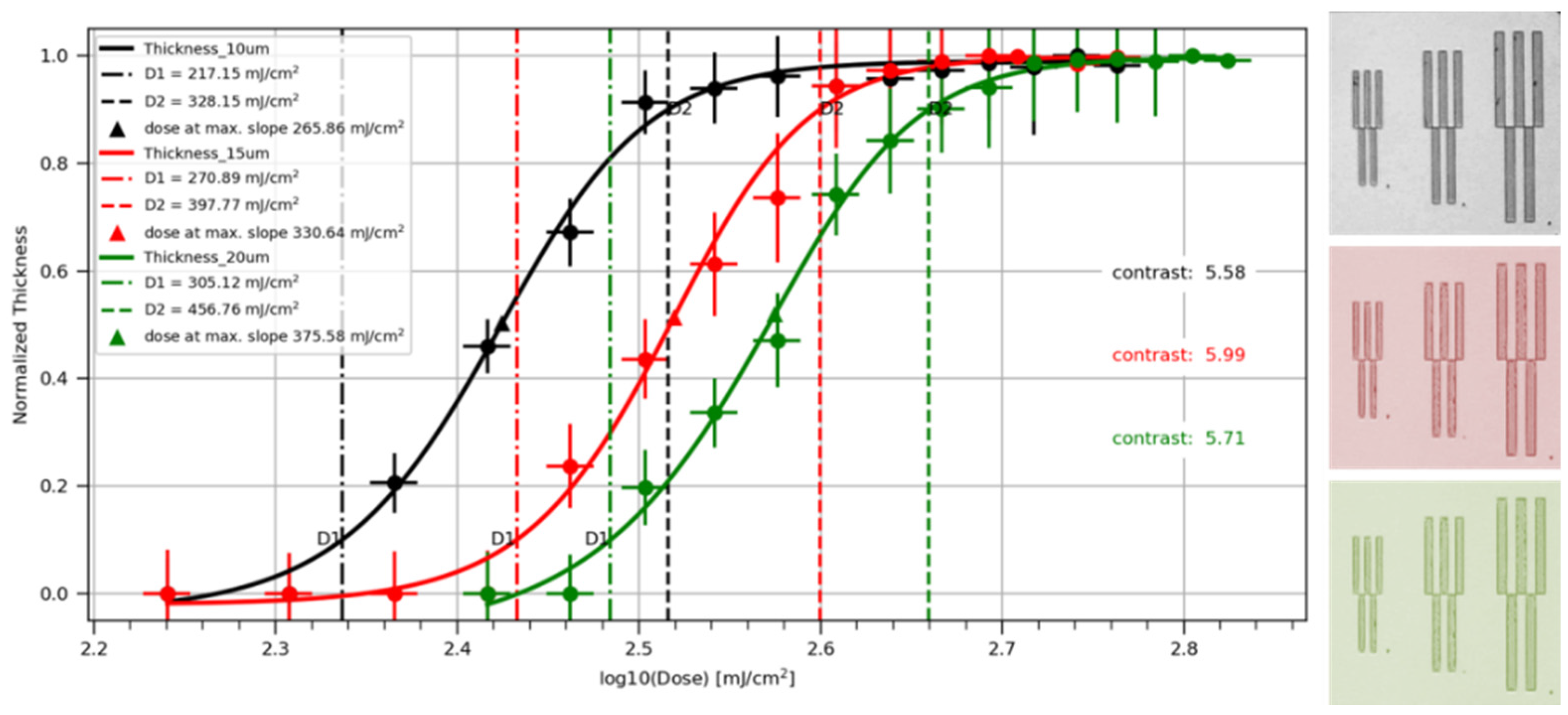
The results of the sensitivity curve measurements, which describe the remaining photoresist fraction as a logarithm function of the applied exposure dose, are shown in
Figure 1. To approximate the data, we used a generalized logistic function fit according to the approach reported previously [
18]. As one can see, the sensitivity curves for the 15 and 20 µm photoresist layers are shifted towards higher exposure doses. This is due to the absorption introduced by the photoresist layer, which decreases the delivered bottom dose. All curves exhibited a similar slope, which can be associated with photoresist contrast. The contrast value is defined by:
where
D1 is the dose for which the remaining photoresist height is 10% of the original value, and
D2 is the dose for which the remaining photoresist height is 90% of the original value. The value of the contrast generally represents the response of the photoresist to radiation [
18]. From the fabrication point of view, the most valuable information for a given patterning photoresist material is the optimal dose. By optimal dose, we mean the value that is sufficient to obtain a full cross-link of the photoresist. Optimal values were estimated from the sensitivity curve plateau, taking into account the pattern quality evaluated with an optical microscope (
Figure 1). Defect-free patterns were obtained at the optimal dose value, which also served as a confirmation of properly-adjusted PEB and development time conditions. As it was noted previously, the thicknesses higher than 20 µm could not be subjected to the sensitivity curve procedure; thus, the optimal values for such thicknesses were extrapolated from the data for lower thicknesses.
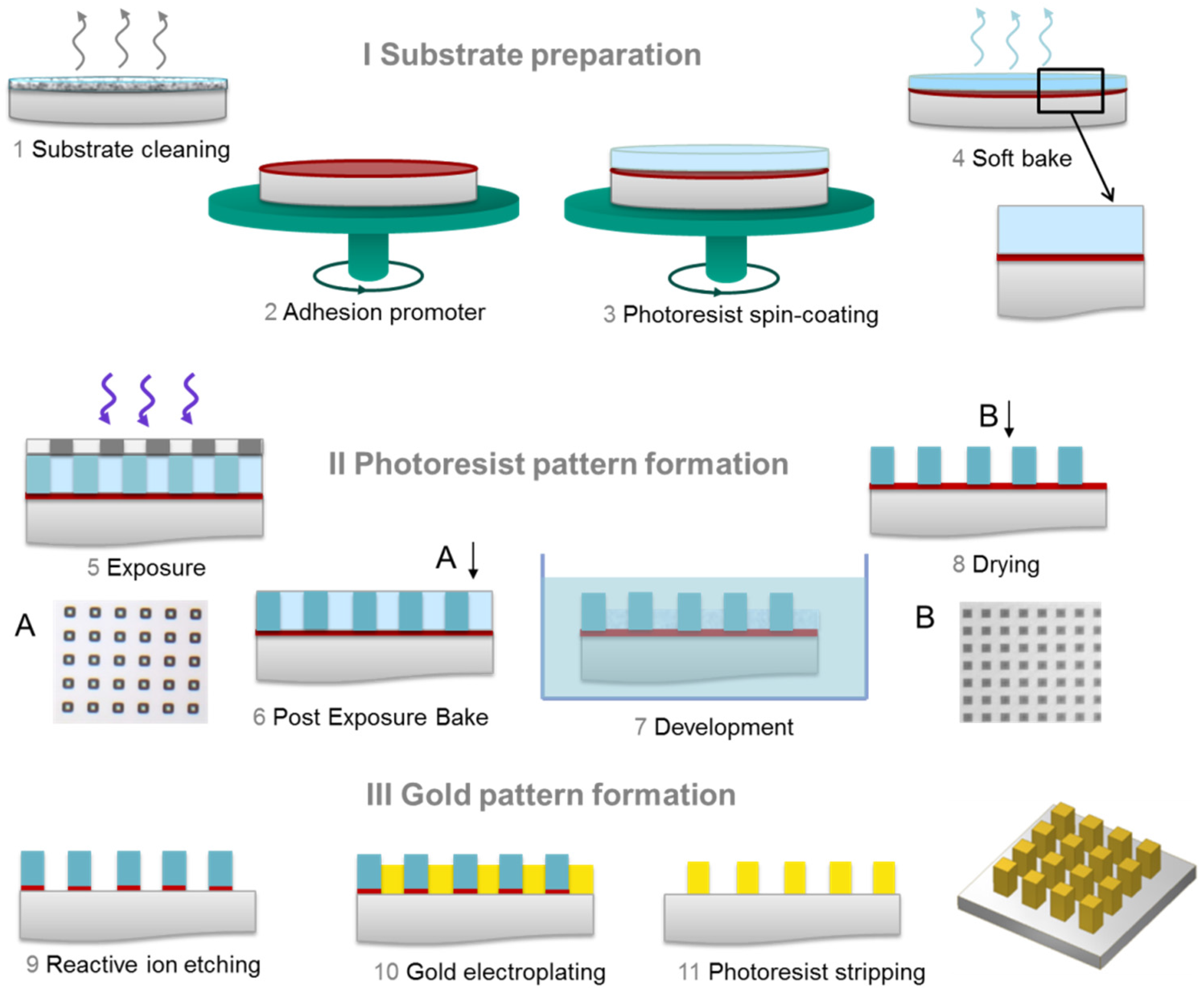
2.2. Grating Fabrication Process
UV lithography for manufacturing of two-dimensional (2D) gratings was carried out using the process chain similar to the contrast curve sample preparation, but with several application-related changes. The main overview of the process is shown in
Figure 2. Thinner silicon wafers were used for grating fabrication in order to achieve a higher wavefront modulation. The substrates were 200 µm silicon wafers with few nanometers of Ti and TiOx to create a conductive contact layer for the concluding electroplating. Substrate cleaning was performed to guarantee that it was free of impurities and moisture. Oxygen plasma cleaning was employed with subsequent baking at 120 °C and cooling to room temperature immediately before coating. Spin-coating of TI PRIME (MicroChemicals GmbH, Ulm, Germany) adhesion promoter was performed prior to photoresist application. TI PRIME forms a physically-bonded sub-monolayer of the active compound after solvent evaporation. A subsequent baking step of the primed substrate at 120 °C chemically activated the adhesion promoter, thus forming the desired hydrophobic surface allowing the subsequent photoresist coating with improved wetting and adhesion between the TiOx and the photoresist. Immediately after the primed substrate baking was finished, spin-coating of the negative mr-X 10 photoresist was performed to achieve layers of 10 µm, 20 µm, 30 µm, and 40 µm thicknesses. A soft bake to remove the solvent content from the sample was carried out at 95 °C on hot plates for time periods from 10 min to 20 min depending on the photoresist layer thickness.
2.2.1. Photoresist Pattern Formation
The exposure of photoresist layers was performed using EVG mask aligner (EV Group, Sankt Florian am Inn, Austria) with 2.85 mW/cm
2 radiation intensity (0.15 mW/cm
2 deviation) using the filter for wavelengths shorter than 365 nm. The photomask for exposure was a 5-inch Cr-Quartz mask purchased from Compugraphics (Jena, Germany) with four regions of different periods and shapes, and the area of each region was 1 cm
2. The exposure was carried out in soft contact mode (no vacuum) in order to prevent the sticking of the photoresist layer to the mask. The exposure dose values are listed in
Table 1. Theoretically, the optimal dose depends on the photoresist thickness, solvent, UV sensitivity, absorption in the exposure spectrum, power, and coherence of UV lamp, but for fabrication purposes it was empirically estimated using the sensitivity curve method. For thicknesses higher than 20 µm, the optimal dose values were extrapolated from the sensitivity curve data.
Post-exposure bake and development steps were the same as for the contrast curve sample set. Development times were adjusted according to the thickness of the photoresist layer. Optical microscope images of the gratings were obtained to perform a preliminary quality assessment of periodicity and homogeneity of the pattern. Sharp definition of the structures and a high degree of periodicity was observed for all periods for photoresist thickness up to 20 µm. However, for a photoresist thickness of 30 µm and thicker, structures with a period of 10 µm undergo undesirable crosslinking caused by the diffraction effect, which made square structures appear round. This resulted in structure size loss, as the final structures were electroplated using a structured photoresist layer as a mask for the conductive wafer surface.
2.2.2. Gold Electroplating
The photoresist mask formed by means of UV lithography was filled with gold in an electroforming step after development. Electroplating current density and voltage were fixed and the duration time defines the amount of gold that should be plated on the wafer. This amount of gold was determined by the height of the designed structures, which is usually 75–80% of the photoresist layer thickness, and the area that should be electroplated. Gold electroforming was performed using a standard gold-sulfite electroplating bath for microstructure fabrication at a temperature of 55 °C. After electroplating, the photoresist was stripped using oxygen plasma.
The manufactured gratings and their main characteristics are listed in
Table 1. Each grating has an area of 1 cm × 1 cm, as defined by the mask layout. However, larger areas (up to 5 cm × 5 cm) can be obtained within the same process chain if the respective mask layout is used.
4. Discussion
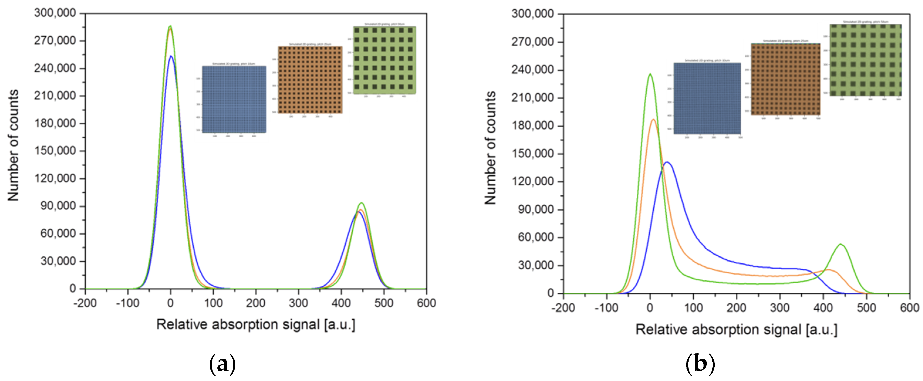
To understand the data obtained from the measurements and evaluate the quality of the microstructure patterns over a large area, we correlated the grating defects and flaws with respective projection image distortions. In order to investigate possible generalized imperfections of the grating and its alignment in the setup, ideal data arrays were simulated, and their changes caused by the introduction of rotation and blurring were analyzed in terms of the absorption signal histograms. It is important to note that the proposed quality evaluation algorithm is giving useful information only for intrinsically periodic structures, such as gratings.
The main idea of the grating quality evaluation algorithm was to test the grating in a radiography setup to compare the intensity distribution obtained on the detector plane with the simulated intensity map from an ideal grating. By modifying the simulated ideal grating, one can estimate, quantitatively, the intensity modulation and characterize structural changes in the real grating. Using a simplified empirical model, an ideal grating was represented by a two-dimensional array of data with exactly the same dimension as the digital image obtained from the real data files acquired with the detector, taking into account the magnification. The array was filled with a constant value, and an intensity distribution histogram was obtained. This gave a discrete spectrum consisting of two peaks at absorption signals for the wafer (if normalized by the absorption level of the wafer, this peak is centered at zero) and the gold structures. The ratio of peaks is 1:3, as the gold structures cover one-third of the illuminated grating area in the simulated experiment.
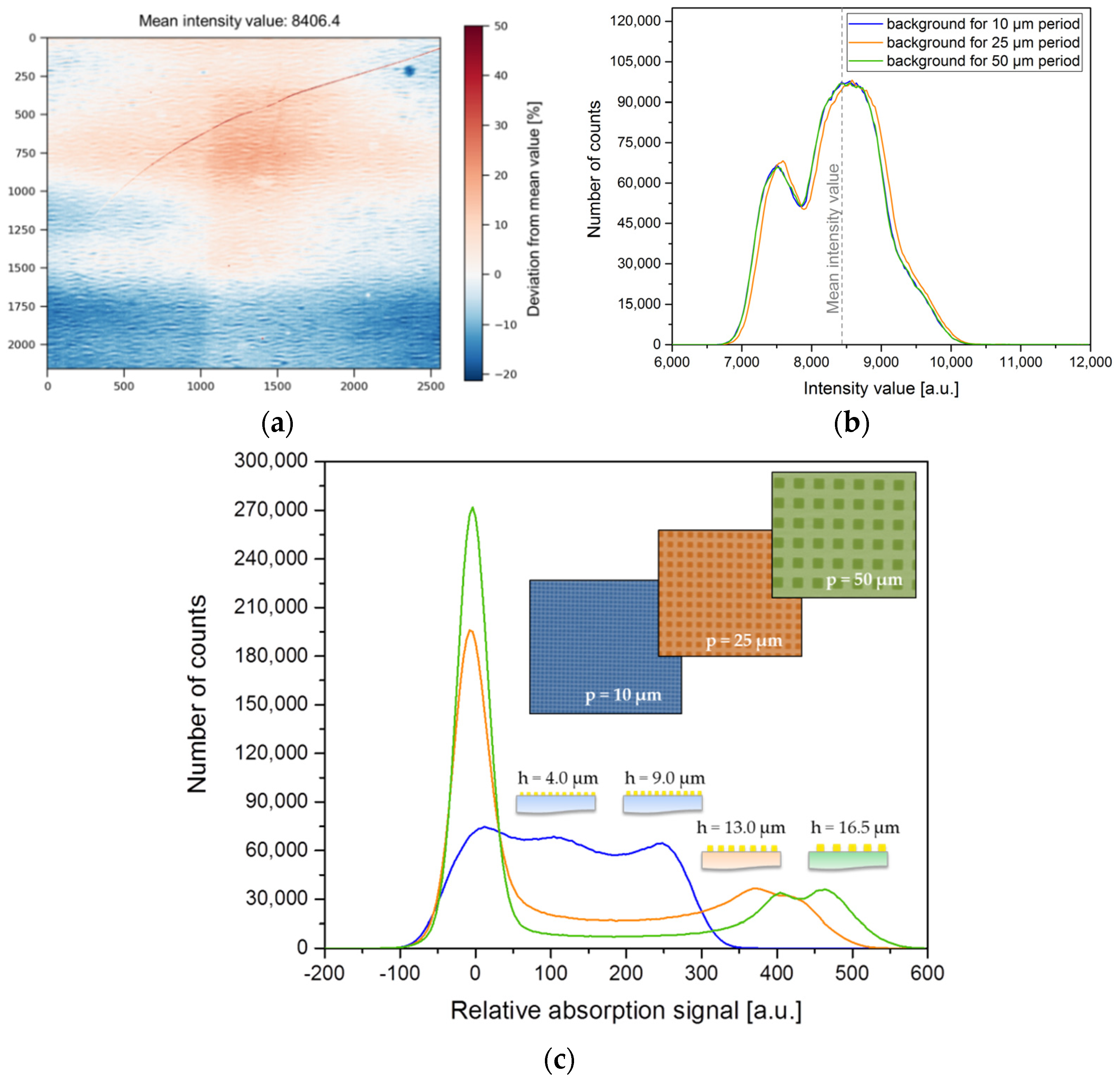
When the arrays and associated intensity distribution histograms were obtained, the approximation of real gratings was achieved by adding a background function representing noise introduced by the experimental setup. This was done by introducing random fluctuations around the central value as detector noise (Gaussian distribution) or by using a real signal recorded by the detector in the experiment. The intensity distribution histogram with added noise is shown in
Figure 7a. As the grating was supported by the substrate, it introduced a certain absorption, which decreased the signal-to-noise ratio and could also be treated as a contribution to the background. The detector noise was further estimated together with the contribution of 200-µm-thick silicon absorption, thus, the histogram peaks were shifted in a way that the zero position corresponds to the radiation passing between the grating structures, and the second peak was placed at the absorption level of the gold structures, which was determined by the gold height.
However, in reality, not only does the presence of the detector noise decrease the efficiency of the intensity modulation, but also causes blurring by the imperfectly steep profile of structure sidewalls. Note that this manufacturing-driven blurring is independent of the blurring of the projected grating edges by the source focal spot size (focal spot size in case of an X-ray tube or lens focusing spot for a lens system). Despite the different origin, both result in blurring of the projected image, which is stronger for smaller periods: one can see that for the simulated grating with a 10 µm period that the intensity distribution is not discrete anymore and peaks associated with the absorption of the wafer and the structures are merged and are not clearly distinguished, as can be seen in
Figure 7b. The histogram shown in
Figure 7b has been obtained by varying the input parameters, such as the in-plane rotation of the grating and blurring of the image to match the experimental conditions and decouple the influence of generalized pattern defects from local imperfections. As one can see from the projection images shown in
Figure 6c, there was a slight in-plane rotation of the grating present when the grating was placed in the holder. The rotation angle of 0.6 degrees was included in the empirical simplified model to better represent the acquired images and account for smoothening of the ripples in the histogram.
It is important to emphasize that the simulated data only included general distortions uniformly applied to the entire pattern and no local defect impact was considered. By comparison of the histogram obtained from the experimental data (
Figure 6c) and the simulated one (
Figure 7b), it is clearly seen that the pure pattern blurring cannot explain the distribution obtained for the gratings. In particular, the splitting of the peaks corresponding to gold absorption, especially evident for the 10 µm period grating (
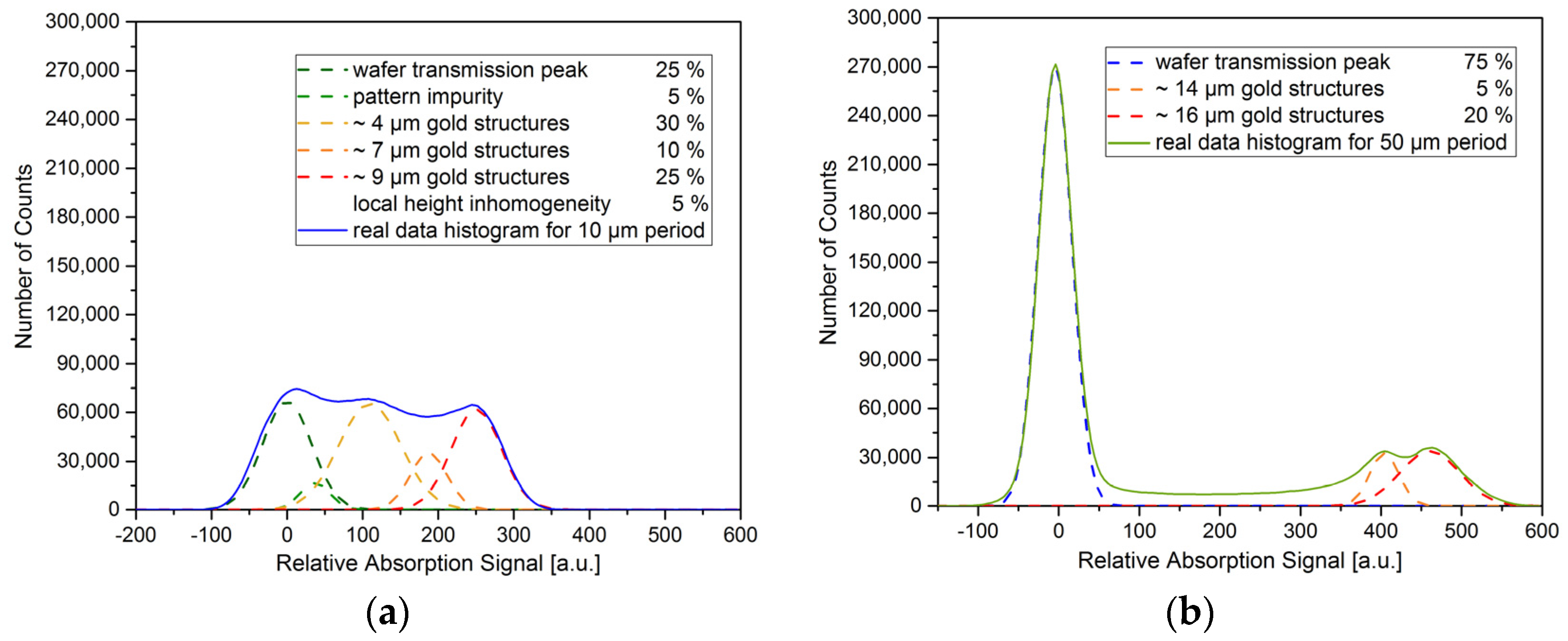
Figure 8a), cannot be attributed to uniform effects present in the pattern but, rather, local defects of mainly random and rare appearance. One kind of such an effect is gold overplating, which causes the appearance of higher absorption levels. However, at the designed X-ray energy, the gold structures, with an average height of 15 µm, transmit only 0.5% of the incoming radiation [
20]. This means that the gold structures higher than 14 µm will not make a considerable effect on the intensity modulation. Overplated structures that contribute to the gold pillars higher than 20 µm will not make any impact on the absorption signal histograms obtained from the measurements at the energy of 8.5 keV.
Another local effect present at the characterized gratings is pattern impurity due to partial gold deposition between the structures, which led to an overall decrease in transmission, thus, a decrease in intensity and additional broadening of the zero-centered peak. To analyze this effect in greater detail, the decomposition of real data histogram profiles into several Gaussian-shape signals has been performed. Examples for 10 µm and 50 µm period gratings are shown in
Figure 8. It is evident in
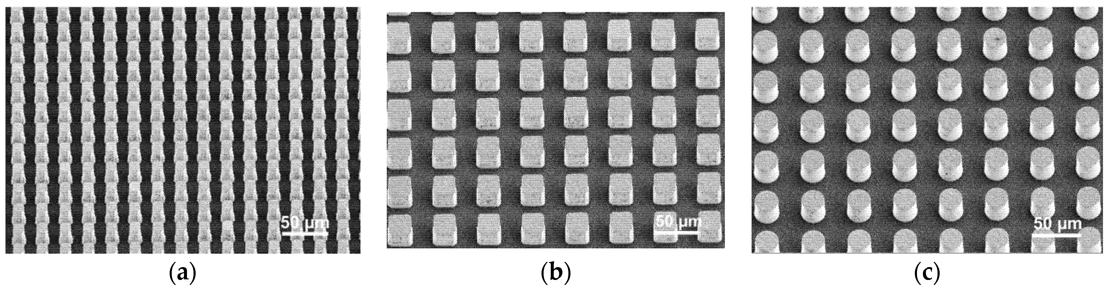
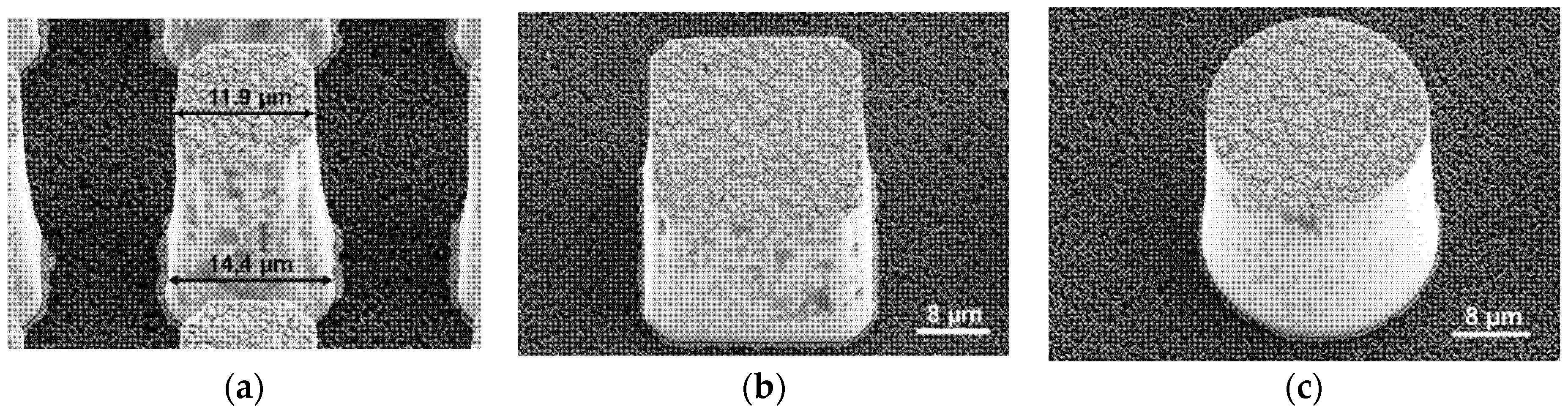
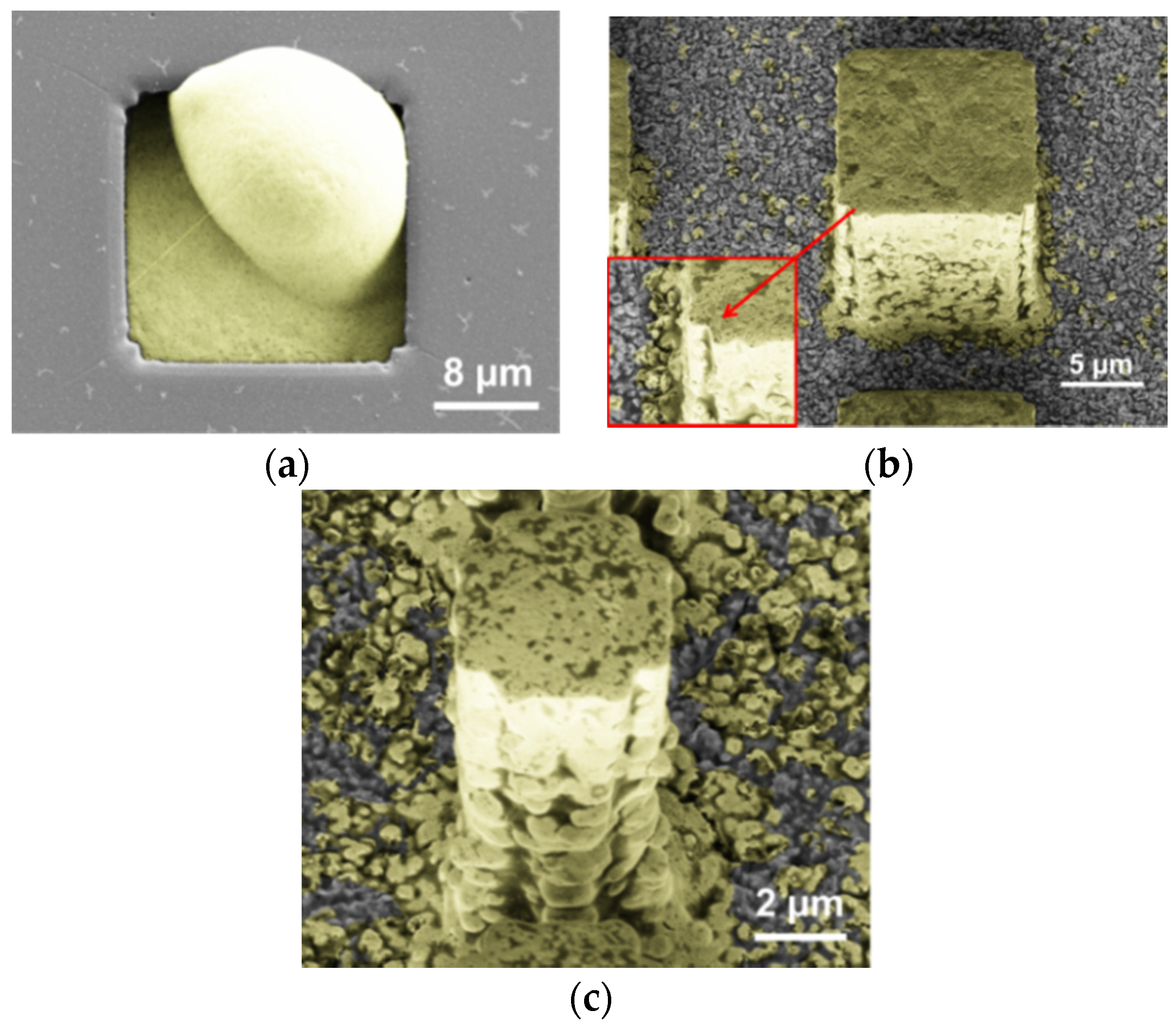
Figure 8a that an additional contribution of the signal at approximately 30 a.u. is present, corresponding to the gold height about 1 µm. This signal is attributed to the impurity of the pattern and contributed to the broadening of the zero-centered peak. The impurity of the pattern for the tested grating might be due to a slight undercut of the photoresist layer during reactive ion etching prior to electroplating. The effect was stronger for smaller periods, as observed with SEM (
Figure 5b,c), in this case the gold nucleation points were placed closer to each other, and undesirable diffusion of Au
+ between the structures in the undercut area occurred. In turn, the contrast between absorbing and non-absorbing areas on the projected images was strongly decreased by this effect for smaller periods. For example, for the 10 µm period grating, the highest pillars were about 9 µm (
Figure 5c), thus, approximately 5% of the radiation was transmitted through such structures, and the transmission of the wafer carrier was reduced by the impurities of the pattern, resulting in a decreased intensity modulation.
However, not only did impurities contribute to the overlapping of the peaks on the histogram for 10 µm period; as it was mentioned above, there is a third Gaussian centered at approximately 110 a.u. (the yellow dashed line in
Figure 8a), which can be correlated with the gold height of about 4 µm using information obtained with SEM. This implies that the gold height is not homogeneous and pillars of different height were obtained during the electroplating. However, for the 50 µm period grating, the intensity modulation was highly efficient, resulting in clearly separated signals from gold structures and the transparent areas with the ratio of 1:3. Nonetheless, a splitting of the signal in two Gaussians is present, attributing to 14 µm and 16 µm heights. Another defect that could cause changes in the distribution of the absorption signal is the diffraction-caused shape distortion, which is prevailing for the 10 µm period grating. This effect can be diminished by using a circular-shaped mask for UV lithography, as such a shape is less sensitive to diffraction effects.
5. Conclusions
In this work, the technological process for fabrication of two-dimensional X-ray gratings is described. The fabrication process is based on UV lithography and gold electroplating. Absorption gratings represented by periodic free-standing gold pillars with lateral structure sizes from 5 µm to 25 µm and heights from 5 µm to 28 µm have been manufactured. The gratings have shown a high degree of periodicity and defect-free patterns which enables their application for single-shot X-ray phase-contrast imaging. The gold height achieved in the manufacturing process absorbs more than 90% of X-ray radiation at the energy of 25 keV; for the transmission of 200-µm-thick silicon substrate at this energy the WFM is about 0.8, which implies that the manufactured gratings can be used for single-shot imaging at energies up to 25 keV.
An algorithm allowing the qualitative and quantitative characterization of homogeneity and uniformity of the micropattern over a large active area involved in the imaging measurement was developed. The simulated images include general effects like blurring, detector resolution limitations, noise, and misalignments. However, they do not include any information on local defects, such as the diffraction-induced shape distortion, overplating, pattern impurity, mask defects transferred to the final grating, etc. Such defects are becoming critical for small periods, like 10 µm, as can be seen by comparing the real data histograms with the simulated data, while larger periods are less affected by the abovementioned defects and exhibit clear intensity modulation. From the evaluation of the grating structures in the radiographic setup, it follows that two-dimensional gratings with periods of 50 µm and 25 µm exhibit clear patterns and can be used for single-shot X-ray phase-contrast imaging at energies up to 25 keV. The gratings with 10 µm period have multiple manufacturing-driven defects and require further quality improvement, for example, by using deep X-ray lithography or improved photoresist formulations. The evaluation of the grating quality will also be further improved, most probably introducing an image pattern recognition algorithm to be sensitive to small, localized defects.
The findings reported in this paper can be used for the improvement of image quality and broadening of applications for X-ray phase-contrast single-shot imaging towards materials characterization and medical imaging. The developed algorithm could also provide additional information on the grating quality by utilizing single projection for easier data interpretation during measurements of various objects.

 ,
, 


