1. Introduction
Extreme ultraviolet lithography is being industrialized as the next candidate printing technique for high-volume manufacturing of scaled down microcircuit devices for logic and memory applications. Because of the short wavelength of 13.5 nm used in extreme ultraviolet (EUV) lithography, it is not possible to use refractive optics or transmission masks for image formation, and the optical elements and EUV photomask are reflective mirrors. The EUV mask is a reflective multilayer (ML) mirror, consisting of molybdenum/silicon (Mo/Si) bilayers having peak reflectivity at 13.5 nm, and is coated with a mask absorber where light has to be attenuated. The chief-ray incidence angle on mask is set at 6° from normal to avoid overlap of incident and reflected light.
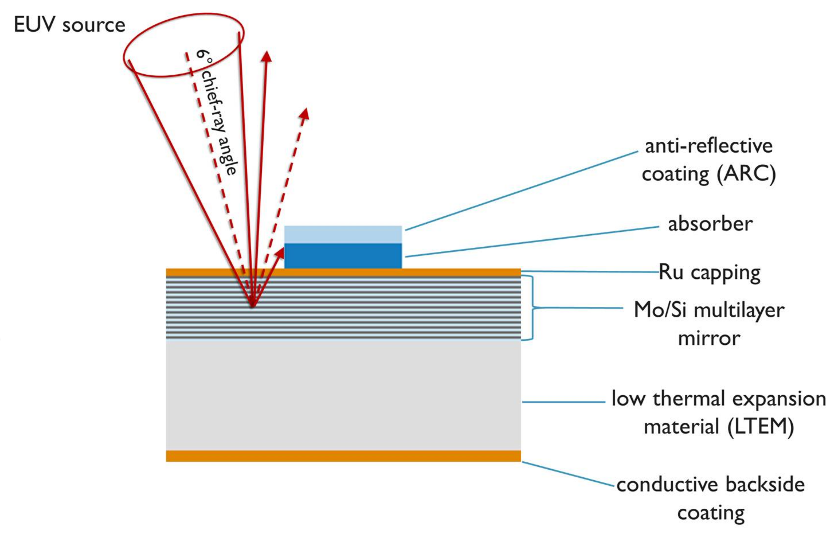
Figure 1 depicts the cross-section of an EUV photomask. The substrate consists of a low thermal expansion material (LTEM) glass plate with a Mo/Si ML mirror coating on front side, and a conductive backside coating for electrostatic chucking. A thin ruthenium (Ru) capping layer protects the mirror against oxidation of the top Si layer, and against the cleaning of organic contaminants by hydrogen reduction [
1]. Currently, tantalum (Ta) is the main component of most common absorber materials developed for commercial EUV photomasks. The absorber layer is etched into a pattern to be printed on wafer, and is capped with an oxide anti-reflective coating (ARC) to create contrast between the absorber and the mirror for defect inspection in the deep ultraviolet wavelength range (DUV).
The combination of EUV light at oblique incidence, absorber thickness, and non-uniform mirror reflectance through incidence angle, creates photomask-induced imaging aberrations, known as mask 3D (M3D) effects [
2]. These effects are experimentally observable, as feature orientation-dependent shadowing effects [
3], best focus variation through pitch [
4], feature size-dependent pattern shift through focus [
5,
6], and pattern asymmetry and contrast loss [
7]. Selecting the correct mask absorber material and thickness helps in reducing M3D effects [
2,
8,
9]. This approach is complementary to other M3D mitigation strategies, such as source optimization [
10], sub-resolution assist feature placement [
11], and transition to anamorphic high-NA EUV lithography [
12].
This paper will focus on absorber material as a mitigation strategy for M3D effects, and we verify whether mask absorber materials with high extinction coefficient κ and refractive coefficient n close to unity can be generated by combining Al and Ni in an alloy. The motivation for this particular material selection is explained in the next section.
In
Section 2, we review the material selection criteria, and methods to deposit and characterize the alloys. In
Section 3 we elaborate on the film characterization results, such as film morphology and material durability. Composition and density profile are determined to calculate the optical constants, which will be experimentally verified with EUV reflectometry (EUVR). The comparison between the calculated and measured optical constants will be discussed in
Section 4. In
Section 5, the measured optical constants are incorporated in an accurate mask model for rigorous imaging simulations to determine M3D imaging impact. Finally, we summarize our findings and give an outlook in
Section 6.
2. Materials and Methods
Novel EUV absorber materials are primarily chosen for their optical performance in the EUV wavelength range, which is described by the complex refractive index. The imaginary part
κ or extinction coefficient determines the attenuation, while the real part
n or refraction coefficient determines the phase velocity. To reduce mask absorber height-dependent M3D effects, a material that absorbs more EUV and has higher
κ than Ta is necessary [
2]. Best focus shifts through pitch are caused by phase distortion due to a mismatch in refraction coefficient
n at the vacuum and absorber interface, hence a material with
n close to unity is preferred [
13]. In this paper, the focus will be on material selection for BIM, i.e., high
κ and
n close to unity.
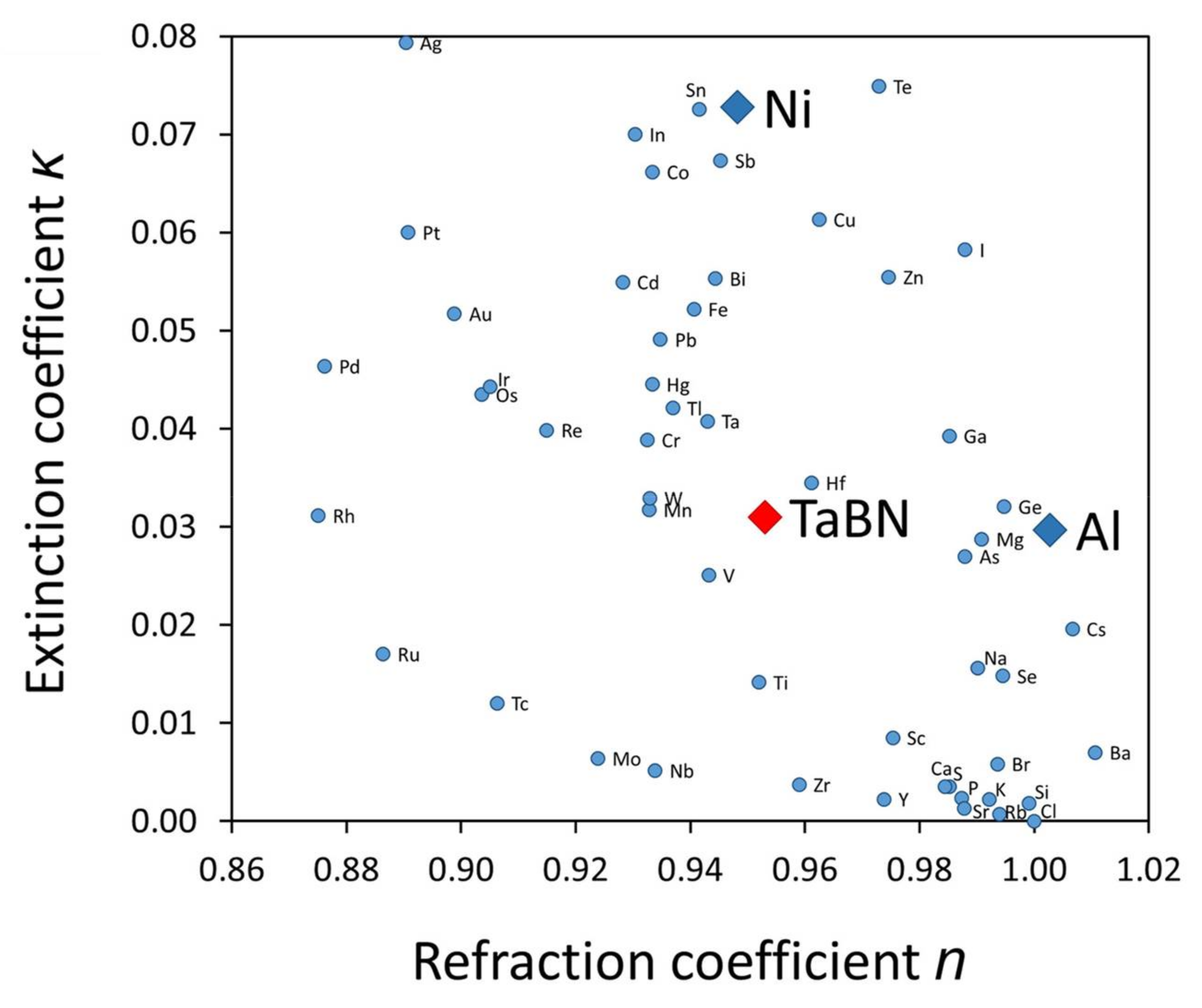
Figure 2 shows the relationship between
n and
κ at 13.5 nm EUV wavelength of elements from Z = 11 to Z = 83, excluding elements from the lanthanide series and noble gases [
14]. Nickel (Ni) is one of the highest EUV absorbing elements, but it can easily form crystal grains [
8,
9,
15]. Alloying is an option to reduce Ni crystallinity [
16]. Aluminum (Al) has non-negligible EUV absorption and
n larger than unity. Based on rigorous imaging simulations, Al is expected to reduce M3D effects [
17,
18], but imaging contrast will deteriorate due to Al’s lower
κ compared to Ta. By combining both elements into a Ni
xAl
y alloy, we target a material that reduces EUV phase distortion, while maintaining good contrast for imaging at reduced absorber thickness.
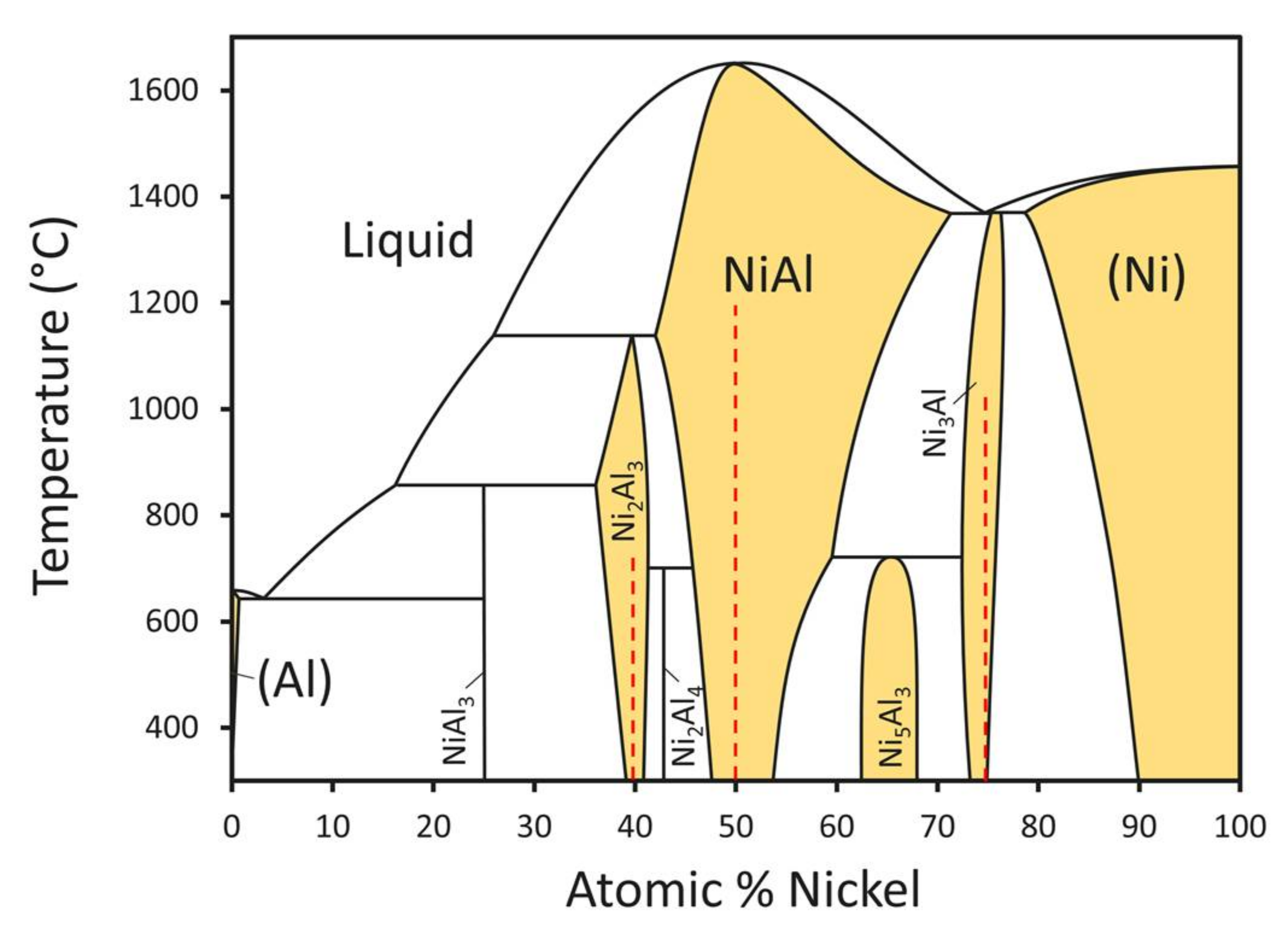
Based on the thermodynamic phase diagram of Ni-Al system in
Figure 3 [
19], three stable Ni-Al compositions were investigated: Ni
3Al, NiAl and Ni
2Al
3. The films were deposited with a nominal film thickness of 25 nm by physical vapor deposition (PVD) through co-depositing Ni and Al targets. We used 6” Si-wafer substrates on which 30 nm SiO
2 was grown through wet oxidation. The wafers were mounted on a rotating wafer drum, sequentially passing Ni and Al direct current (DC) plasma’s at Ar pressures of 5.10
−3 mbar resulting in alternating Ni and Al monolayers deposited and instantaneous intermixing. Furthermore, when selecting new EUV absorber materials, they need to satisfy a set of specifications summarized in
Table 1 [
8,
17]. We present detailed results of the characterization with respect to some of these properties. Determining the optical constants of the absorber material with EUV reflectance requires an accurate absorber stack model, for which additional metrology is needed to assess the chemical composition and density profile of the absorber film.
The absorber film morphology is preferably nano-crystalline or amorphous, which is challenging to achieve for most single metals. Crystallinity however, is very likely to impair surface roughness and etch bias. Preferential etching along crystal grains can cause increased absorber line edge roughness (LER) and lead to critical dimension (CD) variations, which will be transferred to wafer [
27,
28]. Additionally, absorber morphology affects mechanical film stress. Stress induced by absorber, and ML mirror must be controlled within a range of ±180 GPa to ensure the flatness of the photomask [
19] and to avoid distortion-induced pattern placement error [
29]. Doping or alloying with additional elements, or a multilayered absorber structure are possible solutions to reduce crystallinity [
15,
30]. We have measured alloy crystallinity using X-ray diffractometry (XRD) and transmission electron microscopy (TEM).
During processing, temperature must be below 150 °C to avoid intermixing between the mirror’s Mo/Si bilayers to maintain high EUV reflectance [
22]. This constraint limits deposition of the absorber film to PVD, as most chemical deposition techniques require high temperature [
31]. The low temperature during PVD, causes the material deposition to be mainly kinetically controlled. Most atoms will lack the energy to arrange themselves into the most efficient close-packed lattice. Hence the crystal density as reported for the thermodynamically stable crystalline compound will likely not be obtained.
Anisotropic etch of the absorber material must be capable of forming well defined patterns with straight sidewalls. Reactive ion etch (RIE) ensures these conditions, but requires the absorber material to chemically react with the etchant gas and to form volatile compounds below 150 °C. Materials with small CD difference before and after etch are preferred [
32,
33]. Furthermore, the absorber material must have good adhesion to the Ru capping layer, even during cleaning, and with good etch selectivity to Ru.
Etch development of alternative metals is an important challenge to solve. Despite good imaging performance and durability, Ni remains difficult to pattern. Physical sputtering has limited etch selectivity and cannot obtain the required pattern quality, due to uncontrolled redeposition of non-volatile Ni particles, resulting in sloped sidewalls and Ni residues on the mirror [
9]. However, Ni can form volatile organo-metallic compounds at low temperature [
34,
35], and emerging etch technology, such as atomic layer etch (ALE), can be promising for enabling transitional metal plasma etch [
36]. Alternatively, a damascene-like additive patterning scheme can be adopted to circumvent the direct Ni etching [
37]. This solution requires the ability to remove the template pattern selectively afterwards. Furthermore, the ability to form volatile Ni compounds induced by electron beam is still necessary for absorber defect repair of such Ni patterns.
The absorber must remain inert in the EUV scanner ambient, and at the elevated temperatures during EUV exposure. It is not allowed to transform into a different solid phase to avoid volumetric changes. A phase transition of Ni
xAl
y alloy is unlikely below 150 °C though (cf.
Figure 3), as both elemental Ni and Al have melting points much higher than the thermal budget for EUV photomasks. H
2 is used inside the projection optics (PO) box in EUV scanners [
38]. Although the photomask is physically outside of the PO box, concerns remain on their capability to react with hydrogen under EUV exposure. A first estimation for the hydrogen durability of an element, is by assessing the volatility or melting point of its hydrogen compound. This assessment however, does not give information on kinetics or ease of formation of such compounds under scanner conditions. Hydrogen resistance can be additionally improved by doping with reduction resistant elements [
39]. We have tested hydrogen compatibility by exposing the alloy samples to H* radicals for 110 h. Composition changes after the durability tests were measured with RBS for Ni detection and elastic recoil detection analysis (ERDA) for Al detection.
For mask defect inspection in the DUV wavelength range, an oxide ARC is required to create contrast with the mirror where the absorber material has been etched away. For actinic inspection, the ARC layer is not necessary [
40]. Another function of the ARC layer is to limit the native oxide growth of the absorber material. For defect repair the absorber material must be able to form volatile compounds by electron beam-induced chemical reaction [
41]. Alternatively, nanomachining repair can remove non-volatile materials, but is less selective [
42]. The absorber must remain stable under cleaning conditions, preferably basic solution to prevent the Ru capping layer from oxidizing and peeling [
25]. The introduction of pellicles in EUV lithography will likely reduce the number of cleaning cycles necessary during the lifetime of an EUV mask. In this paper, we have tested cleaning compatibility of Ni
xAl
y alloy samples by 24 h submersion tests in DIW, and in NH
4OH.
Finally, the optical constants are determined through calculation with Equation (1), and through experimental verification with EUVR. Equation (1) relates the optical constants to the semi-empirically determined atomic scattering factors through wavelength as follows:
with
r0 the classical electron radius,
λ the wavelength,
NA Avogadro constant,
ρalloy the alloy density,
wj and
Mj the weight percentage and molar mass of the
jth element respectively,
f1,j and
f2,j the real and imaginary part of the forward atomic scattering factor of the
jth element respectively, tabulated by Henke et al. [
14]. To use Equation (1), one needs to know first the elemental composition, through
wj, and density
ρalloy, which are characterized by X-ray photoelectron spectroscopy (XPS), X-ray reflectometry (XRR) and TEM with energy dispersive X-ray analysis (TEM-EDS), as tabulated in
Table 2.
In the second method, the optical constants are fitted from EUVR measurement through wavelength and through incidence angle. An accurate stack model as a starting point, with correct number of layers and layer thicknesses, can improve fitting convergence towards a set of optical constants. Such a stack model has been verified with XRR and TEM.
3. Film Characterization
In this section, we present and elaborate on the film characterization results. We investigated film morphology, material durability, composition and density profile, using metrology as defined in
Table 1 and
Table 2. Composition and density profile results will be used to setup models for extracting optical constants in
Section 4.
3.1. Film Morphology
The degree of crystallinity of the as-deposited film provides an estimation for the susceptibility to surface roughness and LER. The absorber morphology is preferably nano-crystalline or amorphous, and can be determined using cross sectional TEM and XRD.
Figure 4a displays the cross-section TEM images of Ni
3Al, NiAl and Ni
2Al
3. An amorphous native oxide layer is clearly visible on the sample surface, which grows thicker with increasing Al-ratio. All Ni
xAl
y compositions are polycrystalline, which can be observed as contrast and lattice orientation change in the Moiré patterns.
Figure 4b presents the same samples under different magnification and contrast to better visualize the crystal grains. Ni
3Al and NiAl have similar crystallinity with columnar grains spanning the full film thickness. Ni
2Al
3 exhibits smaller grains near the surface and substrate interface.
Crystallinity is further investigated with XRD scans in Bragg–Brentano geometry, which is mostly sensitive to lattice planes parallel to the film surface. The atomic planes of a crystal cause incidence X-rays to diffract in specific angles. The most intense diffraction peak of a reference Ni film of 25 nm is located at 44° 2theta, which is caused by Ni (111) oriented lattice planes. The full width at half-maximum (FWHM) of the Ni (111) peak can be used to estimate the average crystal grain size
τ through the Scherrer’s equation [
43], with
K the crystal shape-dependent Scherrer constant,
λ the Cu Kα X-ray wavelength, and
θ the X-ray incident angle corresponding to the observed XRD peak:
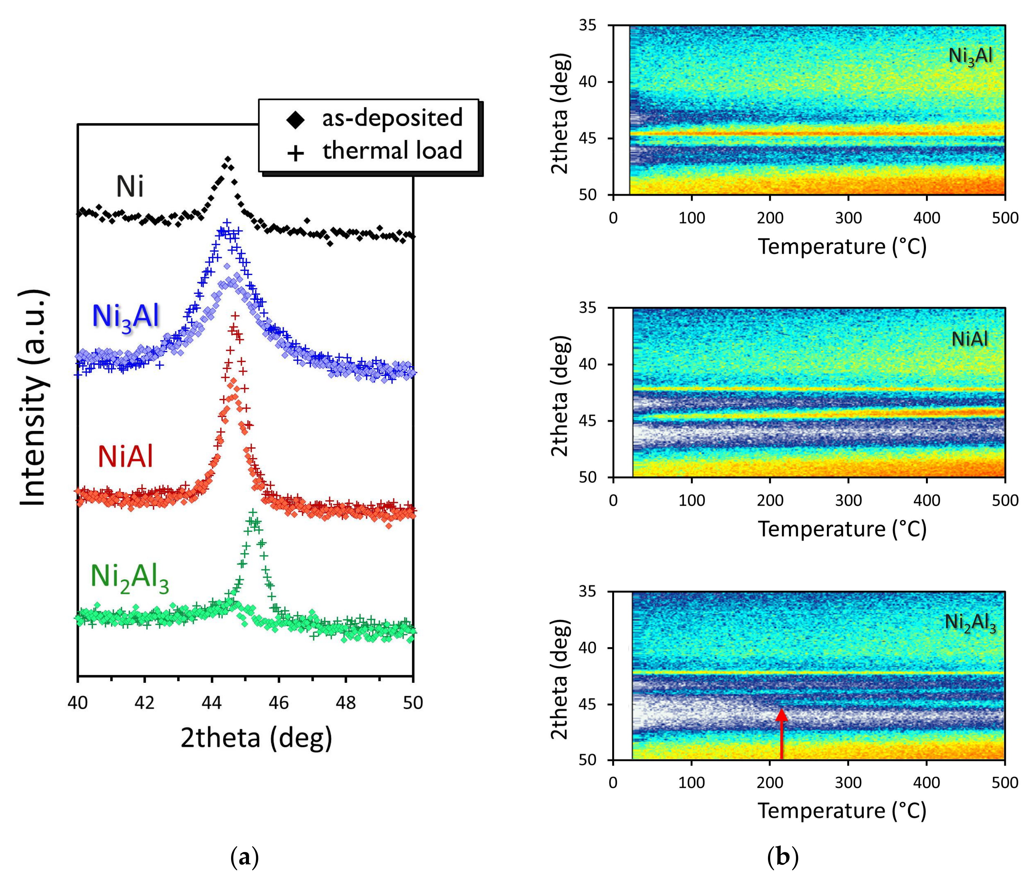
The XRD spectra of NixAly films are compared with a reference 25 nm thick Ni film, and are monitored with in-situ XRD (IS-XRD) during thermal loading up to 500 °C. After cooling down to room temperature, the XRD spectra of the NixAly films are measured again.
Figure 5a compares the XRD spectra of the as-deposited films, and of the films after thermal loading. Peak fitting results and estimated average grain size are tabulated in
Table 3.
Compared to the reference Ni (111) peak, the peak of as-deposited Ni3Al appears much broader, indicating smaller Ni3Al crystal grains. As-deposited NiAl exhibit a peak more similar to the reference Ni film. For as-deposited Ni2Al3, no clear XRD peaks can be observed, indicating poor condition for diffraction. Possible causes include nano-crystallinity, more variation in average grain size, and random orientation of the crystal lattice. After thermal loading and cooling down to room temperature, the peak position of both Ni3Al and NiAl remains the same, indicating no crystalline phase change occurred. The peak width has decreased slightly, suggesting the crystal grains have grown. The Ni2Al3 peak however, has shifted and increased significantly in intensity after thermal loading, indicating recrystallization into a different crystalline phase.
Figure 5b confirms Ni
2Al
3 recrystallization started after 200 °C. Taking the IS-XRD results into consideration, it is unlikely that a mask absorber comprising of only Ni and Al, will remain amorphous under working conditions. However, we have achieved a reduction in crystal grain size by alloying Ni with Al under unequal nominal Ni:Al ratio.
3.2. Durability
The photomask material must remain stable under cleaning conditions and working scanner conditions during the mask lifetime.
The initial cleaning durability test composes of submerging samples in two solutions with different acidity: DIW (slightly acidic pH 5.7 due to CO
2 diffusion from atmosphere) and NH
4OH (basic pH 11.4). Hydrogen durability was tested by exposing samples to a flow of H* radicals over a period of 110 h. H* radicals were formed through cracking H
2 with a hot tungsten filament using a EUV Tech hydrogen cleaner [
24]. After the durability tests the samples, together with a reference, were measured with XRR and RBS/ERDA to assess thickness and composition changes respectively. The results are depicted in
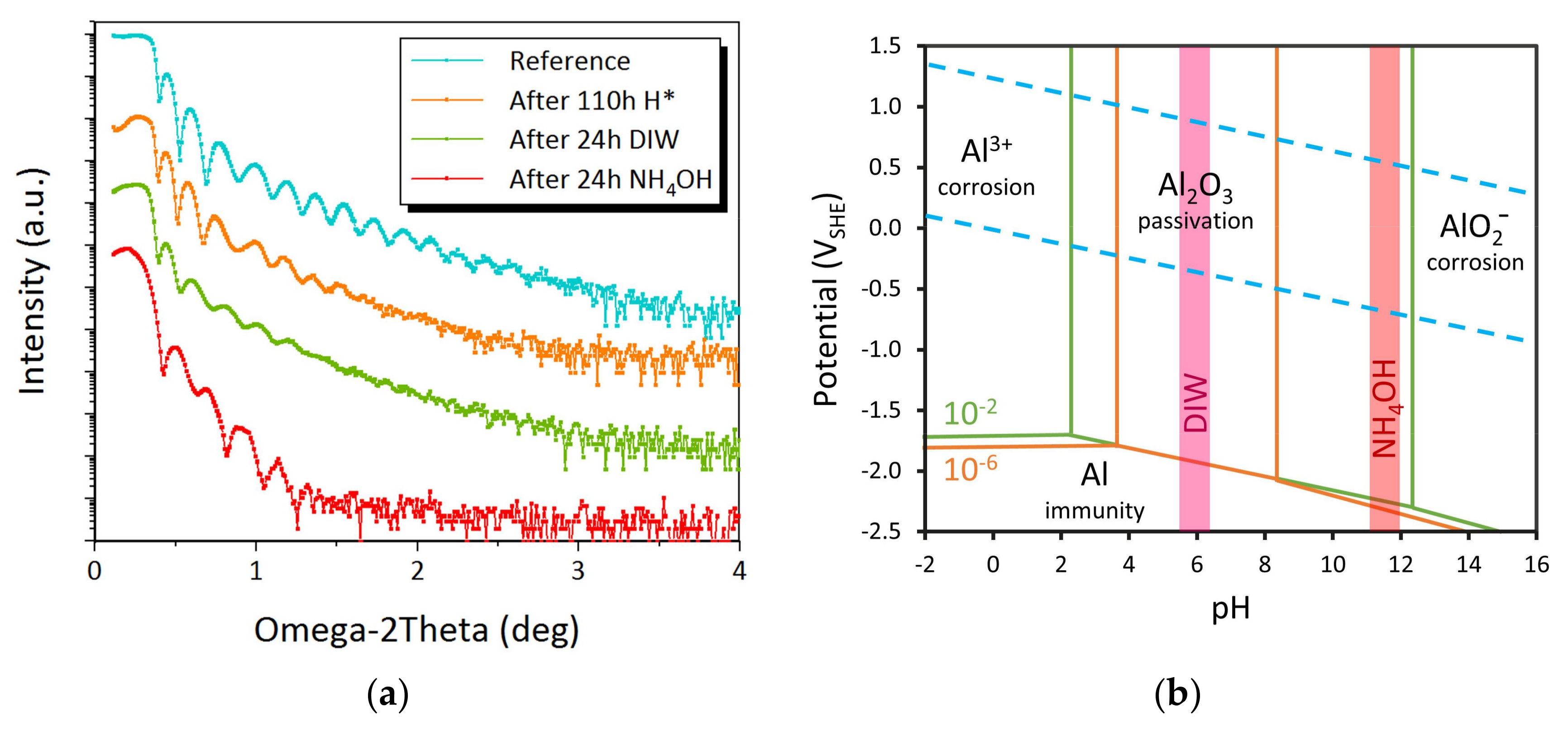
Figure 6a.
The XRR spectra of Ni
3Al reference and after 110 h H* have the same oscillation frequency, indicating no thickness loss. There is a slight increase in roughness after H* test, which can be recognized as attenuation of the amplitude at higher incident angles. Attenuation is also observed in the samples after 24 h in DIW, and even more so in NH
4OH. Furthermore, a reduction in oscillation frequency indicates a film thickness loss for the sample in NH
4OH. The Pourbaix diagram shown in
Figure 6b, helps understanding the behavior of Al in aqueous solution [
44]. The thermodynamic stable phases of Al are shown in relation to the solution’s electrochemical potential V
SHE, acidity pH, and effective concentration of the soluble species (Al
3+ and AlO
2−). The stability region of water lies between the dashed blue lines, which define the reduction and oxidation reaction of water. Under negative V
SHE or highly reducing condition, metallic Al is immune to reaction in aqueous solution. Under more oxidizing condition, Al will react depending on the acidity. Highly acidic and highly basic condition will dissolve Al into soluble Al
3+ and AlO
2− ions respectively, causing corrosion of the surface Al. Therefore, a thickness loss and increased roughness are observed by XRR for the sample in NH
4OH. Around neutral pH, Al reacts by forming an Al
2O
3 layer that functions as a stable passivation layer against corrosion. Based on XRR measurement, the passivating Al
2O
3 layer causes increased roughness. The pH-range of the passivating region is also dependent on the concentration of Al
3+ and AlO
2− in the solution. The driving force for Al dissolution is larger in diluted solutions, resulting in a small passivation region between pH 4 and 8 (orange line). Solutions with high Al
3+/ AlO
2− concentration, can increase the passivation region even more towards basic conditions (green line).
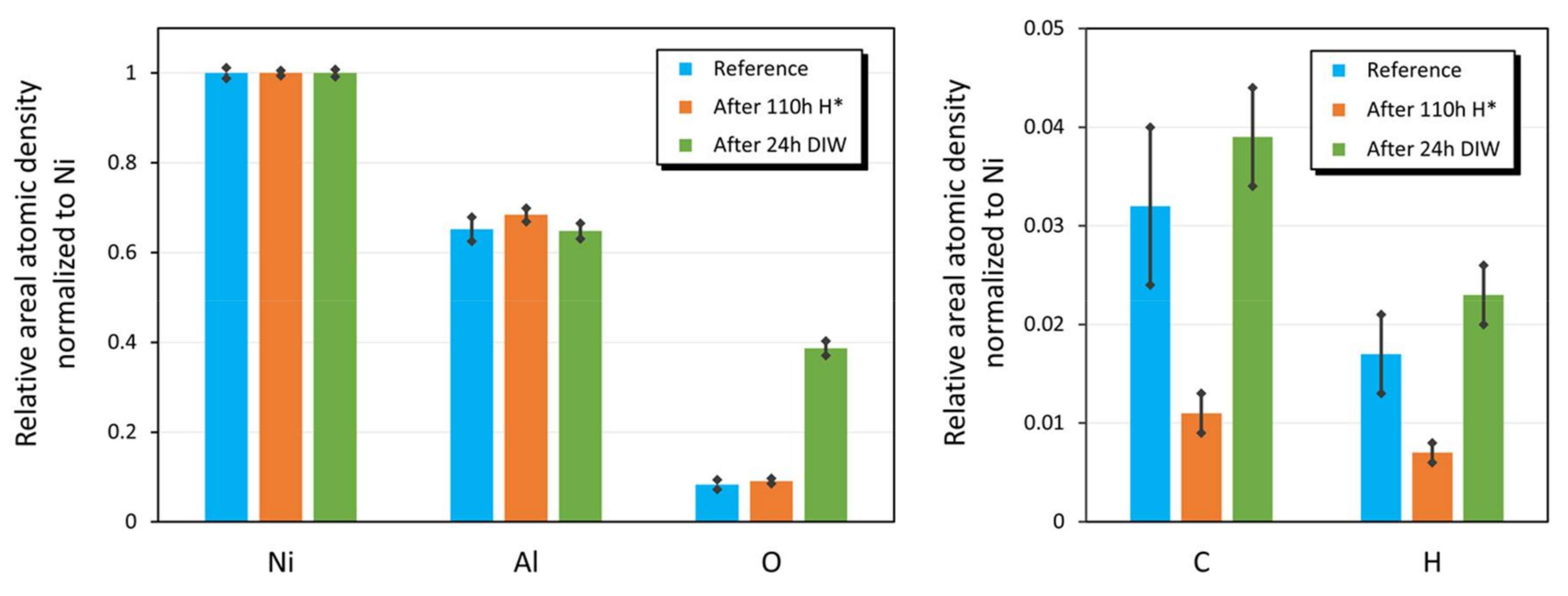
The average composition changes of Ni
3Al are compared between a reference sample, after 110 h H*, and after 24 h DIW. The basic cleaning condition with NH
4OH was disregarded, as Al was not stable under this condition. Ion beam characterization techniques, such as RBS and ERDA, are very sensitive to changes in elemental composition. These techniques were used to measure Ni and Al areal atomic density. As Ni was expected to be stable under the conditions of the durability tests [
13,
45], the Ni areal atomic density was used for normalization. The relative atomic density of Ni, Al, O, C and H, are presented in
Figure 7.
The Ni:Al ratio remained around 3:2. Though, a significant increase in oxygen content is observed after 24 h in DIW, which is consistent with the Pourbaix diagram. Likely, more O-bonds has been formed, resulting in increased roughness, yet without changing the total thickness as the XRR oscillation frequency did not increase. Furthermore, traces of C and H are clearly reduced after H* exposure, which is not unexpected as H* is used in mask cleaning processes to reduce organic contamination. Note that traces of C and H have not been reduced after DIW cleaning procedure.
We have conducted durability tests on Ni3Al. The behavior of NiAl and Ni2Al3 are expected to be like Ni3Al, as all three samples exhibit the same native oxide. The surface Al oxide dissolves in NH4OH, but remains stable in DIW, though metallic Al will be further oxidized and might increase roughness. The Ni:Al ratio remained the same after DIW submersion and after H* tests, indicating neither preferential dissolution nor preferential sputtering has occurred respectively. To be compatible with more basic conditions, a cleaning solution with high Al3+/AlO2− concentration can increase the passivation region. Alternatively, a capping layer can limit the exposure of the surface Al to the surroundings, thereby limiting oxidation. Another option is to saturate all Al-O bonds during deposition, while aiming for low surface roughness. This way, the roughness remains low as no further oxidation will occur during cleaning under passivation conditions.
3.3. Composition and Density Profile
The composition and density of the absorber material is needed to estimate its theoretical optical constants by providing the weight percentage wj and alloy density ρalloy in Equation (1) respectively. Many metals form a native surface oxide layer as well, which will be determined with XPS and TEM-EDS. The composition and density of both surface oxide and bulk layer can be determined by fitting XRR measurements.
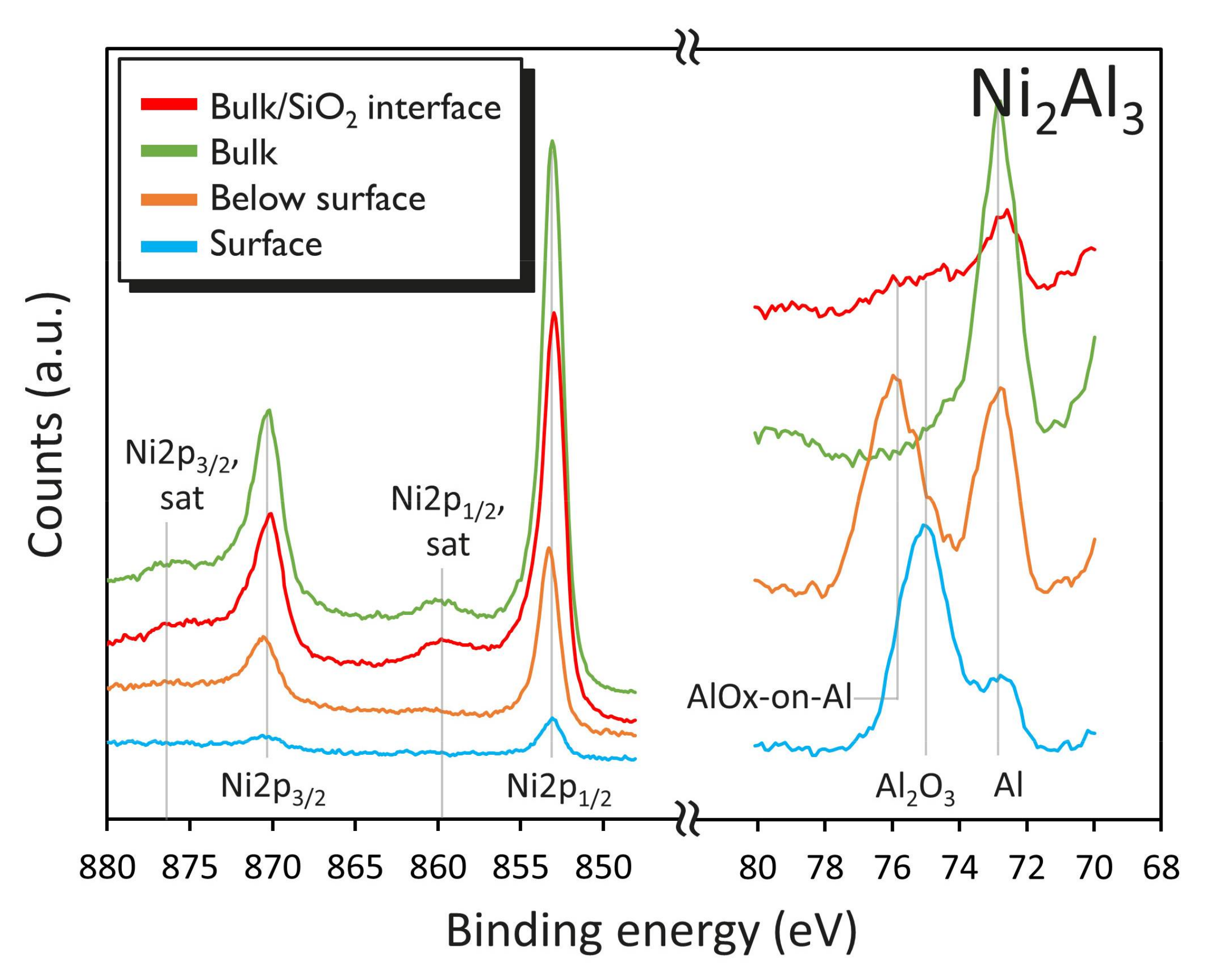
XPS is an effective technique to determine the oxidation state on the surface, which provides information on whether the atom is bound in a compound, or whether it is in pure metallic state. Depth profile can be obtained in sputter-assisted mode. XPS measurement of Ni
2Al
3 is presented in
Figure 8. XPS data for Ni
3Al and NiAl are available in the
Supplementary Materials section Figure S1.
Ni2p3/2, and Ni2p1/2 peaks are found at 852.7 eV, and 870.0 eV respectively. On the surface, there is a negligible amount of Ni present. The peak positions inside the bulk of the film correspond to metallic Ni. In case Ni was in a compound, the Ni2p3/2 and Ni2p1/2 peaks will shift slightly to higher binding energy around 854.4 eV and 871.9 eV respectively, possibly splitting in multiplet peaks and having more pronounced satellite peaks.
Al2p peak is observable at 72.6 eV, 74.6 eV and 75.6 eV for metallic Al, Al2O3 and AlOx-on-Al respectively. On the surface (0 s sputter time), a main Al2O3 peak with a side metallic Al peak can be discerned. Just below the surface (100 s sputter time), the Al2O3 peak shifts to higher binding energy, corresponding to Al suboxide-on-Al, while the metallic Al peak becomes more dominant. In the bulk (up to 1300 s sputter time), the main peak is metallic Al with a small sidelobe at higher binding energy, indicating the presence of some Al suboxide.
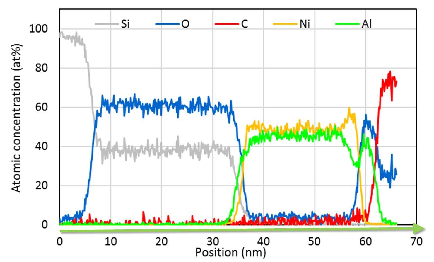
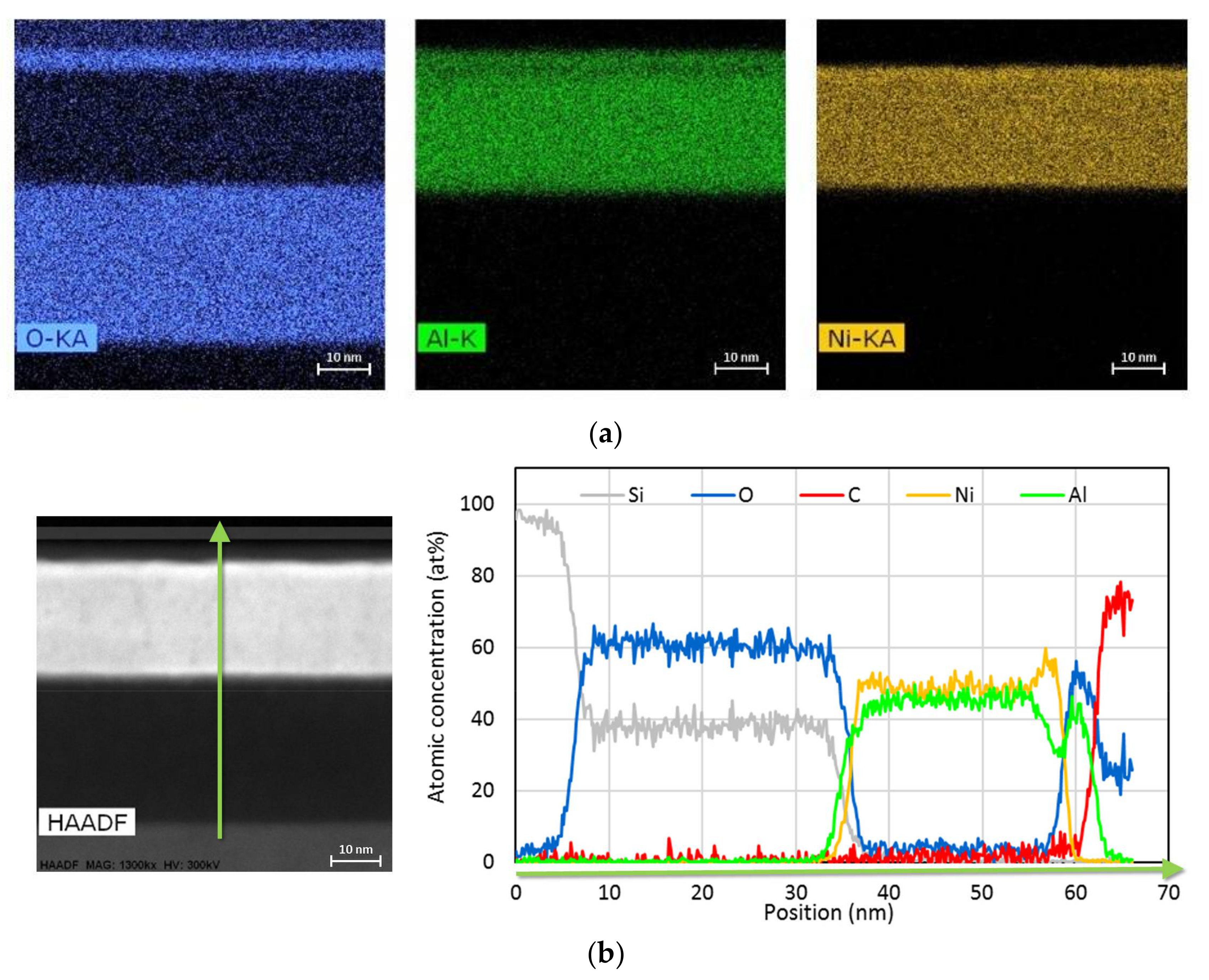
TEM-EDS image of Ni
2Al
3, illustrated in
Figure 9, confirms that the native oxide is composed out of Al and O. Ni is confined within the bulk, which also contains Al and traces of O. The bulk composition therefore has changed compared to nominal. All elements within the bulk metal layer seem to be uniformly distributed. TEM-EDS line scan reveals preferential Al diffusion towards high oxygen concentration, such as at the surface and at the SiO
2 interface. This leaves a Ni-rich layer just below the native oxide and on top of SiO
2. The Al:O ratio is not stoichiometric 2:3 beneath the surface, indicating formation of sub-oxides where less than the maximum number of Al-O bonds were formed.
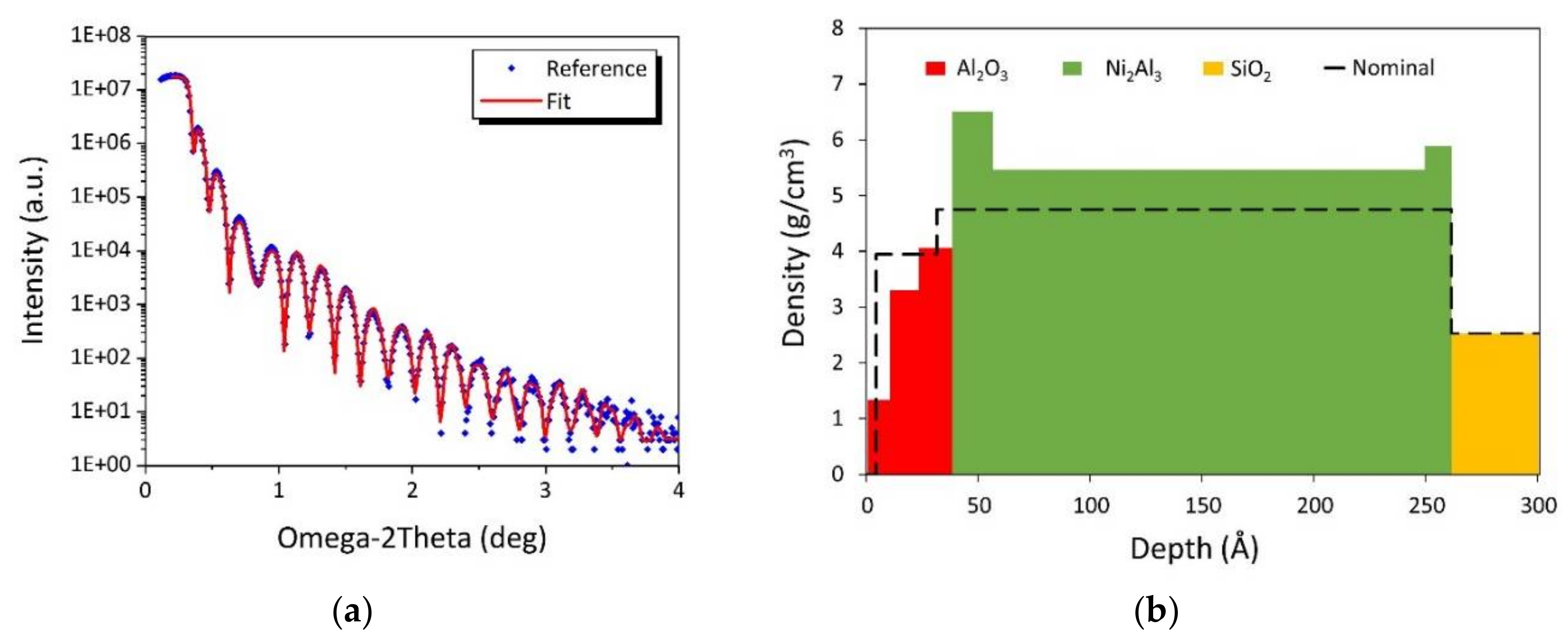
Figure 10 presents the XRR spectra of Ni
2Al
3. The measurements for the other samples can be found in the
Supplementary Materials section Figure S2. A multilayered model was used to account for density gradients, with layer thickness, density and roughness as fitting parameters. The nominal line follows the crystalline density of Al
2O
3 and Ni
2Al
3 along the layer thickness measured from TEM images. The density of the largest bulk layer is considered the bulk density of the film, and is tabulated in
Table 4.
The density calculated with XRR, can differ from crystalline density from literature, due to non-optimized packing order or due to dissimilar bulk composition from nominal, as some Al diffuses away from bulk to form the native oxide. Two peaks are observable in the Ni2Al3 density profile: just below the surface oxide and on top of SiO2 substrate, corresponding to the Ni-rich layers where Al has diffused away.
The bulk composition can be calculated from bulk density using the rule of mixtures for the mass density of alloy composites, with
wi and
ρi the weight percentage in the alloy and density of the
i’th element respectively:
Only Ni and Al were considered for composition determination without taking into account the O content. The calculated bulk composition of Ni
3Al and NiAl are very similar, around 3:1 Ni:Al ratio. Although the NiAl sample contains relatively more Al than Ni
3Al, more Al has diffused away towards the surface, resulting in a thicker surface oxide layer in the NiAl sample (cf.
Figure 4) and a higher Ni content in the bulk compared to nominal composition. Similarly, the bulk composition of Ni
2Al
3 ends up closer to 1:1 Ni:Al ratio.
With the bulk alloy density ρalloy and the bulk composition wj from XRR spectra, we can proceed to calculate the optical constants n,κ with the Equation (1).
4. Verification of Optical Constants
In this section, we compare optical constants, calculated by Equation (1) with values from film characterization in
Section 3, and by fitting EUVR measurement. The optical constants will be used in rigorous simulations to predict M3D impact in
Section 5.
The first set of
n,
κ is calculated using crystalline density and composition of Ni
xAl
y compounds from literature. The second set of optical constants is calculated based on bulk density and bulk composition obtained with XRR. These density and composition values are tabulated in
Table 4. The third set of optical constants are calculated from fitting EUVR data, which were collected with PTB’s soft X-ray radiometry beamline at BESSY II facility. The EUV reflectance of Ni
3Al, NiAl and Ni
2Al
3 was measured through wavelength and through incidence angle. The results have previously been reported in [
50]. We fit the measured EUV reflectance with a three-layer stack model, consisting out of native oxide, bulk metal, and SiO
2 on Si-substrate. The fitting parameters consist out of layer thickness, and optical constants. The EUV reflectance fits are illustrated in the
Supplementary Materials Figure S3; the resulting optical constants at 13.5 nm wavelength are tabulated
Table 5.
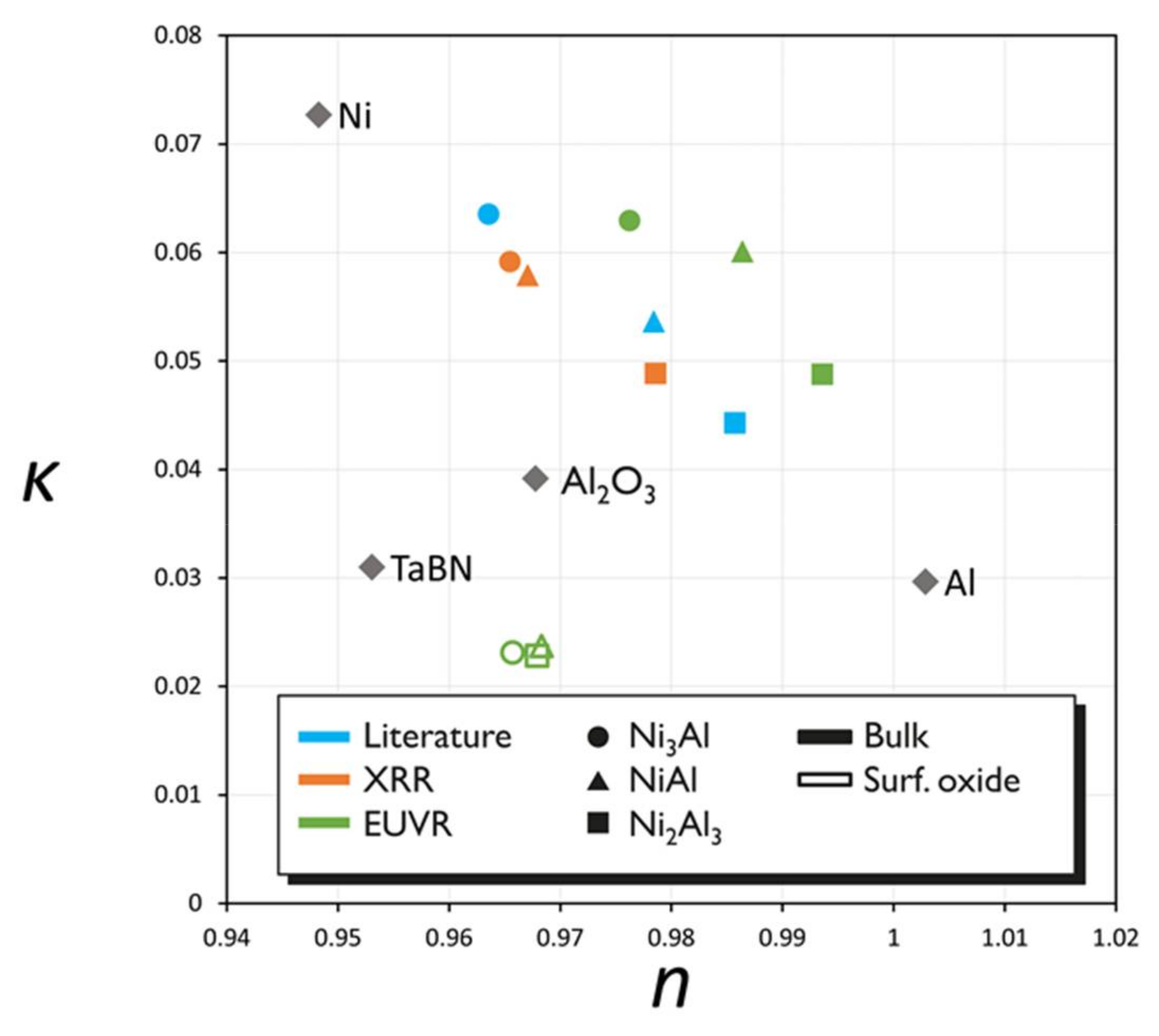
Figure 11 compares the optical constants obtained through literature, XRR, and EUVR.
EUV reflectance shows higher κ with increasing Ni content and n closer to unity with increasing Al content. The extinction coefficients κ are very comparable between calculation based on literature, XRR, and EUVR.
However, EUVR found the refractive coefficients
n much closer to unity. The calculated optical constants of the Ni
xAl
y compounds lie linearly between those from the single elements Ni and Al, and is based on their tabulated atomic scattering factor f
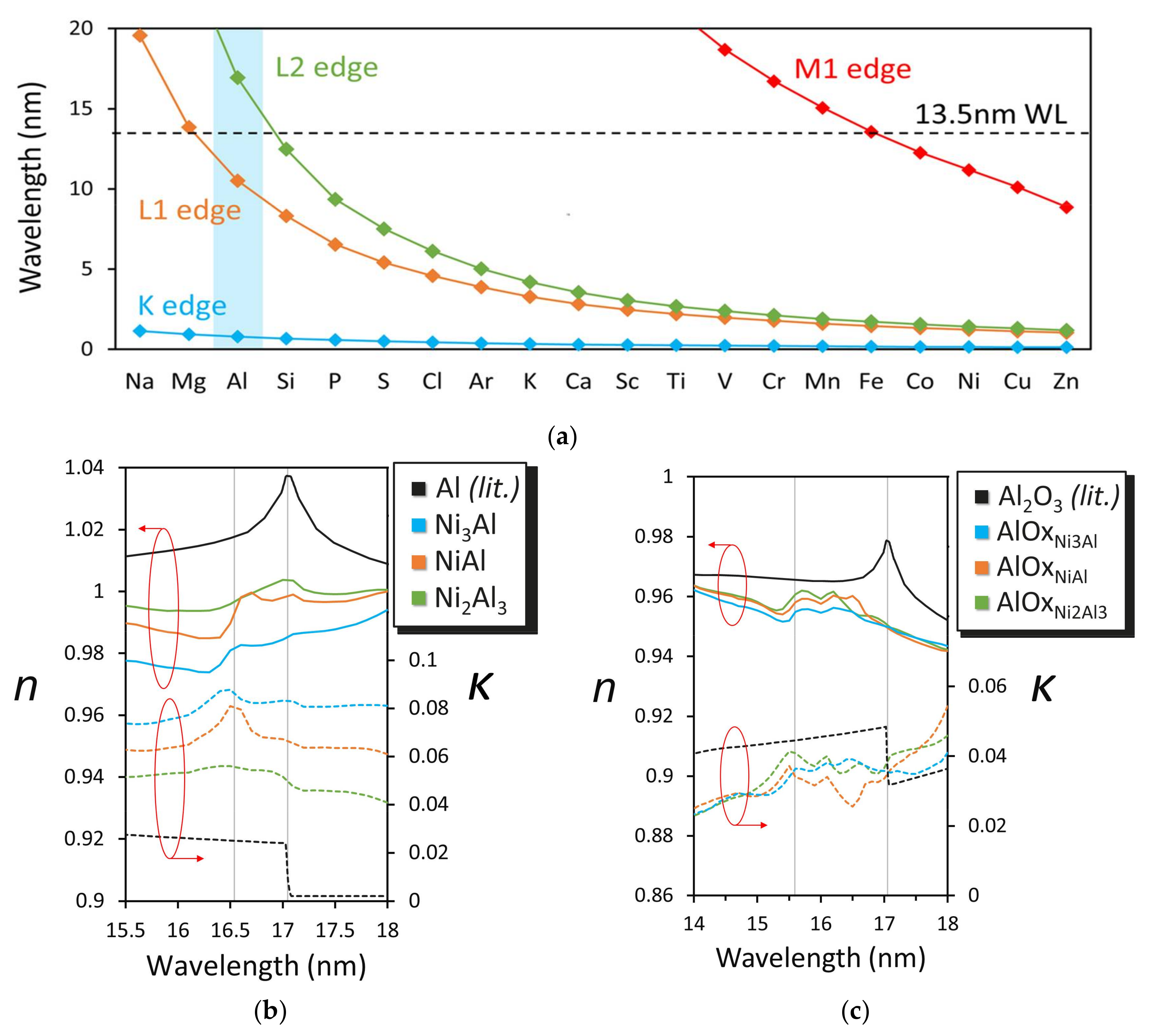
i, which is very sensitive to absorption edges. Depending on the chemical state of the element, the absorption edge can shift through wavelength, resulting in different optical constants. Few elements have absorption edges near 13.5 nm EUV wavelength, one of which is Al. Metallic Al L2 absorption edge lies at 73.1 eV [
51], corresponding to a wavelength of ~17 nm, as illustrated in
Figure 12a.
XPS measurements showed partially oxidized Al at the surface and in the bulk (cf.
Figure 8). Higher binding energy of Al-O bonds compared to Al-Al, will shift the Al L2 edge towards higher energy and smaller wavelength. To verify this behavior, additional EUV reflectance was measured between 16 nm and 18 nm wavelength to determine the Al L2 absorption edge position.
Figure 12b reveals a shift of Al L2 absorption edge from theoretical position at 17 nm to 16.6 nm wavelength. Close to the absorption edge, the refractive coefficient
n of Al varies strongly with the wavelength, therefore the oxidation-induced absorption edge shift significantly impacts the value of
n for the Ni
xAl
y alloys at 13.5 nm wavelength. The positive
n-over-wavelength gradient moves the value of
n closer to unity after shifting the absorption edge.
The fitted optical constants of the Al
2O
3 native oxide are similar across the Ni
xAl
y samples, suggesting there is almost no variation in native oxide composition and density. From
Figure 12c, we can observe the Al L2 absorption peak has shifted further towards 15.5 nm, as there are more Al-O bonds in the surface oxide compared to bulk.
Figure 11 shows a much smaller
κ for the native surface oxide as measured by EUVR, compared to literature values for crystalline Al
2O
3. The
κ reduction is caused by a partial oxidation of the surface layer, resulting in a lower Al
2O
3 density as compared to crystalline Al
2O
3. The partial oxidation is corroborated by XPS, and TEM; the reduced density by XRR measurements (cf.
Figure 8,
Figure 9 and
Figure 10). A lower density would also result in larger
n, yet its value is comparable between EUVR measurement and literature. This can be explained by a combination of the Al L2 absorption edge shift, a slightly negative
n-over-wavelength gradient of Al
2O
3, and atypical orbital-atom interactions.
Up to this point, we have presented experimental characterization results, leading up to the determination of realistic NixAly optical constants with EUVR. In the next section, the measured optical constants will be incorporated in an absorber mask model to simulate and predict the impact on imaging of the NixAly alloys.
5. EUV Imaging Simulations
In this section, we utilize the optical constants, as measured by EUVR and tabulated in
Table 5, to predict M3D impact of Ni
xAl
y mask absorbers, compared to current TaBN absorber and high
κ single metal Ni absorber.
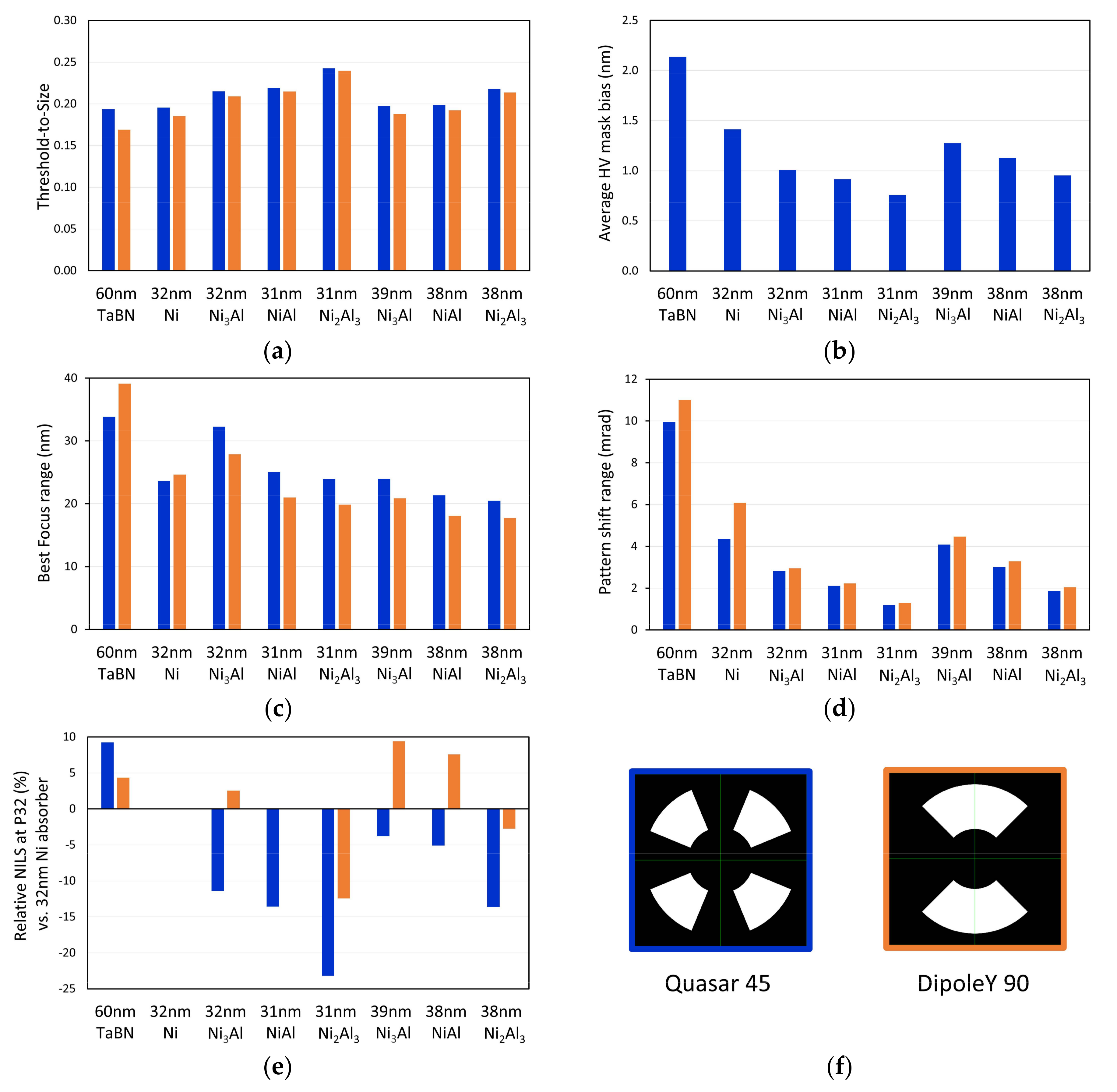
We used Synopsys Sentaurus Lithography software to assess intensity threshold-to-size, shadowing effects, best focus shift through pitch, pattern shift through focus, contrast and process window (PW) variation of dense-to-isolated trenches at a fixed CD of 16 nm, which is a relevant structure for the 7 nm technology node. The simulated illumination source shapes are DipoleY with 90° opening angle and Quasar with 45° opening angle at numerical aperture (NA) of 0.33.
The imaging impact of the Ni
xAl
y absorbers is compared to the reference 60 nm TaBN absorber, and a 32 nm high
κ Ni absorber [
9]. The EUV reflective mirror is a calibrated model of an experimentally validated Mo/Si ML mirror capped with Ru [
52]. The Ni
xAl
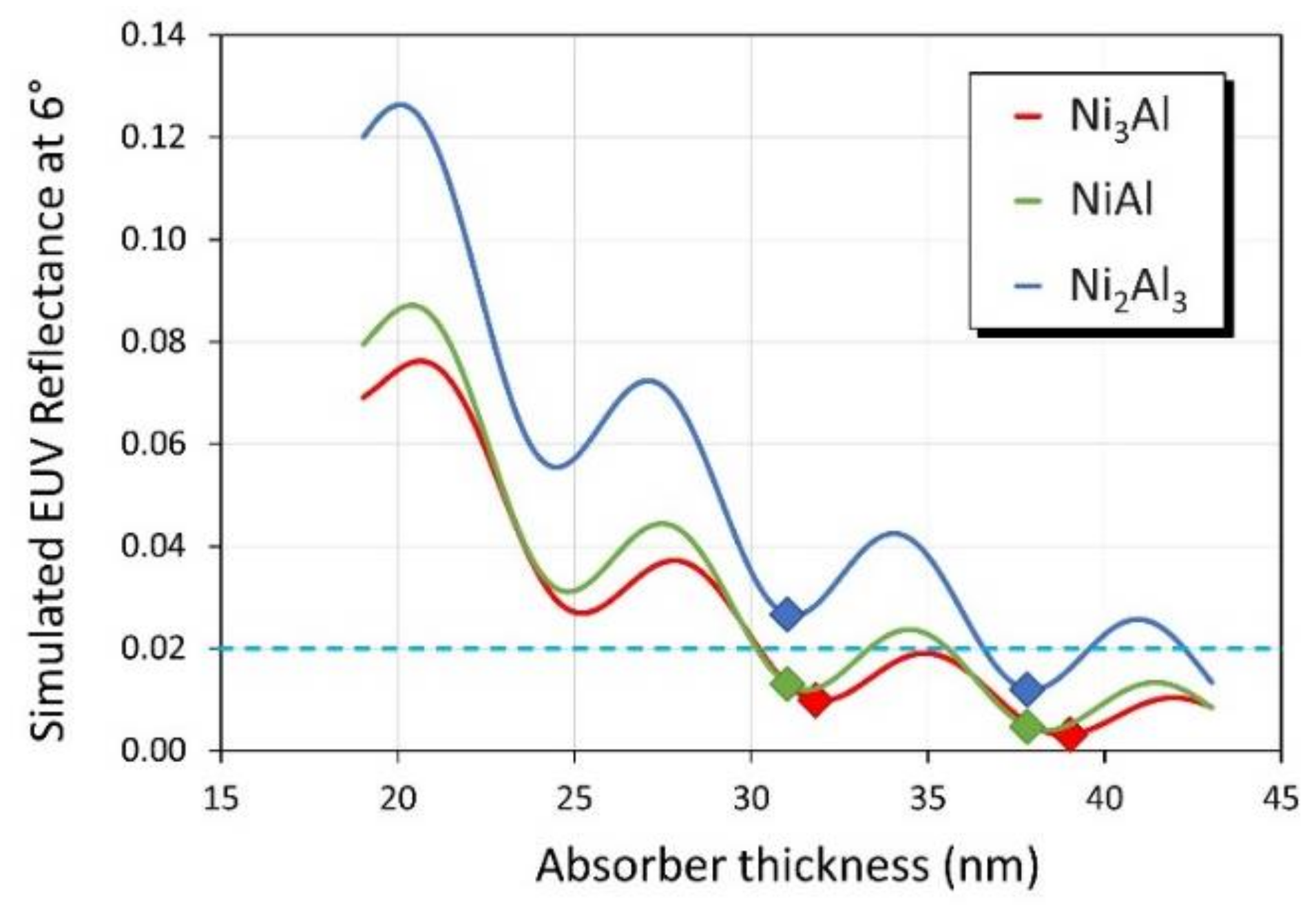
y absorber models contains two layers: a surface oxide layer with fixed 3 nm thickness and a bulk metal absorber layer. The optimal thickness is selected at an EUV reflectance minimum below 2%, as depicted in
Figure 13. The optical constants are tabulated in
Table 5.
The exposure dose needed to print the patterns on target, is estimated by the intensity threshold-to-size, with high threshold corresponding to low dose.
Figure 14a predicts higher threshold-to-size for thin Ni
xAl
y absorbers, and for high Al-content absorbers. As expected, thinner absorbers and Al low
κ result in less EUV dose required to print trenches on target.
Impact on shadowing effect under the Quasar illumination is depicted in
Figure 14b as the mask CD difference between horizontal (H) versus vertical (V) patterns, which are biased to print on target at wafer level. All Ni
xAl
y absorbers have smaller HV mask bias compared to reference TaBN and to the thin high
κ Ni absorber, despite being physically thicker. Higher Al content further reduces HV mask bias. This signifies that shadowing effect is not purely a thickness-induced M3D effect, but is also impacted by phase deformation.
The best focus range from 32 nm to 100 nm trench pitch is shown in
Figure 14c. The smaller best focus shift between different pitches is better for overlay. Most Ni
xAl
y absorbers exhibit slight reduction in best focus range compared to thin high
κ Ni absorber, with more reduction at higher Al-content. More Al leads to smaller phase deformation as the refractive coefficient
n is closer to unity. The thicker Ni
xAl
y absorbers have smaller best focus range, as the impact of phase deformation on best focus shift is reduced for darker absorbers with lower reflectance [
2].
Figure 14d illustrates the range of pattern shifts through focus for pitches from 32 nm to 100 nm, expressed in milliradians (mrad). 10 mrad correspond to 1 nm pattern shift per 100 nm defocus. Thinner absorbers are preferable as they reduce the contribution of absorber shadowing to pattern shift through focus, as it causes an imbalance in the diffraction orders intensity [
5]. Furthermore, with
n is close to unity due to Al, there is less phase imbalance between illumination poles under off-axis illumination [
6]. Imaging simulations predict all modeled Ni
xAl
y absorbers to surpass TaBN and Ni in mitigating pattern shift through focus.
The contrast is expressed in normalized intensity log-slope (NILS), with better contrast with higher NILS. In
Figure 14e NILS of the Ni absorber at 32 nm pitch is chosen as reference for each illumination. For the Quasar illumination, TaBN absorber exhibits the best NILS, outperforming all Ni
xAl
y absorbers. However, with the DipoleY illumination, which is superior for small patterns, 39 nm Ni
3Al and 38 nm NiAl absorbers exceed both TaBN and Ni absorbers in NILS.
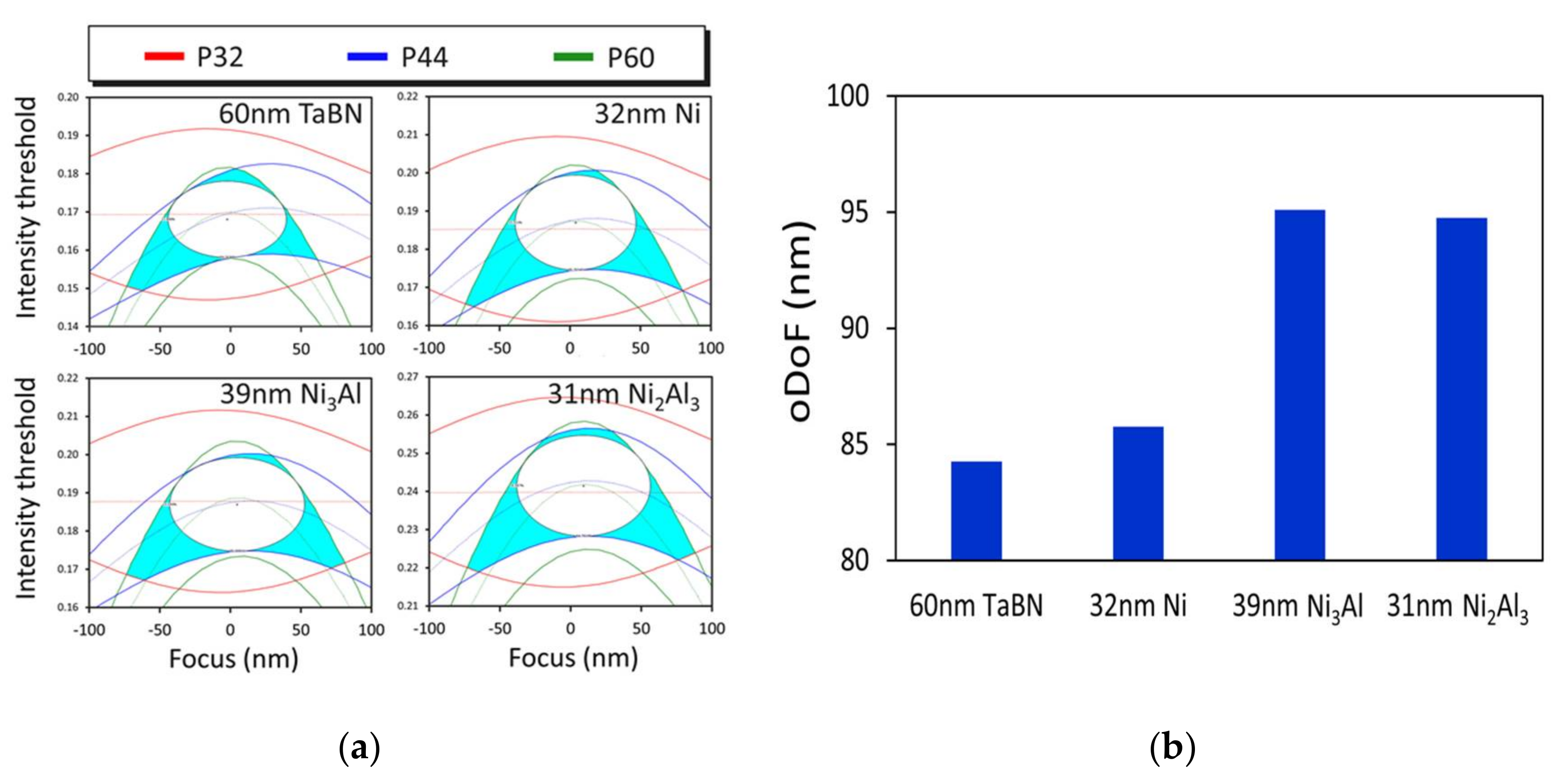
Lastly, the overlapping process windows under the DipoleY illumination at 0.33 NA are compared between 60 nm TaBN, 32 nm Ni, 39 nm Ni
3Al—as the Ni
xAl
y stack with best NILS, and 31 nm Ni
2Al
3—as the Ni
xAl
y stack with best M3D reduction. These process windows are determined as the range of exposure dose and focus in which a 16 nm trench line/space pattern varies ±10% from target CD. Mask bias has been applied for each pitch, as to print the trenches on target CD at the specified exposure. The overlap of process windows (oPW) for pitch 32 nm, 44 nm and 60 nm, are shown in
Figure 15.
The oPW of Ni, Ni3Al, and Ni2Al3 are larger comparing to TaBN. The smallest best focus shift is recognized as the most symmetric oPW, which is the case for the Ni2Al3 absorber. The overlapping depth-of-focus (oDoF) has increased more than 10% for the Al containing absorbers, compared to the TaBN and the Ni absorber. Ni3Al has a similar oDoF compared to Ni2Al, but is more preferred for its higher NILS.
In conclusion, based on rigorous EUV imaging simulations, there is a trade-off between phase distortion reduction, and NILS. High Al-content alloys are expected to exhibit significant contrast loss, despite superior phase distortion reduction, especially at reduced absorber thickness. A 39 nm Ni3Al turns out to be the best candidate out of the simulated absorber models, with superior M3D mitigation combined with high NILS under DipoleY illumination, when compared to 60 nm TaBN and 32 nm Ni absorbers.
6. Discussion and Outlook
In this paper, we present an extensive experimental methodology flow to evaluate candidate absorber materials capable of reducing M3D effects. We have started characterizing alloys to a list of specifications, including film morphology, durability under cleaning conditions, and under hydrogen conditions. The optical specification for absorber materials for BIM require high extinction coefficient κ and refractive coefficient n close to unity. Before determining the optical constants, the film profile needs to be characterized first with sufficient depth resolution, especially in the case when more than a single layer is formed after deposition. Accurate measurement of the film profile is used to set up an absorber model with improved fitting convergence of the EUV reflectance data, and from which realistic optical constants can be precisely extracted.
Three nominal compositions of the Ni-Al system have been investigated with various material and optical characterization techniques.
Alloying Ni and Al was unable to remove crystallinity completely, but the Ni-Al crystal grain size has decreased compared to pure Ni crystal grains. The as-deposited Ni2Al3 alloy shows nano-crystallinity morphology, but recrystallizes above 200 °C. As-deposited NiAl and Ni3Al exhibit poly-crystallinity and retain this morphology at higher temperatures.
A native Al2O3 layer forms naturally on the NixAly alloy surface when Al is exposed to atmospheric oxygen. The surface oxide grows with increasing Al-content. A chemical stable capping layer can possibly protect Al from oxidizing. Alternatively, saturating all Al-O bonds resulting in a uniform Al2O3 composition, can ensure the absorber composition does not change over time.
EUVR verified higher κ with increased Ni content and n closer to unity with increased Al content. Measurement through wavelength detected Al L2 absorption edge shift towards 16.6 nm wavelength, resulting from Al oxidation in the NixAly material. This near-edge anomalous scattering behavior causes the refractive coefficient n to be much closer to unity at 13.5 nm wavelength, which can be advantageous for BIM absorbers.
Lithography imaging simulations predict a trade-off between better phase distortion reduction for high Al-content alloys, and higher contrast for high Ni-content alloys. Nevertheless, higher EUV absorption compared to 60 nm TaBN, allows the NixAly absorbers to be thinner, resulting in lower dose-to-size, less shadowing effect, less pattern shift through focus, smaller best focus shift range, and larger overlapping process windows. Taking contrast loss into consideration, the best candidate out of the simulated absorber models is a 39 nm Ni3Al absorber stack.
Although Ni etch is still challenging, promising mitigation strategies to overcome the issues of Ni in respect to etch and repair are under investigation. We have demonstrated that Ni-Al alloys are worthwhile candidates for mask absorber material with good imaging and mask life time expectations. The presented extensive evaluation of Ni-Al alloys is encouraging to increase the efforts in promising patterning strategies for magnetic metals.

 ,
, 


