Article

Trade-off between Photon Management Efficacy and Material Quality in Thin-Film Solar Cells on Nanostructured Substrates of High Aspect Ratio Structures

1
nLiten Energy Corporation, 650 Castro Street, Suite 120–422, Mountain View, CA 94041, USA
2
Affiliated with Arizona State University, School of Electrical, Computer, and Energy Engineering, Tempe, AZ 85287, USA
3
Currently with Natron Energy, 3542 Bassett St, Santa Clara, CA 95054, USA
4
National Renewable Energy Laboratory, 15013 Denver West Parkway, Golden, CO 80401, USA
5
Currently with Jinko Solar, 595 Market Street, Suite 2200, San Francisco, CA 94105, USA
*
Author to whom correspondence should be addressed.
Appl. Sci. 2018, 8(4), 616; https://doi.org/10.3390/app8040616
Submission received: 12 January 2018 / Revised: 14 February 2018 / Accepted: 18 February 2018 / Published: 13 April 2018
(This article belongs to the Special Issue Nanostructured Photodetectors and Photovoltaic Devices)

Abstract

:
Although texturing of the transparent electrode of thin-film solar cells has long been used to enhance light absorption via light trapping, such texturing has involved low aspect ratio features. With the recent development of nanotechnology, nanostructured substrates enable improved light trapping and enhanced optical absorption via resonances, a process known as photon management, in thin-film solar cells. Despite the progress made in the development of photon management in thin-film solar cells using nanostructures substrates, the structural integrity of the thin-film solar cells deposited onto such nanostructured substrates is rarely considered. Here, we report the observation of the reduction in the open circuit voltage of amorphous silicon solar cells deposited onto a nanostructured substrate with increasing areal number density of high aspect ratio structures. For a nanostructured substrate with the areal number density of such nanostructures increasing in correlation with the distance from one edge of the substrate, a correlation between the open circuit voltage reduction and the increase of the areal number density of high aspect ratio nanostructures of the front electrode of the small-size amorphous silicon solar cells deposited onto different regions of the substrate with graded nanostructure density indicates the effect of the surface morphology on the material quality, i.e., a trade-off between photon management efficacy and material quality. This observed trade-off highlights the importance of optimizing the morphology of the nanostructured substrate to ensure conformal deposition of the thin-film solar cell.

1. Introduction

Although texturing of the transparent electrode of thin-film solar cells (particularly amorphous silicon solar cells) has long been used to enhance light absorption (and thus the conversion efficiency) via light trapping, such texturing has involved low roughness (i.e., structures with heights less than 100 nm) and thus is limited regarding the degree of light absorption enhancement that is possible in thin-film solar cells (see, e.g., Reference [1]). With the recent developments in nanotechnology, a new approach called photon (light) management [2,3,4,5,6,7] in thin-film solar cells has been developed to further enhance the light absorption in thin-film solar cells; the ultimate goal is to enable even thinner films to be used while still providing higher conversion efficiency. Of the wide variety of approaches to perform photon management in thin-film solar cells, one particularly attractive approach is the use of nanostructured substrates with an array of nanostructures of high aspect ratio that have greater height from the substrate; such a nanostructured morphology manifests itself in the subsequently deposited thin-film solar cell, thereby allowing improved optical absorption [2,3,4,5,6,7,8]. The higher aspect ratio structures that can be produced are particularly advantageous for enhancing the light absorption in thin-film solar cells with very thin absorber layers, e.g., amorphous silicon (a-Si) solar cells deposited onto a nanostructured substrate comprised of an array of nanopillars (see e.g., [5]). Because of the “folded” morphology of the subsequently deposited thin-film solar cell on the nanostructured substrate, typically based on a p-n or p-i-n junction semiconductor device, we refer to such a device as a “folded junction” solar cell [2,3,4].
Despite the great progress in the development of photon management in thin-film solar cells using nanostructured substrates, most of the studies on the use of nanostructured substrates focus on the improvement in optical absorption in folded junction solar cells and do not consider the effect of reduced material quality of thin-film solar cells deposited on such nanostructured substrates. Understanding the relationship between material quality and nanostructured morphology is crucial for practical implementation of nanostructured substrates in thin-film solar cells.
Here, we report the observation of a correlation between the reduction of the open circuit voltage (related to the degradation of the material quality) of a-Si thin-film solar cells and the areal number density of high aspect ratio structures of the front contact (i.e., transparent conducting electrode of the solar cells in the superstrate configuration) of each solar cell. As discussed above, the high aspect ratio nanostructures enable enhanced light absorption in the folded junction solar cells via improved photon management; as a result, a higher areal density of such nanostructures corresponds to an overall increase in the light absorbed by the folded junction solar cell. However, the enhanced light absorption does not necessarily correspond to enhanced conversion efficiency, particularly if the material quality of the absorber layer is degraded [9]. Thus, we report a trade-off between photon management efficacy and material quality in a-Si folded junction solar cells. The results highlight the importance of considering the material quality of the absorber layer of thin-film solar cells deposited onto nanostructured substrates.

2. Materials and Methods

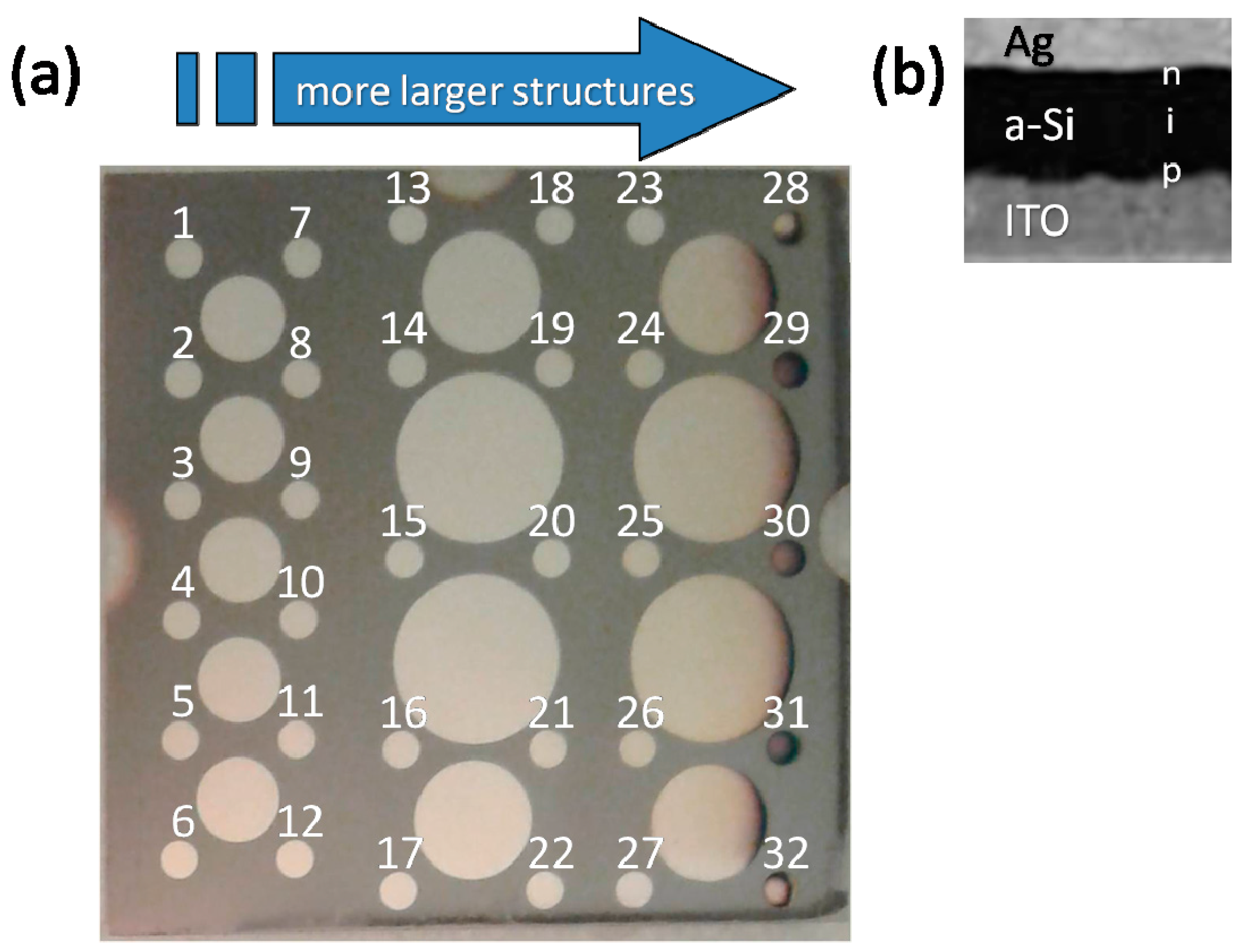
Amorphous silicon solar cells were deposited onto various nanostructured substrates at the National Renewable Energy Laboratory (NREL). Although a variety of nanostructured substrates were considered, one in particular had a spatial gradient of areal density of higher aspect ratio nanostructures, which allowed for the convenient study of the effect of the morphology of the nanostructured substrate on the a-Si solar cell device performance (and thus on the material quality).
Zinc oxide nanostructures were deposited onto indium tin oxide (ITO)-coated glass substrates using an electrochemical deposition method that is similar to the method described in a patent [3] and a patent application [4] of nLiten Energy Corporation, but with the application of an electrical bias. A brief description of the method is provided here.
All chemicals used in the zinc oxide nanostructure growth process were obtained from Sigma Aldrich. The growth solution was prepared by dissolving zinc nitrate (0.001 M), hexamethylene tetramine (0.001 M), and polyethyleneimine (0.03 M) in deionized water. The pH of the solution was adjusted to 10.5, and then the solution was heated to 80 °C. For each sample, a piece of ITO-coated glass (2” × 2”) was used as the working electrode (upon which the zinc oxide nanostructures were deposited), a zinc foil (2” × 2”) was used as the counter electrode, and a Saturated Calomel Electrode (SCE) was used as the reference electrode. The distance between the working electrode and the counter electrode was 2 cm. The electrochemical deposition was performed at −1.0 V for different times, depending on the average size of the nanostructures desired. For the substrate with graded areal density of larger nanostructures described below, the deposition time was 10 min. Our hypothesis is that the short deposition time and the resistance of the ITO (reduced applied voltage further from the wire contact to the ITO substrate) resulted in a gradient in the areal density of larger nanostructures, i.e., for the short deposition time, incomplete growth resulted in a gradient in the number of high aspect ratio nanostructures on a substrate, with a lower number of larger nanostructures further away from the edge of the substrate where the voltage is applied. Finally, the coated substrate was withdrawn from the solution and then rinsed, first with deionized water, and then with methanol.
Prior to deposition of amorphous silicon thin-film solar cells, a 250 nm layer of ITO was deposited on top of the nanostructured substrate to ensure the conductivity of the nanostructured layer is high enough for efficient carrier extraction. Note that this layer is not thick enough to passivate all “structural defects”, as will be discussed below [2].
The a-Si:H solar cells with p-i-n structure (superstrate configuration) produced at NREL were deposited on ITO coated glass by plasma-enhanced chemical vapor deposition (PECVD) using a RF power of 13.56 MHz in a multi-chamber cluster tool (MVSystems, Inc., Arvada, CO, USA) at a substrate temperature of approximately 200 °C. The p-layer (~8 nm) with ETauc of 2.1 eV and dark conductivity of 5 × 10⁻⁴ S/cm was grown using SiH4, BF3, and H2 in the PECVD chamber. The i-layer (~500 nm) with ETauc of 1.78 eV and dark conductivity of 2 × 10⁻¹⁰ S/cm was grown using SiH4 without hydrogen dilution in the PECVD chamber. The n-layer (~20 nm) with ETauc of 1.75 eV and dark conductivity of 2 × 10⁻² S/cm was grown using a SiH4 and PH3/H2 mixture in the PECVD chamber. Finally, various Ag dots with masked areas ranging from 0.2 to 0.8 cm2 were deposited using an e-beam evaporator with a shadow mask to define the Ag back electrode layer of separate devices, as shown in the image in Figure 1.
The solar cells were tested using a home-built illuminated current-voltage (I-V) curve tracer probe station coupled to a fiber-coupled Xe lamp light source. Note that, although the spectrum of the light source was not filtered to match the AM 1.5 solar spectrum, because all the solar cells were tested under the same conditions, we can perform a comparative study of the solar cells tested using the illuminated I-V data obtained with this setup.

3. Results

We obtained the solar cell device performance parameters for a variety of devices of the same size (as defined by the Ag back electrode of each device).

3.1. Devices with Different Areal Densities of Nanostructures

The illuminated current-voltage curves for different areal density of larger nanostructures are shown in Figure 2. Note that devices at the same distance from the left edge of the substrate have comparable performance. The corresponding illuminated I-V curve parameters for representative devices of different areal densities of larger nanostructures are listed in Table 1. In Figure 3, the increased areal density of larger nanostructures for these devices is indicated by a corresponding scanning electron microscope (SEM) top-view image of each of the representative devices listed in Table 1. In each SEM image, the larger dome-like features correspond to larger structures, allowing for estimation of the areal density based on the number of larger features for each device over an area of ~850 µm2 (see Table 1).

3.2. Cross-Sectional Image

A focused ion beam (FIB) cross-sectional SEM image of a solar cell similar to that of device 15 of Figure 3 is shown in Figure 4. The FIB cross-sectional SEM image reveals that the nanostructured substrate is predominantly composed of small spheres with regions of larger, higher aspect ratio nanostructures. Note that these larger nanostructures have a height comparable to the thickness of the a-Si solar cell absorber layer and that there is significant deformation of the a-Si layer around such larger nanostructures.

4. Discussion

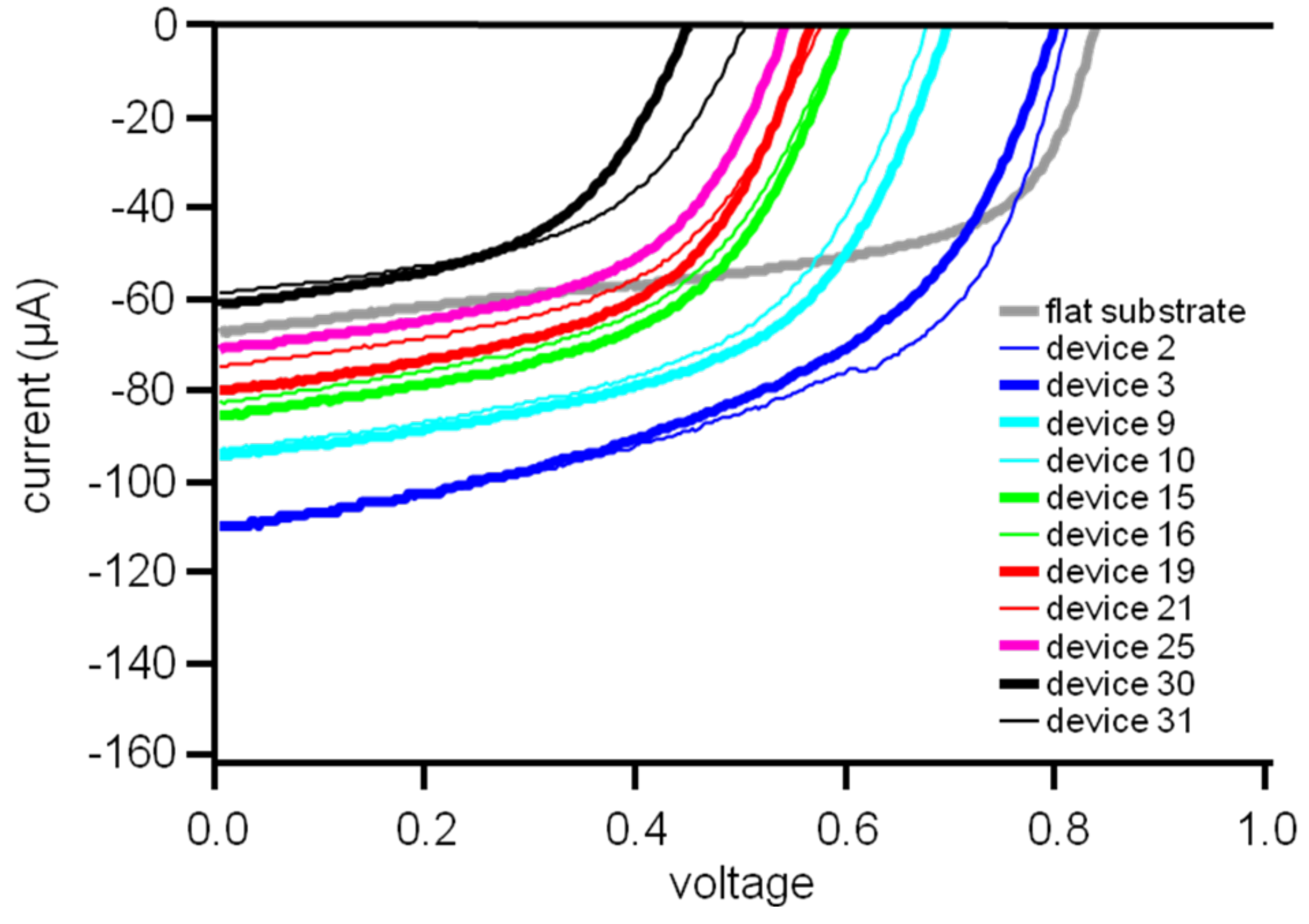
In traditional thin-film solar cells, the degree of surface roughness (i.e., feature height) is small compared to the absorber layer thickness. As a result, the deposition of the absorber layer onto such a surface is approximately the same as the deposition onto a flat substrate. However, when the aspect ratio of the nanostructures on the nanostructured substrate is high (i.e., >1) and the absorber layer thickness is small compared to the nanostructure height (i.e., the “folded junction” configuration of a thin-film solar cell on a nanostructured substrate) the material quality of the absorber layer is a critical issue in the device performance. In the devices considered above with small nanostructures, the aspect ratio of the smaller nanostructures is low (approximately 1) and the height of the smaller nanostructures is small compared to the absorber layer thickness. As a result, the material quality (as indicated by the open circuit voltage of the solar cells) is high for the region of low surface roughness (i.e., primarily smaller nanostructures). However, in the regions with increasing numbers of higher aspect ratio structures for a given area and with height comparable to the absorber layer thickness, the open circuit voltage becomes progressively lower with the increase in areal density of higher aspect ratio structures, i.e., the material quality of the absorber layer becomes progressively worse. Furthermore, the consistent fill factor of all devices suggests that no pinholes exist in the devices, i.e., no shorting occurred. As a result, increased carrier recombination caused by reduced material quality is the primary issue, with carrier recombination increasing with increased areal density of nanostructures, thereby offsetting any enhancements in carrier generation via improved photon management. This reduced material quality is primarily due to the poor conformal coverage of the a-Si layer around the larger nanostructures [8]; such effects are more acute for microcrystalline Si solar cells (see, e.g., [9]). Note that our nanostructures have an added complication of being nonuniform in distribution and orientation. Although such nonuniformities can contribute to the absorber material degradation via inhomogeneity in the absorber layer deposition, the primary cause of the material degradation is the lack of conformal deposition of the absorber material that is further exacerbated with increased aspect ratio of the nanostructures that are substantially oriented perpendicular to the substrate.
A convenient figure of merit to determine whether material quality issues come into play is the relative thickness (absorber layer thickness/nanostructure height) trelative divided by the aspect ratio of the relevant nanostructures on the nanostructured substrate AR, i.e., trelative/AR. If the figure of merit is less than 1 (trelative/AR < 1), then one must consider the effects of deposition onto the nanostructured substrate on the material quality of the absorber layer. The primary effects on the material quality are structural defects caused by poor conformal coverage of the absorber layer. Such defects can be avoided by appropriately tailoring the nanostructures to have a surface that promotes conformal deposition, i.e., no sharp features or sharp corners. Alternatively, a structural buffer layer can be added on top of the nanostructures to smooth/cover any sharp features [2]. Here, as shown in Figure 4, the a-Si absorber layer thickness is approximately 500 nm, the nanostructure height is approximately 500 nm, and the nanostructure aspect ratio is approximately (500 nm)/(250 nm) = 2; as a result, trelative is approximately 1, and the figure of merit is trelative/AR ≈ (1/2) = 0.5. Thus, in the folded junction solar cells considered in this study, trelative/AR < 1 for the high aspect ratio nanostructures.
Note that this discussion does not consider the extreme case of dye-sensitized solar cells, where the ultrathin absorber layer is comprised of molecules deposited in a layer of molecular thickness and thus can conformally cover the nanostructured electrode surface [10]. Here, we consider the case of enhancing the performance of traditional thin-film solar cells using a nanostructured substrate. In addition, note that it is possible to produce high-efficiency devices on nanostructured substrates with trelative/AR < 1; however, such devices require careful design of the nanostructures to enable conformal coverage of the absorber layer (see, e.g., [5]). Alternatively, one can smooth some of the structural defects by depositing a structural buffer layer of appropriate thickness; however, this approach sacrifices some of the enhanced absorption via the reduced aspect ratio nanostructures [2].

5. Conclusions

In the development of thin-film solar cells using nanostructured substrates, one factor that must be considered is how the material quality of the solar cell absorber material is affected by deposition onto a surface with nanostructured morphology via an array of high aspect ratio nanostructures. We found that the a-Si solar cells deposited onto nanostructured substrates with increasing areal density of high aspect ratio nanostructures exhibit a decreasing open circuit voltage caused by the reduction in material quality resulting from poor conformal coverage. We proposed a figure of merit that can be used to indicate whether the material quality may be an issue in a thin-film solar cell using a nanostructured substrate. The use of high aspect ratio nanostructures requires careful consideration of the material quality to fully benefit from the enhancements in photon management provided by such nanostructures.

Acknowledgments

This work was supported by the California Energy Commission (56939A/10-06) and Gary Bjorklund (Bjorklund Family Trust). The authors thank Bill Nemeth of NREL for his help on the deposition of the solar cells. The FIB cross-sectional SEM imaging work was performed at EAG Laboratories.

Author Contributions

Alan H. Chin and Majid Keshavarz conceived and designed the experiments; Alan H. Chin, Majid Keshavarz, and Qi Wang performed the experiments; Alan H. Chin and Majid Keshavarz analyzed the data; Qi Wang performed the amorphous silicon device deposition; Alan H. Chin wrote the manuscript; Alan H. Chin, Majid Keshavarz, and Qi Wang reviewed the manuscript.

Conflicts of Interest

The authors declare no conflict of interest.

References

  1. Sakai, H.; Yoshida, T.; Fujikake, S.; Ichikawa, Y.; Ueda, A.; Ishiwata, O.; Nagano, M. Effects of the surface morphology of transparent electrode on film deposition and photovoltaic performance of a-Si:H solar cells. J. Non-Cryst. Solids 1989, 115, 198–200. [Google Scholar] [CrossRef]
  2. Chin, A.H.; Keshavarz, M.; Wang, G.; Yu, R.; Niu, X.; Yang, L. Light management of tandem solar cells on nanostructured substrates. J. Photonics Energy 2017, 7, 027001. [Google Scholar] [CrossRef]
  3. Chin, A.H.; Keshavarz, M. Thin Film Photovoltaic Devices and Related Manufacturing Methods. China Patent 101990713 B, 5 December 2012. [Google Scholar]
  4. Chin, A.H.; Keshavarz, M. Thin-Film Photovoltaic Devices and Related Manufacturing Methods. U.S. Patent 20090194160 A1, 6 August 2009. [Google Scholar]
  5. Naughton, M.J.; Kempa, K.; Ren, Z.F.; Gao, Y.; Rybczynski, J.; Argenti, N.; Gao, W.; Wang, Y.; Peng, Y.; Naughton, J.R.; et al. Efficient nanocoax-based solar cells. Phys. Stat. Solidi 2010, 4, 181–183. [Google Scholar] [CrossRef]
  6. Wang, K.X.; Yu, Z.; Liu, V.; Cui, Y.; Fan, S. Absorption Enhancement in Ultrathin Crystalline Silicon Solar Cells with Antireflection and Light-Trapping Nanocone Gratings. Nano Lett. 2012, 12, 1616–1619. [Google Scholar] [CrossRef] [PubMed]
  7. Nowak, R.-E.; Geißendörfer, S.; Chakanga, K.; Juilfs, M.; Reininghaus, N.; Vehse, M.; von Maydell, K.; Agert, C. Optimizing Folded Silicon Thin-Film Solar Cells on ZnO Honeycomb Electrodes. IEEE J. Photovolt. 2015, 5, 479–486. [Google Scholar] [CrossRef]
  8. Orhan, J.-B.; Monnard, R.; Vallat-Sauvain, E.; Fesquet, L.; Romang, D.; Multone, X.; Boucher, J.-F.; Steinhauser, J.; Dominé, D.; Cardoso, J.-P.; et al. Nano-textured superstrates for thin film silicon solar cells: Status and industrial challenges. Sol. Energy Mater. Sol. Cells 2015, 140, 344–350. [Google Scholar] [CrossRef]
  9. Python, M.; Madani, O.; Dominé, D.; Meillaud, F.; Vallat-Sauvain, E.; Ballif, C. Influence of the substrate geometrical parameters on microcrystalline silicon growth for thin-film solar cells. Sol. Energy Mater. Sol. Cells 2009, 93, 1714–1720. [Google Scholar] [CrossRef]
  10. Grätzel, M. Dye-sensitized solar cells. J. Photochem. Photobiol. C Photochem. Rev. 2003, 4, 145–153. [Google Scholar] [CrossRef]
Figure 1. (a) Optical image of the a-Si device layout on the nanostructured substrate with graded areal density of high aspect ratio nanostructures (darker shade corresponds to higher areal density); multiple devices (defined by the Ag electrodes of various sizes) are produced on the substrate, with the number besides each approximately 2.5 mm diameter Ag electrode representing the number of the device indicated in Figure 2 and in Table 1 (note that the small devices are locally uniform, with some slight variation in devices 28 to 32 on the right edge of the substrate, where the gradient appears to be the highest). (b) a-Si p-i-n device structure deposited by NREL (see the text for details).
Applsci 08 00616 g001
Figure 2. Illuminated current-voltage curves for different devices shown in Figure 1. Note the similarity in device performance between devices with the same areal density of high aspect ratio nanostructures, i.e., same distance from the left edge of the substrate shown in Figure 1 (e.g., device 2 and device 3). The illuminated I-V curve for a reference device deposited on a flat substrate is shown for comparison.
Applsci 08 00616 g002
Figure 3. Schematic of the correlation between increased light absorption in the a-Si solar cells on the graded nanostructured substrate and reduced open circuit voltage. The background image is the top view of the nanostructured substrate with multiple Ag electrodes of various sizes. Each SEM image inset is a top view of the corresponding device, with the SEM image located at the approximate spatial location of the device on the background image; also included in each inset is the short-circuit current and open circuit voltage of the corresponding device. Note the increased number of larger dome-shaped features for devices on the right side of the substrate, where increased light absorption occurs in the device because of the increased number of high aspect ratio nanostructures and the enhanced light absorption enabled by the nanostructured morphology.
Applsci 08 00616 g003
Figure 4. FIB SEM image of a solar cell similar to device 15 in Figure 3; note that the vertical scale bar is corrected for the viewing angle, i.e., 476 nm (cs) indicates that the actual height of the nanostructure after correcting for the viewing angle is 476 nm. Each high aspect ratio nanostructure (or group of nanostructures) corresponds to a large dome-like feature in the top-view SEM images of the devices (e.g., device 30 has a high number of such high aspect ratio features), and the regions with the smaller nanostructures of lower aspect ratio correspond to the flatter regions in the top SEM images of the devices (e.g., device 3 predominantly has such low aspect ratio features). The scale bar in between the two top-view SEM images on the right is the scale bar for both images.
Applsci 08 00616 g004
Table 1. Representative Device Data.
DeviceEstimated Number of Large Nanostructures in 850 µm2Estimated Areal Density
(µm−2)
Isc
(µA)
Voc
(V)
FFPower (µW)
320.002110.000.800.4942.60
960.00798.000.700.5235.46
15610.07185.500.600.5326.88
19670.07980.500.570.5324.10
25710.08471.090.540.5320.37
30940.1161.470.450.5013.86
Notes: Isc = short circuit current; Voc = open circuit voltage; FF = fill factor.

