Neutralization Dynamics of Slow Highly Charged Ions in 2D Materials
by
 , ,
, ,
Richard A. Wilhelm
1,2,* ,
,
Elisabeth Gruber
1,
Janine Schwestka
1,
René Heller
2,
Stefan Fascko
2 and
Friedrich Aumayr
1 1
Institute of Applied Physics, TU Wien, Wiedner Hauptstr. 8-10/E134, 1040 Vienna, Austria
2
Helmholtz-Zentrum Dresden-Rossendorf, Institute of Ion Beam Physics and Materials Research, Bautzner Landstr. 400, 01328 Dresden, Germany
*
Author to whom correspondence should be addressed.
Appl. Sci. 2018, 8(7), 1050; https://doi.org/10.3390/app8071050
Submission received: 6 June 2018
/
Revised: 22 June 2018
/
Accepted: 23 June 2018
/
Published: 27 June 2018
(This article belongs to the Special Issue Ion Beam Materials)
Abstract
:We review experimental and theoretical work on the interaction of slow highly charged ions with two-dimensional materials. Earlier work in the field is summarized and more recent studies on 1 nm thick amorphous carbon nanomembranes and freestanding single layer graphene by the authors are reviewed. To explain the findings, models for energy loss determination as well as qualitative model descriptions for the observed ultrafast neutralization dynamics are discussed. The results shown in this paper will be put into context with findings of nanostructure formation on two-dimensional materials, both freestanding and on substrate, as well as on surfaces of bulk insulators.
1. Introduction
Interaction studies of slow highly charged ions (HCI) with single atoms, molecules and solids are an active field of basic and applied physics research [1,2,3,4,5]. Many experimental and theoretical studies were performed to understand the neutralization process above the surface and surface modification due to potential energy deposition in the topmost atomic layers [6,7,8,9,10]. While the charge transfer above a surface is well described by the classical-over-barrier (COB) model, the mechanisms at work inside the solid after ion impact, i.e., electron capture, deexcitation processes, and stopping, are still not fully understood. The challenge arises from the fact that ions travelling in a 3D solid will rapidly reach their equilibrium charge state, which is independent of the original charge state and just determined by the ion velocity, limiting the access to the pre-equilibrium regime of the interaction [11,12,13,14].
To gain experimental access to the pre-equilibrium regime, 2D materials come into play as they provide a solid target with only atomic thickness. They allow an experimental observation of phenomena during the pre-equilibrium time in simple beam-foil experiments. Open fundamental questions such as the role which charge state and charge exchange play in slow ion stopping, can now be addressed with the availability of these materials. It may, e.g., be questioned, whether the ion interaction with a 2D solid can be described by extrapolating models derived for 3D solids (thick material) to zero thickness or if qualitatively new phenomena emerge. Additionally, the technological use of ion beams in tailoring optical, electronic, and structural properties of 2D materials for applications such as controlled production of nano-sieves needed in DNA sequencing [15] or adjusting the p- and n-type doping for solar cell applications [16,17] is a major motivation of the work. The deliberate production of defects, the direct implantation of ions, and the perforation of the material will determine the 2D material’s mechanical, optical, and electronic properties.
Here, we review recent work on HCI irradiation of 2D materials, which is a young subfield of ion–solid interaction. As there exists only a limited body of research and many groups are currently joining the field, we focus mainly on our own work over the last five years [2,18,19,20,21,22,23,24] with the aim to give an overview for newcomers.
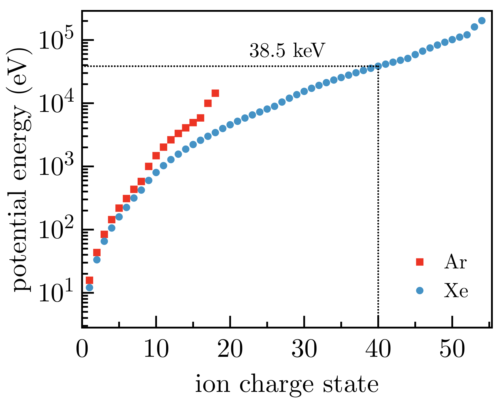
By using HCIs, we benefit from a unique property of (heavy) ions: the available potential energy resulting from the charge state. By successive removal of electrons from the atomic shells of an ion, the total ionization potential of a certain charge state is stored as the potential energy in the ion. Figure 1 shows the potential energy for Ar and Xe ions as a function of the charge state. It can reach up to several 10 keV for Xe charge states above 30. The potential energy is released as soon as the ion neutralizes and deexcites in the vicinity of a surface.
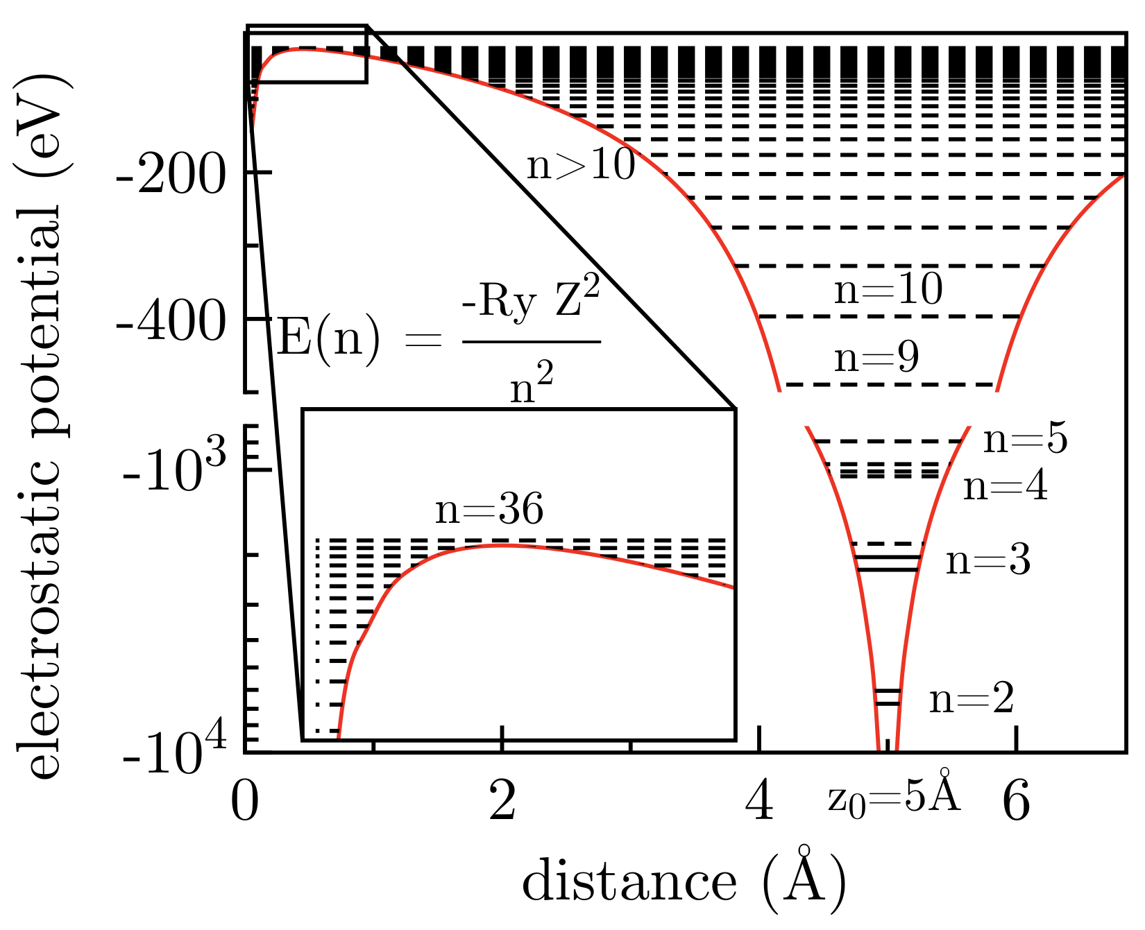
It is generally believed that, upon approach towards a solid surface, a HCI starts to capture electrons above the Coulomb barrier between the surface and the ion [6,25]. Figure 2 shows the electrostatic potential in front of a metallic surface according to the COB-model [6] for a Xe ion in close proximity of 5 Å to the atomic plane of the surface along the ion-surface axis. The potential barrier between the surface and the ion is significantly lowered allowing resonant electron transport to the ion. Electrons, which were captured resonantly, occupy states in the ion with principal quantum numbers of . Resonant charge capture is typically fast enough (<1 fs) for almost complete neutralization above the surface [26]. The neutralized atom, however, is left with a plethora of empty inner shells. It is referred to as a hollow atom [26].
Even though the COB-model works well, both as an instructive model and for quantitative comparison to grazing scattering experiments [27,28], it fails to work within a solid. As soon as the ion enters the surface (or the electron jellium), the picture of single electron transfer and isolated ionic states breaks down. However, applying a similar model description inside the solid by assuming a peel-off of the outer electrons due to their large radii and subsequent screening from surface atoms inside the binding radius was attempted [29,30]. The now recharged ion would capture electrons with significantly higher binding energies resonantly from the target atoms, stripping them from their core electrons. A hollow atom of second generation may be formed [31]. Subsequent non-radiative and radiative deexcitation in the hollow atom (or hollow ion if not entirely neutralized yet) and re-fill of emitted Auger electrons from the target leads finally to a neutral projectile in its ground state. This model for inside-the-solid neutralization appears reasonable if medium charged ions are applied and a solid of mostly heavy atoms as well as large thickness is used. Going to heavy ions with high charge states, a very light target material and single atomic thickness, we show that the model of peel-off and second generation hollow atom formation needs to be refined.
The potential energy release (see Figure 1) close to the surface may lead to significant material modification. Considering the amount of deposited energy, it may not be surprising that surface nanostructures from individual ion impacts are formed [33,34,35]. Depending on the material and the charge state, pits with desorption yields in the order of a few 1000 atoms/ion (Figure 3a), caldera-like structures (Figure 3b) and nm-sized hillocks (Figure 3c) are observed [33,35,36]. However, due to the nature of energy deposition, i.e., by electron transport and electronic deexcitation, only insulators and semi-conductors are prone to nanostructure formation by HCI impact [34,37]. The potential energy is initially converted into electronic excitations at the surface (and kinetic energy of emitted electrons). Electron–phonon coupling leads, on a longer time scale, to heating of the lattice resulting in sputtering or desorption of atoms, nano-melting or sublimation. Because the potential energy deposition is the main driving force for material removal by HCIs, it is termed potential sputtering [38]. On metals, electronic excitations get screened and dissipated before electron–phonon coupling can set in. The lattice remains cold and therefore no nanostructures are observed.
2. Experimental Results on Highly Charged Ion Transmission
The fabrication of ultrathin films, especially the production of freestanding single layer graphene, opens nowadays the possibility to study ions in the pre-equilibrium regime, and to get insights in the neutralization and deexcitation processes within the first monolayers of the solid. At projectile velocities , the equilibrium charge is typically very small (≤1) and can be estimated by Bohr’s stripping criterion [40] to be , with the nuclear charge Z of the projectile and the Bohr velocity a.u. m/s. The special combination of slow highly charged projectile ions with charge states far from equilibrium and ultrathin membranes is therefore ideally suited to study pre-equilibrium phenomena.
Although experimental investigations with truly two-dimensional (2D) materials are only possible for a few years, first attempts to study HCI interaction processes with thin materials go back more than twenty years and are shortly reviewed in the next section.
2.1. Earlier Work
In a first attempt to determine the distance an ion travels in a solid until it reaches its equilibrium charge state, Herrmann et al. [12] investigated the energy loss and final charge state distribution of slow ( ) Ar ions ( 8, 12, and 16) after transmission through a freestanding 31 nm thick carbon foil. Within the experimental resolution, they could not find a dependence on the projectile’s initial charge state and therefore concluded that the ions reach their charge state equilibrium after passing a few atomic layers only. Furthermore, transmission measurements through thinner carbon foils (10 nm and 5 nm) performed by Hattass et al. [41] could show that HCIs reach their equilibrium charge state after the transmission of a 10 nm thick foil but not after the passage of only a 5 nm thick carbon foil. Evaluating the average exit charge state in dependence on the projectile velocity (0.25–0.46 ), the charge equilibration time in the carbon foil could be estimated to be less than 7 fs. Since sequential filling of the ion’s inner-shell vacancies would probably take much longer than the evaluated equilibration time of only a few fs, the authors concluded that multiple Auger transition cascades must proceed in parallel to facilitate such a rapid equilibration [41].
Besides transmission measurements, similar results were also obtained by performing scattering measurements with HCIs. Folkerts et al. [42] investigated the final charge state distribution of multiply charged O ions with 3–8 scattered under grazing angles of incidence from a gold surface and observed almost complete charge equilibration. With projectile trajectory calculations, they could show that the projectiles spend less than 30 fs within 2 Å of the topmost Au layer. They concluded that already at the target interface strong screening effects have to be present which result in a significant upward shift of the projectile energy levels, enabling a direct capture of electrons into the L and M shell. Similar scattering processes were performed by Winecki et al. [43], who investigated the final charge state distribution of highly charged Ar ions ( = 4–17, 0.15–0.62 ) scattered under grazing angles of incidence from a smooth highly oriented pyrolytic graphite surface. It was found that independent of their initial charge state, the scattered projectiles leave the surface virtually fully equilibrated. They explained the fast neutralization process and the X-ray spectra measured in coincidence with grazingly scattered ions by side feeding processes of electrons into the L and K shell.
Apart from transmission measurements and scattering experiments, observation of fast electron ejection and measurements of the exit projectile charge state distribution after frontal collision of Xe ions with C were performed by Martin et al. [1]. This model system of a large atomic cluster with a small diameter limiting the ion’s transmission time to less than 3.2 fs is already very close to a truly 2D solid surface. The assumption of greatly enhanced Auger rates was found to be necessary to interpret the observed fast electron ejection during the collision time.
As long as neutralization is incomplete, charge state effects on the energy loss also become experimentally accessible. An enhancement of the average energy loss value as a function of the incident charge state was reported by Schenkel et al. [44]. They performed transmission measurements with Xe and Au ions ( ) in high charge states () through 10 nm thick carbon foils. In comparison to these measurements, in scattering measurements performed by Winecki et al. [45], a charge dependent energy loss could not be observed, which was, in turn, interpreted as indication for full neutralization of the projectile before reaching the distance of the closest approach.
2.2. Our Work
Recently, we made a step forward and presented transmission measurements with ultrathin membranes. We started with 1 nm thick carbon nanomembranes (CNM) and focussed then on the ultimately thin material, a freestanding single layer of graphene (SLG).
The experimental procedure follows traditional beam-foil experiments, i.e., ions are provided by an ion source (electron beam ion trap from Dreebit GmbH, Germany) and are charge-over-mass selected by either an analyzing magnet or a Wien filter. Ions are focused on a sample and are measured after transmission through the sample with an electrostatic analyzer or a time-of-flight spectrometer. For the latter, we chop the beam by a fast switching electrostatic beam blanker. The ion kinetic energy is adjusted by an electrostatic retarding field between the beamline (insulated) and the target chamber. Samples are mounted on a Transmission Electron Microscopy (TEM) grid with a supporting Carbon film (Quantifoil). The Quantifoil has regularly sized and spaced holes, which are over-span by the freestanding 2D material. The target chamber is kept at low mbar or high 10 mbar to prevent charge exchange of the ions with the rest gas as well as keeping the samples free of contaminations as good as possible. Details in the experimental setups can be found in [24,46].
2.2.1. Carbon Nanomembranes
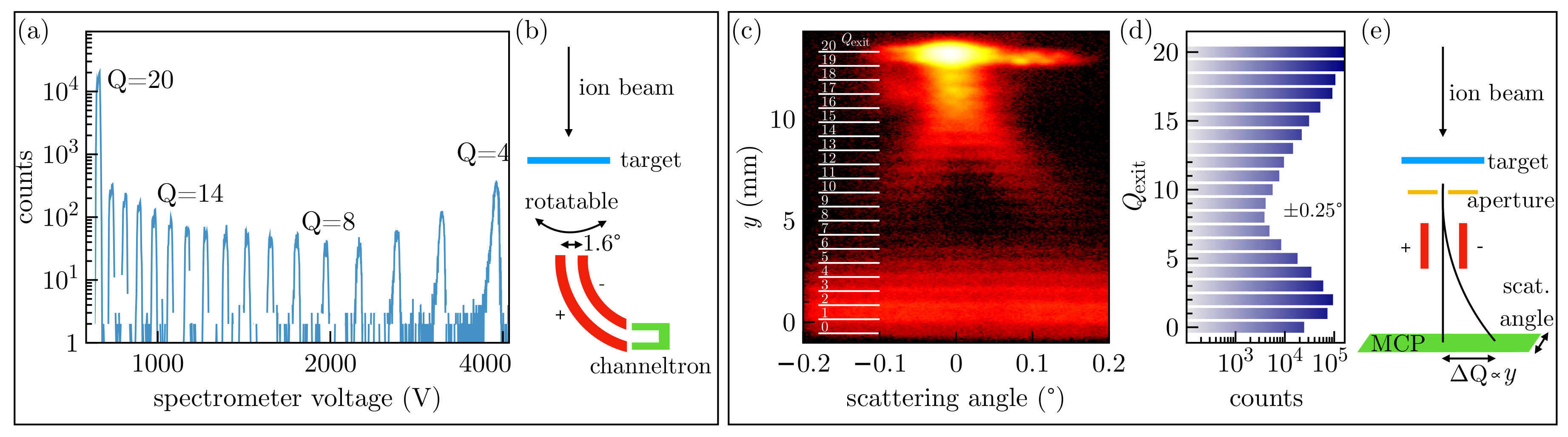
Cross-linking of a self-assembled monolayer of organic molecules by low energy electron irradiation can lead to a closed and mechanically stable membrane, which can be released from a substrate and used as a freestanding sheet [47]. Using 1,1-Biphenyl-4-thiol as a molecular precursor results finally in a 1 nm thick carbon nanomembrane [48]. The sheet thickness is small enough to enable highly charged ion transmission such that the transmitted ions have not yet reached their charge state equilibrium [19]. In this way, we are able to address pre-equilibrium charge exchange and stopping directly. Figure 4a shows a spectrum of charge states obtained with an electrostatic analyzer in forward direction and an acceptance angle of 1.6° (see Figure 4b). Xe ions with a kinetic energy of 90 keV were used. Each peak can be assigned to an exit charge state. The position of the peaks is given by the ion energy loss and the width of each peak is determined by the ion energy straggling. The large peak at results from ions, which pass uncovered areas from the sample. These areas cannot be avoided, because 2D materials cover a supporting TEM grid only partially and rip apart due to mechanical stress. However, the “primary peak” at allows an energy calibration inherent to every spectrum, because these ions did not exhibit energy loss. The spectrum in Figure 4a shows even more peaks at lower charge states with a decreasing height from to and and increasing abundance from to . With an electrostatic analyzer, we are limited to a certain maximal voltage, which, in turn, limits the maximal observable charge exchange. Further, ions transmitted as neutral atoms cannot directly be observed. The decreasing and increasing intensities of exit charge states are in fact two distinct charge state distributions, as shown by angle-resolved measurements recently [19].
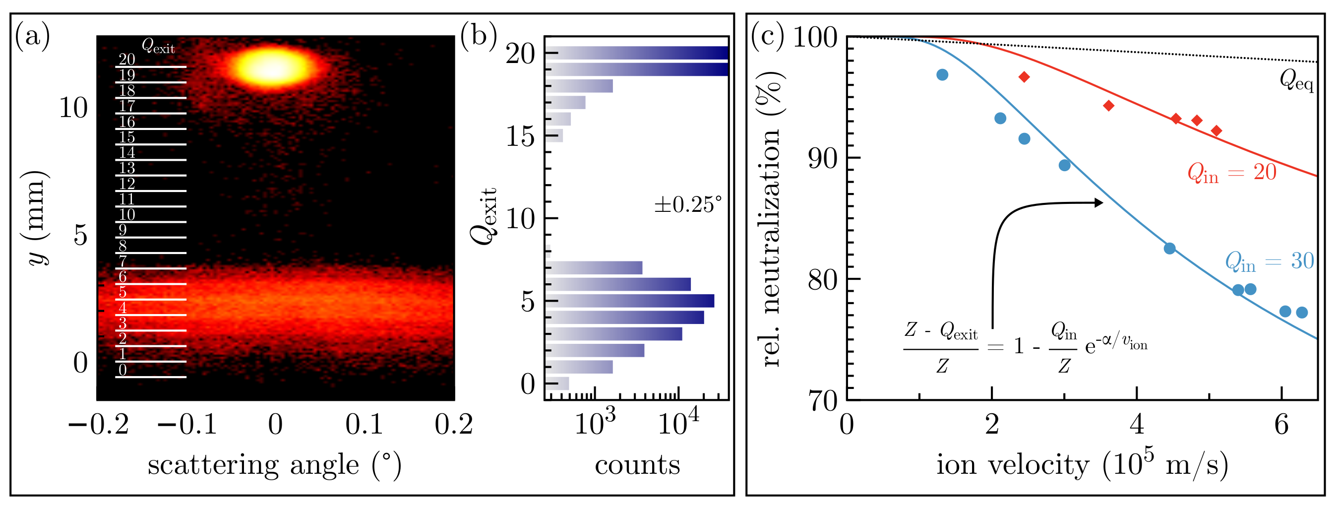
Using a different detection technique, i.e., a multi-channel plate with a delay-line detector (DLD), enables a two-dimensional position determination of transmitted ions (see Figure 4e) [24]. Limiting the scattering angle in one direction (vertical) with a slit aperture and using a set of deflection plates, we can resolve both, charge exchange and scattering angle, at the same time for all transmitted charge states (including neutral atoms) in parallel. Figure 4c shows a charge exchange spectrum from 180 keV Xe with this detection technique. The ion parameters are, and thus the spectrum is, comparable to the data shown in Figure 4a. Along the y-axis, lines appear of different intensities (color) resulting from different exit charge states. The scattering angle is shown along the x-axis. The DLD can be moved along the horizontal axis up to 10° to cover a wide range of scattering angles with subsequent measurements (not shown here). Integrating the exit charge state intensities in an angular range of results in the exit charge state spectrum shown in Figure 4d. The spectrum is similar to the data presented in Figure 4a, whereas it also includes charge states Q = 0–3. It shows that the second, low exit charge state distribution indeed peaks at . Interestingly, the angular dependence of the charge exchange can here be observed directly with a resolution of about , not possible with the electrostatic detector set-up. Low exit charge states i.e., 0–6 are scattered into a broad angular range, whereas the maximum scattering angle for Xe on C is given by momentum conservation and amounts to about 5.3°. This observation was already made earlier with angle-resolved measurements utilizing the electrostatic detector set-up and led to the conclusion, that ions in low exit charge states are scattered at small impact parameters and are subsequently deflected under larger angles [19]. Ions in the first, high exit charge state distribution are scattered within an angular range of about with a charge state dependent scattering pattern. Charge states of Q = 14–19 are transmitted directly into forward direction indicating no angular deflection (angular spread is comparable to the “primary peak” at ) or, in turn, they are scattering with large impact parameters (≳1.5 Å [19]). Now, ions at charge states Q = 7–13 are transmitted in angles of 0.05–0.15°, i.e., not in straight forward direction. From the classical scattering integral
we can calculate the impact parameter for these particular scattering angles and thus derive the impact parameter dependence of charge exchange [21]. In Equation (1), the scattering angle is given in the center-of-mass (cms) system. is the distance of closest approach of the projectile and the target atom, p the impact parameter, R the interatomic distance, the ion kinetic energy in the cms and is the scattering potential. The scattering potential is charge state dependent. Thus, for each incident charge state (and to some extent each charge exchange value), the scattering integral must be evaluated [21,49]. However, the evaluation and the comparison with the COB-model for the high exit charge states () is beyond the scope of this paper.
At this point, we see for CNMs two exit charge state distributions, one at high and one at low exit charge states. Both distributions also show distinctly different angular scattering patterns, whereas high exit charge states are observed mainly under straight forward direction () and low exit charge states at all angles within 0–5.3° (or larger angles resulting from multiple scattering).
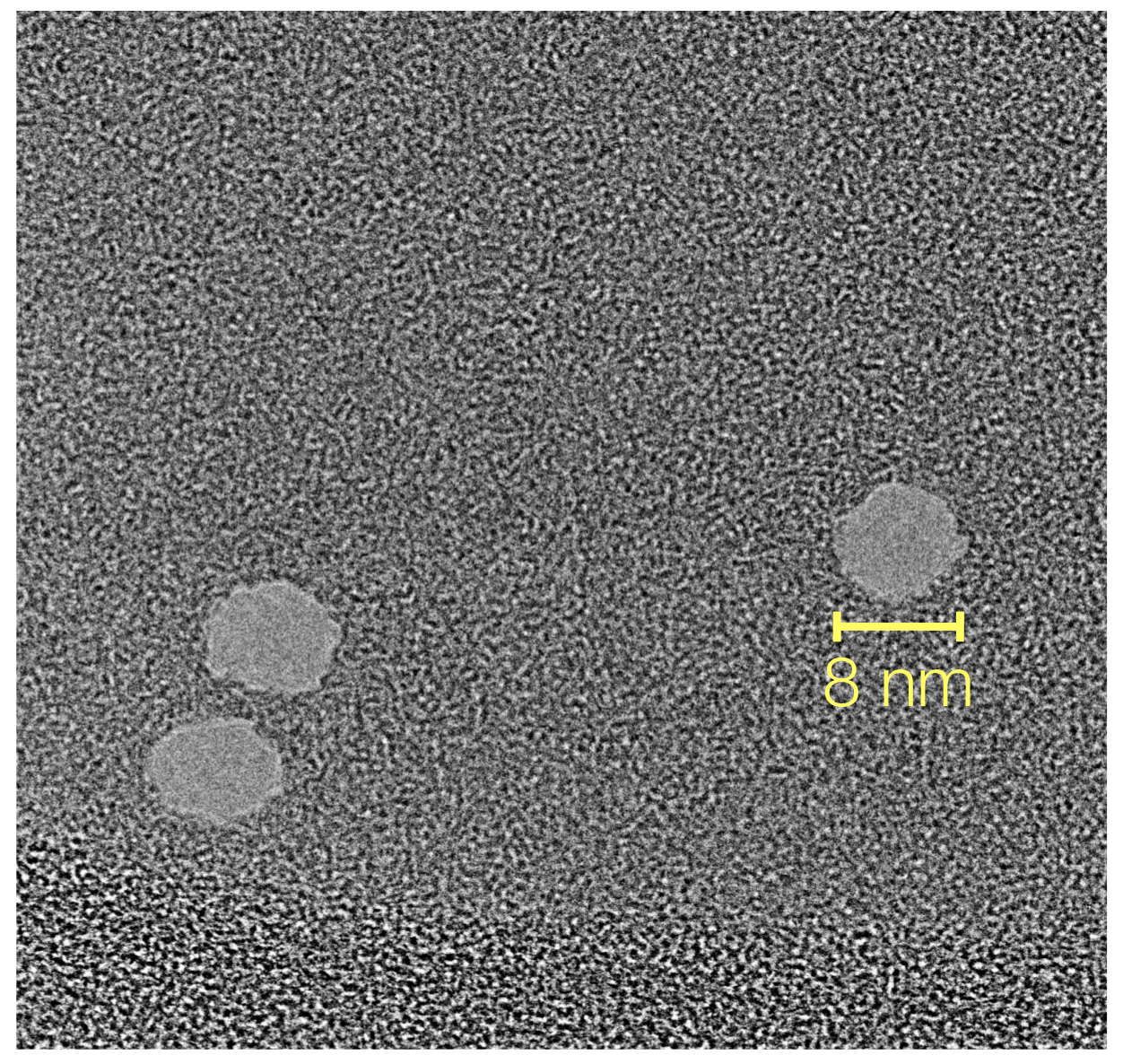
As the charge exchange in CNMs is large, i.e., HCIs are almost neutralized in 1 nm thick carbon membranes (for the low charge state distribution), a large amount of potential energy is deposited (see Figure 1). This potential energy deposition leads to the formation of large pores with diameters of several nanometers in CNMs (see Figure 5). A single HCI removes about 100–1000 atoms, which is a potential sputtering yield comparable to the case of 3D target surfaces (see Figure 3a) [18,20]. The mean size of the pores can be adjusted by the incident charge state in a range of 0 () to about 17 nm (40 keV Xe) in diameter. Even though the mechanism for pore formation is still not entirely clear, the insulating behaviour of CNMs makes them prone to HCI induced nanostructuring. Deposited positive charge and trapped electronic excitations at the impact site, as a result of the charge exchange, may not be screened fast enough before atoms from the material are set in motion. Thus, potential sputtering may occur as a result of a simple bond breaking with subsequent desorption. Another explanation is Coulomb explosion [50], although it was excluded for the 3D cases shown in Figure 3a–c [51].
2.2.2. Single Layer Graphene
Graphene is not only thinner than CNMs, it is in fact the thinnest solid state material. It also has a well defined crystallographic structure and, as a zero band gap semi-metal, a high electrical conductivity [52]. In this section, we show how HCI neutralization proceeds in a freestanding single layer of graphene (SLG). Samples are produced by standard chemical vapor deposition with a carbon containing gas (e.g., methane) on a Cu foil. The self-limiting growth on catalytic surfaces leads to the formation of a single layer of graphene [53]. By using a Cu foil, which is polycrystalline, several graphene domains are formed, differing in their rotational lattice alignment. As a result, the SLG we used has single crystalline domain sizes of a few hundred nanometers in diameter and grain boundaries between them. The grain boundaries limit the mechanical stress our SLG can withstand. The as-grown SLG is transferred from the Cu foil without the use of a spin-coated polymer film onto a Quantifoil TEM grid. The Quantifoil support structure is a 20–50 nm thick carbon material with regularly sized (d = 1.2–2 μm) and spaced holes, which are covered by our SLG. The absence of a polymer layer during transfer is essential for our HCI transmission studies. PMMA as the most commonly used polymer cannot be entirely dissolved by acetone afterwards, leaving nm-thick residuals on the graphene layer [54]. Our samples are additionally cleaned using a method described in [54]. Samples brought into the HCI irradiation chambers were heated up to 200 °C, whereas no change in measured charge exchange was observed with increasing target temperature. We cannot entirely exclude remaining contamination of our freestanding SLG samples. Ex-situ performed scanning TEM (STEM) measurements indicate clean, uncontaminated areas of about 50-70% of the sheet. Due to the lack of in-situ atomically resolved microscopy, we do not know if contaminations are always present or arise again from the sample transport in air.
Figure 6a,b shows an angle resolved charge exchange spectrum of Xe at 180 keV kinetic energy transmitted through SLG. The experimental conditions are the same as for the measurement in Figure 4c. Differences between CNM and SLG become immediately clear. First, there is only one charge state distribution visible between and 8 (note the log-scale in Figure 6b and compare to Figure 4c). Secondly, the distribution peaks at about , instead of 2 for CNM. This results from the reduced thickness of SLG and subsequently from a shorter interaction time of the HCIs with SLG. Varying the kinetic energy of our ions allows us to adjust the interaction time in the order of 1–10 fs [2]. Figure 6c shows the relative neutralization of Xe and Xe for different velocities. is here the mean of the exit charge state distribution (e.g., 5 in Figure 6b). For low velocities ( m/s) ions are almost neutralized (>90%). For higher velocities, neutralization is incomplete, but still the charge exchange is large (≈22 captured electrons for Xe at m/s). As a comparison, the equilibrium charge state is also shown in Figure 6c, indicating that our HCIs are not yet in charge equilibrium.
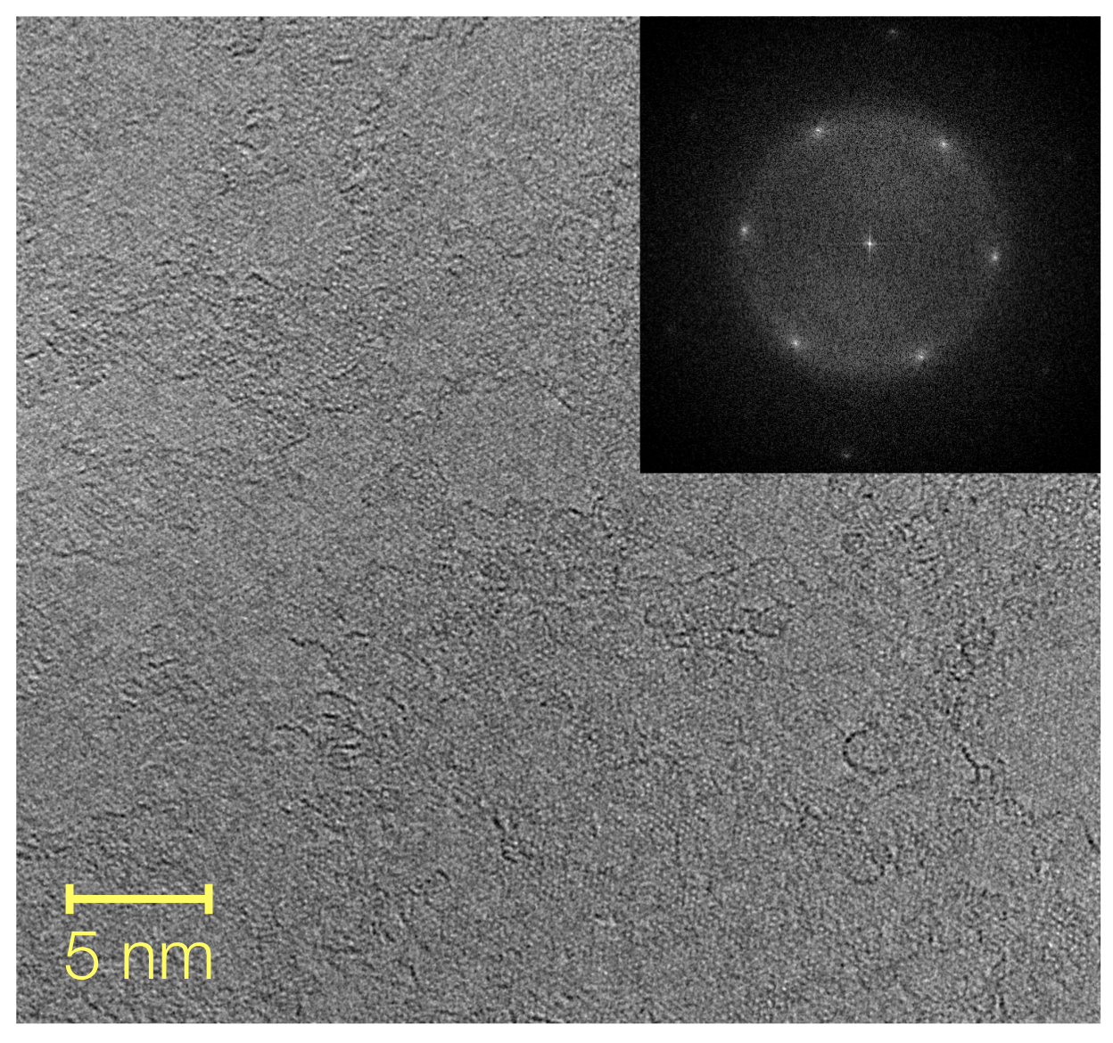
In light of the large charge exchange and potential energy release as well as the two-dimensional confinement of the ion-induced electronic excitations, visible modifications could be expected on (semi-)metallic graphene. To our surprise, SLG remains intact without observable ion-induced modifications. Figure 7 shows an atomically resolved TEM image with a field-of-view (FoV) of nm. The inset shows a fast-fourier transform of the image indicating a single crystallographic orientation of the SLG in this image. Residual contaminations are visible as varying grey contrast probably as a result of sample transport in air to the microscope. 180 keV Xe were applied and a several nm area was screened at atomic resolution. Note that ion fluencies between 100 and 10 ions/m can be applied at maximum and (S)TEM measurements at atomic resolution demand typically FoVs of nm or smaller. Hence, many microscopy images were taken from different samples to gain statistical certainty about the absence of HCI induced pores. Irradiations were performed over several hours and even days, because of low ion fluxes provided by the HCI sources. Since we do not see gradual changes in the transmission over days, we conclude that additional contaminations from the background gas in our experimental chambers have a minor effect compared to contaminations from the (wet-chemical) transfer procedure.
3. Discussion on Ion Interaction with 2D Materials
Let us start to discuss the results obtained with SLG as a simpler target model system and continue then with the interpretation of the CNM results, putting our findings finally into context with HCI irradiation of 2D materials on substrates.
3.1. Single Layer Graphene
The charge exchange of highly charged ions
depends on the interaction time t and a time constant for neutralization . We could show that the neutralization time constant is in the range of 1–5 fs, depending on the incident charge state ()) [2,23]. At the same time, the ion energy loss depends quadratically on the incident charge state as well as on the charge exchange .
With the help of time-dependent density functional theory (TD-DFT) simulations [2], adapted for highly charged ion impact, a fast above-surface charge transfer is observed similar to the predictions of the COB-model. In addition, an energy loss, which scales quadratically with the incident charge state, was observed. From the simulations, an intuitive picture of charge state dependent energy loss of slow ions (above the surface) can be drawn. As soon as the ion extracts electrons from the graphene, a positive charge patch is formed. Transported electrons need to reverse their momentum vector to follow the ion, i.e., after extraction they need to turn around. Since the ion is further approaching the surface, captured electrons lag behind the ion forming a negatively charged wake (similar to the findings for swift ions close to the surface [55]). At this point, the unscreened ion charge (screening is anisotropic due to the wake) and the transiently formed charge patch lead to a retarding Coulomb force. The ion charge at this point is proportional to the incident value. The amount of positive charge of the charge patch will also be proportional to the ion incident charge state and thus the stopping force is proportional to . After the ion passed the graphene layer, the TD-DFT simulations show an isotropic screening of the ion nuclear charge and thus no long-range Coulomb forces act on the ion after passage. Our measurements, and to some extent the simulations, show that ion stopping in the pre-equilibrium regime depends on the incident charge state as well as on the amount of charge exchange. Thus, there exists a close connection between ion stopping and the ion’s neutralization dynamics.
The simulations further predict a large in-plane current density of electrons moving towards the impact area and neutralizing the impact zone. As a result, pore formation is suppressed.
The TD-DFT simulations [2] give nice explanations for the observed stopping force and describe the electron transport before the ion impacts on the graphene layer well. However, they cannot take atomic and inter-atomic deexcitation processes into account. The lack of deexcitation processes in the TD-DFT simulations leads to a simulated charge exchange, which is independent of the ion velocity. This is in contradiction to experimental data, e.g., in Figure 6c.
Energy is transferred to the target by ion stopping (few keV, see above) as well as ion neutralization and deexcitation. The latter is the potential energy deposition (few 10 keV) and may even be greater than the energy deposition by stopping. The formation of a hollow atom in front of the material’s surface, as it is described by the COB-model, is dominated by resonant charge transfer, i.e., the potential energy remains stored in the ion as the total excitation potential of the hollow atom. It is the ion’s deexcitation which releases the potential energy. Deexcitation in hollow atoms is, to a major extent, driven by non-radiative Auger-type processes. Radiative processes contribute only to a minor extent, because of small transition rates [56,57].
To identify which Auger-type processes (atomic or intra-atomic) are dominating, we need to reconsider the measured neutralization time constants of 1–5 fs and compare those with the typical Auger deexcitation lifetimes. Atomic deexcitation, especially in the outer shells , proceed on the 1–100 fs time scale [58]. Hence, they are active mostly when the ion has passed the graphene sheet already. Consequently, the deexciting hollow atom emits (energetic) Auger electrons and charges up again. Further supply of electrons to the ion is prohibited, because it is not in contact with the target anymore. Our observed low exit charge states, and even neutral projectiles at m/s, are in conflict with this description.
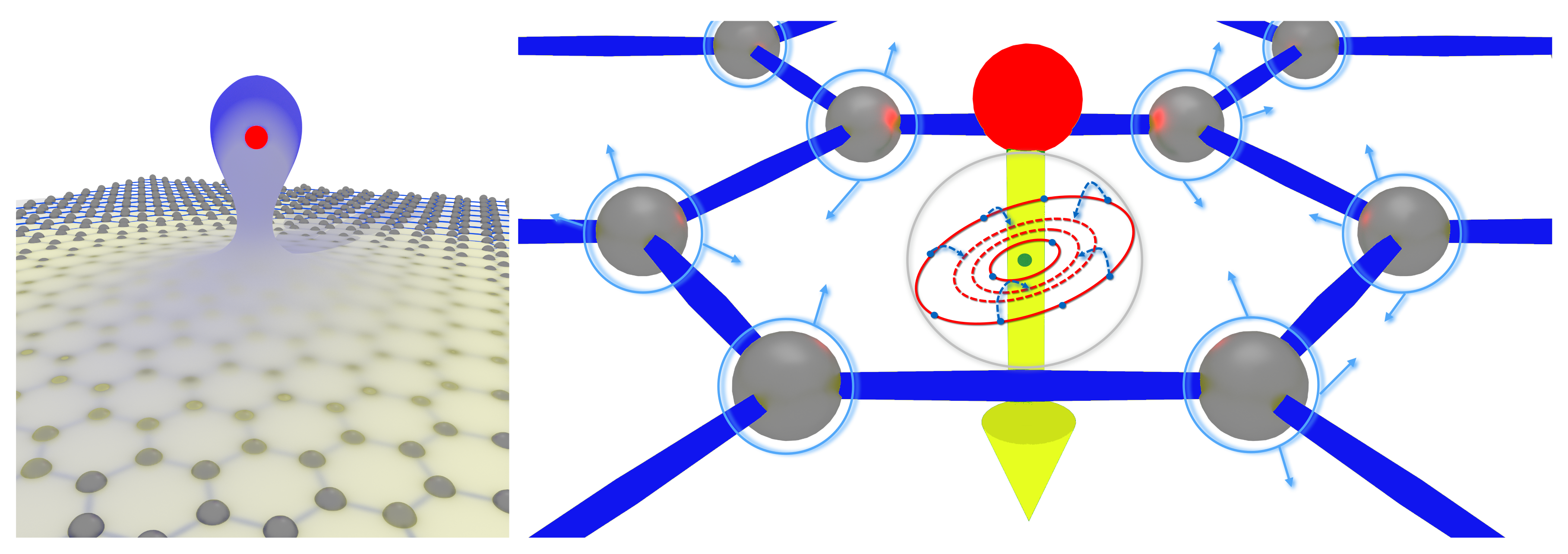
After a hollow atom has formed above the surface, a deexcitation process must be active, which suppresses electron loss by auto-ionization. It can only appear in close contact with a large atomic cluster or a solid surface by energy release to the target atoms [59]. Related processes are termed electron transfer mediated decay (ETMD) and interatomic coulombic decay (ICD) [60]. ETMD involves non-resonant target electron transfer directly into core-levels of the ion and energy uptake by another target electron. It is ineffective in our case, because of a small wave function overlap of the target electron with the core orbital of a highly charged ion (see Figure 2). ICD, however, is an energy release mechanism without electron transfer. Outer projectile electrons, in our case previously (COB) transported electrons, transfer their excitation energy to valence electrons of the target, which also have a large spatial extent. The energy transfer works via electron–electron interaction. In this way, outer electrons in a hollow atom can deexcite by excitation (and ionization) of target electrons and without ionization of projectile electrons. ICD has a lifetime or rate, which depends strongly on the interatomic distance of the projectile and the target as well as on the target size, i.e., number of nearest neighbours [61,62,63]. The closer the projectile and the target get, or the more target atoms donate electrons to the process, the stronger the electron–electron interaction and the faster ICD becomes. The lifetime of ICD is in the range of 1–5 fs, i.e., well in the range of our ion–SLG interaction time [62]. The ratio of ICD lifetime and HCI interaction time defines a competition between survival of outer projectile electrons (later auto-ionized) and hollow atom quenching (without recharging). Thus, it defines the amount of potential energy, which can be transferred to a 2D target and it explains our observed velocity (and time) dependence of charge exchange.
In summary, HCI neutralization proceeds as a two-step process [23] depicted in Figure 8. At first, the HCI extracts electrons classically over the Coulomb barrier between ion and surface. Electrons are transferred resonantly, i.e., no potential energy is transferred or released. The electrons are weakly bound to the ion in orbitals with high quantum numbers and large spatial extent (≤10 Å). The extraction of the electrons forms a positive charge patch at the surface. The reversal of the direction of motion of the transferred electrons leads to a distortion of the bound electron density. A Coulomb force acts on the ion and contributes to its stopping.
As soon as the ion is close enough to the surface atoms, ICD sets in and leads to a fast deexcitation of the projectile’s outer electrons by excitation of target electrons. The target surface is further positively charged by electron ionization (observable in experiment as a high yield of slow electrons) and atomic bonds in the impact area are weakened by excitation of target electrons from the valence band into the conduction band (binding to anti-binding states). If the ion is initially slow enough (, if a.u. is the ICD rate for interatomic distances <1 Å [62] and d the target thickness), ICD wins over and the ion is measured as a neutral particle in the detector. If the ion has a finite velocity in the range of a few m/s (>1 Å/fs, i.e., >0.04 a.u.), ICD can only partly succeed and some electrons remain in highly excited states after the ion passed the 2D target. The excited electrons will now continue to deexcite leading to auto-ionization and subsequent recharging of the ion. As a result, an ion in an intermediate charge state is measured. The statistical nature of the ICD process, i.e., which levels are populated, and the Auger-type auto-ionization lead to the width of the exit charge state distribution. Whether electrons emitted by ICD (from target atoms) and those from partly deexcited ions (at a later stage) can be distinguished by their energy (or angular distribution) needs to be clarified in future experiments.
Electronic excitations in the surface produced by ICD of hollow atoms can later drive nanostructure formation at insulating surfaces (see Figure 3a–c) and perforation of 2D insulators (see Figure 5) due to electron–phonon coupling or Coulomb explosion [64]. At metallic surfaces or metallic 2D materials, electronic excitations are highly mobile and dissipate the excitation energy on a time scale much faster than atomic motion at surfaces. Before atoms can be displaced, i.e., electron–phonon coupling can set in, the (electronic) energy density gets small.
3.2. Carbon Nanomembranes
With our knowledge on the neutralization dynamics of HCI and the interatomic distance dependence of the deexcitation mechanism, we can also explain the ion spectroscopy results obtained with CNM (see Figure 4a–e). The low exit charge state distribution is a result from small impact parameter scattering, as we know from the broad angular distribution. At these small impact parameters, ICD is active and, as a result, ions are transmitted in low charge states.
CNMs are 1 nm thick (≈3 carbon–carbon bond lengths) leading to a longer interaction time than in case of SLG. The charge state distribution peaks at lower charge states. At the same time, the (areal) density of carbon atoms in a CNM can be estimated from the coverage density of the self-assembled monolayer used to fabricate CNMs. Assuming no carbon loss during the cross-linking and formation of CNM, the areal density is at/cm. This value is only 1.4 times larger than the areal density of SLG. A three-times-larger thickness, but only 1.4-times-larger amount of atoms in a unit area, results in a two-times-lower average density of CNM compared to SLG. Since CNMs appear amorphous, the density will show local variations with dense and underdense areas, allowing a broader range of impact parameters our HCIs can have. HCIs passing through underdense areas are scattered under larger impact parameters and subsequently ICD is ineffective or even absent. Ions will capture electrons resonantly and exhibit a deexcitation cascade as an isolated atom on its way to the detector. The result is a highly charged ion again with only a few stabilized electrons, i.e., the high exit charge state distribution. HCIs ending up in this distribution experience solely COB electron capture and no further electronic interaction with the target. Scattering into 0.05– 0.15° results then only from distant elastic scattering.
3.3. 2D Materials on Substrates
In contrast to the studies of freestanding 2D materials discussed above, SLG and SL-MoS were investigated after HCI irradiation when placed on a substrate by other groups [3,65,66,67,68]. In the case of graphene on SiO and keV Xe irradiation, ion-induced defects were observed as enhanced friction in contact mode AFM [66]. No topographic changes were observed. Additionally, the Raman signal shows a clear defect related D-peak after ion irradiation. The absence of topographic nanostructures in AFM was also reported before for HOPG samples [18]. In another study, SLG was placed again on SiO and contacted by Ti/Au contacts [3]. The Si underneath the 285 nm thick SiO served as a back gate for this field-effect transistor design. Studies showed again an ion-induced D-peak in the Raman spectra as well as a reduced carrier mobility for both, electrons and holes, with increasing HCI fluence. Furthermore, 4 MeV Kr ions were used to irradiate SLG on 300 nm SiO [68]. Raman spectroscopy again showed an increase in D-peak intensity with ion fluence. For 260 keV Xe and Xe irradiation of SL- and multilayer-MoS on KBr(100) substrate, ion induced nanofeatures were observed as both holes and hillocks on monolayer and bulk MoS, respectively. All the studies on substrates were performed with significantly higher kinetic energies than the studies on freestanding 2D materials, i.e., the ions interact only for 0.3–2 fs with the SLG and MoS. Potential energy can therefore not be transferred efficiently into the SLG (ICD is not fast enough). It must be assumed that the larger part of the potential energy is deposited in the insulating substrate and leads there to modifications. A local phase transformation of the substrate underneath the SLG may then damage the SLG leading to point defects or rotational defects. These defects will not appear as topographic nanostructures in AFM, but will contribute to a D-peak in Raman spectroscopy, reduced carrier mobility, as well as to enhanced friction in contact-mode AFM. It can further not be excluded that deposited positive charge of the ion in the insulating substrate forms a stable charge patch underneath the SLG serving as scattering centers for charge carriers. In the case of SL-MoS, it was assumed that potential energy driven pits on the KBr substrate underneath are formed [65]. With even higher kinetic energies of several 10 MeV to GeV, ion-induced folding openings (grazing incident angle [69]) were observed on freestanding SLG. These studies are addressing the realm of swift heavy ions, which have some similarities to HCI in the respect of initial energy deposition to the electronic subsystem [70,71]. However, ICD may not be active for swift heavy ions, i.e., the energy transfer process is different yielding also different nanostructuring efficiencies.
4. Conclusions
With ion transmission spectroscopy, we are able to measure the charge exchange and energy loss of highly charged ions in insulating CNM and (semi-)metallic SLG. Both materials show a very fast neutralization and deexcitation process leading to the capture and stabilization of several 10 s of electrons during the interaction time of <10 fs. The insulating and conducting character of CNM and SLG, respectively, seem to be unimportant for the ion neutralization dynamics. For CNM, with their inhomogeneous density, a second, distinct charge state distribution is observed as a result of pure resonant over-barrier electron transport and subsequent Auger-type deexcitation leading to recharging. On a much longer time scale, i.e., when the ion is long gone, induced electronic excitations and charges at the target surface may lead to material disintegration (nanopores) on insulating surfaces and membranes. For highly conducting surfaces, nanostructuring was not observed, supported by the fact that excited charge carriers are quickly dissipating the excitation energy in a metal.
Author Contributions
E.G., R.A.W. and J.S. conceived, designed and performed the experiments; E.G., R.A.W., J.S. and R.H. analyzed the data; S.F. and F.A. contributed to the interpretation and discussion; R.A.W. and E.G. wrote the paper; and all authors commented on the paper.
Acknowledgments
We acknowledge funding by Austrian Science Fund (FWF) (project number: I1114-N20), the German DFG (project number: WI 4691/1-1), and the TU-D doctoral college of TU Wien. We would like to thank our collaborators for the continuous support during the past 10 years, in particular A.S. El-Said for his stimulating work on ionic crystal surfaces, M. Schleberger for her support with the graphene samples and fruitful discussions, A. Gölzhäuser and A. Turchanin for their support with the CNM samples, R. Hübner and B.C. Bayer-Skoff for their support with TEM measurements, A. Arnau and A.G. Borisov for their strong support with TD-DFT calculations and fruitful discussions, J.R. Crespo López-Urrutia for making us aware of the importance of interatomic Auger processes, H. Winter for making the time-of-flight spectrometer available to us, and C. Lemell, F. Libisch, and J. Burgdörfer for many discussions improving our understanding of the underlying processes.
Conflicts of Interest
The authors declare no conflict of interest. The funding sponsors had no role in the design of the study; in the collection, analyses, or interpretation of data; in the writing of the manuscript, and in the decision to publish the results.
References
- Martin, S.; Brédy, R.; Bernard, J.; Désesquelles, J.; Chen, L. Very Fast Hollow-Atom Decay Processes in Xe30+ − C60 Collisions. Phys. Rev. Lett. 2002, 89, 183401. [Google Scholar] [CrossRef] [PubMed]
- Gruber, E.; Wilhelm, R.A.; Pétuya, R.; Smejkal, V.; Kozubek, R.; Hierzenberger, A.; Bayer, B.C.; Aldazabal, I.; Kazansky, A.K.; Libisch, F.; et al. Ultrafast electronic response of graphene to a strong and localized electric field. Nat. Commun. 2016, 7, 13948. [Google Scholar] [CrossRef] [PubMed] [Green Version]
- Ernst, P.; Kozubek, R.; Madauß, L.; Sonntag, J.; Lorke, A.; Schleberger, M. Irradiation of graphene field effect transistors with highly charged ions. Nucl. Instrum. Methods Phys. Res. Sect. B Beam Interact. Mater. Atoms. 2016, 382, 71–75. [Google Scholar] [CrossRef]
- Djebli, M.; Kiouche, A.; El-Said, A.S.; Bahlouli, H. On the formation of surface nanostructures induced by slow highly charged ions. Phys. Plasmas 2017, 24, 072115. [Google Scholar] [CrossRef]
- Peng, H.; Sun, M.; Liu, F.; Yang, D.; Zhang, D.; Yuan, W.; Du, X.; Chen, H.; Wang, L.; Wang, T. Potential effect on the interaction of highly charged ion with graphene. Nucl. Instrum. Methods Phys. Res. Sect. B Beam Interact. Mater. Atoms 2017, 407, 291–296. [Google Scholar] [CrossRef]
- Burgdörfer, J.; Lerner, P.; Meyer, F.W. Above-surface neutralization of highly charged ions: The classical over-the-barrier model. Phys. Rev. A 1991, 44, 5674–5685. [Google Scholar] [CrossRef] [PubMed]
- Arnau, A.; Aumayr, F.; Echenique, P.; Grether, M.; Heiland, W.; Limburg, J.; Morgenstern, R.; Roncin, P.; Schippers, S.; Schuch, R.; et al. Interaction of slow multicharged ions with solid surfaces. Surf. Sci. Rep. 1997, 27, 113–239. [Google Scholar] [CrossRef]
- Ducrée, J.J.; Casali, F.; Thumm, U. Extended classical over-barrier model for collisions of highly charged ions with conducting and insulating surfaces. Phys. Rev. A 1998, 57, 338–350. [Google Scholar] [CrossRef] [Green Version]
- Lake, R.E.; Pomeroy, J.M.; Grube, H.; Sosolik, C.E. Charge State Dependent Energy Deposition by Ion Impact. Phys. Rev. Lett. 2011, 107, 063202. [Google Scholar] [CrossRef] [PubMed]
- Lake, R.E.; Sosolik, C.E.; Pomeroy, J.M. Classical over-the-barrier model for neutralization of highly charged ions above thin dielectric films. Phys. Rev. A 2013, 87, 062901. [Google Scholar] [CrossRef]
- Betz, H.D. Charge States and Charge-Changing Cross Sections of Fast Heavy Ions Penetrating through Gaseous and Solid Media. Rev. Mod. Phys. 1972, 44, 465–539. [Google Scholar] [CrossRef]
- Herrmann, R.; Cocke, C.L.; Ullrich, J.; Hagmann, S.; Stoeckli, M.; Schmidt-Boecking, H. Charge-state equilibration length of a highly charged ion inside a carbon solid. Phys. Rev. A 1994, 50, 1435–1444. [Google Scholar] [CrossRef] [PubMed]
- Imai, M.; Sataka, M.; Kawatsura, K.; Takahiro, K.; Komaki, K.; Shibata, H.; Sugai, H.; Nishio, K. Equilibrium and non-equilibrium charge-state distributions of 2 MeV/u sulfur ions passing through carbon foils. Nucl. Instrum. Methods Phys. Res. Sect. B Beam Interact. Mater. Atoms 2015, 354, 172–176. [Google Scholar] [CrossRef]
- Lamour, E.; Fainstein, P.D.; Galassi, M.; Prigent, C.; Ramirez, C.A.; Rivarola, R.D.; Rozet, J.P.; Trassinelli, M.; Vernhet, D. Improvement of the ETACHA Code towards low velocities and many-electron ions. J. Phys. Conf. Ser. 2015, 635, 032022. [Google Scholar] [CrossRef] [Green Version]
- Farimani, A.B.; Min, K.; Aluru, N.R. DNA Base Detection Using a Single-Layer MoS 2. ACS Nano 2014, 8, 7914–7922. [Google Scholar] [CrossRef] [PubMed]
- Roy-Mayhew, J.D.; Bozym, D.J.; Punckt, C.; Aksay, I.A. Functionalized Graphene as a Catalytic Counter Electrode in Dye-Sensitized Solar Cells. ACS Nano 2010, 4, 6203–6211. [Google Scholar] [CrossRef] [PubMed] [Green Version]
- Kepaptsoglou, D.; Hardcastle, T.P.; Seabourne, C.R.; Bangert, U.; Zan, R.; Amani, J.A.; Hofsäss, H.; Nicholls, R.J.; Brydson, R.M.D.; Scott, A.J.; et al. Electronic Structure Modification of Ion Implanted Graphene: The Spectroscopic Signatures of p- and n-Type Doping. ACS Nano 2015, 9, 11398–11407. [Google Scholar] [CrossRef] [PubMed] [Green Version]
- Ritter, R.; Wilhelm, R.A.; Stöger-Pollach, M.; Heller, R.; Mücklich, A.; Werner, U.; Vieker, H.; Beyer, A.; Facsko, S.; Gölzhäuser, A.; Aumayr, F. Fabrication of nanopores in 1 nm thick carbon nanomembranes with slow highly charged ions. Appl. Phys. Lett. 2013, 102, 063112. [Google Scholar] [CrossRef]
- Wilhelm, R.A.; Gruber, E.; Ritter, R.; Heller, R.; Facsko, S.; Aumayr, F. Charge Exchange and Energy Loss of Slow Highly Charged Ions in 1 nm Thick Carbon Nanomembranes. Phys. Rev. Lett. 2014, 112, 153201. [Google Scholar] [CrossRef] [PubMed]
- Wilhelm, R.A.; Gruber, E.; Ritter, R.; Heller, R.; Beyer, A.; Turchanin, A.; Klingner, N.; Hübner, R.; Stöger-Pollach, M.; Vieker, H.; et al. Threshold and efficiency for perforation of 1 nm thick carbon nanomembranes with slow highly charged ions. 2D Mater. 2015, 2, 035009. [Google Scholar] [CrossRef]
- Wilhelm, R.A.; Möller, W. Charge-state-dependent energy loss of slow ions. II. Statistical atom model. Phys. Rev. A 2016, 93, 052709. [Google Scholar] [CrossRef]
- Wilhelm, R.; Gruber, E.; Smejkal, V.; Facsko, S.; Aumayr, F. Charge-state-dependent energy loss of slow ions. I. Experimental results on the transmission of highly charged ions. Phys. Rev. A 2016, 93, 052708. [Google Scholar] [CrossRef]
- Wilhelm, R.A.; Gruber, E.; Schwestka, J.; Kozubek, R.; Madeira, T.I.; Marques, J.P.; Kobus, J.; Krasheninnikov, A.V.; Schleberger, M.; Aumayr, F. Interatomic Coulombic Decay: The Mechanism for Rapid Deexcitation of Hollow Atoms. Phys. Rev. Lett. 2017, 119, 103401. [Google Scholar] [CrossRef] [PubMed]
- Schwestka, J.; Melinc, D.; Heller, R.; Niggas, A.; Leonhartsberger, L.; Winter, H.; Facsko, S.; Aumayr, F.; Wilhelm, R. A versatile ion beam spectrometer for studies of ion interaction with 2D materials. Rev. Sci. Instrum. 2018. under review. [Google Scholar]
- Niehaus, A. A classical model for multiple-electron capture in slow collisions of highly charged ions with atoms. J. Phys. B At. Mol. Phys. 1986, 19, 2925–2937. [Google Scholar] [CrossRef]
- Briand, J.P.; Giardino, G.; Borsoni, G.; Froment, M.; Eddrief, M.; Sébenne, C.; Bardin, S.; Schneider, D.; Jin, J.; Khemliche, H.; et al. Decay of hollow atoms above and below a surface. Phys. Rev. A 1996, 54, 4136–4139. [Google Scholar] [CrossRef] [PubMed]
- Lemell, C.; Stöckl, J.; Burgdörfer, J.; Betz, G.; Winter, H.; Aumayr, F. Multicharged Ion Impact on Clean Au(111): Suppression of Kinetic Electron Emission in Glancing Angle Scattering. Phys. Rev. Lett. 1998, 81, 1965–1968. [Google Scholar] [CrossRef]
- Winter, H. Collisions of atoms and ions with surfaces under grazing incidence. Phys. Rep. 2002, 367, 387–582. [Google Scholar] [CrossRef]
- Stolterfoht, N.; Arnau, A.; Grether, M.; Köhrbrück, R.; Spieler, A.; Page, R.; Saal, A.; Thomaschewski, J.; Bleck-Neuhaus, J. Multiple-cascade model for the filling of hollow Ne atoms moving below an Al surface. Phys. Rev. A 1995, 52, 445–456. [Google Scholar] [CrossRef] [PubMed]
- Ducrée, J.; Andrä, H.J.; Thumm, U. Neutralization of hyperthermal multiply charged ions at surfaces: Comparison between the extended dynamical overbarrier model and experiment. Phys. Rev. A 1999, 60, 3029–3043. [Google Scholar] [CrossRef]
- Winter, H.; Aumayr, F. Hollow atoms. J. Phys. B At. Mol. Opt. Phys. 1999, 32, R39–R65. [Google Scholar] [CrossRef]
- Zschornack, G.; Musiol, G.; Wagner, W. Dirac Fock Slater X-ray Energy Shifts and Electron Binding Energy Changes for All Ion Ground States in Elements Up to Uranium, zfk–574 ed.; Inst. für Kernforschung: Dresden, Germany, 1986; p. 257. [Google Scholar]
- Heller, R.; Facsko, S.; Wilhelm, R.A.; Möller, W. Defect Mediated Desorption of the KBr(001) Surface Induced by Single Highly Charged Ion Impact. Phys. Rev. Lett. 2008, 101, 096102. [Google Scholar] [CrossRef] [PubMed]
- Tona, M.; Watanabe, H.; Takahashi, S.; Fujita, Y.; Abe, T.; Jian, S.; Nakamura, N.; Yoshiyasu, N.; Yamada, C.; Sakurai, M.; et al. Observation of HCI-induced nanostructures with a scanning probe microscope. J. Phys. Conf. Ser. 2007, 58, 331–334. [Google Scholar] [CrossRef] [Green Version]
- El-Said, A.S.; Heller, R.; Meissl, W.; Ritter, R.; Facsko, S.; Lemell, C.; Solleder, B.; Gebeshuber, I.C.; Betz, G.; Toulemonde, M.; et al. Creation of Nanohillocks on CaF2 Surfaces by Single Slow Highly Charged Ions. Phys. Rev. Lett. 2008, 100, 237601. [Google Scholar] [CrossRef] [PubMed]
- El-Said, A.S.; Wilhelm, R.A.; Heller, R.; Sorokin, M.; Facsko, S.; Aumayr, F. Tuning the Fabrication of Nanostructures by Low-Energy Highly Charged Ions. Phys. Rev. Lett. 2016, 117, 126101. [Google Scholar] [CrossRef] [PubMed]
- Aumayr, F.; Varga, P.; Winter, H. Potential sputtering: Desorption from insulator surfaces by impact of slow multicharged ions. Int. J. Mass Spectrom. 1999, 192, 415–424. [Google Scholar] [CrossRef]
- Aumayr, F.; Winter, H. Potential sputtering. Philos. Trans. R. Soc. A Math. Phys. Eng. Sci. 2004, 362, 77–102. [Google Scholar] [CrossRef] [PubMed]
- Wilhelm, R.A.; Heller, R.; Facsko, S. Slow highly charged ion induced nanopit formation on the KCl(001) surface. EPL (Europhys. Lett.) 2016, 115, 43001. [Google Scholar] [CrossRef]
- Bohr, N. The penetration of atomic particles through matter. Math. Fys. Medd. Dan. Vid. Selsk. 1948, 18, 1–144. [Google Scholar]
- Hattass, M.; Schenkel, T.; Hamza, A.V.; Barnes, A.V.; Newman, M.W.; McDonald, J.W.; Niedermayr, T.R.; Machicoane, G.A.; Schneider, D.H. Charge Equilibration Time of Slow, Highly Charged Ions in Solids. Phys. Rev. Lett. 1999, 82, 4795–4798. [Google Scholar] [CrossRef]
- Folkerts, L.; Schippers, S.; Zehner, D.M.; Meyer, F.W. Time Scales for Charge Equilibration of Oq+ (3 < q < 8) Ions during Surface-Channeling Interactions with Au(110). Phys. Rev. Lett. 1995, 74, 2204–2207. [Google Scholar] [PubMed]
- Winecki, S.; Cocke, C.L.; Fry, D.; Stöckli, M.P. Neutralization and equilibration of highly charged argon ions at grazing incidence on a graphite surface. Phys. Rev. A 1996, 53, 4228–4237. [Google Scholar] [CrossRef] [PubMed]
- Schenkel, T.; Briere, M.A.; Schmidt-Böcking, H.; Bethge, K.; Schneider, D.H. Electronic Sputtering of Thin Conductors by Neutralization of Slow Highly Charged Ions. Phys. Rev. Lett. 1997, 78, 2481–2484. [Google Scholar] [CrossRef]
- Winecki, S.; Stöckli, M.P.; Cocke, C.L. Energy loss of highly charged argon ions at grazing incidence on a graphite surface. Phys. Rev. A 1997, 55, 4310–4317. [Google Scholar] [CrossRef]
- Smejkal, V.; Gruber, E.; Wilhelm, R.; Brandl, L.; Heller, R.; Facsko, S.; Aumayr, F. A setup for transmission measurements of low energy multiply charged ions through free-standing few atomic layer films. Nucl. Instrum. Methods Phys. Res. Sect. B Beam Interact. Mater. Atoms 2016, 382, 119–122. [Google Scholar] [CrossRef]
- Turchanin, A.; Käfer, D.; El-Desawy, M.; Wöll, C.; Witte, G.; Gölzhäuser, A. Molecular Mechanisms of Electron-Induced Cross-Linking in Aromatic SAMs. Langmuir 2009, 25, 7342–7352. [Google Scholar] [CrossRef] [PubMed]
- Turchanin, A.; Beyer, A.; Nottbohm, C.T.; Zhang, X.; Stosch, R.; Sologubenko, A.; Mayer, J.; Hinze, P.; Weimann, T.; Gölzhäuser, A. One Nanometer Thin Carbon Nanosheets with Tunable Conductivity and Stiffness. Adv. Mater. 2009, 21, 1233–1237. [Google Scholar] [CrossRef]
- Biersack, J. The effect of high charge states on the stopping and ranges of ions in solids. Nucl. Instrum. Methods Phys. Res. Sect. B Beam Interact. Mater. Atoms 1993, 80–81, 12–15. [Google Scholar] [CrossRef]
- Insepov, Z.; Hassanein, A.; Swenson, D.; Terasawa, M. Computer simulation of surface modification with ion beams. Nucl. Instrum. Methods Phys. Res. Sect. B Beam Interact. Mater. Atoms 2005, 241, 496–500. [Google Scholar] [CrossRef] [Green Version]
- Neidhart, T.; Pichler, F.; Aumayr, F.; Winter, H.; Schmid, M.; Varga, P. Potential Sputtering of Lithium Fluoride by Slow Multicharged Ions. Phys. Rev. Lett. 1995, 74, 5280–5283. [Google Scholar] [CrossRef] [PubMed]
- Geim, A.K.; Novoselov, K.S. The rise of graphene. Nat. Mater. 2007, 6, 183–191. [Google Scholar] [CrossRef] [PubMed]
- Zhao, P.; Kumamoto, A.; Kim, S.; Chen, X.; Hou, B.; Chiashi, S.; Einarsson, E.; Ikuhara, Y.; Maruyama, S. Self-Limiting Chemical Vapor Deposition Growth of Monolayer Graphene from Ethanol. J. Phys. Chem. C 2013, 117, 10755–10763. [Google Scholar] [CrossRef]
- Algara-Siller, G.; Lehtinen, O.; Turchanin, A.; Kaiser, U. Dry-cleaning of graphene. Appl. Phys. Lett. 2014, 104, 153115. [Google Scholar] [CrossRef]
- García de Abajo, F.J.; Echenique, P.M. Wake potential in the vicinity of a surface. Phys. Rev. B 1992, 46, 2663–2675. [Google Scholar] [CrossRef]
- Mirakhmedov, M. Auger and X-ray spectra formed at highly charged ion neutralization near the metal surface. Nucl. Instrum. Methods Phys. Res. Sect. B Beam Interact. Mater. Atoms 1995, 98, 429–435. [Google Scholar] [CrossRef]
- Díez Muiño, R.; Salin, A.; Stolterfoht, N.; Arnau, A.; Echenique, P.M. Auger and radiative filling rates of highly charged ions below metal surfaces. Phys. Rev. A 1998, 57, 1126–1135. [Google Scholar] [CrossRef]
- Palmeri, P.; Quinet, P.; Zitane, N.; Vaeck, N. Calculation of Auger rates for complex hollow-atom configurations. J. Phys. B At. Mol. Opt. Phys. 2001, 34, 4125–4139. [Google Scholar] [CrossRef]
- Cederbaum, L.S.; Zobeley, J.; Tarantelli, F. Giant Intermolecular Decay and Fragmentation of Clusters. Phys. Rev. Lett. 1997, 79, 4778–4781. [Google Scholar] [CrossRef]
- Jahnke, T. Interatomic and intermolecular Coulombic decay: The coming of age story. J. Phys. B At. Mol. Opt. Phys. 2015, 48, 082001. [Google Scholar] [CrossRef]
- Öhrwall, G.; Tchaplyguine, M.; Lundwall, M.; Feifel, R.; Bergersen, H.; Rander, T.; Lindblad, A.; Schulz, J.; Peredkov, S.; Barth, S.; et al. Femtosecond Interatomic Coulombic Decay in Free Neon Clusters: Large Lifetime Differences between Surface and Bulk. Phys. Rev. Lett. 2004, 93, 173401. [Google Scholar] [CrossRef] [PubMed]
- Averbukh, V.; Cederbaum, L.S. Ab initio calculation of interatomic decay rates by a combination of the Fano ansatz, Green’s-function methods, and the Stieltjes imaging technique. J. Chem. Phys. 2005, 123, 204107. [Google Scholar] [CrossRef] [PubMed]
- Averbukh, V.; Cederbaum, L.S. Interatomic Electronic Decay in Endohedral Fullerenes. Phys. Rev. Lett. 2006, 96, 053401. [Google Scholar] [CrossRef] [PubMed]
- Insepov, Z.; Ainabayev, A.; Kirkpatrick, S.; Walsh, M.; Vyatkin, A.F. Nanometer size hole fabrication in 2d ultrathin films with cluster ion beams. AIP Adv. 2017, 7, 075014. [Google Scholar] [CrossRef] [Green Version]
- Hopster, J.; Kozubek, R.; Krämer, J.; Sokolovsky, V.; Schleberger, M. Ultra-thin MoS2 irradiated with highly charged ions. Nucl. Instrum. Methods Phys. Res. Sect. B Beam Interact. Mater. Atoms 2013, 317, 165–169. [Google Scholar] [CrossRef]
- Hopster, J.; Kozubek, R.; Ban-d’Etat, B.; Guillous, S.; Lebius, H.; Schleberger, M. Damage in graphene due to electronic excitation induced by highly charged ions. 2D Mater. 2014, 1, 011011. [Google Scholar] [CrossRef] [Green Version]
- Peng, H.; Sun, M.; Zhang, D.; Yang, D.; Chen, H.; Cheng, R.; Zhang, J.; Wang, Y.; Yuan, W.; Wang, T.; et al. Raman spectroscopy of graphene irradiated with highly charged ions. Surf. Coat. Technol. 2016, 306, 171–175. [Google Scholar] [CrossRef]
- Zeng, J.; Liu, J.; Yao, H.; Zhai, P.; Zhang, S.; Guo, H.; Hu, P.; Duan, J.; Mo, D.; Hou, M.; et al. Comparative study of irradiation effects in graphite and graphene induced by swift heavy ions and highly charged ions. Carbon N. Y. 2016, 100, 16–26. [Google Scholar] [CrossRef]
- Ochedowski, O.; Lehtinen, O.; Kaiser, U.; Turchanin, A.; Ban-d’Etat, B.; Lebius, H.; Karlušić, M.; Jakšić, M.; Schleberger, M. Nanostructuring graphene by dense electronic excitation. Nanotechnology 2015, 26, 465302. [Google Scholar] [CrossRef] [PubMed] [Green Version]
- Aumayr, F.; Facsko, S.; El-Said, A.; Trautmann, C.; Schleberger, M. Single ion induced surface nanostructures: A comparison between slow highly charged and swift heavy ions. J. Phys. Condens. Matter 2011, 23, 393001. [Google Scholar] [CrossRef] [PubMed]
- Wang, Y.Y.; Grygiel, C.; Dufour, C.; Sun, J.R.; Wang, Z.G.; Zhao, Y.T.; Xiao, G.Q.; Cheng, R.; Zhou, X.M.; Ren, J.R.; et al. Energy deposition by heavy ions: Additivity of kinetic and potential energy contributions in hillock formation on CaF2. Sci. Rep. 2015, 4, 5742. [Google Scholar] [CrossRef] [PubMed]
Figure 1.
(Color online) Potential energy for Ar and Xe ions as a function of the charge state, e.g., Xe has a potential energy of 38.5 keV.
Figure 1.
(Color online) Potential energy for Ar and Xe ions as a function of the charge state, e.g., Xe has a potential energy of 38.5 keV.

Figure 2.
(Color online) Electrostatic potential of a Xe ion along the ion-surface connection line normal to the surface. Binding energies for occupied levels (straight lines) are given from Hartree–Fock calculations [32] and empty states (broken lines) from Rydberg scaling of levels for heavy atoms. Level shifts due to image charge are here neglected for clarity.

Figure 3.
(Color online) (a) Atomic force microscopy image of a KCl(001) surface irradiated with 70 keV Xe ions. One- to two-monolayer-deep pits resulting from single ion impacts can be observed [33,39]. (b) AFM image of a LiF(001) surface irradiated with 99 keV Xe ions. Crater-like structures are observable [36]. (c) AFM image of a CaF(111) surface irradiated with 16.5 keV Xe ions. Hillock structures can be observed [35].
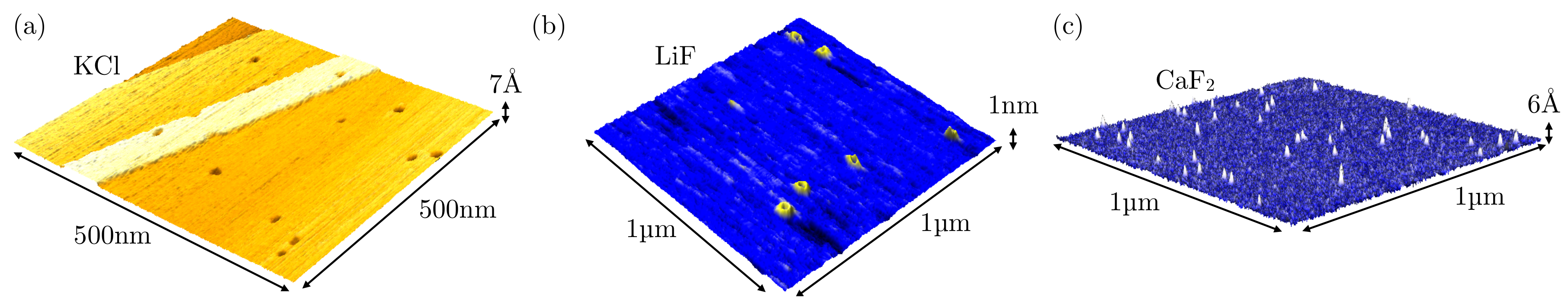
Figure 4.
(Color online) (a) Charge state spectrum of 90 keV Xe ions transmitted through a 1 nm thick freestanding carbon nanomembrane. (b) Experimental scheme for (a) with an electrostatic analyzer as a detector with 1.6° acceptance angle. (c) 2D charge state spectrum of 180 keV Xe after transmission through a 1 nm thick carbon nanomembrane with different exit charge state positions marked by white lines and the scattering angle on the abscissa (please note the log-scale). The vertical position (y) can be converted into a charge state according to the deflection by an electric field indicated in (e). (d) Integrated charge state spectrum of (c) for scattering angles between −0.25° and +0.25°. (e) Experimental scheme for (c) with a position sensitive MCP as a detector with 0.01° angular resolution.

Figure 5.
(Color online) TEM image of a CNM after 176 keV Xe irradiation. Individual nanopores can be observed as a result of single ion impacts [20].
Figure 5.
(Color online) TEM image of a CNM after 176 keV Xe irradiation. Individual nanopores can be observed as a result of single ion impacts [20].

Figure 6.
(Color online) (a) 2D charge state spectrum of 180 keV Xe after transmission through a freestanding single layer of graphene with different charge state positions marked by white lines and the scattering angle on the abscissa. (b) Integrated charge state spectrum (a) for scattering angles between −0.25° and +0.25° (please note the log-scale). (c) Relative neutralization deduced from the mean of the exit charge state distributions (e.g., see (b)) as function of ion velocity. The equilibrium charge state is given according to Bohr [40].

Figure 7.
(Color online) TEM image of SLG after 180 keV Xe irradiation. Some residual contamination can be observed on an otherwise intact graphene sheet. No single ion-induced defects can be observed. The inset shows a FFT of the image.
Figure 7.
(Color online) TEM image of SLG after 180 keV Xe irradiation. Some residual contamination can be observed on an otherwise intact graphene sheet. No single ion-induced defects can be observed. The inset shows a FFT of the image.

Figure 8.
(Color online) (left) The approaching HCI extracts electrons from the target surface while it is still at large distances. Electrons are captured in highly excited states as a result of resonant charge transfer. A hollow atom is formed. (right) At close collisions with target atoms, ICD leads to rapid quenching of the hollow atom and the emission of a large amount of low energy electrons from the target [23].

© 2018 by the authors. Licensee MDPI, Basel, Switzerland. This article is an open access article distributed under the terms and conditions of the Creative Commons Attribution (CC BY) license (http://creativecommons.org/licenses/by/4.0/).
Share and Cite
MDPI and ACS Style
Wilhelm, R.A.; Gruber, E.; Schwestka, J.; Heller, R.; Fascko, S.; Aumayr, F. Neutralization Dynamics of Slow Highly Charged Ions in 2D Materials. Appl. Sci. 2018, 8, 1050. https://doi.org/10.3390/app8071050
AMA Style
Wilhelm RA, Gruber E, Schwestka J, Heller R, Fascko S, Aumayr F. Neutralization Dynamics of Slow Highly Charged Ions in 2D Materials. Applied Sciences. 2018; 8(7):1050. https://doi.org/10.3390/app8071050
Chicago/Turabian StyleWilhelm, Richard A., Elisabeth Gruber, Janine Schwestka, René Heller, Stefan Fascko, and Friedrich Aumayr. 2018. "Neutralization Dynamics of Slow Highly Charged Ions in 2D Materials" Applied Sciences 8, no. 7: 1050. https://doi.org/10.3390/app8071050
Note that from the first issue of 2016, this journal uses article numbers instead of page numbers. See further details here.