1. Introduction
It has been well known that non-volatile memory (NVM) plays an important role in various systems with the embedded or external structures. For smart data and smart sensor applications, data integrity is of primary importance. From automotive to aerospace fields, research continuously discusses the topic of non-volatile memory’s failure models. Experimental results show that the erased and programed cells have different threshold voltage (V
TH) shifts [
1]. For the programed cells, V
TH decreases when the floating gate is hit by an ion, resulting in a reduction of the floating gate stored negative charge. On the contrary, in the case of erased cells, no threshold variation is observed.
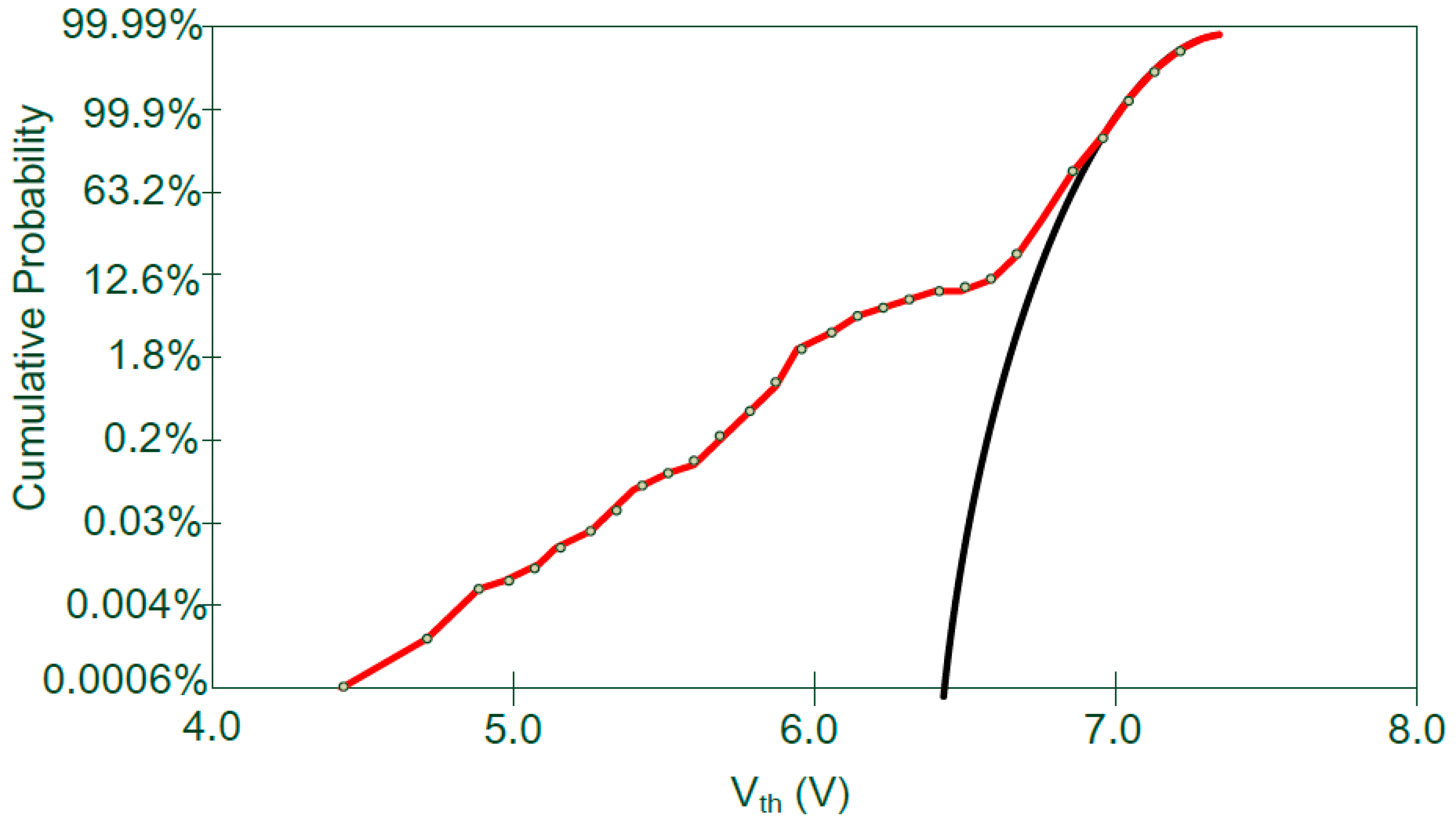
Figure 1 shows one of the results in [
1]. Read only memory (ROM) is a semiconductor memory. Its characteristics is its contents cannot be changed or erased once they have been stored in it. Moreover, its contents will not disappear in spite of power-off. It can be either Electrically-Erasable Programmable Read-Only Memory (EEPROM) or NOR FLASH in implementation. In this study, any floating-gate ROMs can match the characteristics in
Figure 1. Two ROM devices can be chosen for verification—the AT24CS of Atmel, and the S25FL128S of CYPRESS. They are popular and easily available.
According to Reference [
2],
Figure 2 specifies how reading error is caused by the shifted V
TH (ΔV
TH). When the cell’s V
TH is lower than read voltage (V
read), read error happens because status “0” is read as “1”. Status “1” does not have this side-effect, because the ΔV
TH of status “1” is almost zero according to the conclusion in Reference [
1]. Obviously, the error rates caused by radiation are different between erased cells (status “1”), and programmed cells (status “0”). In Reference [
3], a dynamic read reference voltage is used in reading data from non-volatile memory cells. The read reference voltage is calibrated. An Error Checking and Correction (ECC) algorithm is performed to identify whether errors exist in the data for read using the initial read reference voltage level. If errors in the data are identified when read, a pre-determined value is retrieved to adjust the initial read reference voltage level to a new read reference voltage level.
In this paper, a novel technology called “Variable Length Error Detection Code” (VLEDC) for the Non-Volatile Memory (NVM) protection is proposed. Although there have been some methods about variable length coding of memory protection [
4,
5], they were developed without considering the error rate difference between status “1” and status “0” in the memory content. Combined with two-dimensional parity check architecture, the proposed 2D-VLEDC can achieve a high error coverage with significant cost reduction. Compared with the traditional ECC techniques, selectivity can be made in our design to allow a user to choose either ECC or parity check according to the contents stored in ROM, thereby decreasing the required redundant bits significantly.
This paper was organized as follows: In
Section 2, how the 2D-VLEDC works and is applied to NVM is described.
Section 3 discusses the experiments on performance comparison of other methods of memory protection with our 2D-VLEDC. Concluding remarks are given in
Section 4.
2. Proposed Method
Before discussing 2D-VLEDC, we first introduce a two-dimensional parity (2D-parity) check.
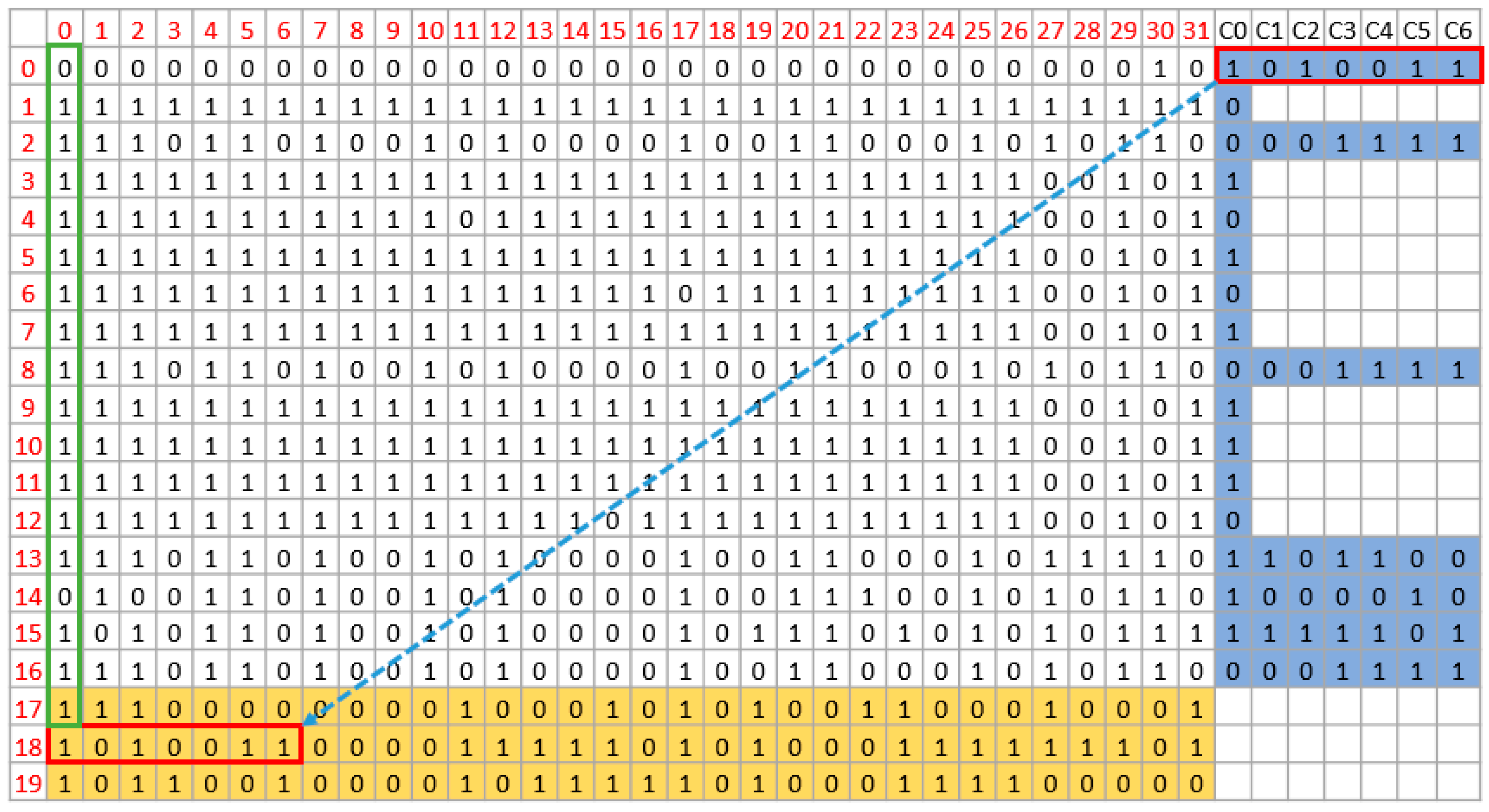
Figure 3 describes a ROM whose physical size is 20 × 32 (address 0~19, each address has 32 bits) bits as an example. The addresses from 0 to 16 contain the program codes that Central Processing Unit (CPU) runs with. It is called as data area. The C1 column is
Y-axis 1-bit parity check of data word at relative address. For example, green square (address 0) in the
Figure 3 specifies an even parity coding scheme. In the address 0, only bit (0, 30) from bit 0 to 31 equals to 1, so bit (0, C1) equals to 1. In the same way, address 17 is
X-axis 1-bit even parity bit for column bits of the program codes. As shown as blue square in the
Figure 3, there are totally 15 ones in the column 1 from address 0 to address 16, so the (17, 1) equals to 1 according to even parity rule.
To apply the 2D-parity in a typical memory, the
Y-axis parity bits (address 18) are stored in the address behind the program codes (address 0 to 16), and
X-axis parity (address 17). As shown in
Figure 3, the
Y-axis (column C1) bits are stored at the address 18 as presented in the red square. The remaining bits in the address 18 are filled with 0. The storage of
X-axis and
Y-axis is called as signature area. In addition, as shown in address 19, the same 2D-parity can be applied to the signature area again to implement self-checking-like scheme to improve the fault tolerant quality.
The 2D-parity could detect and correct single bit error in both data area and signature area. Any 2-bit error could be detected. However, the locating of two error bits is not always successful. For example, if there are two error bits in one data word, the X-axis shows no change of parity bit even two of bit changes in Y-axis parity are found—that is to say, this 2-bit error can be identified but the location of error bit cannot be found, resulting in failure to recover them. As a result, the error handling capability is named as single error correction and double error detection (SECDED).
To compare the undetected error rate of 2D-parity with ECC, a fault injection simulation was applied, as shown in
Table 1. In this simulation, 1 to 4 errors were injected and all possible error location combinations in an 8 × 32 size of ROM were evaluated. In other words, for 4-errors fault injection simulation, there are C (8 × 32, 4) operations including injecting fault, decoding, and comparison in the simulation, where C means “combination”.
Table 1 shows the results of fault injection simulation with 2D-parity and ECC. Undetected error rate equals to (undetected error counts)/C (8 × 32, 4) × 100%.
Table 1 show that 2D-parity and ECC can detect all errors from 1 to 3 errors’ fault injection. In the 4 errors’ fault injection simulation, ECC has effectiveness better (twice) than 2D-parity. The cost overhead of 2D-parity equals to ((8 + 32)/(8 × 32)) × 100% = 15.625%. The cost of ECC equals to ((7 × 8)/(8 × 32)) × 100% = 21.875%. 2D-parity overhead/ECC overhead = 71.43%.
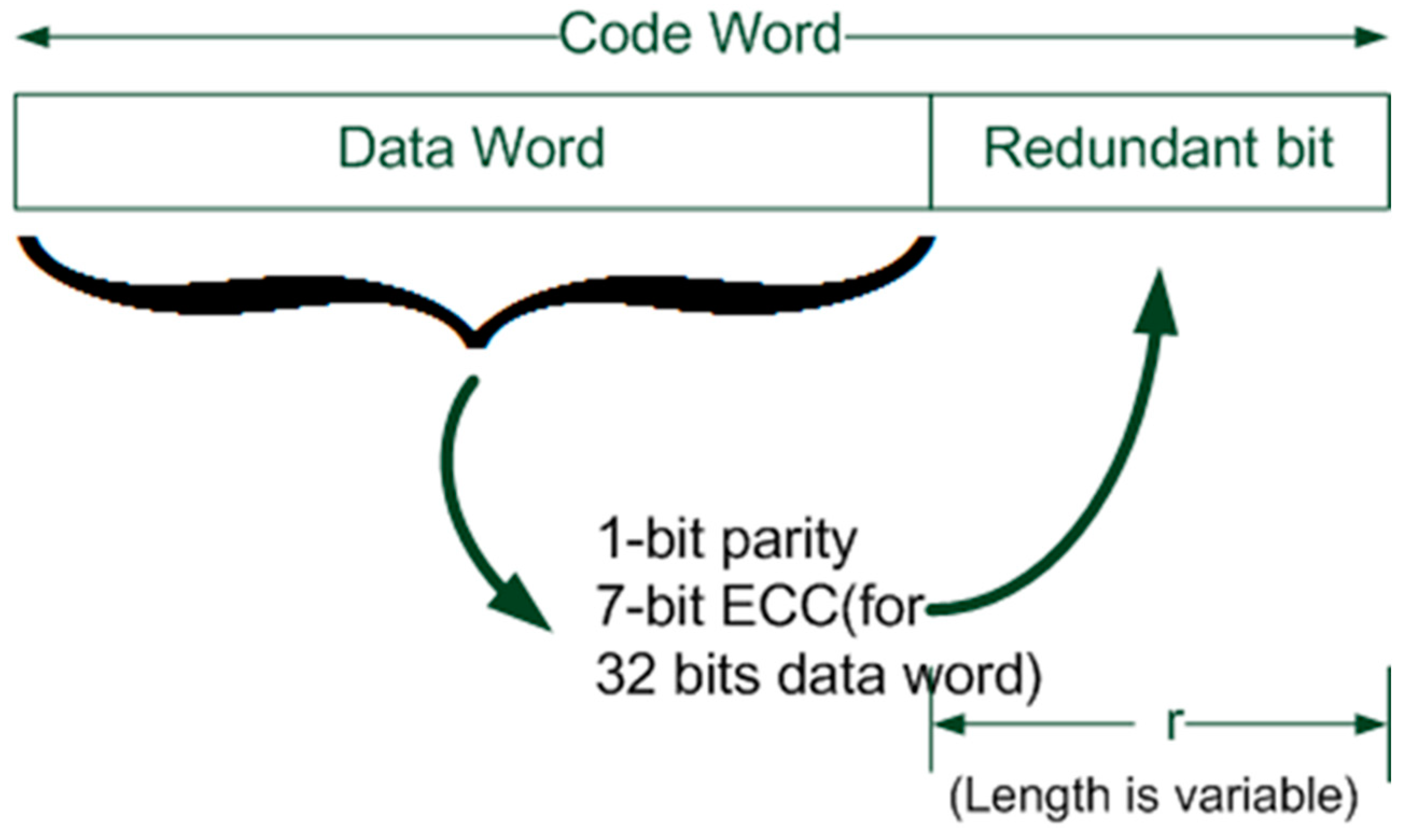
One possible way to improve the error detection rate of 2D parity is to include ECC on data word to replace the
X-axis parity. However, it induces significant increase in redundancy. Here an idea of variable length error detection code is proposed. The probability of read error between 1-to-0 and 0-to-1 is different after NVM in the radiation. It was taken into account to select appropriate
X-axis redundancy.
Figure 4 shows the concept of our VLEDC, the content of data word decides the method of encoding with respective redundant bits. As a result, the length of redundant bits is variable for each data word in NVM.
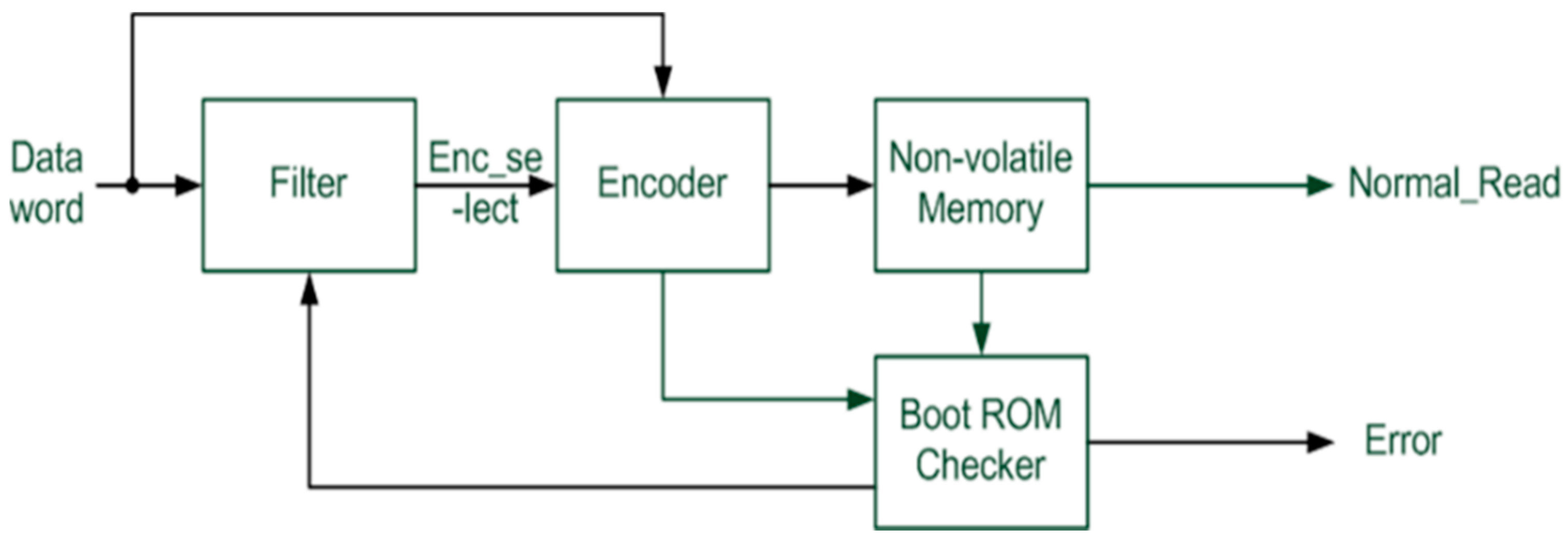
Figure 5 shows the architecture of the proposed 2D-VLEDC, including: Filter, encoder, boot checker and NVM modules. The encoder includes several known memory protection technologies, like 1-bit parity and 7-bits ECC. Before encoding data word, filter module generates encoder-selecting signals by analyzing the zero counts in the data word. A few filter rules could be applied for the filter, such as the number of zero count, the consecutive zero bits, and so on. These threshold values of rule, such as the number of “0” bits, could be adjusted according to the demands of reliability in the system.
The same as those in the 2D-parity, the generated redundant bits are stored in the signature area.
Figure 6 shows that the redundant bits are stored at the addresses from No. 21 to No. 22 as marked in the red box. Address 20 stores the
Y-axis parity bits. For example, the bit-0 of data word in the address 20 is equal to XOR all bit-0 from address 0 to address 16 as presented in the green box. That is even parity check for all bit-0 from address 0 to address 16.
Before CPU boots up, Boot ROM checker module first performs the boot ROM checking. Boot ROM checker module reads data word, sends data word to filter module to perform encoding process again and finally compares the redundant bit in the NVM with re-calculated ones. If the results of the identical comparison are true, CPU will fetch instructions normally. If the results of the comparison are false, Boot ROM checker module will alarm an error signal to external interface.
3. Experiments
This section illustrates an experiment to evaluate the performance of the proposed 2D-VLEDC. The performance comparison between other methods of memory protection and 2D-VLEDC are given.
Table 2 shows the filer rule applied to the experiments. One-bit parity was applied to those data words with less than half of content is “0”. The 7-bit ECC was applied to those data words with more than half of content is “1”. As shown in
Table 2, the 1-bit parity is used when the number of “0” is 0–15 in an address date. On the other hand, a 7-bit ECC is applied to the system when the number of “0” becomes 16–31.
3.1. Experiment Flow
The experiments were exercised with different ROM sizes from 8 × 32, 16 × 32, 32 × 32, 64 × 32, 128 × 32, to 256 × 32. For each ROM size, 100 trials are exercised, and each trial runs 10
6 times of fault injection and error detection evaluation. The flow chart of the provided experiments is shown in
Figure 7 and described step by step as follows:
Step 1. Specify ROM size and target simulation times (sim_times). The parameter “sim_times” is defined as 106 times here.
Step 2. Repeat step 3 to step 9 100 times, and go to step 10.
Step 3. Generate a random content of ROM.
Step 4. Based on generated random content in the step 3, generate the encoding results as golden patterns of 1-bit parity, 2D parity, 7-bits ECC and 2D-VLEDC.
Step 5. Repeat step 6 to step 8 106 times, and go to step 9.
Step 6. Inject four random errors into the ROM randomly.
Step 7. Perform the decoding flow of 1-bit parity, 2D parity, 7-bits ECC and 2D-VLEDC with the injected-errors ROM.
Step 8. Check error detection of each decoding result. Accumulate the number of un-detected errors into the un-detected error counter and then go to step 4.
Step 9. Log undetected error rate (Rate
ud) and size overhead of each memory protection technology in the log-files. Go to step 2.
Step 10. Analyze 95% confidence interval from the log-files.
Step 11. Finish experiment.
Therefore, there are 100 Rateud data for each ROM size with 1-bit parity, 2D parity, 7-bits ECC and 2D-VLEDC.
3.2. Performance Comparison
The result of analyzing 95% confidence level interval with 100 Rate
ud data for each ROM size are shown in the
Table 3. In the
Table 3, “Margin of Error” = 1.96 × σ/n
0.5. “StdDev” is the abbreviation of “Standard Deviation”. “UDR” is the abbreviation of “Un-Detected error Rate”. Each “Average”, “StdDev” and “Margin of Error” value comes from the 100 trials, and each trial has 10
6 fault injection simulations. From the 10
6 fault injection simulations, the Rate
ud (UDR in the
Table 3) from the Equation (1) can be obtained.
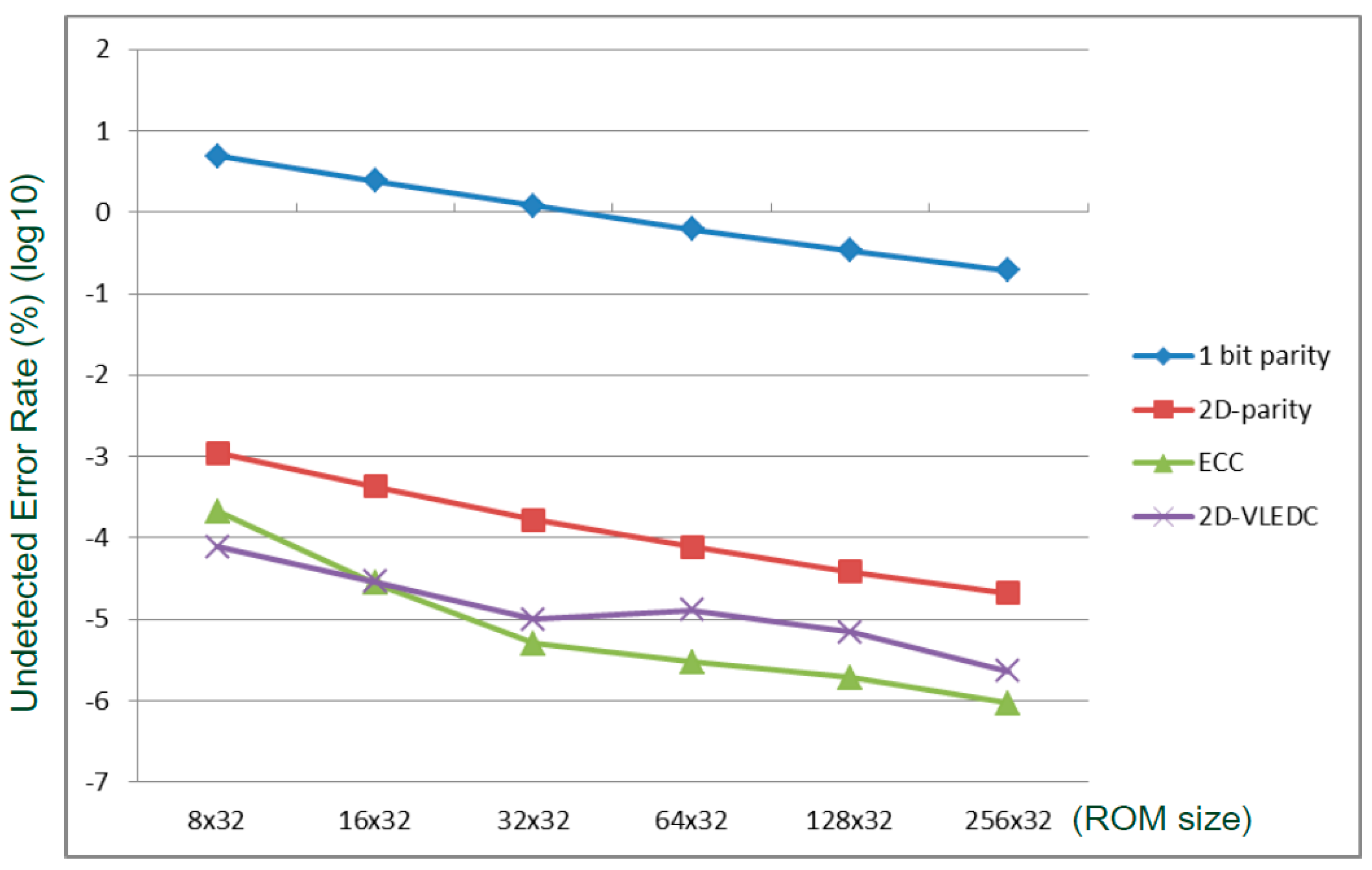
Figure 8 shows the undetected error rate of each methodology versus ROM size. The point of the value in the
Figure 8 is the field of “Average” in the
Table 3 with the process of log
10. 2D-VLEDC has better performance at the ROM size 8 × 32. With the growing of the ROM size, ECC is getting better performance than the 2D-VLEDC. However, the error detection performance has no significant difference between them.
Figure 9 shows the size overhead of each methodology versus ROM size. It was calculated by the Equation (2). The overhead of 2D-parity gradually reduces and approaches the overhead size of the 1-bit parity with the growing of the ROM size. 2D-VLEDC has approximate 10 times improvement in error coverage rate over the 2D-parity, but pays for 10~12% overhead. The results show that 2D-VLEDC needs 15% redundancy while ECC needs 22% redundancy in average. The 2D-VLEDC has not only the improvement of error coverage rate that approximates the coverage of ECC but also has 30% less overhead than the ECC’s. For address of
n, the required worst-case and best-case redundant bits are 7
n and
n, respectively, under the 2D-VLEDC.

 ,
, 


