A Modular Cell Balancer Based on Multi-Winding Transformer and Switched-Capacitor Circuits for a Series-Connected Battery String in Electric Vehicles


Abstract
:1. Introduction
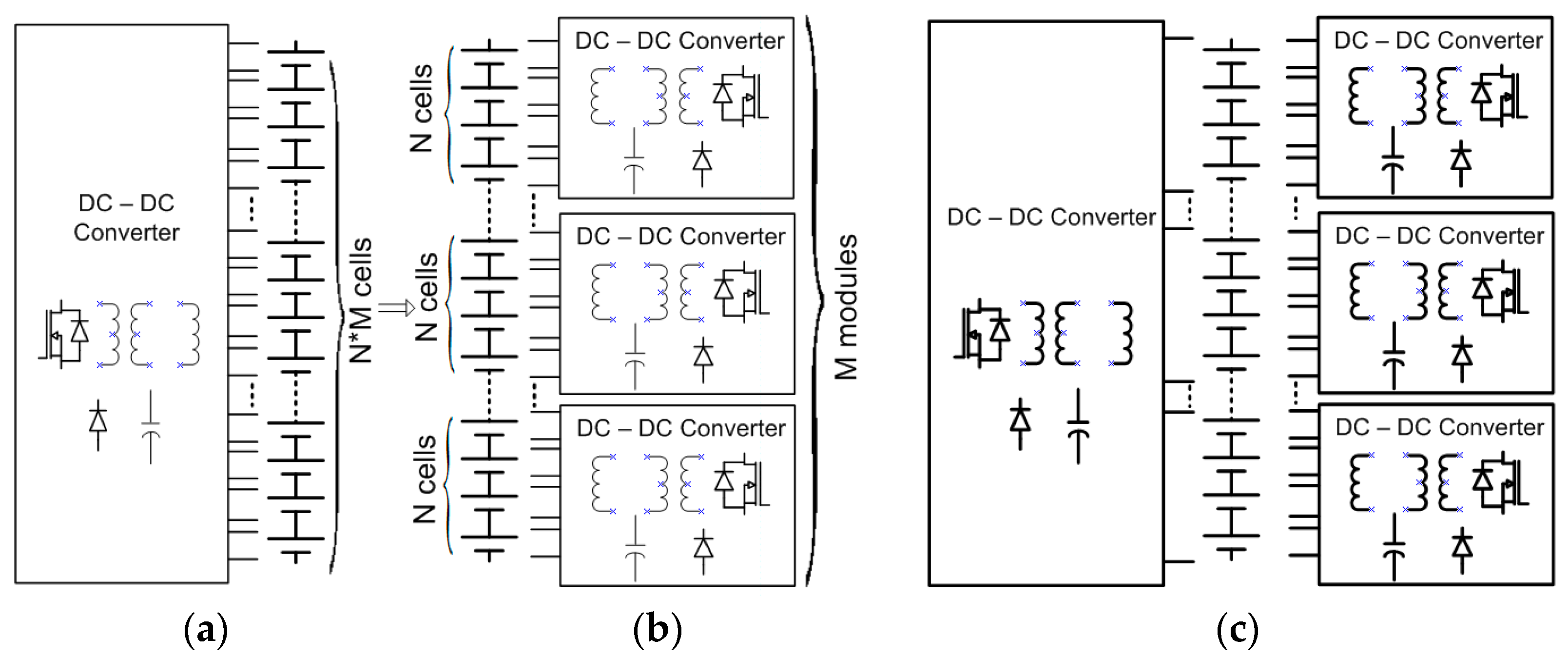
2. Proposed Modular Cell Balancing Circuit
2.1. Analysis of the Previous Cell Balancing Circuits
2.1.1. Active Cell Balancing Circuit Using the MWT
2.1.2. Cell Balancing Circuit Using SCC
2.2. Proposed Modular Cell Balancing Circuit
2.2.1. Modular Cell Balancing Concept
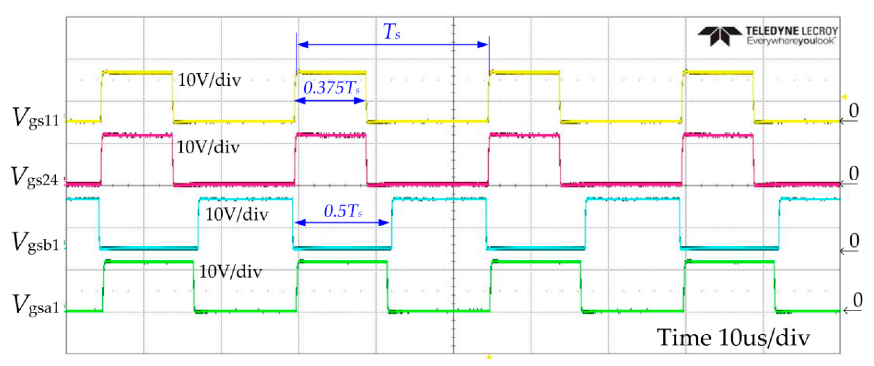
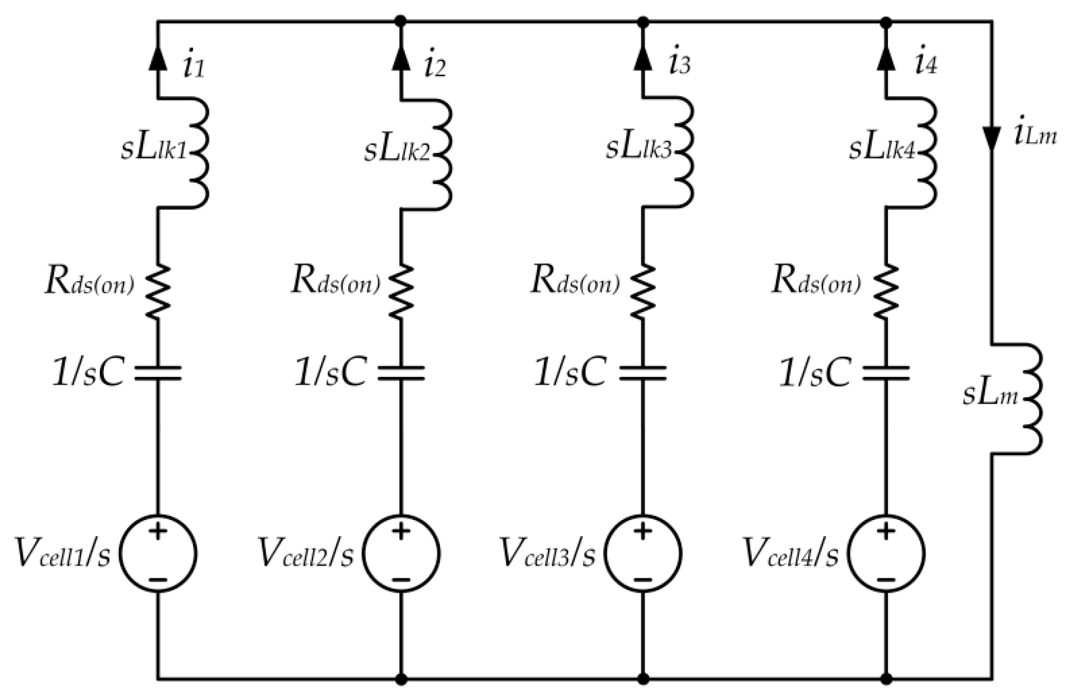
2.2.2. Proposed Modular Cell Balancing Circuit
- All the switches, capacitor, diodes and transformer are ideal.
- Each module contains four cells.
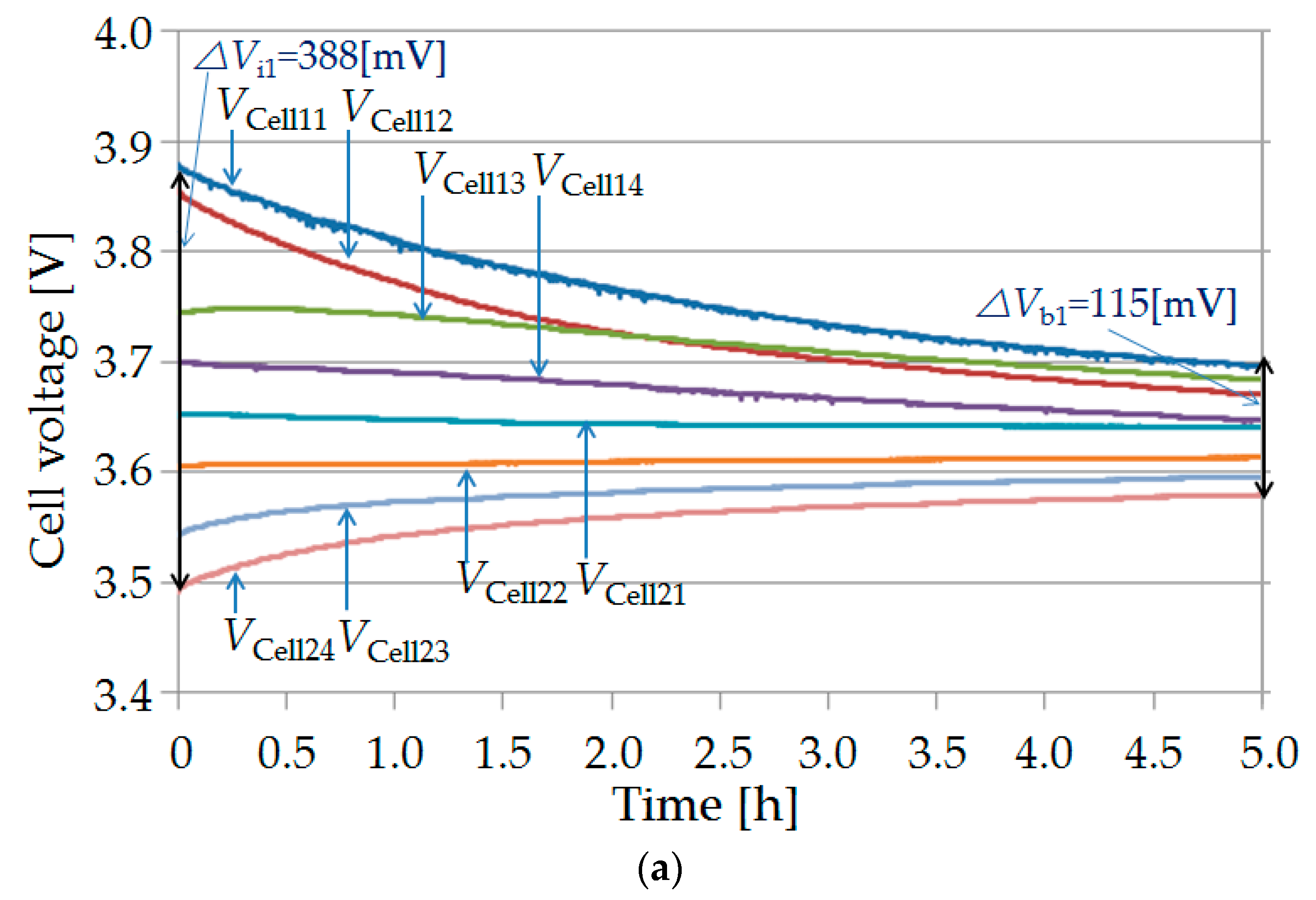
- The relationship among voltage of the battery cells is arranged in decreasing order from Cell11 (Vcell11) to Cell24 (Vcell24), and Vcell11 > Vcell12 > Vaver1 > Vcell13 > Vcell14 > Vcell21 > Vcell22 > Vaver2 > Vcell23 > Vcell24 (the module 1 voltage: VM1 = VCell11 + VCell12 + VCell13 + VCell14; the average voltage of M1: Vaver1 = VM1/4; the module 2 voltage: VM2 = VCell21 + VCell22 + VCell23 + VCell24; the average voltage of M2: Vaver2 = VM2/4; VM1 > VM2).
3. Experimental Setup
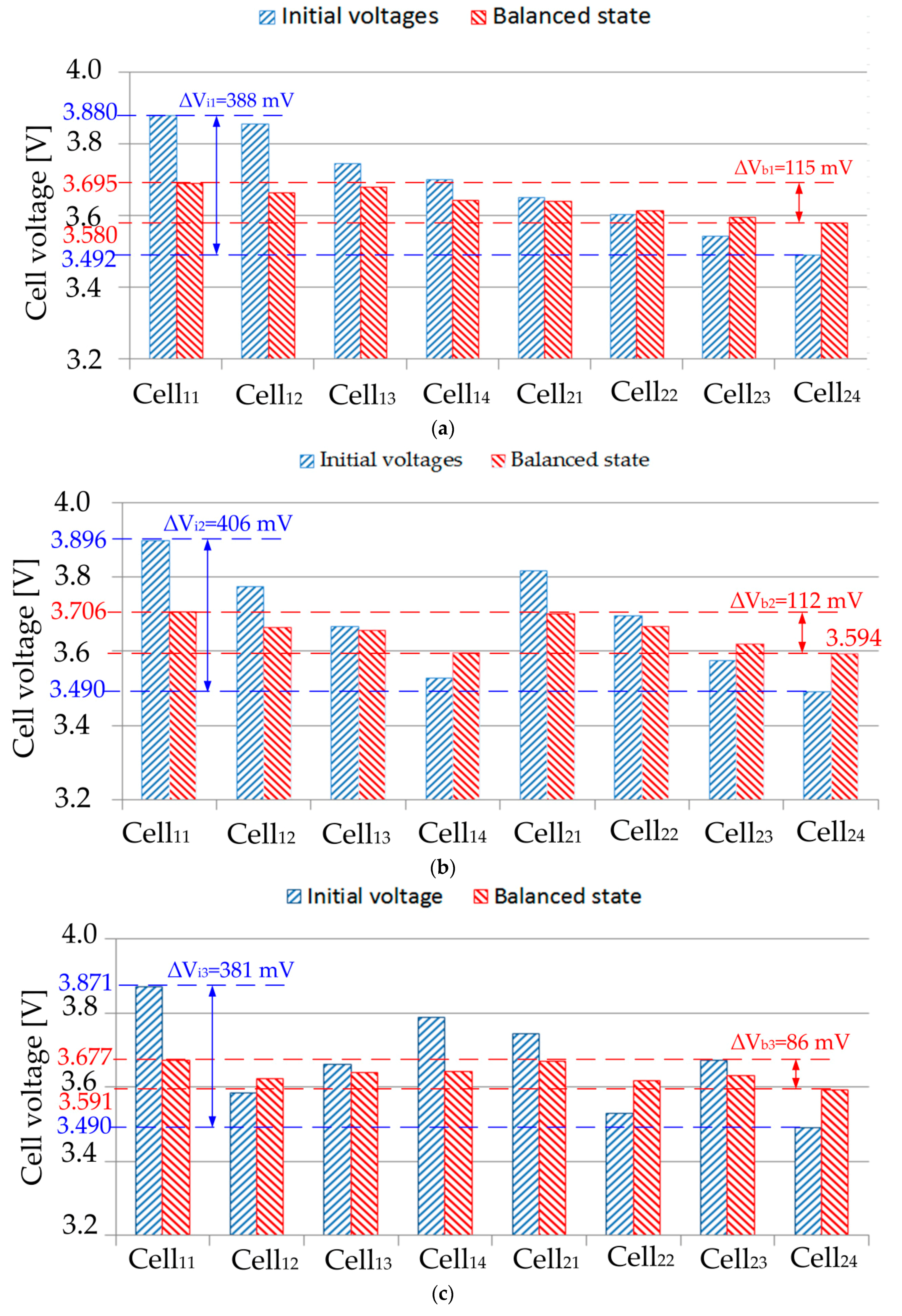
4. Results and Discussion
5. Comparison with Conventional Balancing Methods
- Basically, the proposed balancing circuit has some advantages originally found in the MWTFC-based balancer and SCC-based balancer such as the repudiation of the voltage sensors for the feedback control loop, simple control scheme.
- The MWTFC-based balancer is applied to a small number of cells. Therefore, the problem of mismatched leakage inductance can be minimized.
- The voltage stress of switches is low by applying the SCC-based balancer to the outer-module balancer.
- The number of cells in series can be easily extended.
6. Conclusions
Author Contributions
Funding
Acknowledgments
Conflicts of Interest
Nomenclature
| Cell | battery cell |
| C | capacitance |
| D | duty cycle |
| i | current |
| L | inductance |
| S | MOSFET |
| V | Balancing capacitor voltage |
| Ts | switching period |
| Subscripts | |
| aver | average |
| cb | balancing capacitor |
| cm | module capacitor |
| ch | charge |
| dis | discharge |
| ds | drain-source |
| eq | equivalent |
| gs | gate-source |
| m | magnetic |
| min | minimum |
| PP | transformer’s primary |
| TS | transformer’s secondary |
| Acronyms | |
| C | Capacitor |
| D | Diode |
| DSP | Digital Signal Processor |
| EV | electric vehicle |
| HEV | Hybrid electric vehicle |
| IC | Integrated circuit |
| M | Module |
| MCBC | Modular cell balancing circuit |
| MWT | Multi-winding transformer |
| MWTFC | MWT forward converter |
| NTC | Negative Temperature Coefficient |
| PWM | Pulse-Width-Modulated |
| SCBS | Series-connected Lithium-Ion battery string |
| SCC | Switched capacitor circuit |
| T | Transformer |
References
- Kim, C.H.; Kim, M.Y.; Moon, G.W. A modularized charge equalizer using a battery monitoring ic for series-connected li-ion battery strings in electric vehicles. IEEE Trans. Power Electron. 2013, 28, 3779–3787. [Google Scholar] [CrossRef]
- Kim, C.; Member, S.; Kim, M.; Member, S.; Park, H.; Member, A.; Moon, G. A Modularized Two-Stage Charge Equalizer With Cell Selection Switches for Series-Connected Lithium-Ion Battery String in an HEV. IEEE Trans. Power Electron. 2012, 27, 3764–3774. [Google Scholar] [CrossRef]
- Park, H.; Member, S.; Kim, C.; Kim, C.; Member, S.; Moon, G.; Lee, J. A Modularized Charge Equalizer for an HEV Lithium-Ion Battery String. IEEE Trans. Ind. Electron. 2009, 56, 1464–1476. [Google Scholar] [CrossRef]
- Allègre, A.L.; Bouscayrol, A.; Delarue, P.; Barrade, P.; Chattot, E.; El-Fassi, S. Energy storage system with supercapacitor for an innovative subway. IEEE Trans. Ind. Electron. 2010, 57, 4001–4012. [Google Scholar] [CrossRef]
- Panchal, S.; Mathew, M.; Dincer, I.; Agelin-Chaab, M.; Fraser, R.; Fowler, M. Thermal and electrical performance assessments of lithium-ion battery modules for an electric vehicle under actual drive cycles. Electr. Power Syst. Res. 2018, 163, 18–27. [Google Scholar] [CrossRef]
- Panchal, S.; Dincer, I.; Agelin-Chaab, M.; Fowler, M.; Fraser, R. Uneven temperature and voltage distributions due to rapid discharge rates and different boundary conditions for series-connected LiFePO4batteries. Int. Commun. Heat Mass Transf. 2017, 81, 210–217. [Google Scholar] [CrossRef]
- Lee, Y.; Jeon, S.; Lee, H.; Bae, S. Comparison on cell balancing methods for energy storage applications. Indian J. Sci. Technol. 2016, 9. [Google Scholar] [CrossRef]
- Daowd, M.; Omar, N.; van den Bossche, P.; van Mierlo, J. A review of passive and active battery balancing based on MATLAB/Simulink. Int. Rev. Electr. Eng. 2011, 6, 2974–2989. [Google Scholar] [CrossRef]
- Bentley, W.F. Cell balancing considerations for lithium-ion battery systems. Twelfth Annu. Batter. Conf. Appl. Adv. 1997, 223–226, 223–226. [Google Scholar] [CrossRef]
- Bui, T.; Bae, S. Active Clamped Forward based Active Cell Balancing Converter. Indian J. Sci. Technol. 2015, 8, 1–6. [Google Scholar] [CrossRef]
- Ye, Y.; Cheng, K.W.E. An automatic switched-capacitor cell balancing circuit for series-connected battery strings. Energies 2016, 9, 138. [Google Scholar] [CrossRef]
- Wu, T.H.; Moo, C.S.; Hou, C.H. A battery power bank with series-connected buck-boost-type battery power modules. Energies 2017, 10, 650. [Google Scholar] [CrossRef]
- Imtiaz, A.M.; Khan, F.H. “Time shared flyback converter” based regenerative cell balancing technique for series connected li-ion battery strings. IEEE Trans. Power Electron. 2013, 28, 5960–5975. [Google Scholar] [CrossRef]
- Zeltser, I.; Kirshenboim, O.; Dahan, N.; Peretz, M.M. ZCS resonant converter based parallel balancing of serially connected batteries string. In Proceedings of the 2016 IEEE Applied Power Electronics Conference and Exposition (APEC), Long Beach, CA, USA, 20–24 March 2016. [Google Scholar]
- Pascual, C.; Krein, P.T. Switched capacitor system for automatic series battery equalization. In Proceedings of the APEC 97—Applied Power Electronics Conference, Atlanta, GA, USA, 27 February 1997. [Google Scholar]
- Kim, M.Y.; Kim, C.H.; Kim, J.H.; Moon, G.W. A chain structure of switched capacitor for improved cell balancing speed of lithium-ion batteries. IEEE Trans. Ind. Electron. 2014, 61, 3989–3999. [Google Scholar] [CrossRef]
- Jeon, S.; Kim, M.; Bae, S. Analysis of a symmetric active cell balancer with a multi-winding transformer. J. Electr. Eng. Technol. 2017, 12, 1812–1820. [Google Scholar] [CrossRef]
- Kim, J.W.; Ha, J.I. Cell balancing method in flyback converter without cell selection switch of multi-winding transformer. J. Electr. Eng. Technol. 2016, 11, 367–376. [Google Scholar] [CrossRef]
- Stuart, T.; Zhu, W. Fast equalization for large lithium ion batteries. IEEE Aerosp. Electron. Syst. Mag. 2009, 24, 27–31. [Google Scholar] [CrossRef] [Green Version]
- Kim, J.; Ha, J. Cell Balancing Control of Single Switch Flyback Converter Using Generalized Filters. In Proceedings of the 29th Annual IEEE Applied Power Electronics Conference and Exposition–APEC 2014, Fort Worth, TX, USA, 16–20 March 2014. [Google Scholar]
- Hoque, M.M.; Hannan, M.A.; Mohamed, A.; Ayob, A. Battery charge equalization controller in electric vehicle applications: A review. Renew. Sustain. Energy Rev. 2017, 75, 1363–1385. [Google Scholar] [CrossRef]
- Ling, R.; Wang, L.; Huang, X.; Dan, Q.; Zhang, J. A review of equalization topologies for lithium-ion battery packs. In Proceedings of the 34th Chinese Control Conference, Hanzhou, China, 28–30 July 2015. [Google Scholar]
- Caspar, M.; Eiler, T.; Hohmann, S. Comparison of active battery balancing systems. In Proceedings of the 2014 IEEE Vehicle Power and Propulsion Conference (VPPC), Coimbra, Portugal, 27–30 October 2014. [Google Scholar]
- Shang, Y.; Xia, B.; Zhang, C.; Cui, N.; Yang, J.; Mi, C.C. An Automatic Equalizer Based on Forward-Flyback Converter for Series-Connected Battery Strings. IEEE Trans. Ind. Electron. 2017, 64, 5380–5391. [Google Scholar] [CrossRef]
- Li, S.; Mi, C.C.; Zhang, M. A high-efficiency active battery-balancing circuit using multiwinding transformer. IEEE Trans. Ind. Appl. 2013, 49, 198–207. [Google Scholar] [CrossRef]
- Cao, J.; Schofield, N.; Emadi, A. Battery balancing methods: A comprehensive review. In Proceedings of the 2008 IEEE Vehicle Power and Propulsion Conference, Harbin, China, 3–5 September 2008. [Google Scholar]
- Hua, C.C.; Fang, Y.H. A switched capacitor charge equalizer with cancellation mechanism of alternating current. In Proceedings of the 2015 IEEE 2nd International Future Energy Electronics Conference (IFEEC), Taipei, Taiwan, 1–4 November 2015. [Google Scholar]
- Lim, C.S.; Lee, K.J.; Ku, N.J.; Hyun, D.S.; Kim, R.Y. A modularized equalization method based on magnetizing energy for a series-connected lithium-ion battery string. IEEE Trans. Power Electron. 2014, 29, 1791–1799. [Google Scholar] [CrossRef]
- Kanade, S.A.; Puri, V. Electrical properties of thick-film NTC thermistor composed of Ni0.8Co0.2Mn2O4ceramic: Effect of inorganic oxide binder. Mater. Res. Bull. 2008, 43, 819–824. [Google Scholar] [CrossRef]
- Daowd, M.; Antoine, M.; Omar, N.; van den Bossche, P.; van Mierlo, J. Single switched capacitor battery balancing system enhancements. Energies 2013, 6, 2149–2179. [Google Scholar] [CrossRef]
- Ji, X.; Cui, N.; Shang, Y.; Zhang, C.; Sun, B. Modularized charge equalizer using multiwinding transformers for Lithium-ion battery system. In Proceedings of the 2014 IEEE Conference and Expo Transportation Electrification Asia-Pacific (ITEC Asia-Pacific), Beijing, China, 31 August–3 September 2014; pp. 1–5. [Google Scholar] [CrossRef]
- Chen, H.; Zhang, L.; Han, Y. System-theoretic analysis of a class of battery equalization systems: Mathematical modeling and performance evaluation. IEEE Trans. Veh. Technol. 2015, 64, 1445–1457. [Google Scholar] [CrossRef]
- Zhang, Z.; Gui, H.; Gu, D.J.; Yang, Y.; Ren, X. A hierarchical active balancing architecture for lithium-ion batteries. IEEE Trans. Power Electron. 2017, 32, 2757–2768. [Google Scholar] [CrossRef]
- Park, H.-S.; Kim, C.-H.; Park, K.-B.; Moon, G.-W.; Lee, J.-H. Design of a charge equalizer based on battery Modularization. IEEE Trans. Veh. Technol. 2009, 58, 3216–3223. [Google Scholar] [CrossRef]
- Uno, M.; Kukita, A. Modular equalization architecture using inter-module and switchless intra-module equalizer for energy storage system. In Proceedings of the 17th European Conference on Power Electronics and Applications, Geneva, Switzerland, 8–10 September 2015. [Google Scholar]
- Ling, R.; Dan, Q.; Wang, L.; Li, D. Energy bus-based equalization scheme with bi-directional isolated Cuk equalizer for series connected battery strings. In Proceedings of the 2015 IEEE Applied Power Electronics Conference and Exposition (APEC), Charlotte, NC, USA, 15–19 March 2015. [Google Scholar]
- Park, S.H.; Kim, T.S.; Park, J.S.; Moon, G.W.; Yoon, M.J. A new battery equalizer based on buck-boost topology. In Proceedings of the 7th Internatonal Conference on Power Electronics, ICPE’07, Daegu, Korea, 22–26 October 2007; pp. 962–965. [Google Scholar]
- Lee, Y.S.; Cheng, G.T. Quasi-resonant zero-current-switching bidirectional converter for battery equalization applications. IEEE Trans. Power Electron. 2006, 21, 1213–1224. [Google Scholar] [CrossRef]


| Parameter | Value | ||
|---|---|---|---|
| Cell balancing circuit | Twelve MOSFETs | IPP023N10N5 | |
| Two diodes | DO-204AC (DO-15) | ||
| Two Transformers (Four primary/One secondary windings) | Core: EER2828N | ||
| N1:N2 = 1:1 | |||
| Lm1 = 1.88 mH; Lm2 = 1.83 mH | |||
| Llk11 = 1.87 µH; Llk12 = 1.95 µH; Llk13 = 3.39 µH; Llk14 = 1.94 µH; Llk21 = 2.30 µH; Llk22 = 1.99 µH; Llk23 = 2.00 µH; Llk24 = 1.98 µH; | |||
| Balancing capacitor | 700 µF | ||
| Gate driver | UCC27519A-Q1 | ||
| Battery string | Eight Lithium-ion cells | Nominal capacity | 700 mAh |
| Nominal voltage | 3.7 V | ||
| Weight | 18 g | ||
| Cell voltage recorder | Series-connected cell string recorder | YOKOGAWA-GP10 | |
| Controller | Switching frequency | 40 kHz | |
| Digital controller | TMS320F28335 | ||
| Case 1 | Case 2 | Case 3 | ||||
|---|---|---|---|---|---|---|
| Battery Cells | Initial Cell Voltages [V] | Module Voltage [V] | Initial Cell Voltages [V] | Module Voltage [V] | Initial Cell Voltages [V] | Module Voltage [V] |
| Cell11 | 3.880 | VM1 = 15.183 | 3.896 | VM1 = 14.862 | 3.871 | VM1 = 14.906 |
| Cell12 | 3.857 | 3.773 | 3.585 | |||
| Cell13 | 3.745 | 3.666 | 3.661 | |||
| Cell14 | 3.701 | 3.527 | 3.789 | |||
| Cell21 | 3.652 | VM2 = 14.291 | 3.816 | VM2 = 14.575 | 3.744 | VM2 = 14.437 |
| Cell22 | 3.604 | 3.695 | 3.529 | |||
| Cell23 | 3.543 | 3.574 | 3.674 | |||
| Cell24 | 3.492 | 3.490 | 3.490 | |||
| V∑Cell [V] | 29.474 | 29.437 | 29.343 | |||
| Topology | No. of the Components | |||||
|---|---|---|---|---|---|---|
| Switch | D | C | L | Transformer | ||
| Switched capacitor converter | Basic SCC [22] | 2n | - | n − 1 | - | - |
| Double-Tiered SCC [26] | 2n | - | 2n − 3 | - | - | |
| Single SCC [30] | n + 5 | - | 1 | - | - | |
| Quasi-Resonant SCC [38] | 2n | - | n − 1 | n − 1 | - | |
| Buck-boost Converter | Basis topology [12] | 2(n − 1) | - | - | n − 1 | - |
| Cuk converter [36] | 2(n − 1) | - | n − 1 | 2(n − 1) | - | |
| Multi-winding transformer | Flyback converter [18] | 1 | n | - | - | 1 (n primary windings) |
| Forward converter [17] | n | 1 | - | - | 1 (n primary windings) | |
| Proposed topology | n + 2M | M | M − 1 | - | M (n/M primary windings) 1 | |
© 2018 by the authors. Licensee MDPI, Basel, Switzerland. This article is an open access article distributed under the terms and conditions of the Creative Commons Attribution (CC BY) license (http://creativecommons.org/licenses/by/4.0/).
Share and Cite
Bui, T.M.; Kim, C.-H.; Kim, K.-H.; Rhee, S.B. A Modular Cell Balancer Based on Multi-Winding Transformer and Switched-Capacitor Circuits for a Series-Connected Battery String in Electric Vehicles. Appl. Sci. 2018, 8, 1278. https://doi.org/10.3390/app8081278
Bui TM, Kim C-H, Kim K-H, Rhee SB. A Modular Cell Balancer Based on Multi-Winding Transformer and Switched-Capacitor Circuits for a Series-Connected Battery String in Electric Vehicles. Applied Sciences. 2018; 8(8):1278. https://doi.org/10.3390/app8081278
Chicago/Turabian StyleBui, Thuc Minh, Chang-Hwan Kim, Kyu-Ho Kim, and Sang Bong Rhee. 2018. "A Modular Cell Balancer Based on Multi-Winding Transformer and Switched-Capacitor Circuits for a Series-Connected Battery String in Electric Vehicles" Applied Sciences 8, no. 8: 1278. https://doi.org/10.3390/app8081278