Discharge Characteristics and Plasma Erosion of Various Dielectric Materials in the Dielectric Barrier Discharges

1
Department of Electrical and Biological Physics, Kwangwoon University, 20 Kwangwoon-Ro, Nowon Wallgye, Seoul 01897, Korea
2
Department of Chemistry, Kwangwoon University, 20 Kwangwoon-Ro, Nowon Wallgye, Seoul 01897, Korea
*
Author to whom correspondence should be addressed.
Appl. Sci. 2018, 8(8), 1294; https://doi.org/10.3390/app8081294
Submission received: 9 April 2018
/
Revised: 30 May 2018
/
Accepted: 31 July 2018
/
Published: 3 August 2018
(This article belongs to the Special Issue Polymers, Copolymers, Block Copolymers and Nanoparticles)
Abstract
:The objective of this study is the investigation of dielectric barrier discharges (DBDs) with the solid plates and the flexible polymer films. A high capacitance with a high dielectric constant and a small thickness is responsible for the discharge of a high plasma current with a low operation voltage; here, the thin flexible polyimide film ensured a high capacitance, and is comparable to the thick solid-plate alumina. In the long-duration test of the dielectric-surface plasma erosion, the solid plates show a high resistance against the plasma erosions, while the polymer films are vulnerable to the etching by the plasma-species chemical reaction. The polymer-film surface, however, was reinforced remarkably against the plasma erosion by the silicone-paste coating.
1. Introduction
The nonthermal atmospheric-pressure plasmas (NTAPP) have been studied for their applications in the various fields of the ozone synthesis, surface modification, plasma chemistry, and biomedicine, including the skin cosmetics, skin diseases, and wound healing [1,2,3,4,5,6,7,8,9,10]. The NTAPP-using plasma jets and the dielectric barrier discharge (DBD) devices have been reported in the biomedical field [11,12,13,14,15,16]. A plasma jet is generated by the applying of a high voltage to the end electrode of the gas injector. The discharge gas in the plasma jets is used for various gases such as the inert gas [17,18,19,20], nitrogen gas (N2), air [12,21,22,23,24,25], and mixtures thereof [26,27,28]. In the DBD devices, the plasma is generated on the surface of the dielectric layer by the applying of a high voltage to the electrode enclosed in the dielectric layer. The two plasma types generated in the DBD devices are as follows: The human-skin floating electrode as the ground electrode [4,6], and the plasma generated in the dielectric layer corresponding to the high-voltage electrode around the ground electrode [29,30,31,32].
Since the first DBD experiments were reported by Siemens [7] in 1857, DBDs have been known for more than a century [33,34]. Quartz and alumina have been used as the dielectrics of the DBD devices [5,6,7]. The polymer film has also been considered for the DBD-device application. It is easy to handle the flexible polymer films regarding various geometric-structure forms due to their flexibilities. In addition, since the film dielectric layer is made as thinly as possible, the discharge voltage could be reduced, and this is advantageous for the DBD-device fabrication. Recently, the flexible polymer films have been used to manufacture a flexible plasma pad that can be applied for the wearable DBDs, such as the patches, bands, hats, and socks [35,36].
In this study, the discharge properties of various dielectric materials with thin solid plates and thin flexible films were examined regarding the DBD devices, with an especial focus on the plasma-discharge plasma erosion on the dielectric surface. The results of this study demonstrate that, for the DBD dielectric-layer application, the polymer films are vulnerable to the plasma erosion. The advantageous results of the reinforced silicone (Si) coating on the polymer films against the plasma erosion are described.
2. Materials and Methods
The glass, quartz, and alumina solid plates and the flexible polymer films were used as the dielectric materials for the experimental samples. The polyimide (PI), polypropylene (PP), and glass polymer (GP) were used as the dielectric materials of the flexible polymer films. Table 1 lists the information on the dielectric materials used in this experiment. Since the solid plates are fragile, they are limited to thickness reductions of less than several-hundred μm. An alkaline earth boro-aluminosilicate wafer served as the glass in the experiment. Synthetic quartz was used in this study. The purity of the alumina-ceramic substrate is 99.9%. The thinnest solid plate among the commercially available ones is of the 500-μm thickness (T). The dielectric constant K values are 9.0, 5.3 and 3.6 for the alumina, glass, and quartz, respectively. The selection of the samples of the flexible polymer film is based on the commercially available film thicknesses. For the PI, GP and PP, the T values are 125 μm, 200 μm and 300 μm, respectively, while the K values are 2.8, 3.0 and 2.3, respectively. The T of the selected PI is the thickest among the commercial products. The GP film is equivalent to the smartphone-display protection film. In the flexible films, the dielectric thickness is different for each sample; accordingly, the capacitance (C~K/T) of each sample was affected by the K and T values.
The PI-film properties include a high heat resistance, an excellent flexibility, and the resistance to chemicals and combustion [37]. The PI was developed for the aerospace industry in 1964 (DuPont Kapton®). The PI film cannot be deformed over a wide range of temperatures, ranging from −269 to 400 °C, but it has been widely used as the substrate of the flexible printed circuit board.
The PP is an inexpensive polymer material made of carbon (C) and hydrogen (H) [38,39,40,41] that is used in a variety of fields such as packaging films, fibers, and daily goods. The PP film is prone to oxidation (or degradation) when it is exposed to heat or the ultraviolet light. The PP melting point is approximately 160 °C, so it is considered thermally weak; however, its chemical properties are excellent. The PP can withstand many organic solvents, except strong oxidizing agents.
The GP has been developed to complement vulnerabilities such as the thermal deformation of the polymer materials. It is mainly used in the liquid-crystal protective films of the mobile phones and displays. In this experiment, the test sample film is SILPLUS® (H Global, Brooklyn, NY, USA).
In Figure 1, the various DBD types introduced in [33,34] were tested for the discharge-ignition experiments with the dielectric layer of the alumina-ceramic plate, as follows: spatial discharge between the face-to-face electrodes in (a), the coplanar discharge in (b), and the planar discharges between the both-side electrodes in (c-i)–(c-iv). The electrodes were coated with copper to 40-μm in thickness. All the experiments were performed in the atmospheric environment.
In Figure 2, with the various dielectric materials listed in Table 1, a dielectric-barrier surface discharge was investigated for the discharge properties, current voltage, and firing voltage. The DBD structure shown in Figure 1c-iii was chosen, which is proper for the bio-medical application of the wearable plasma devices [35,36]. The plasma erosion of the dielectric surface was also tested. The damage and deformation on the dielectric surface were observed in a prolonged discharge test. The functional groups present in the infrared (IR) spectra of the PP- and PI-surface films in the absence or presence of the plasma were measured using the MB3000 Fourier transform IR spectroscopy device (ABB Bomen, Zurich, Switzerland).
Figure 2 shows the schematic diagram of the discharge experiment in the atmospheric environment. An annular-shaped ground electrode was attached to the dielectric upper surface, and a high-voltage circular-shaped electrode was attached to the lower surface. The electrodes were coated with copper (Cu) of the T = 40 μm. The outer and inner diameters of the annular-shaped electrode are 15 mm and 5 mm, respectively. The diameter of the circular-shaped electrode is 5 mm. The high-voltage electrode coincides with the ground-electrode inner circle. The high-voltage electrodes were insulated by the insulation pads attached onto the dielectric lower surface. A long-term discharge experiment was then conducted to assess the durability of the dielectrics.
A high voltage from 0.5 to 3.0 kV was applied to the electrodes with the direct current (dc)–alternating current (ac) inverter. The voltage is the sinusoidal signal with the frequency of 40 kHz. The high voltage was measured using the P6015A high-voltage probe (Tektronix, Beaverton, OR, USA), and the current was measured using the Tektronix P6022A ac probe. The voltage and current signals were observed using the Tektronix DPO 4034 digital oscilloscope. All the data of current and voltage are expressed as the root-mean-square (rms) value in all the experiments.
3. Results and Discussion
From the discharge experiments shown in Figure 1 and Figure 2, the resultant discharge properties are presented in Section 3.1, the dielectric-surface plasma erosion is described in Section 3.2, and the plasma-erosion analysis is in Section 3.3.
3.1. Discharge Characteristics
The ignition (electric-breakdown or discharge-firing) test is presented in Figure 3 and Figure 4, while the electrode arrangements of the planar DBDs are shown in Figure 1 with the alumina dielectric plate. The gap distance is an essential parameter for the ignition along the discharge path between the metallic electrodes on the surface of the dielectric layer. Figure 5 and Figure 6 with the various dielectric materials listed in Table 1 show the discharge mode and the current–voltage (I–V) characteristics, respectively, while the DBD structure of Figure 2 is applicable for the actual plasma pads [35,36].
For the DB discharge between the face-to-face electrodes in Figure 1a, Figure 3 shows the spatial-discharge photographs in (a) and the Paschen curve in (b) according to the spatial gap distance d between the upper electrode and the dielectric-layer surface. The dielectric layer is the alumina ceramic with the T = 0.5 mm in thickness and the copper electrodes are W = 10 mm in width and L = 30 mm in length. The upper electrode was applied to a high voltage and the lower electrode was grounded. For the discharge ignition with the proposed-inverter output voltage in the range of 0.5–3.0 kV, the d of this experiment is from 0.1 to 0.5 mm. The firing voltage Vf = 0.99–1.76 kV corresponding to the d = 0.1–0.5 mm and the Pd = 7.7–38.0 (Torr cm) for the P = 760 Torr. The firing voltage Vf and the current were measured three times and averaged within an error range of less than 5%, and the firing voltage was plotted in Figure 3b. The data of the gap distance, firing voltage, and current are (d, Vf, I) = (0.1 mm, 0.99 kV, 5.5 mA), (0.2 mm, 1.16 kV, 4.7 mA), (0.3 mm, 1.35 kV, 4.5 mA), (0.4 mm, 1.53 kV, 4.4 mA), and (0.5 mm, 1.76 kV, 4.2 mA). As the d was increased, the Vf increased for the Paschen breakdown while the current decreased, even for the increasing of the brightness intensity of the visual plasma.
Considering the decreasing current, the amount of the displacement current that can be passed through the dielectrics and the real current (plasma current other than the capacitive type) were determined. It was expected the displacement current would be high for the high capacitance of the short gap, and therefore the total current increased to a high value for the short gap, while the total current for the long gap is low, even though it was expected the plasma current would be high with the high Vf for the long gap. From the Paschen data of Figure 3b, it can be interpolated that the Vf is ~21 kV for the d = 1 cm, together with the reported operating voltage of the same order as that of the earlier atmospheric DBD experiments where the Pd is ~760 Torr cm [33,34].
In the coplanar discharge of Figure 1b, which is the typical structure of the microdischarge in the plasma display panel (PDP), the ignition was not observed with the alumina plate of the T = 0.5 mm in this experiment. With the proposed inverter in the output-voltage range of 3 kV, the insulation breakdown occurred between the two electrodes of the short gap d < 1 mm, and the ignition on the dielectric-layer surface did not occur for the d > 1 mm. As a result, the coplanar discharge cannot be ensured unless the dielectric layer is quite thin. In the case of the microdischarge PDP with the dielectric-layer thickness of less than 100 µm, the reported ignition voltage is approximately 300 V for the low-pressure values of less than a few tens of Torr. Therefore, the DBD atmospheric discharge is not suitable for the coplanar discharge.
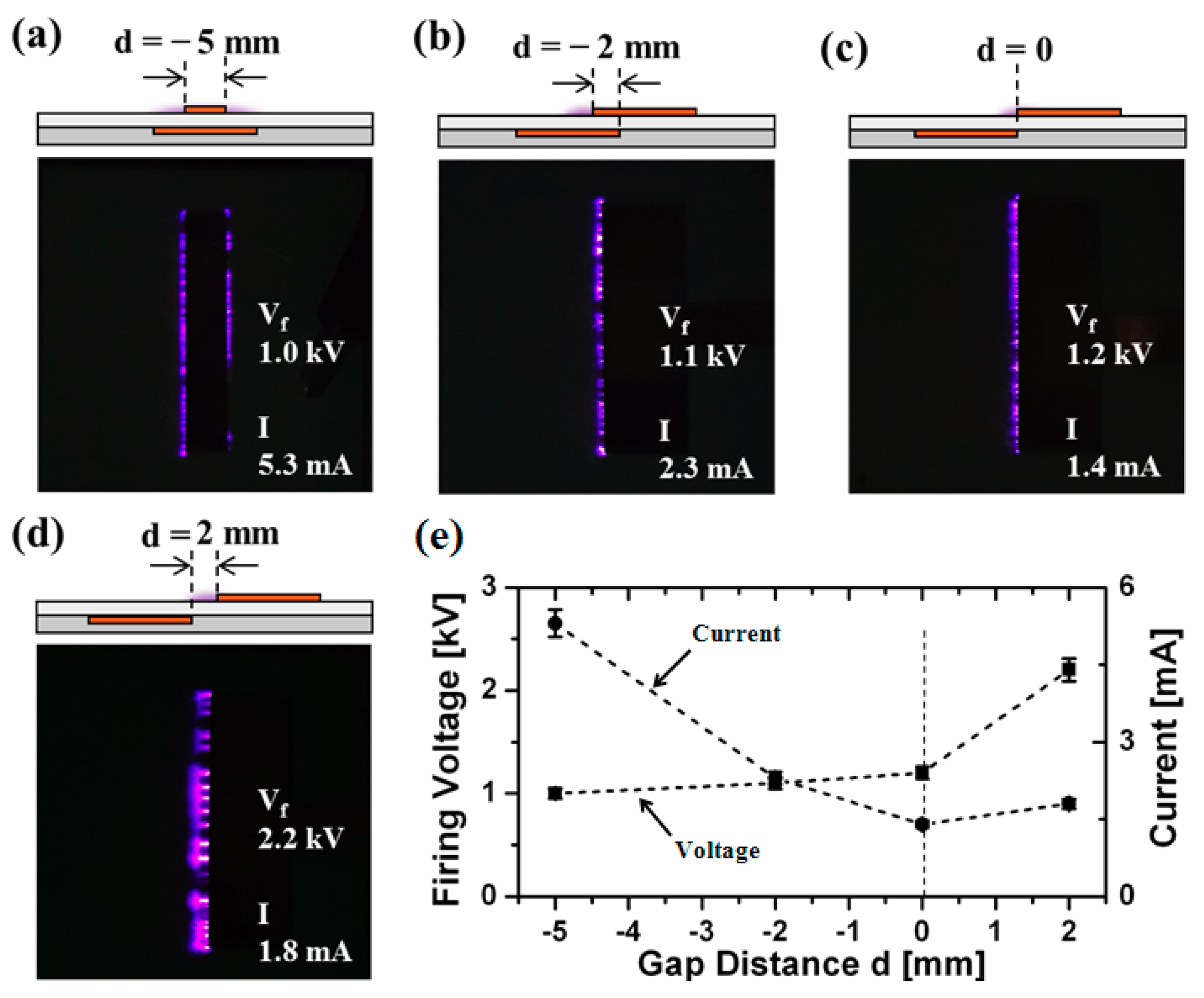
The ignition tests with the planar discharge of Figure 1c are shown in Figure 4. Two electrodes are both sides of the dielectric layer (alumina ceramic) with the T = 0.5 mm. A high voltage was applied to the lower electrode covered with the insulation pad, and the ground was applied to the upper electrode. All the electrodes are 10-mm wide and 30-mm long, except the upper electrode of the 5-mm width, as shown in Figure 4a. All the data of ignition voltage Vf and current were measured three times and averaged as shown in Figure 4a–d and as plotted in Figure 4e within an error range of less than 5%. The negative value of gap distance d means the overlapped electrode. The upper electrode is overlapped as d = −5 mm over the center of the lower electrode in Figure 4a, where the Vf = 1.0 kV and the current is I = 5.3 mA for both the plasma-generated upper-electrode sides. In Figure 4b with the overlapped electrodes of d = −2 mm at the edge, the Vf = 1.1 kV and the current is I = 2.3 mA. In Figure 4c with the d = 0 between the two electrodes, the ignition voltage is Vf = 1.2 kV and the current is I = 1.4 mA. In Figure 4d with the d = 2 mm, the Vf = 2.2 kV and the current is I = 1.8 mA. With the overlapped electrodes of (a) and (b), the Vf is low while the current is high, since the displacement current is high for the high capacitance between the overlapped electrodes. Comparing the d = 0 in (c) with the d = 2 mm in (d), the Vf for the d = 2 mm is approximately two times higher than that for the d = 0. Further, for the wide-gap distance of d = 2 mm in (d), the discharge is unstable and the plasma is nonuniform on the discharge surface. With the wider d of > 3 mm, the ignition will not occur in the range of 3 kV with respect to the proposed inverter power system. Therefore, the d = 0 is proper in terms of the planar DBD. Thus, the structure of Figure 1c-iii was chosen for the following experiment, shown in Figure 2, for the bio-medicine application.
In Figure 3, Figure 4 and Figure 5, the shape of the discharge mode represents the multichannels of the streamer discharge that typically appear in the DBD [33,34]. Figure 5 shows the photographs of the discharges on the surface of the glass sample of Table 1 from the experiment shown in Figure 2. The plasma generation occurred on the dielectric surface over the high-voltage electrode with the 5-mm diameter. As shown in Figure 5a, the plasma was generated at the boundary line between the high-voltage and ground electrodes. As the current and voltage were increased, the plasma was observed throughout the overall boundary of both the electrodes, as shown in Figure 5b,c. The discharge was gradually enlarged to the center of the surface of the high-voltage electrode, as shown in Figure 5d,e.
Figure 6 presents the typical I–V characteristics, the so-called filamentary mode [33,34,42,43], in terms of the typical DBD operation with the atmospheric pressure. Since the capacitance is so high between the two short-gap electrodes on the surface of the both-side dielectric layer, a high displacement current is expected even before the ignition with an operation voltage less than the Vf. At the breakdown, the plasma current that is due to the filamentary channels of the microdischarges is added to the displacement current; however, the plasma current is restricted by the dielectric layer and the current will not rise abruptly. Thus, at the Vf, the slightly increasing current slope reflects the plasma generation. Under the special operating conditions, usually those of a low-pressure operation, the glow mode is present [42,43]. The latter cases of the I–V characteristics have been analyzed regarding the usual discharge-tube experiments, including the DBD structure with the gases of a low pressure that is approximately several tens of Torr [44,45,46,47]. At the breakdown voltage, the electron avalanche is accompanied by the Townsend discharge, which is the abrupt current increase followed by the normal glow in terms of the I–V characteristics. Regarding the DBD experiments of Figure 3, Figure 4 and Figure 5, however, the representation of the filamentary mode of the streamer channel is shown in Figure 6.
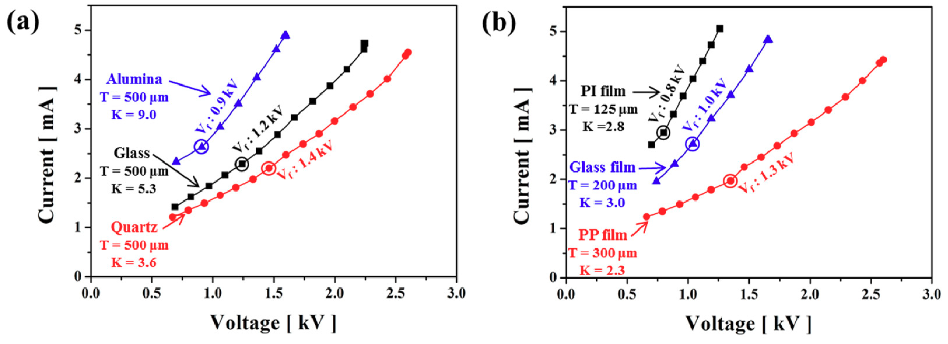
Figure 6 shows the I–V curves of each dielectric sample listed in Table 1 with respect to the discharge experiment shown in Figure 2. Figure 6a shows the graph of the solid plates and Figure 6 (b) shows the graph of the flexible films. For the electrode structure in Figure 2 with the thickness of each dielectric listed in Table 1, the capacitance was measured using the LCR-821 LCR meter (GW Instek, Taiwan), and the following results were given: (alumina, glass, quartz) = (2.40, 2.20, 1.70 pF), and (PI, GP, PP) = (2.55, 2.32, 1.70 pF). The firing voltage (Vf) is represented in the graph of Figure 6. For the Vf, the voltage was selected upon the initial observation of the plasma with the naked eye. For all the solid plates and flexible polymer films, the larger C values correspond to the greater reductions of the firing voltage and the plasma current.
For the analysis of the I–V graphs of Figure 6, the equivalent circuit is presented in Figure 7. Two circuit paths were used for the I–V measurement, as follows: One is the capacitor (Co) circuit between the electrodes of the upper and lower plates, and the other is the circuit connecting the dielectric-layer capacitance (C1) and the plasma resistance (Rp). The equivalent circuit shown in Figure 7 is composed of a parallel connection with two circuits. The impedance (Z) of the two parallel circuits is as follows [48,49]:
The slope of the I–V curve in Figure 6 corresponds to the |1/Z| of Equation (1). Assuming the sufficient largeness of the Rp (Rp > |1/ωC1|), and without considering the imaginary capacitance, the slope of the I–V curve is as follows:
In the I–V curve of Figure 6, the slope tends to change slightly before and after the discharge. The slope slightly increased after the discharge. This finding means the slope of Equation (2) increased as the Rp decreased due to the post-discharge current increase. Using Equation (2) with the reactance of the Co, the Rp was calculated for the slope value of the I–V curve in Figure 6 for each dielectric sample. The reactance (Xo = 1/ωCo) with the LCR-meter-measured Co values was calculated as follows: (alumina, glass, quartz) = (1.84, 1.90, 2.47 MΩ) and (PI, GP, PP) = (1.78, 1.87, 2.47 MΩ). Using the Xo, the Rp before and after the discharge was calculated by the comparison of the slope of the I–V curve in Figure 6 with the |1/Z| of Equation (3). The calculated pre-discharge Rp values of each sample are as follows: (alumina, glass, quartz) = (527, 680, 920 kΩ) and (PI, GP, PP) = (294, 441, 1053 kΩ). The post-discharge Rp values were reduced, as follows: (alumina, glass, quartz) = (313, 407, 490 kΩ) and (PI, GP, PP) = (217, 298, 536 kΩ).
According to the result of the equivalent-circuit analysis, the slope of the I–V curve was given by Equation (2) as |1/Z| ≈ ωCo in the low-current region before the discharge. However, after the discharge, it presented the high-current region where the Rp decreased as the slope was increased. The capacitive reactance (Xc = 1/ωCo) at the low current (2–3 mA) before the discharge is several MΩ. The Rp is in the range from several-hundred kΩ to MΩ. After the discharge, the Rp became as low as several-hundred kΩ with the current values of more than 3 mA. This Rp is in the order of several-hundred kΩ for the DBD discharge with the discharge voltage of approximately 1 kV and the current of several mA.
3.2. Plasma Erosion on the Dielectric Surfaces
Figure 8 shows the surface degradation of the dielectric samples during the prolonged operation. Figure 8a shows an enlarged photograph of the post-discharge solid-plate surface. The dotted line of the photograph shows the boundary line between the high-voltage electrode and the ground electrode. The surface was damaged on the inner surface of the dotted line due to the plasma generation. The operating-condition current of each solid plate is approximately 3 mA (V = 1.0 kV for alumina, V = 1.6 kV for glass, and V = 2.0 kV for quartz), as shown in the graph of Figure 6a. The damage on the solid-plate dielectric surface is barely apparent, even after the long operating run of 10 h. A very clean solid-plate surface was maintained after the discharge, even for the alumina, showing a slight yellow discoloring on the plasma-generation boundary surface. The solid plates, however, did not show the dielectric breakdown or the surface degradation.
Figure 8b is an enlarged photograph of the polymer-film surface after the long-run discharge. The operating-condition current of the polymer-film sample is also approximately 3 mA, as shown in Figure 6b, where the operating voltage is 0.9 kV for the PI, 1.2 kV for the GP, and 2.0 kV for the PP. On the surface of the polymer film, a severe plasma-erosion was observed. The plasma erosion caused persistent damage on the film surface and the dielectric breakdown on the damaged surface. After 19 min of the PP-film discharge operation, the dielectric breakdown occurred and the film-surface damage was observed. The erosion pattern on the PP-film surface is deep and clear. The PP film is vulnerable to the surface damage and the dielectric breakdown since the PP heat resistance is low.
The dielectric breakdown occurred in the PI film after 30 min of the operation. The pinhole appeared due to the dielectric breakdown on the PI film. The GP film did not show the dielectric breakdown even after the operation lasted for more than 10 h; however, a slight crack and the plasma erosion were also observed on the GP surface.
For the purpose of preventing the plasma erosion in Figure 8c, the polymer film was reinforced by the Si-paste coating on the film surface. The KE-441K Si paste (Shinetsu, Tokyo, Japan) was used. Since the Si chemical resistance is high, the coating prevents the plasma degradation and erosion and enhances the durability of the flexible polymer film, even for the PP film. On the surface of the polymer films coated with the Si paste of the thickness of approximately 40 μm, the erosion and dielectric breakdown did not occur, even after the long-run 10-h operation, as shown in Figure 8c. In the case of the Si-coated polymer films, however, the film surfaces were not degraded even after 10 h of the operation.
3.3. Plasma-Erosion Analysis
In the long-time discharge test results of Figure 8, the PP failed even for the short-time operation of approximately 19 min; the PI withstood 30 min of the operation. However, the Si-reinforced films did not show the plasma erosion. The weakness of the polymer films against the plasma erosion might be affected by the chemical reaction to the air plasmas. It is currently unclear whether the plasma erosion ensures the structural change of the polymer chain. The etched patterns on the film surfaces, however, seem to be due to the chemical reactions with the plasma ions and radicals.
To explicate the damages of the polymer film-surface, the IR spectroscopy was performed [50,51]. Prior to the experiments, the film to be measured was completely dried. The spectra were recorded in the range from 4500–500 cm−1 with the spectral resolution of 1.0 cm−1. Each spectrum is the average of 16 scans with the detector gain of 1.00.
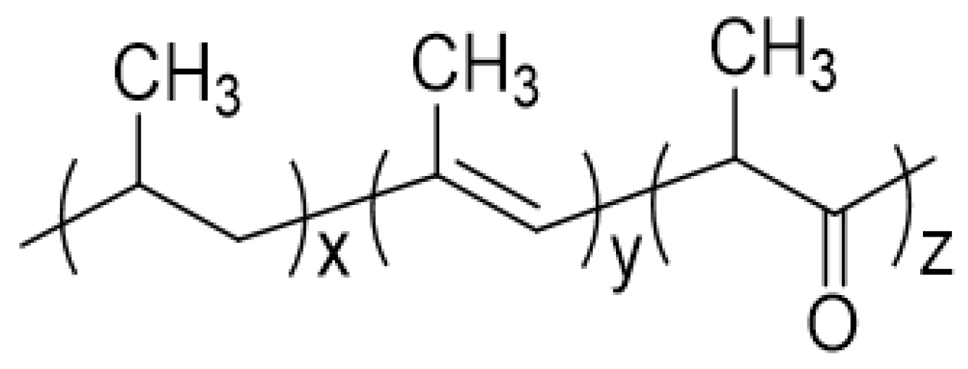
The IR spectra of the PP-surface film in the absence or presence of the plasma discharge are shown in Figure 9. The new absorption bands of the damaged-PP film that are between 1720 and 1580 cm−1 might be due to the C=C and C=O stretching vibrations and the CH bending vibrations. The broad band at approximately 1720 cm−1 is related to the C=C and C=O stretching vibrations [51]. From these new absorption bands of the damaged-PP film compared with those of the original PP-surface film in Table 1, the structural change of the PP chain could be due to the plasma discharge on the PP film, as shown in Figure 10.
To explicate the damages of the PI-film surface, the IR spectroscopy was performed, and the results are shown in Figure 11. The IR spectra of the PI-surface film in the absence or presence of the plasma discharge are shown. There were no new absorption bands regarding the PI-surface film with the plasma discharge compared with the original PI-surface film, as shown in Figure 11. This finding suggests that the structural change of the PI with the plasma discharge is not due to the rigid polymer back-bond structure such as the aromatic heterocyclic ring in the polymer main chain.
In addition, there were no new absorption bands regarding the reinforced-Si-coating PI films with the plasma discharge compared with the original reinforced Si film, as shown in Figure 12. This finding suggests the absence of a chemical structural change of the reinforced-Si-coating PI films with the plasma discharge, due to the high chemical resistance and stability of the Si.
From the IR-spectra results, the PP-chain structure was changed; however, that of the PI or the Si film was not changed. The PP was severely eroded by the surface plasma. The PI was also damaged by the plasma. The Si film, however, strongly resisted the plasma erosion.
The erosion phenomena of the dielectric-film surfaces are considered according to the chemical and physical reactions of the plasma ions and radicals. In Figure 8 of the long-time discharge, the solid-plate surfaces were not damaged while the polymer-film surface showed the etched patterns. Regarding the ion-bombardment sputtering, the threshold ion energies in the range of 10–30 eV are evident for the physical sputtering [52]. These ion energies are not available since the electron and ion plasma energies of this experiment of the atmospheric-pressure discharge are in the order of 1 eV and 0.01 eV, respectively. The oxygen and nitrogen atmospheric plasmas, however, can readily chemically affect the polymer surface of the organic materials, rather than that of the inorganic solid dielectrics. Thus, the polymers can be easily etched away by the reactive oxygen and nitrogen species (RONS) in the atmospheric-pressure plasma discharge, while the oxide materials such as silica (SiO2) and aluminum oxide (Al2O3) are quite stable against the RONS. Therefore, the chemical reactions rather than the physical sputtering exerted the effects on the surface degradation.
4. Conclusions
The main parameter of the various dielectric materials for the DBD devices is the capacitance, C ∝ K/T, with the dielectric constant, K, and the thickness, T. The characteristic of the current–voltage (I–V) depends on the C, which is proportional to the slope of the I–V curve. A large C of a high K and thin T provides a low firing voltage and a high amount of the plasma current. For the solid plates with the T of 500 μm, the K of the ceramic alumina is 9.0, which is larger than that of the glass (K = 5.3) or quartz (K = 3.6). The K of the thin flexible polymer films is ≈(2~3), which is smaller than those of the solid plates. Since the solid plates are fragile, they are limited to the thickness reduction of less than a few-hundred μm. Alternatively, the commercialized polymers are available to form the thin films with the T of less than 100 μm and with a high C, and this is achieved by reducing the film T. Therefore, the C = 2.55 pF with the K = 2.8 and the T = 125 μm is comparable to that of the alumina with the C = 2.40 pF, the K = 9, and the T = 500 μm.
In the prolonged tests involving the discharge samples, the solid plates remained strong against the plasma erosion, while the polymer films were readily etched by the chemical reaction of the air-plasma species. The glass polymer (GP) film is somewhat stronger than the polymer film; however, its film surface was also damaged after the long-run test of 10 h. The polyimide (PI) shows the dielectric breakdown and the surface degradation after the 30-min operation. The plasma erosion of the polypropylene (PP) is serious; its film did not withstand the damage even after the short-time operation of approximately 19 min. In the IR spectra of the polymer films, the structural change pf the PP chain was observed due to the plasma; however, such a change was not found for the PI. The films coated with the Si were reinforced, and they hardly showed any plasma-erosion damage, even after the prolonged test that lasted for more than 10 h.
Author Contributions
G.C. conceived and designed the experiments; J.K. performed the experiments and wrote the manuscript; S.-j.K. and Y.-N.L. performed the experiments; I.-T.K. analyzed the data.
Acknowledgments
This work was supported in part by the Kwangwoon University under a Research Grant in 2018 and by the National Research Foundation of Korea (NRF) grant funded by the Korea government (MSIT) (NRF-2018R1A2B6008642).
Conflicts of Interest
The authors declare no conflict of interest.
References
- Heinlin, J.; Morfill, G.; Landthaler, M.; Stolz, W.; Isbary, G.; Zimmermann, J.L.; Shimizu, T.; Karrer, S. Plasma medicine: Possible applications in dermatology. J. Dtsch. Dermatol. Ges. 2010, 8, 968–976. [Google Scholar] [CrossRef] [PubMed]
- Isbary, G.; Köritzer, J.; Mitra, A.; Li, Y.F.; Shimizu, T.; Schroeder, J.; Schlegel, J.; Morfill, G.E.; Solz, W.; Zimmermann, J.L. Ex vivo human skin experiments for the evaluation of safety of new cold atmospheric plasma devices. Clin. Plasma Med. 2013, 1, 36–44. [Google Scholar] [CrossRef]
- Emmert, S.; Brehmer, F.; Hänßle, H.; Helmke, A.; Mertens, N.; Ahmed, R.; Simon, D.; Wandke, D.; Friedrichs, W.M.; Däschlein, G.; et al. Atmospheric pressure plasma in dermatology: Ulcus treatment and much more. Clin. Plasma Med. 2013, 1, 24–29. [Google Scholar] [CrossRef]
- Kalghatgi, S.U.; Fridman, G.; Fridman, A.; Friedman, G.; Clyne, A.M. Non-Thermal Dielectric Barrier Discharge Plasma Treatment of Endothelial Cells. In Proceedings of the 30th Annual International Conference of the IEEE Engineering in Medicine and Biology Society, Vancouver, BC, Canada, 20–24 August 2008. [Google Scholar]
- Helmke, A.; Hoffmeister, D.; Mertens, N.; Emmert, S.; Schuette, J.; Vioel, W. The acidification of lipid film surfaces by non-thermal DBD at atmospheric pressure in air. New J. Phys. 2009, 11, 115025–115034. [Google Scholar] [CrossRef]
- Fridman, G.; Shereshevsky, A.; Jost, M.M.; Brooks, A.D.; Fridman, A.; Gutsol, A.; Vasilets, V.; Friedman, G. Floating Electrode Dielectric Barrier Discharge Plasma in Air Promoting Apoptotic Behavior in Melanoma Skin Cancer Cell Lines. Plasma Chem. Plasma Process. 2007, 27, 163–176. [Google Scholar] [CrossRef]
- Siemens, W. Ueber die elektrostatische Induction und die Verzogerung des Stroms in Flaschendrahten. Poggendorff ’s Ann. Phys. Chem. 1857, 102, 66–122. [Google Scholar] [CrossRef]
- Eliasson, B.; Hirth, M.; Kogelschatz, U. Ozone synthesis from oxygen in dielectric barrier discharges. J. Phys. D Appl. Phys. 1987, 20, 1421–1437. [Google Scholar] [CrossRef]
- Liston, E.M.; Martinu, L.; Wertheimer, M.R. Plasma surface modification of polymers for improved adhesion: A critical review. J. Adhes. Sci. Technol. 1993, 7, 1091–1127. [Google Scholar] [CrossRef]
- Eliasson, B.; Kogelschatz, U. Nonequilibrium Volume Plasma Chemical Processing. IEEE Trans. Plasma Sci. 1991, 19, 1063–1077. [Google Scholar] [CrossRef]
- Fridman, G.; Fridman, G.; Gutsol, A.; Shekhter, A.; Vasilets, V.; Fridman, A. Applied Plasma Medicine. Plasma Process. Polym. 2008, 5, 503–533. [Google Scholar] [CrossRef] [Green Version]
- Bogle, M.; Arndt, K.; Dover, J. Evaluation of Plasma Skin Regeneration Technology in Low-Energy Full-Facial Rejuvenation. Arch. Dermatol. 2007, 143, 168–174. [Google Scholar] [CrossRef] [PubMed]
- Shashurin, A.; Keidar, M.; Bronnikov, S.; Jurjus, R.; Stepp, M. Living tissue under treatment of cold plasma atmospheric jet. Appl. Phys. Lett. 2008, 98, 181501. [Google Scholar] [CrossRef]
- Weltmann, K.-D.; Kindel, E.; Brandenburg, R.; Meyer, C.; Bussiahn, R.; Wilke, C.; von Woedtke, T. Atmospheric Pressure Plasma Jet for Medical Therapy: Plasma Parameters and Risk Estimation. Contrib. Plasma Phys. 2009, 49, 631–640. [Google Scholar] [CrossRef]
- Kim, Y.; Jin, S.; Han, G.; Kwon, G.; Choi, J.; Choi, E.; Uhm, H.; Cho, G. Plasma Apparatuses for Biomedical Applications. IEEE Trans. Plasma Sci. 2015, 43, 944–950. [Google Scholar] [CrossRef]
- Fridman, G.; Peddinghaus, M.; Ayan, H.; Fridman, A.; Balasubramanian, M.; Gutsol, A.; Brooks, A.; Friedman, G. Blood Coagulation and Living Tissue Sterilization by Floating-Electrode Dielectric Barrier Discharge in Air. Plasma Chem. Plasma Process. 2006, 26, 425–442. [Google Scholar] [CrossRef]
- Stoffels, E.; Flikweert, A.; Stoffels, W.; Kroesen, G. Plasma needle: A non-destructive atmospheric plasma source for fine surface treatment of (bio)materials. Plasma Sources Sci. Technol. 2002, 11, 383–388. [Google Scholar] [CrossRef]
- Walsh, J.; Kong, M. Room-temperature atmospheric argon plasma jet sustained with submicrosecond high-voltage pulses. Appl. Phys. Lett. 2007, 91, 221502. [Google Scholar] [CrossRef] [Green Version]
- Urabe, K.; Morita, T.; Tachibana, K.; Ganguly, B. Investigation of discharge mechanisms in helium plasma jet at atmospheric pressure by laser spectroscopic measurements. J. Phys. D Appl. Phys. 2010, 43, 095201. [Google Scholar] [CrossRef]
- Cho, G.; Kim, Y.; Uhm, H. The Jet-Stream Channels of Gas and Plasma in Atmospheric-Pressure Plasma Jets. J. Korean Phys. Soc. 2016, 69, 525–535. [Google Scholar] [CrossRef]
- Hong, Y.; Uhm, H.; Yi, W. Atmospheric pressure nitrogen plasma jet: Observation of striated multilayer discharge patterns. Appl. Phys. Lett. 2008, 93, 051504. [Google Scholar] [CrossRef]
- Deng, X.; Nikiforov, A.; Vanraes, P.; Leys, C. Direct current plasma jet at atmospheric pressure operation in nitrogen and air. J. Appl. Phys. 2013, 113, 023305. [Google Scholar] [CrossRef] [Green Version]
- Hong, Y.; Uhm, H. Air plasma jet with hollow electrodes at atmospheric pressure. Phys. Plasmas 2007, 14, 053503. [Google Scholar] [CrossRef]
- Kolb, J.; Mohamed, A.; Price, R.; Swanson, R.; Bowman, A.; Chiavarini, R.; Stacey, M.; Schoenbach, K. Cold atmospheric pressure air plasma jet for medical applications. Appl. Phys. Lett. 2008, 92, 241501. [Google Scholar] [CrossRef]
- Pei, X.; Lu, X.; Liu, J.; Liu, D.; Yang, Y.; Ostrikov, K.; Chu, P.; Pan, Y. Inactivation of a 25.5 μm Enterococcus faecalis biofilm by a room-temperature, battery-operated, handheld air plasma jet. J. Phys. D Appl. Phys. 2012, 45, 165205. [Google Scholar] [CrossRef]
- Yonemori, S.; Nakagawa, Y.; Ono, R.; Oda, T. Measurement of OH density and air-helium mixture ratio in an atmospheric-pressure helium plasma jet. J. Phys. D Appl. Phys. 2012, 45, 225202. [Google Scholar] [CrossRef]
- Shen, J.; Cheng, C.; Fang, S.; Xie, H.; Lan, Y.; Ni, G.; Meng, Y.; Luo, J.; Wang, X. Sterilization of Bacillus subtilis Spores Using an Atmospheric Plasma Jet with Argon and Oxygen Mixture Gas. Appl. Phys. Express. 2012, 5, 036201. [Google Scholar] [CrossRef]
- Sarani, A.; Nikiforov, A.; Geyter, N.; Morent, R.; Leys, C. Surface modification of polypropylene with an atmospheric pressure plasma jet sustained in argon and an argon/water vapour mixture. Appl. Surf. Sci. 2011, 257, 8737–8741. [Google Scholar] [CrossRef]
- Park, G.; Baik, K.; Kim, J.; Kim, Y.; Lee, K.; Jung, R.; Cho, G. Analysis of Biological Effects of a Non-thermal Plasma on Saccharomyses Cerevisiae. J. Korean Phys. Soc. 2012, 60, 916–920. [Google Scholar] [CrossRef]
- Ehlbeck, J.; Schnabel, U.; Polak, M.; Winter, J.; von Woedtke, T.; Brandenburg, R.; von dem Hagen, T.; Weltmann, K.-D. Low temperature atmospheric pressure plasma sources for microbial decontamination. J. Phys. D Appl. Phys. 2011, 44, 013002. [Google Scholar] [CrossRef]
- Von Woedtke, T.; Reuter, S.; Masur, K.; Weltmann, K.-D. Plasmas for medicine. Phys. Rep. 2013, 530, 291–320. [Google Scholar] [CrossRef]
- Weltmann, K.-D.; Polak, M.; Masur, K.; von Woedtke, T.; Winter, J.; Reuter, S. Plasma Processes and Plasma Sources in Medicine. Contrib. Plasma Phys. 2012, 52, 644–654. [Google Scholar] [CrossRef]
- Kogelschatz, U. Dielectric-barrier Discharges: Their History, Discharge Physics, and Industrial Applications. Plasma Chem. Plasma Process. 2003, 23, 1–46. [Google Scholar] [CrossRef]
- Wagner, H.-E.; Brandenburg, R.; Kozlov, K.V.; Sonnenfeld, A.; Michel, P.; Behnke, J.F. The barrier discharge: Basic properties and applications to surface treatment. Vacuum 2003, 71, 417–436. [Google Scholar] [CrossRef]
- Kim, Y.; Cho, H.; Kim, J.; Kim, Y.; Han, G.; Choi, E.; Cho, G. Wearable plasma-pads for healthcare applications: Plasma patch, Plasma bandage, Plasma socks, and Plasma cap. In Proceedings of the 43rd IEEE International Conference on Plasma Science, Banff, AB, Canada, 19–23 June 2016. [Google Scholar]
- Kim, J.; Choi, K.; Kim, Y.; Park, B.; Cho, G. Wearable Plasma Pads for Biomedical Applications. Appl. Sci. 2017, 7, 1308. [Google Scholar] [CrossRef]
- Liaw, D.; Wang, K.; Huang, Y.; Lee, K.; Lai, J.; Ha, C. Advanced polyimide materials: Syntheses, physical properties and applications. Prog. Polym. Sci. 2012, 37, 907–974. [Google Scholar] [CrossRef]
- Malpass, D.; Band, E. Introduction to Industrial Polypropylene: Properties, Catalysts Processes; John Wiley & Sons: New York, NY, USA, 2012; ISBN 978-1118062760. [Google Scholar]
- Kahouli, A.; Lavallee, O.G.; Rain, P.; Lesaint, O.; Heux, L.; Guillermin, C.; Lupin, J.M. Structure effect of thin film polypropylene view by dielectric spectroscopy and X-ray diffraction: Application to dry type power capacitors. J. Appl. Polym. Sci. 2015, 132, 42602. [Google Scholar] [CrossRef]
- Kahouli, A.; Lavallee, O.G.; Rain, P.; Lesaint, O.; Guillermin, C.; Lupin, J.M. Dielectric features of two grades of bi-oriented isotactic polypropylene. J. Appl. Polym. Sci. 2015, 132, 42224. [Google Scholar] [CrossRef]
- Kahouli, A.; Lesaint, O.; Lavallee, O.G.; Rain, P.; Guillermin, C. A Study of Factors and Mechanisms Responsible for the de-Metallization of Polypropylene Films Used in Dry Capacitors. In Proceedings of the 2012 IEEE Conference on Electrical Insulation and Dielectric Phenomena, Montreal, QC, Canada, 14–17 October 2012. [Google Scholar]
- Chirokov, A.; Gutsol, A.; Fridman, A.; Sieber, K.; Grace, J.; Robinson, K. A Study of Two-Dimentional Mocrodischarge Pattern Formation in Dielectric Barrier Discharges. Plasma Chem. Plasma Process. 2006, 26, 127–135. [Google Scholar] [CrossRef]
- Chirokov, A.; Gutsol, A.; Fridman, A. Atmospheric pressure plasma of dielectric barrier discharges. Pure Appl. Chem. 2005, 77, 487–495. [Google Scholar] [CrossRef]
- Kim, J.; Jeong, J.; Jin, D.; Kim, H.; Han, H.; Kwon, G.; Choi, E.; Cho, G. Longitudinal and transverse discharges with mercury-rare and xenon gases. J. Phys. D Appl. Phys. 2011, 44, 075202. [Google Scholar] [CrossRef]
- Jeong, J.; Kim, J.; Hwang, H.; Jin, D.; Koo, J.; Choi, E.; Verboncoeur, J.; Uhm, H.; Cho, G. Propagation of a Light-Emitting Wave-Front in a Fine Tube Positive Column Discharge. Jpn. J. Appl. Phys. 2010, 49, 026001. [Google Scholar] [CrossRef]
- Cho, G.; Lee, J.; Lee, D.; Kim, S.; Song, H.; Koo, J.; Kim, B.; Kang, J.; Choi, E.; Lee, U.; et al. Glow Discharge in the External Electrode Florescent Lamp. IEEE Trans. Plasma Sci. 2005, 33, 1410–1415. [Google Scholar] [CrossRef]
- Cho, T.; Kim, H.; Kim, Y.; Ko, J.; Kang, J.; Choi, E.; Cho, G.; Uhm, H. Characteristic Properties of Fluorescent Lamps Operated Using Capacitively Coupled Electrodes. Jpn. J. Appl. Phys. 2002, 41, 7518–7521. [Google Scholar] [CrossRef]
- Cho, G.; Shin, M.; Jeong, J.; Kim, J.; Hong, B.; Koo, J.; Kim, Y.; Choi, E.; Fechner, J.; Letz, M.; et al. Glass tube of high dielectric constant and low dielectric loss for external electrode fluorescent lamps. J. Appl. Phys. 2007, 102, 113307. [Google Scholar] [CrossRef]
- Reitz, J.; Milford, F.; Christy, R. Foundations of Electromagnetic Theory; Addison-Wesley Publishing Company: Boston, MA, USA, 2008; ISBN 978-0321581747. [Google Scholar]
- Thejaswini, H.C.; Peglow, S.; Sushkov, V.; Hippler, R. Infrared Spectroscopy of CH4/N2 and C2Hm/N2 (m = 2, 4, 6) Gas Mixtures in a Dielectric Barrier Discharge. Plasma Chem. Plasma Process. 2014, 34, 1157–1170. [Google Scholar] [CrossRef]
- Thejaswini, H.C.; Bogdanowicz, R.; Ruhl, E.; Danilov, V.; Meichsner, J.; Thierbach, S.; Hippler, R. Spectroscopic Study of Plasma Polymerized a-C:H Films Deposited by a Dielectric Barrier Discharge. Materials 2016, 9, 594. [Google Scholar] [CrossRef]
- Chapman, B. Glow Discharge Processes, Sputtering and Plasma Etching; John Wiley & Sons: New York, NY, USA, 1980; ISBN 978-0471078289. [Google Scholar]
Figure 1.
Schematic diagrams of the experiments with various dielectric barrier discharge (DBD) types in the atmospheric environment: (a) Spatial discharge between two parallel face-to-face electrodes; (b) coplanar discharge; and (c) planar discharges between both-side electrodes according to various arrangements at (i)–(iv).

Figure 2.
Schematic diagram of the planar-discharge experiments performed in the atmospheric environment with the various dielectric materials listed in Table 1.
Figure 2.
Schematic diagram of the planar-discharge experiments performed in the atmospheric environment with the various dielectric materials listed in Table 1.

Figure 3.
Cross-sectional pictures of the spatial discharge at the ignition voltage (Vf) according to the gap distance (d) with the dielectric barrier discharge (DBD) structure shown in Figure 1a in (a) and the Paschen curve with the firing voltage (Vf) versus the d in (b).
Figure 3.
Cross-sectional pictures of the spatial discharge at the ignition voltage (Vf) according to the gap distance (d) with the dielectric barrier discharge (DBD) structure shown in Figure 1a in (a) and the Paschen curve with the firing voltage (Vf) versus the d in (b).

Figure 4.
Pictures of the planar discharge on the dielectric surface at the ignition voltage (Vf) in the dielectric barrier discharge (DBD) structure of Figure 1c with the both-side electrodes: overlapped 5 mm at the center in (a), overlapped 2 mm at the edge in (b), no gap distance (d) = 0 in (c), and d = 2 mm in (d). And the graph of firing voltage and current versus the gap distance d in (e) where the negative value of gap distance d means the overlapped electrodes.

Figure 5.
Photographs of the discharge shapes in the dielectric barrier discharge (DBD) structure of Figure 2 in (a–e) with the increasing current and voltage on the glass-plate surface.
Figure 5.
Photographs of the discharge shapes in the dielectric barrier discharge (DBD) structure of Figure 2 in (a–e) with the increasing current and voltage on the glass-plate surface.

Figure 6.
Current–voltage (I–V) graphs for the solid plates (a) and polymer films (b).

Figure 7.
The equivalent circuit of the current–voltage measurement.

Figure 8.
Surface pictures of the solid plates after the extended-run operation (a), the flexible polymer films (b), and the reinforced-silicone (Si)-coating films (c) after the 10-h operation at the current of approximately 3 mA.
Figure 8.
Surface pictures of the solid plates after the extended-run operation (a), the flexible polymer films (b), and the reinforced-silicone (Si)-coating films (c) after the 10-h operation at the current of approximately 3 mA.

Figure 9.
Infrared (IR) spectra of the original polypropylene (PP) surface (lower black line) and the PP surface with the plasma discharge (upper red line).
Figure 9.
Infrared (IR) spectra of the original polypropylene (PP) surface (lower black line) and the PP surface with the plasma discharge (upper red line).

Figure 10.
Proposed structure of the polypropylene (PP) chain changed by the plasma discharge from the original PP structure, as shown in Table 1.
Figure 10.
Proposed structure of the polypropylene (PP) chain changed by the plasma discharge from the original PP structure, as shown in Table 1.

Figure 11.
Infrared (IR) spectra of the original polyimide (PI) surface (lower black line) and the PI surface with the plasma discharge (upper red line), showing no structural change after the plasma discharge.
Figure 11.
Infrared (IR) spectra of the original polyimide (PI) surface (lower black line) and the PI surface with the plasma discharge (upper red line), showing no structural change after the plasma discharge.

Figure 12.
Infrared (IR) spectra of the original silicone (Si) film (lower black line) and the Si PI-surface film with the plasma discharge (upper red line).
Figure 12.
Infrared (IR) spectra of the original silicone (Si) film (lower black line) and the Si PI-surface film with the plasma discharge (upper red line).


Table 1.
Formula of dielectric materials: (a) Solid plates and (b) Flexible polymer films.
| (a) | Glass | Quartz | Alumina |
| (T, K) | (500 μm, 5.3) | (500 μm, 3.7) | (500 μm, 9.3) |
| Formula | B2O3-SiO2-Al2O3 | SiO2 | Al2O3 |
| Trademark | Corning® EAGLE XG™ | Corning® 7940 Fused Silica | - |
| (b) | Polyimide (PI) | Glass Polymer (GP) | Polypropylene (PP) |
| (T, K) | (125 μm, 3.4) | (200 μm, 3.0) | (300 μm, 2.3) |
| Formula | 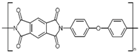 |  |  |
| Trademark | Dupont—Kapton® | H&Global—SILPLUS® | - |
© 2018 by the authors. Licensee MDPI, Basel, Switzerland. This article is an open access article distributed under the terms and conditions of the Creative Commons Attribution (CC BY) license (http://creativecommons.org/licenses/by/4.0/).
Share and Cite
MDPI and ACS Style
Kim, J.; Kim, S.-j.; Lee, Y.-N.; Kim, I.-T.; Cho, G. Discharge Characteristics and Plasma Erosion of Various Dielectric Materials in the Dielectric Barrier Discharges. Appl. Sci. 2018, 8, 1294. https://doi.org/10.3390/app8081294
AMA Style
Kim J, Kim S-j, Lee Y-N, Kim I-T, Cho G. Discharge Characteristics and Plasma Erosion of Various Dielectric Materials in the Dielectric Barrier Discharges. Applied Sciences. 2018; 8(8):1294. https://doi.org/10.3390/app8081294
Chicago/Turabian StyleKim, Junggil, Sang-jin Kim, Young-Nam Lee, In-Tae Kim, and Guangsup Cho. 2018. "Discharge Characteristics and Plasma Erosion of Various Dielectric Materials in the Dielectric Barrier Discharges" Applied Sciences 8, no. 8: 1294. https://doi.org/10.3390/app8081294
Note that from the first issue of 2016, this journal uses article numbers instead of page numbers. See further details here.