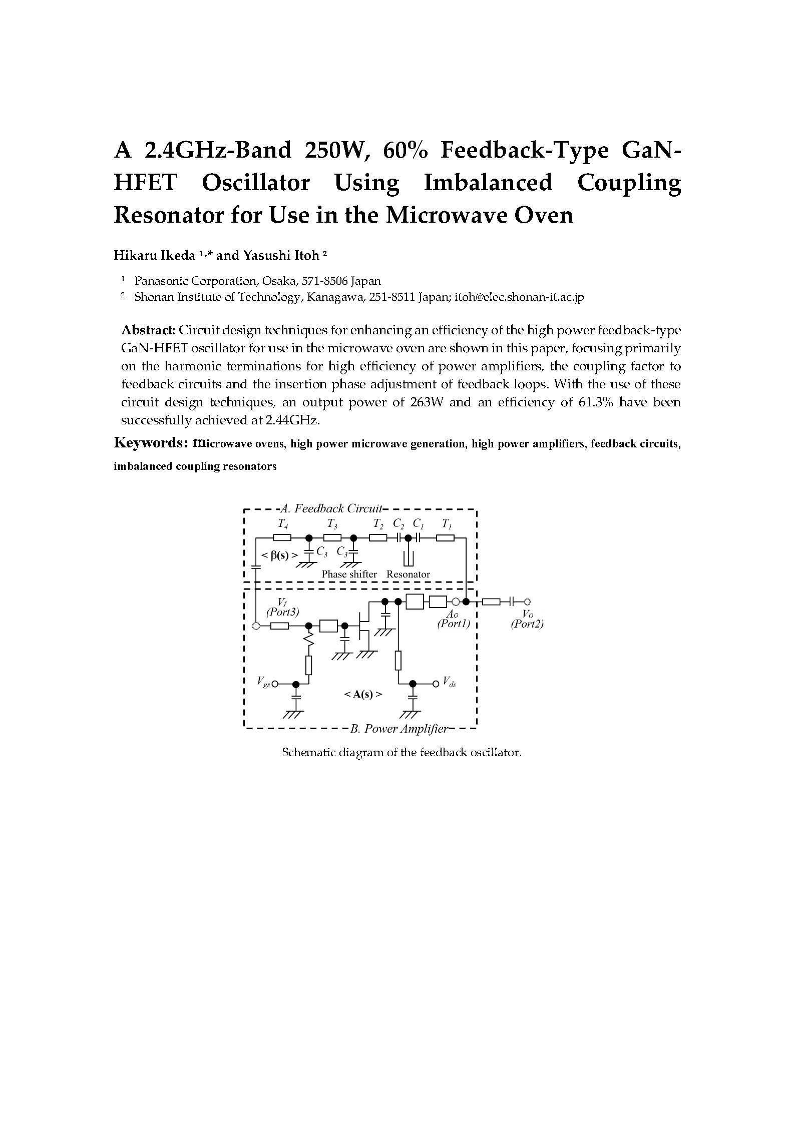
A 2.4 GHz-Band 250 W, 60% Feedback-Type GaN-HFET Oscillator Using Imbalanced Coupling Resonator for Use in the Microwave Oven

1
Industrial Solutions Company, Panasonic Corporation, Osaka 571-8506, Japan
2
Electrical and Electronics Engineering, Shonan Institute of Technology, Kanagawa 251-8511, Japan
*
Author to whom correspondence should be addressed.
Appl. Sci. 2019, 9(14), 2887; https://doi.org/10.3390/app9142887
Submission received: 22 June 2019
/
Revised: 4 July 2019
/
Accepted: 10 July 2019
/
Published: 19 July 2019
(This article belongs to the Special Issue Substrate Integrated Waveguide (SIW) and Its Applications)
Abstract
:Circuit design techniques for enhancing an efficiency of the high power feedback-type GaN-HFET (Gallium Nitride Heterojunction Field Effect Transistor) oscillator for use in the microwave oven are shown in this paper, focusing primarily on the harmonic terminations for high efficiency of power amplifiers, the coupling factor to feedback circuits and the insertion phase adjustment of feedback loops. With the use of these circuit design techniques, an output power of 263 W and an efficiency of 61.3% have been successfully achieved at 2.44 GHz.
1. Introduction
Recently, the research on a replacement of microwave oven magnetrons with solid-state devices such as LDMOS (Laterally Diffused Metal Oxide Semiconductor) and GaN-HEFT is being actively investigated in the world since these are numerous benefits including long life, frequency and phase tunable performance, low voltage and miniaturized size [1]. Precise control of frequency and phase greatly contributes to intelligent heating such as chemical reactions as well as spot and uniform heating [2,3]. There are basically two types of solid-state high power oscillators: amplifier-type and feedback-type. Most of the solid-state microwave oscillators are the amplifier-type, where small signals generated by voltage controlled oscillators (VCOs) are stabilized by the phase-locked loops and then amplified through the amplitude and phase adjusting circuits [4]. High power and high efficiency can be obtained but the circuit becomes complicated and large in size. As an alternative method, the feedback-type have been studied more recently because of their potential for miniaturization and cost reduction as a microwave generator [5,6,7]. The feedback-type, however, provides a low efficiency as well as poor frequency and phase controllability. To improve efficiency, the authors have presented a novel imbalanced coupling resonator for use in the feedback circuit of the feedback-type high power oscillator [8,9]. With the use of this technique, comparable efficiency has been successfully obtained. In order to further improve efficiency, GaN-HFETs in place of the conventional LDMOS is employed as a solid-state device because of high gm (transconductance) and ft (transition frequency). To control an insertion phase of the feedback circuit, the phase shifter is newly employed in the feedback path for setting the phase accurately. Moreover, the coupling factor to the feedback circuit under large signal conditions is checked again with the use of the nonlinear circuit simulator.
2. Circuit Design
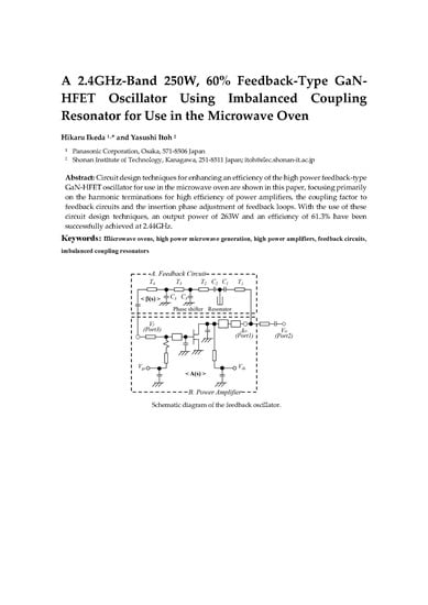
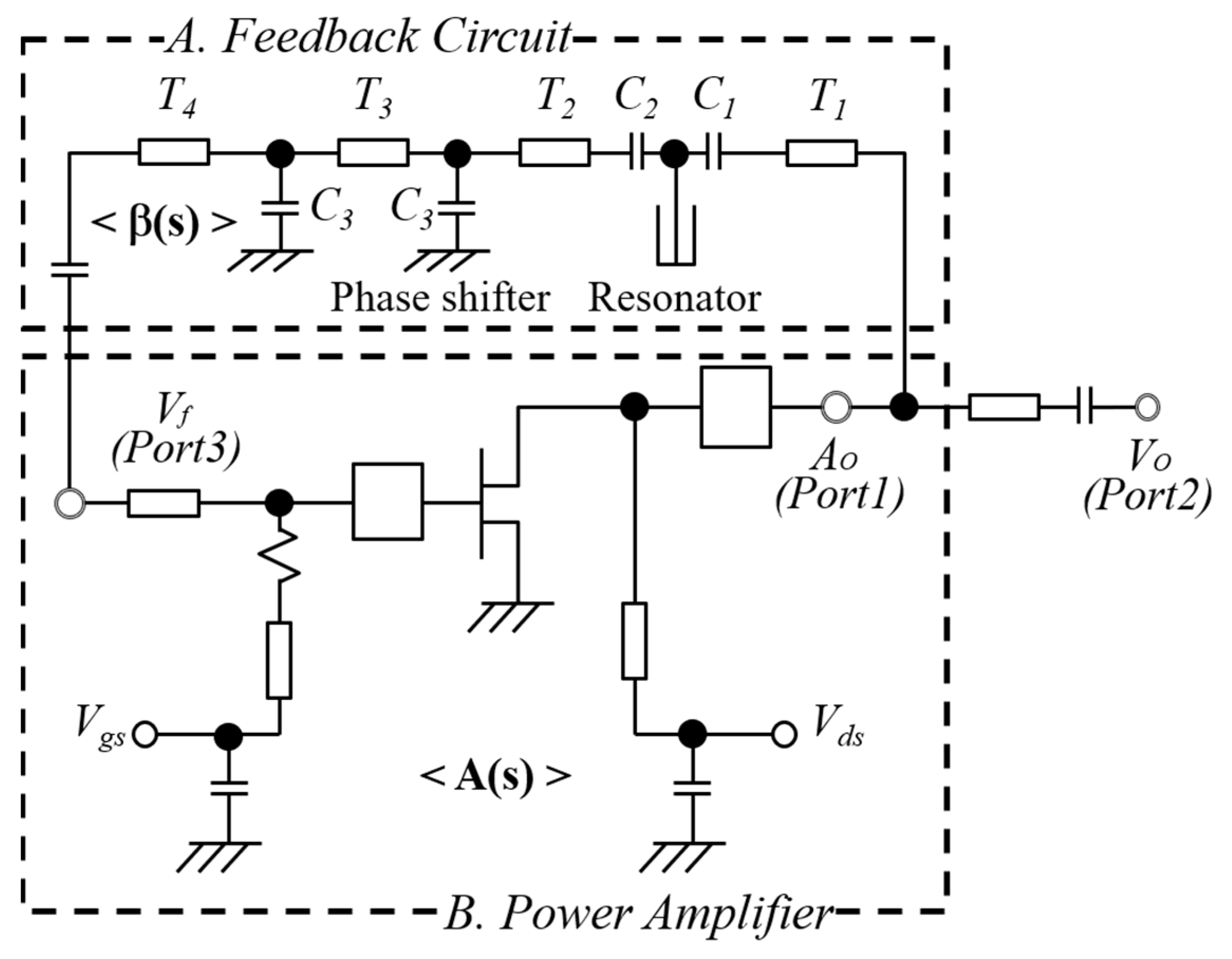
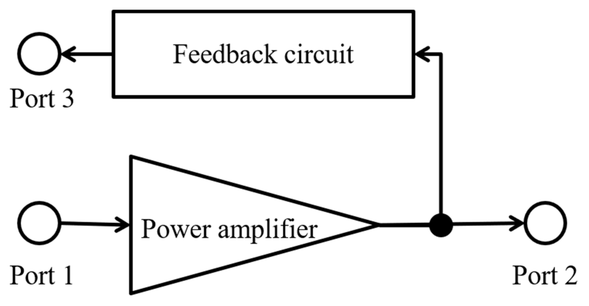
A schematic diagram of the feedback-type oscillator is shown in Figure 1. It consists of the feedback circuit (A) and the power amplifier (B). The feedback circuit (A) picks up a part of the output signal and then takes back to the input of the power amplifier (B) via the imbalanced coupling resonator and the phase shifter. The insertion characteristics of the feedback circuit and power amplifier are defined as β(s) and A(s), respectively. To achieve high efficiency of the feedback-type oscillator, it becomes crucial how to achieve high efficiency of the power amplifier by harmonic terminations in addition to making the feedback amount as small as possible. To achieve high efficiency of the power amplifier, GaN-HFETs in place of the conventional LDMOS are employed because of high gm and ft. In addition, the harmonic termination is utilized in the design of the power amplifier (B). On the other hand, the value of C1 of the imbalanced coupling capacitor has to be small to achieve a weak coupling for improving an insertion loss of the feedback circuit. On the contrary, the value of C2 has to be large to achieve a strong coupling to the power amplifier circuit for low insertion loss and high efficiency [8,9]. The oscillation conditions are based on Barkhausen Criteria [10] as follows:
A(s)∙β(s) ≥ 1
∑Φ = 2π × n (n = 1, 2, …)
Equations (1) and (2) define its criteria for amplitude and phase, respectively.
2.1. Power Amplifier
A schematic diagram of the power amplifier is shown in Figure 2. A class-F [11] condition is employed for high efficiency. The output matching circuit was terminated by short for even harmonics as well as open for odd harmonics at a drain terminal of the device. The device used in this amplifier was GaN-HFET (MACOM MAGe-102425-300S00, Lowell, MA, 01851 USA). It is necessary to terminate up to the 3rd harmonics by considering the high frequency performances. In Figure 2, a short stub Td1 was designed as a quarter-wavelength for the fundamental frequency, which becomes a half-wavelength for the 2nd harmonics. Transmission lines Td2, Td3, short stub Td4, and shunt capacitance Cd1 consists of a low-pass filter, which becomes open at the 3rd harmonics and also achieves a complete impedance matching at the fundamental frequency. Moreover, transmission lines Tg2, Tg3, short stub Tg1, and shunt capacitance Cg1 consist of a low-pass filter, which plays the same role as the output circuit.
The circuit simulation has been done for the schematic diagram of Figure 2 by using ADS (Advanced Design System) and a nonlinear model name of “EEHEMT”. A supply voltage is +50 V and Idq is 800 mA. The simulated power, efficiency and gain were plotted in Figure 3. A small-signal gain of greater than 17 dB, a P2dB of 54.4 dBm (275 W) and a drain efficiency of 62.3% have been successfully accomplished at 2.45 GHz. Moreover, the measured data using LDMOS FETs (Field Effect Transistors) [9] are newly added in Figure 3 for making clear the difference between them. A magnetron oscillator has an output power of 800 W and an efficiency of 66% [12].
2.2. Feedback Circuit
In Figure 1, Ports 1, 2, and 3 are represented as an output of the power amplifier (B), an output of the oscillator, and an output of the feedback circuit (A), respectively. The insertion loss of the feedback circuit S31 has to be better than −15 dB at 2.45 GHz by considering a small signal gain of 17 dB and P2dB (2dB gain compressed power) operation of the power amplifier. The output loss of the oscillator is represented as S21. Moreover, the center frequency of the passband of the imbalanced resonator is depicted as fo. S31, S21, and fo are calculated for the schematic diagram of Figure 1 for a variable coupling capacitance C1 of 0.02 to 0.14 pF with a constant coupling capacitance C2 of 0.3 pF. The calculated results are shown in Figure 4a. Both the feedback amount S31 and output loss S21 increase, as well as the center frequency fo, decreases with C1. As the lowest value which can satisfy the Barkhausen Criteria, C1 of 0.06 pF was chosen. S31, S21, and fo are calculated again for a variable coupling capacitance C2 of 0.15 to 0.4 pF with a constant coupling capacitance C1 of 0.06 pF. The calculated results are shown in Figure 4b. On the contrary, both the feedback amount S31 and output loss S21 decreases, as well as the center frequency fo, increases with C1. As the highest value which can satisfy the Barkhausen Criteria, C2 of 0.3 pF was chosen. In the references [8,9], only the transmission lines T1 and T2 are used to adjust the insertion phase, which seriously made a phase adjustment more difficult. To address this issue, as shown in Figure 1, the phase shifter was newly employed in the feedback circuit to adjust the insertion phase. When T3 is 14 mm and C3 is varied from 0.1 to 1.7 pF, the phase-shifter of Figure 1 can be varied by 70 degrees, allows fine adjustment of feedback loop phase. The length of T3 is shorter than λ/4 to improve the impedance of the phase shifter.
2.3. High Power Oscillator
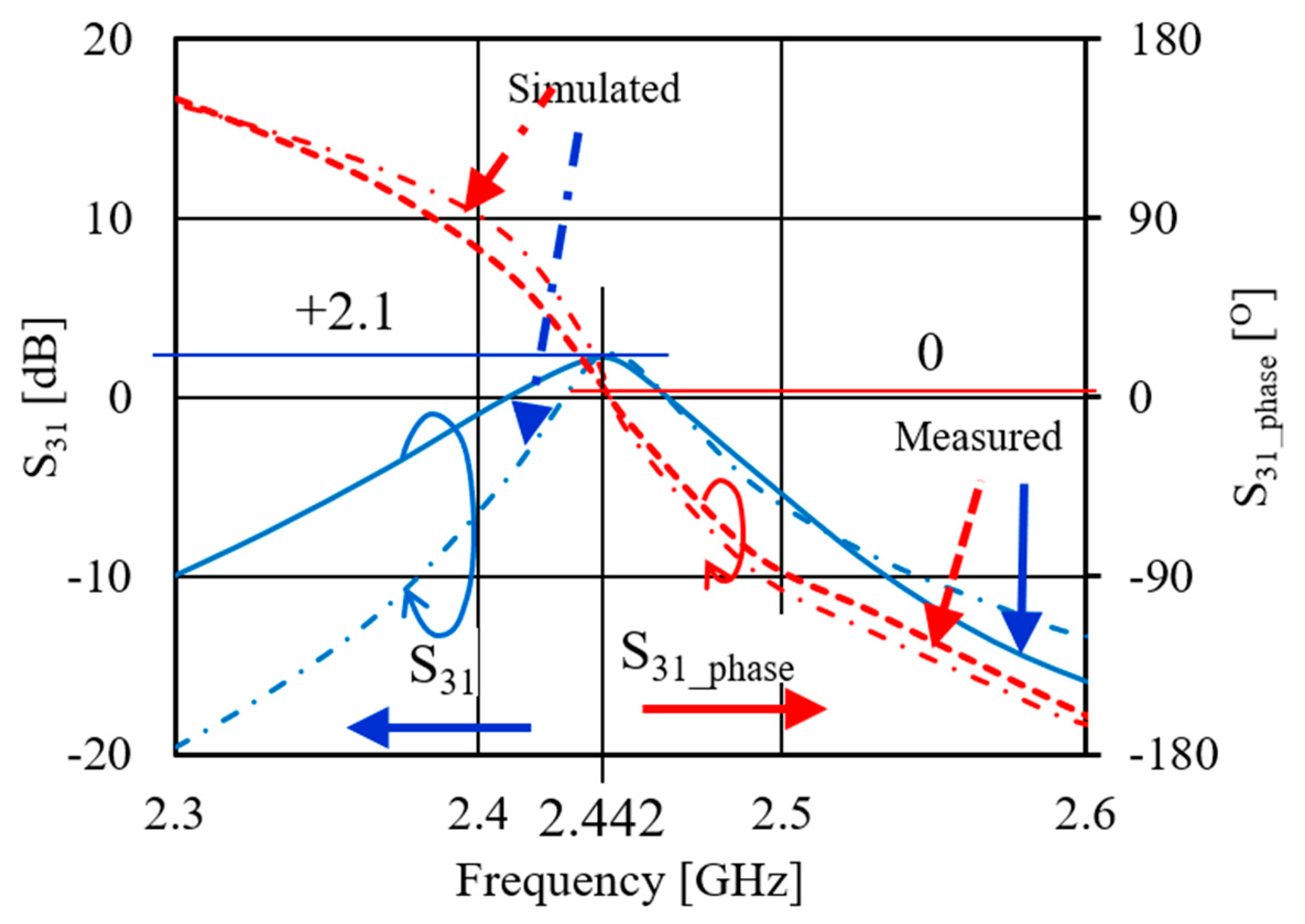
A block diagram of the high power oscillator is shown in Figure 5. Port 1, 2, and 3 are represented as an input of the power amplifier, an output of the oscillator, and an output of the feedback circuit, respectively. S31 and S21 are simulated and plotted in Figure 6. The simulated magnitude and phase of S31 are +2.4 dB and +1.7 degrees at 2.445 GHz, which meets the Equations (1) and (2).
A precise schematic diagram of the high power oscillator connecting Ports 1 and 3 is shown in Figure 7. The simulated output spectrum of the high power oscillator is shown in Figure 8. An output power of 54.2 dBm (263 W) and a drain efficiency of 61.2% has been obtained at 2.453 GHz. In comparison with Figure 3 of the power amplifier, the output power becomes smaller by 0.2 dB and efficiency of 1.1%, which greatly attributes to the insertion loss of around 0.15 dB of the feedback circuit as well as the variations of the matching condition of the power amplifier.
3. Circuit Fabrication and Results
A photograph of the high power oscillator module is shown in Figure 9. Discrete circuit elements are mounted on the Rogers substrate (4350 B) with 100 × 50 × 0.76 mm3 by soldering. The high power resonator [13] is a quarter-wavelength short-circuited coaxial-type, which employs a ceramic substrate having a dielectric constant of 38 and has a dimension of 4 × 4 × 4.35 mm3. A surface mount type of the GaN-HFET was directly die-attached to the case by soldering. The parasitic inductances and capacitances included in the circuit elements of Figure 9 have a serious effect on the performance, which are carefully taken into account the circuit simulation. The circulator was employed at the output port of the high power oscillator in order not to be affected by load impedance changes. In Figure 9, T1, T2 and T4 are transmission lines. T3 is a transmission line of the phase shifter. C1 and C2 are coupling capacitors. C3 are capacitances of the phase shifter. Vg and Vd are a gate and drain voltages, respectively. MO is an output port of a module. Water cooling was employed to dissipate heat.
Measured output power and efficiency of the power amplifier are plotted in Figure 10. A small-signal gain of 17 dB, a P2dB of 54.4 dBm (275 W) and a drain efficiency of 62.7% have been obtained at 2.45 GHz. In comparison with the simulated results of Figure 3, almost the same values have been successfully achieved. The magnitude and phase of the S31 of Figure 5 were measured and plotted in Figure 11. Mag(S31) was +2.1 dB at Ang(S31) of 0° at 2.442 GHz, which satisfies the Equations (1) and (2).
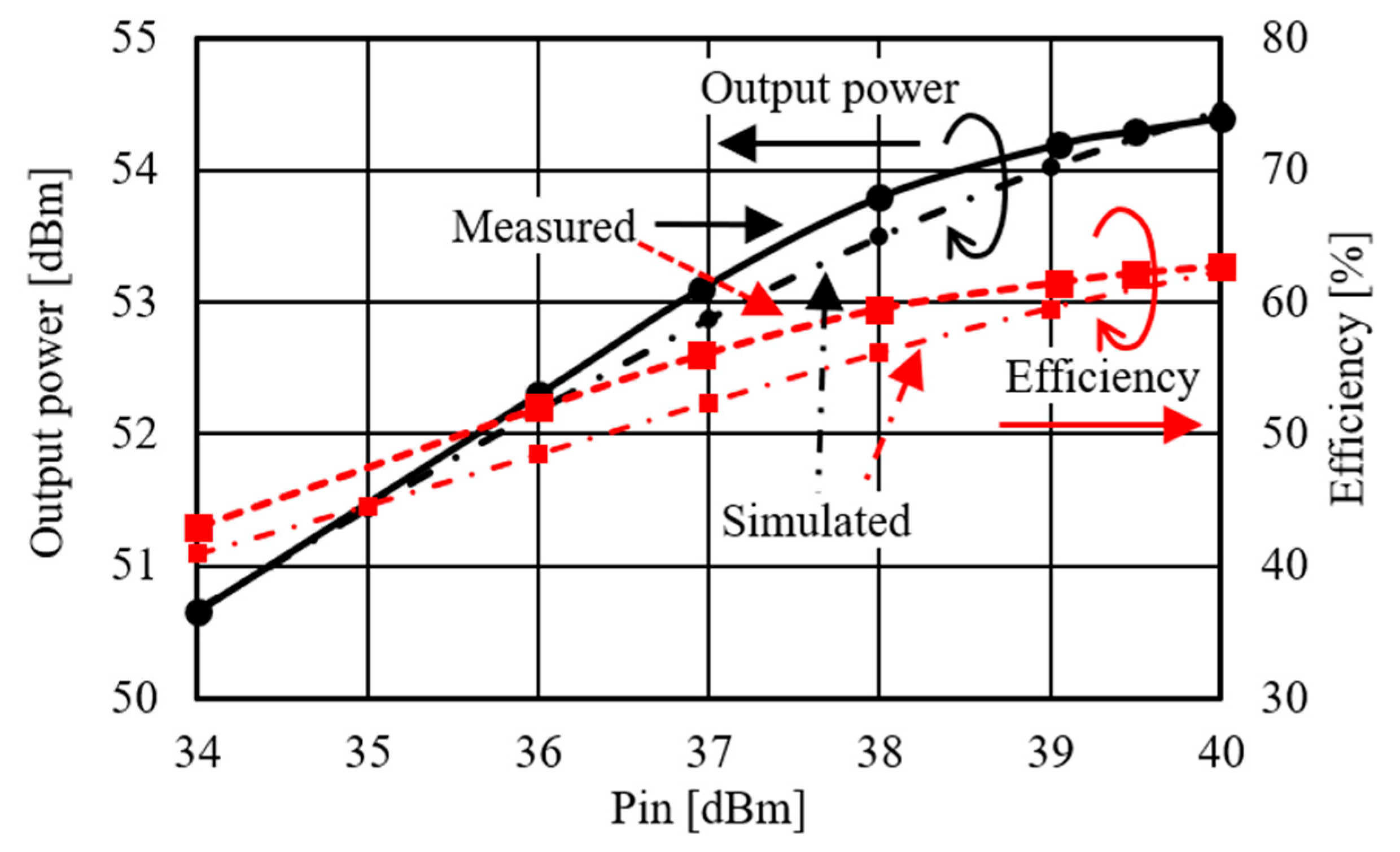
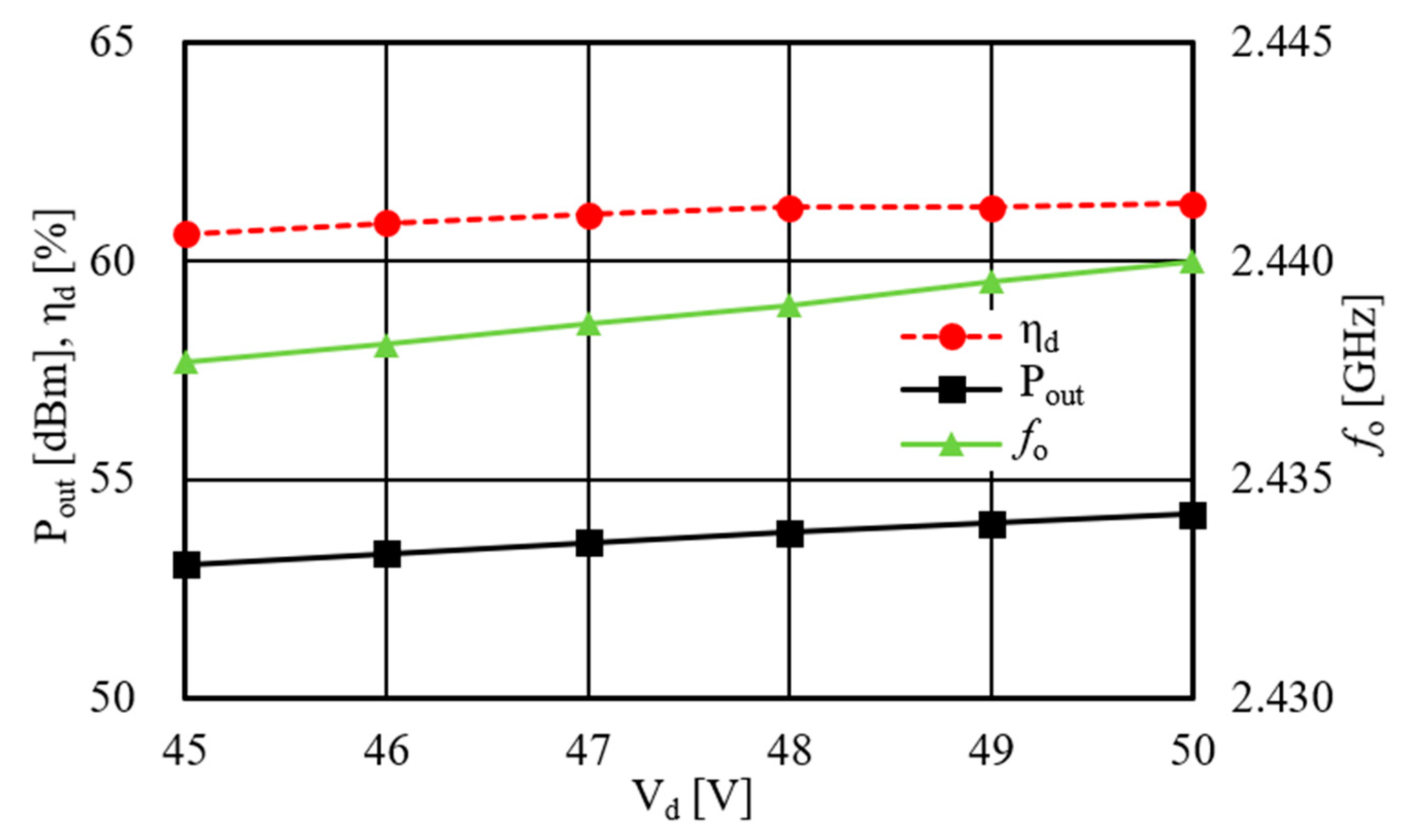
The measured output power and efficiency of the module with the circulator are plotted in Figure 12. Vd was varied from +45 to +50 V. As Vd increases, the output power, and the oscillation frequency increase. The efficiency, however, keeps around constant for Vd of +45 to +50 V. In the case with the circulator of Figure 12, an output of 54.2 dBm (263 W), an efficiency of 61.3%, and an oscillation frequency of 2.44 GHz were obtained at a supply voltage of +50 V. Now it is assumed that the insertion loss of the circulator is 0.15 dB. Then the output power and drain efficiency before the circulator become 54.4 dBm (275 W) and 63.5% at VO in Figure 9, respectively, which are in good agreement with the measured power amplifier results.
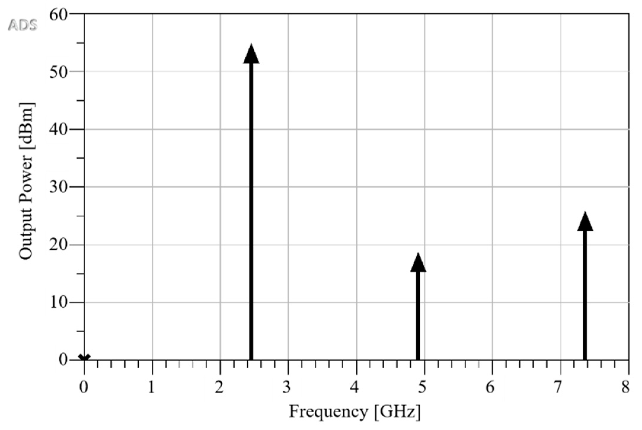
The measured output spectrum was plotted in Figure 13. The output power of 54.2 dBm (263 W) and a drain efficiency of 61.3% have been accomplished at 2.44 GHz. Vd was +50 V. The measured C/N was −100 dBc/Hz at 100 kHz offset frequency. Spurious responses appear in Figure 13. It is mainly due to the switching noise of 250 kHz for use in the generation of the negative gate voltage of Vg from the positive drain voltage of Vd. This noise was amplified and then appeared in the output spectrum of Figure 13.
A PWM (Pulse Width Modulation) becomes necessary in the actual microwave oven. The measured PWM output waveform was displayed in Figure 14, where ON/OFF time is 20 ms, respectively. We realized high speed rise and fall within 1 ms.
4. Comparative Analysis
A comparative analysis is summarized in Table 1. It is clearly shown that the efficiency can be improved by around 10% with the introduction of the imbalanced resonator in addition to around 10% with the replacement of LDMOS by GaN-HFET. In general, there exists a serious tradeoff between the output power and the efficiency. However, there is no such criteria representing this tradeoff.
5. Conclusions
The circuit design techniques for improving the efficiency of the high power feedback-type oscillator have been demonstrated in this paper: the harmonic terminations for high efficiency of power amplifiers, the coupling factor to feedback circuits, the insertion phase adjustment of feedback loops and the replacement of LDMOS with GaN-HFET. With the use of these circuit design techniques, an output power of 263 W and an efficiency of 61.3% have been successfully achieved at 2.44 GHz. The results mean that the circuit design techniques would be one candidate for realizing the next generation intelligent microwave heating using active phased array antenna modules.
Author Contributions
Conceptualization, H.I. and Y.I.; methodology, H.I. and Y.I.; software, H.I. and Y.I.; validation, H.I. and Y.Itoh; formal analysis, H.I.; investigation, H.I. and Y.I.; resources, H.I.; data curation, H.I.; writing—original draft preparation, H.I. and Y.I.; writing—review and editing, H.I. and Y.I.; visualization, H.I.; supervision, H.I.; project administration, H.I.; funding acquisition, H.I.
Funding
This research was funded by Industrial Solutions Company, Panasonic Corporation.
Conflicts of Interest
The authors declare no conflict of interest.
References
- Werner, K. RF Energy Systems: Realizing New Applications. Microwave J. 2015, 58, 22–34. [Google Scholar]
- Yakovlev, V. Computer Modeling in the Development of Mechanisms of Control over Microwave Heating in Solid-State Energy Systems. AMPERE Newsl. 2016, 89, 18–21. [Google Scholar]
- Yakovlev, V. Frequency Control over the Heating Patterns in a Solid-State Dual-Source Microwave Oven. In Proceedings of the IEEE MTT-S International Microwave Symposium, Phoenix, AZ, USA, 17–22 May 2015; pp. 1–4. [Google Scholar]
- Ikeda, H.; Kamiyama, T.; Nitta, T.; Uno, T.; Iwata, M.; Yahata, K. 1.2 kW Power Combiner Unit using Phase Control for 2.4 GHz band. In Proceedings of the IEEE International Meeting for Future of Electron Devices, Kansai (IMFEDK), Kyoto, Japan, 4–5 June 2015; pp. 1–2. [Google Scholar]
- Shi, T.; Li, K. High power solid-state oscillator for microwave oven applications. In Proceedings of the IEEE/MTT-S International Microwave Symposium Digest, Montreal, QC, Canada, 17–22 June 2012; pp. 1–4. [Google Scholar]
- Shi, T.; Li, K. High power solid-state DRO with power booster. In Proceedings of the 2012 7th European Microwave Integrated Circuit Conference, Amsterdam, The Netherlands, 29–30 October 2012; pp. 461–464. [Google Scholar]
- Kim, S.H.; Kim, H.J.; Shin, S.W.; Kim, J.D.; Kim, B.K.; Choi, J.J. Combined power oscillator using GaN HEMT. In Proceedings of the 2011 IEEE MTT-S International Microwave Symposium, Baltimore, MD, USA, 5–10 June 2011; pp. 1–4. [Google Scholar]
- Ikeda, H.; Itoh, Y. 2.4 GHz-Band High Power and High Efficiency Solid-State Injection-Locked Oscillator Using Imbalanced Coupling Resonator. In Proceedings of the 2017 IEEE MTT-S International Microwave Symposium (IMS), Honolulu, HI, USA, June 2017; pp. 1–4. [Google Scholar]
- Ikeda, H.; Itoh, Y. 2.4 GHz-band high power and high efficiency solid-state injection-locked oscillator. IEEE Trans. Microwave Theory Tech. 2018, 66, 3315–3322. [Google Scholar] [CrossRef]
- Lindberg, E. The Barkhausen criterion (observation?). In Proceedings of the IEEE Workshop Nonlinear Dynamics Electronic Systems, Dresden, Germany, 26–28 May 2010; pp. 15–18. [Google Scholar]
- Moon, J.; Jee, S.; Kim, J.; Kim, J.; Kim, B. Behaviors of class-F and class-F−1 amplifiers. IEEE Trans. Microw. Theory Tech. 2012, 60, 1937–1951. [Google Scholar] [CrossRef]
- Liu, Z.; Chen, X.; Yang, M.; Liu, C. Experimental studies on a low power injection-locked continuous wave magnetron. In Proceedings of the 2017 IEEE MTT-S International Microwave Symposium, Honolulu, HI, USA, 4–9 June 2017; pp. 1–4. [Google Scholar]
- Coaxial Resonator. Available online: http://daiken-chem.co.jp/en/q3-top/q3-seihin.html#tem (accessed on 15 July 2019).
Figure 1.
Schematic diagram of the feedback oscillator.

Figure 2.
Schematic diagram of the power amplifier.
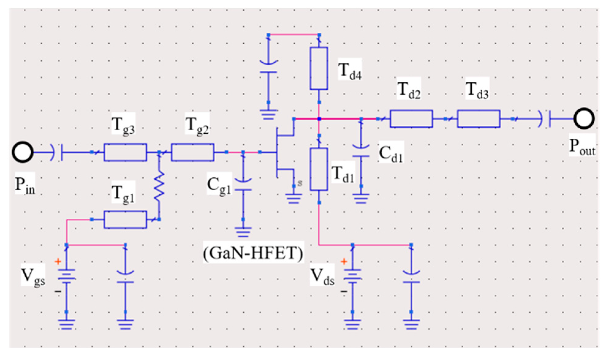
Figure 3.
Simulated power, efficiency, and gain of the power amplifier.
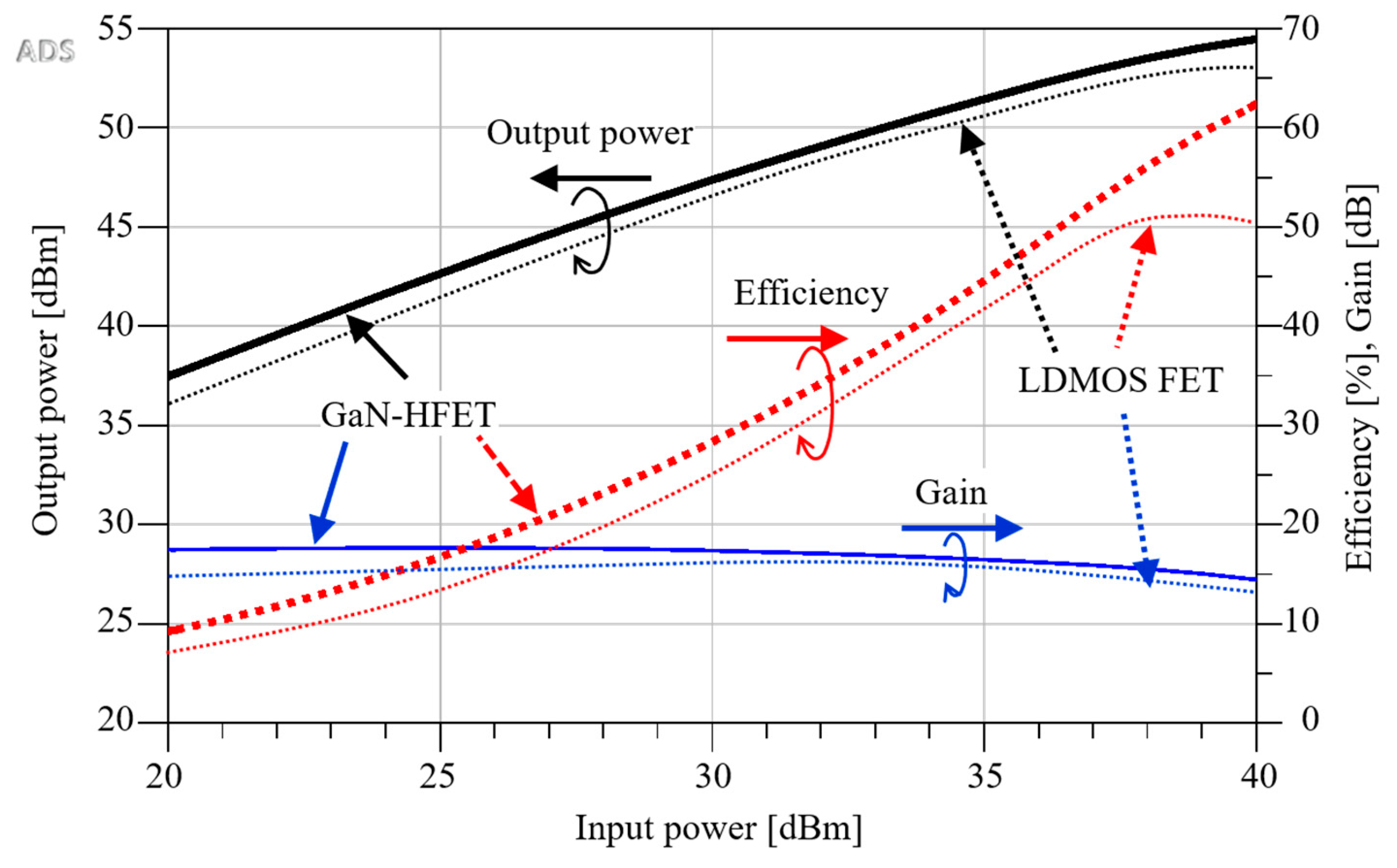
Figure 4.
Calculated S31, S21, and fo.
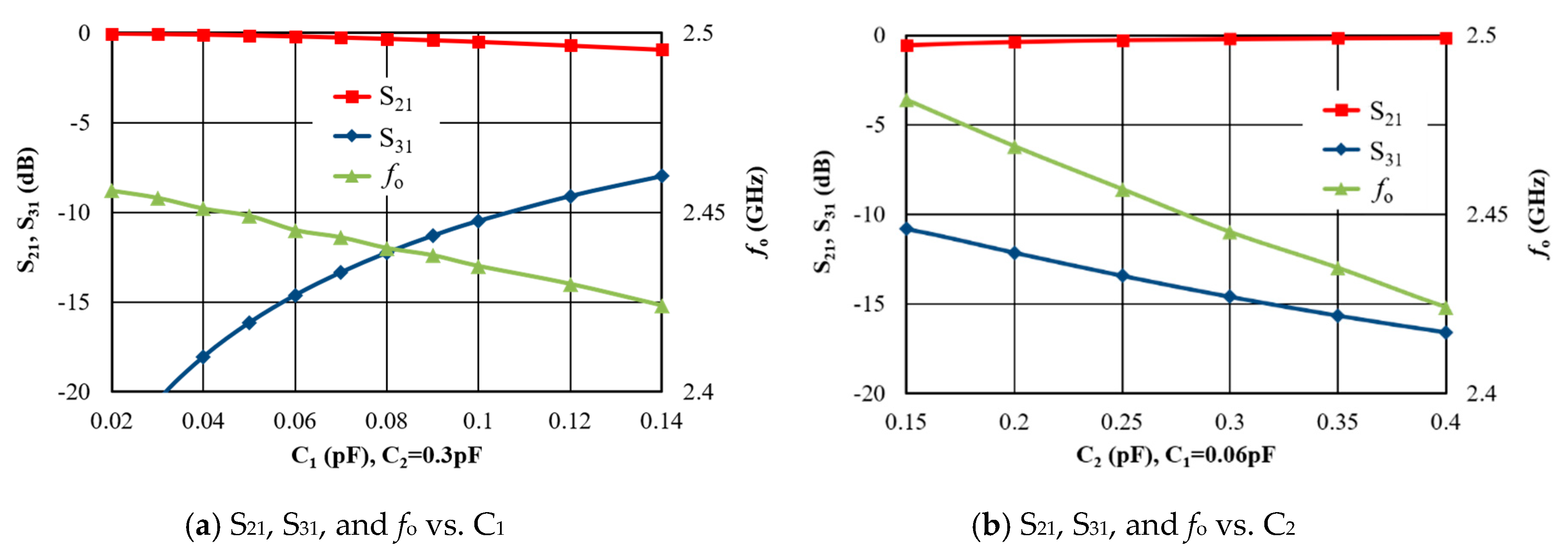
Figure 5.
Block diagram of the high power oscillator.

Figure 6.
Simulated S31 and S21 of the power oscillator.

Figure 7.
Precise schematic diagram of the high power oscillator connecting Ports 1 and 3.
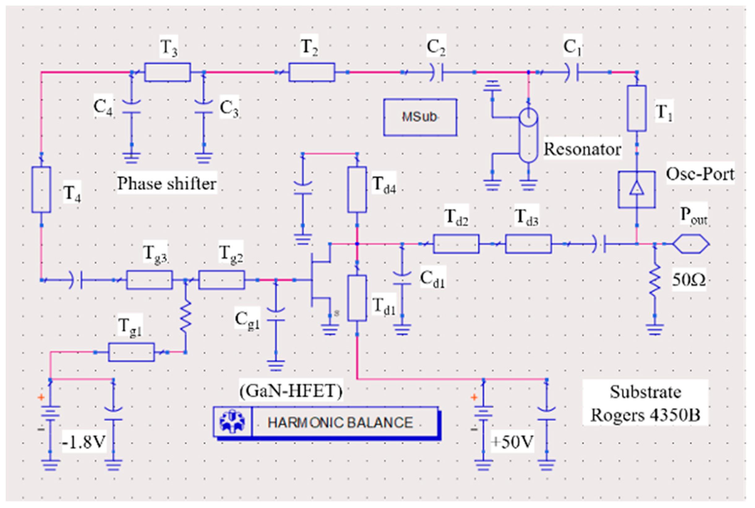
Figure 8.
Simulated output spectrum of the high-power oscillator.

Figure 9.
Photograph of the high power oscillator module.
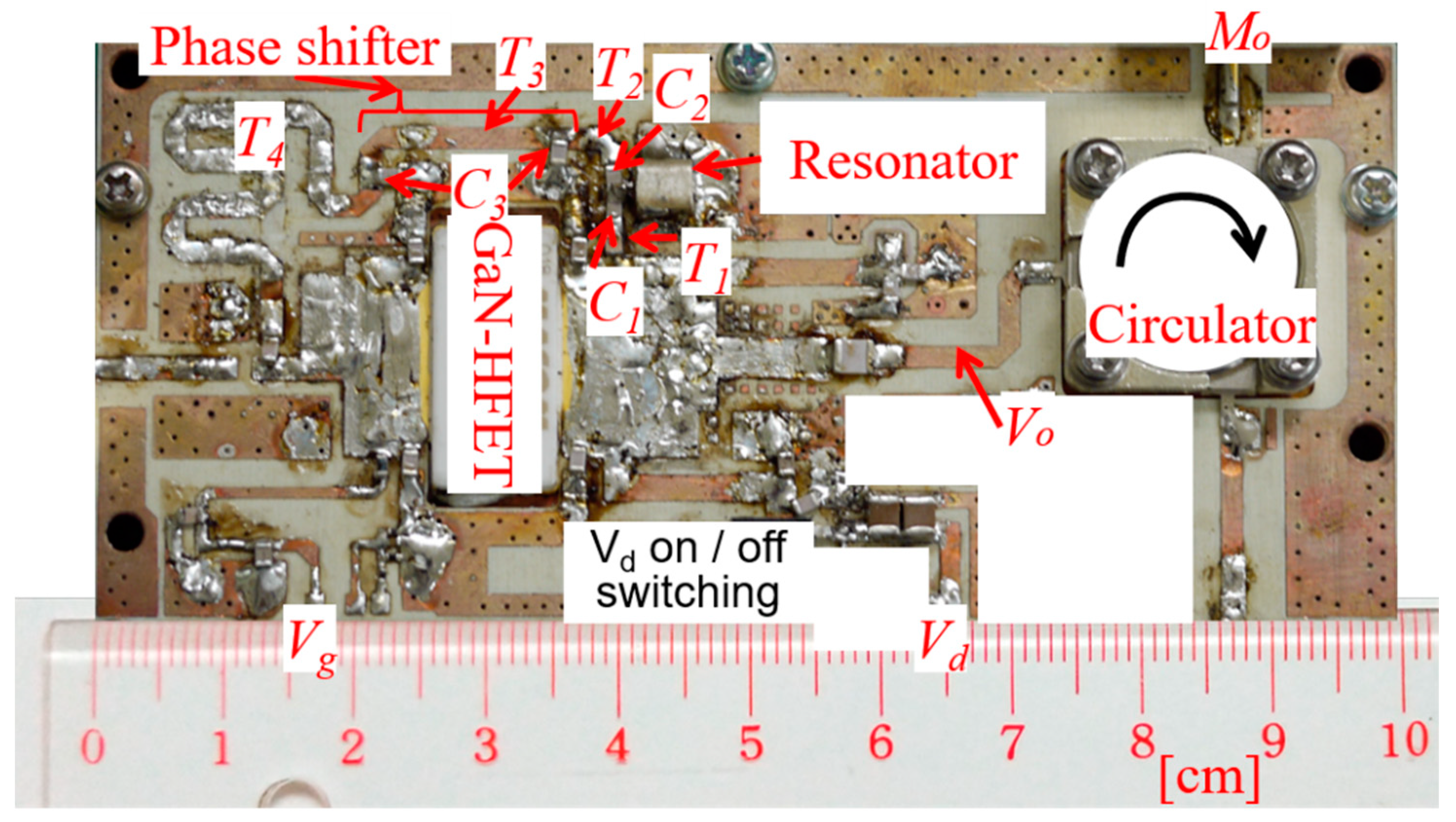
Figure 10.
Measured output power and efficiency of the power amplifier.

Figure 11.
Measured magnitude and phase of the S31 of Figure 5.
Figure 11.
Measured magnitude and phase of the S31 of Figure 5.

Figure 12.
Measured output power and efficiency of the module with the circulator.

Figure 13.
Measured output spectrum.

Figure 14.
Measured PWM output waveform.


Table 1.
Comparative analysis of the high power oscillators.
| Reference | Output Power (W) | Efficiency (%) | Device | Resonator |
|---|---|---|---|---|
| (5) | 157 (310) | 44 (46) | LDMOS | Ring |
| (6) | 138 (330) | 41 (45) | LDMOS | Dielectric |
| (7) | 48 | 58 | GaN-HEMT *1 | - |
| (9) | 210 | 51 | LDMOS | Coaxial |
| This work | 263 | 61 | GaN-HFET | Coaxial |
( ): 2 devices are used; *1 Gallium Nitride–High Electron Mobility Transistor
© 2019 by the authors. Licensee MDPI, Basel, Switzerland. This article is an open access article distributed under the terms and conditions of the Creative Commons Attribution (CC BY) license (http://creativecommons.org/licenses/by/4.0/).
Share and Cite
MDPI and ACS Style
Ikeda, H.; Itoh, Y. A 2.4 GHz-Band 250 W, 60% Feedback-Type GaN-HFET Oscillator Using Imbalanced Coupling Resonator for Use in the Microwave Oven. Appl. Sci. 2019, 9, 2887. https://doi.org/10.3390/app9142887
AMA Style
Ikeda H, Itoh Y. A 2.4 GHz-Band 250 W, 60% Feedback-Type GaN-HFET Oscillator Using Imbalanced Coupling Resonator for Use in the Microwave Oven. Applied Sciences. 2019; 9(14):2887. https://doi.org/10.3390/app9142887
Chicago/Turabian StyleIkeda, Hikaru, and Yasushi Itoh. 2019. "A 2.4 GHz-Band 250 W, 60% Feedback-Type GaN-HFET Oscillator Using Imbalanced Coupling Resonator for Use in the Microwave Oven" Applied Sciences 9, no. 14: 2887. https://doi.org/10.3390/app9142887
Note that from the first issue of 2016, this journal uses article numbers instead of page numbers. See further details here.