Silicon Meets Graphene for a New Family of Near-Infrared Schottky Photodetectors

Institute for Microelectronics and Microsystems—Italian National Council of Research, 80131 Napoli, Italy
Appl. Sci. 2019, 9(18), 3677; https://doi.org/10.3390/app9183677
Submission received: 4 July 2019
/
Revised: 23 July 2019
/
Accepted: 15 August 2019
/
Published: 5 September 2019
(This article belongs to the Special Issue Silicon Photonics – Emerging Devices and Applications)
Abstract
:In recent years, graphene has attracted much interest due to its unique properties of flexibility, strong light-matter interaction, high carrier mobility and broadband absorption. In addition, graphene can be deposited on many substrates including silicon with which is able to form Schottky junctions, opening the path to the realization of near-infrared photodetectors based on the internal photoemission effect where graphene plays the role of the metal. In this work, we review the very recent progress of the near-infrared photodetectors based on Schottky junctions involving graphene. This new family of device promises to overcome the limitations of the Schottky photodetectors based on metals showing the potentialities to compare favorably with germanium photodetectors currently employed in silicon photonics.
1. Introduction
The field of silicon photonics (Si PDs) is nowadays an emerging market promising to reach a value of more than $4 billion in the 2024 as shown in Figure 1. Indeed, both switching and interconnects of the existing data center will no longer support the huge increase in internet data traffic driven by the social network and video contents.
This is because in the near future new technologies must be introduced. The research activity in Silicon photonics can be dated back to the 1980s and in recent years more and more players are emerging in this industry’s landscape. Nowadays, Intel shares the leadership in this field with Luxtera, with products for 100 G data rates already present on the market. As Silicon (Si) is a mature technology developed during the years of the strong expansion of the microelectronic industry, the use of Si for the fabrications of photonic components meet the requirements of the data center in term of low cost, reliability, integration density and power consumption. A key component in Si photonics is constituted by the photodetectors (PDs), devices that are able to convert the incoming light into current.
Si PDs are commercial devices in the visible spectrum, however, the employment of Si for the realization of PD operating at near-infrared (NIR) wavelengths is not a simple task due to Si transparence above 1.1 μm. NIR Si PDs take conventionally advantage of germanium (Ge) integration [2,3] on Si, however, due to a 4.3% lattice mismatch, very high leakage current hinders the device performance. This issue can be mitigated by realizing a buffer layer based on a two-step epitaxial growth technique [2,3] that minimize but, unfortunately, do not remove the defect center responsible of the high leakage current. Moreover, this buffer layer generates some problems in terms of thermal budget and planarity [4] preventing the possibility of a monolithic Ge integration on Si. In addition, Ge is characterized by a low absorption at 1550 nm with respect to gallium arsenide (InGaAs) leading to thick active intrinsic region of the PIN structures and slow devices.
In this context, an all-Si approach is preferred, and one option for detecting NIR wavelengths is given by the internal photoemission effect (IPE). IPE occurs in a metal/semiconductor Schottky junction when, due to an incident optical radiation, the carriers of the metal are excited to energies above the Schottky barrier of the junction and transported in the conduction band of the semiconductor [5,6]. IPE has been widely used in high-performance platinum silicide (PtSi) and palladium silicide (Pd2Si) Schottky barrier infrared charged coupled devices (CCDs). The first generation of detectors were based on a Pd2Si/Si Schottky junctions and were developed for operating in the spectrum from 1 to 2.4 μm for satellite applications and it required an operating temperature of 120 K [7,8]. Subsequently, PtSi/Si Shottky junctions showed the capability to work at longer wavelengths, from 3 to 5 μm [9,10]. The 512 × 512 focal plane array based on PtSi requires an operating temperature of 80 K [11]. In these devices, due to the low Schottky Barrier Height (SBH), the cryogenic temperature was necessary to minimize the noise current.
In 2006, it was proposed that higher SBH should be worked with in order to use IPE at room temperature and to recover the consequently reduced efficiency by means of Fabry-Peròt resonant structures [12]. Subsequently, not only these devices were realized [13] but many other strategies were employed in order to increase the efficiency of IPE-based Si PDs at room temperature. Indeed, IPE was investigated in metallic structures at nanoscale as: Si nanoparticles (NPs) [14], stripes able to support surface plasmon polaritons (SPPs) [15,16], gratings [17] and antennas [18]. In any case, by using metal/silicon junctions, responsivities of only 5mA/W [19] and 30 mA/W [14] were reported for vertically-illuminated and waveguide PDs, respectively. This low responsivity is mainly due to the fact that the carriers that are photo-excited in the metal have a low probability to be emitted over the Schottky barrier. However, it is well-known that the carrier emission probability can be increased by reducing the metal thickness, or, in other words, that the lower the metal thickness the higher the emission probability [20,21]. This consideration leads to the idea of replacing the metals with 2D materials and, in this context, graphene is of course a good candidate. Si-based graphene PDs are typically based on field effect transistor (FET) structures and many review articles are reported about them in literature [22,23]. However, graphene PDs based on FET structures are characterized by some drawbacks: a low photo-conversion area (low efficiency) due to the fact that the internal electric field is formed only in narrow region (200 nm) close to the source and drain edges [24] and a further high dark current generated in any case when a bias drops between source and drain. On the contrary, IPE-based graphene/Si PDs promise to overcome these limitations because the photo-conversion area is linked to the graphene area in contact with Si and because the dark current is that one flowing through a reversely biased Schottky diode.
In this review article, the emerging field of the NIR IPE-based graphene/Si PDs, is presented. In the first section, IPE theory for junctions involving 2D materials will be elucidated and put in comparison with the classical theory used for metals. Then, the main structures reported in literature will be discussed and their performance will be compared. Finally, it will be highlighted as these PDs have the capabilities to compare with the Ge technology in the field of NIR detection, also offering new advantageous characteristics.
2. Theoretical Background
In order to quantify the performance of IPE-based PDs, a very important parameter is the internal quantum efficiency ηint, i.e., the ratio of the number of charge carriers generated by the PD to the number of absorbed photons. On the other hand, the external quantum efficiency ηext (the ratio of the number of charge carriers generated by the PD to the number of incident photons) is linked to the internal by ηext = A ηint, being A the active material absorption. A macroscopic magnitude is the responsivity R, i.e., the ratio of the photogenerated current (Iph) to the incident optical power (Pinc). The responsivity R is linked to the external quantum efficiency ηext by the following:
In 1931, Fowler derived the first model of carrier photoemission from metal into vacuum [25]. In the 1960s, Cohen, Vims and Archer [26] modified Fowler’s theory in order to extend the carrier photoemission into semiconductors. Subsequently, Elabd and Kosonocky reviewed the previous model and, under the zero temperature approximation, they obtained that the device internal quantum efficiency η3Dint (number of carriers generated per absorbed photons) can be written as [20]:
where the factor 1/8qΦB0 35 is very often replaced by a generic factor C (named quantum efficiency coefficient) used to put in agreement the theory with the experimental data, hν = 1242/λ0 (nm) is the photon energy being λ0 the vacuum wavelength, ΦB0 is the Schottky barrier height (SBH) under zero bias, and q is the electron charge. The 3D apex is used to indicate that the formula refers to junctions involving 3D materials, i.e., metals.
Equation (2) was derived for metal-based junctions, i.e., on three-dimensional materials, however, it has been proved that it fails to correctly describe carrier photoemission involving Schottky junctions based on two-dimensional materials [27,28], thus IPE theory must be properly modified in order to be applied to the Graphene/Si junctions whose band diagram is reported in Figure 2. It could be worth mentioning that the band structure of graphene is characterized by a valence and conduction bands touch each other at six-points in the first Brillouin zone. These particular points, where the Fermi energy is set to 0 eV, are named Dirac points. The band structure close to one of the Dirac points, responsible for the electronic properties of graphene, represents the conic surface shown in Figure 2 [29].
By following Elabd’s approach [20] the number of excited holes NT is:
where D(E) is the graphene density of states (DOS) that can be written as , [30]. E is the hole energy referred to the Fermi level, ℏ is the reduced Planck constant, vF is the Fermi velocity, and hν is the photon energy. On the other hand, the number of states N occupied by holes having a certain probability to be emitted into silicon is:
where P(E) is the carrier emission probability.
In three-dimensional materials, P(E) can be expressed as P(E) = (1 − cosϑ)/2 [20], where ϑ is the so defined carrier escape angle [20]. On the contrary, P(E) in graphene assumes a very simple value of ½ because the π orbitals are always normal to the graphene/Si interface, thus the photo-excited hole momenta can have two directions: one pointing towards Si and the other in the opposite direction [27]. Therefore, the graphene internal quantum efficiency η2Dint is [27,28]:
The 2D apex is used to indicate that the formula refers to junctions involving 2D materials, i.e., graphene.
In Figure 3 the internal quantum efficiency versus the SBH for three different wavelengths of 0.85 μm, 1.3 μm and 1.55 μm are reported in order to show that in any case the IPE effect is enhanced in junctions involving 2D materials.
3. IPE-Based Silicon Photodetectors Based on Graphene Schottky Junctions
Since its discovery in 2004, graphene has been deeply investigated [31]. Indeed, electrons move in graphene as massless particles making it suitable for fast electronics, while the wide absorption (from UV to IR) due to both intra-band and inter-band transitions [32,33] makes the material very useful in the photodetection field in particular for operation at NIR wavelengths. In 2011, Chen et al. demonstrated that graphene is able to form a Schottky junction with Si [34] and this result opened the path to the investigation of IPE in the graphene/silicon junctions for NIR detection.
NIR vertically illuminated IPE-based graphene/Si PDs were reported by Amirmazlaghani et al. in 2013 [27]. These devices are based on exfoliated graphene and show a 9.9 mA/W maximum responsivity at 1550 nm and −16 V of reverse bias applied. Indeed, as shown in Figure 4b, the difference between the photogenerated and dark current is about 51.5 nA under 5.2 μW.
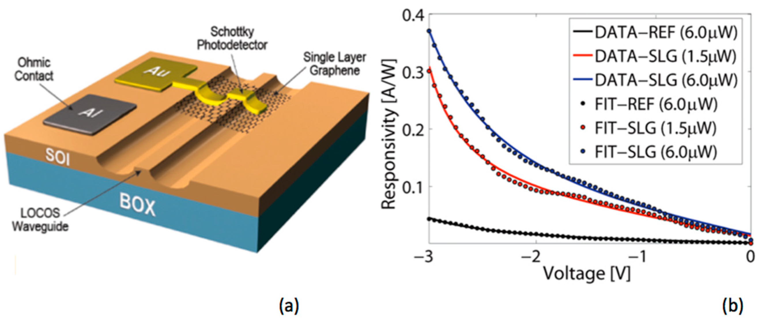
In addition, a 2.4 μA of dark current was measured while an SBH and ideality factor of 0.44–0.47 eV and 1.3–2.1 were extracted from the IV Schottky characteristic, respectively. In this paper, the authors point out the measured responsivity is much higher than that one estimated by Equation (2). This discrepancy has been explained by claiming that a new IPE theory must be derived when 2D materials are involved in the junction. Indeed, they derived a modified model (Equation (5)) for a better prediction with the experimental data. It is worth mentioning that Levy at al. have recently discussed and explained the physics behind the IPE enhancement in junctions involving 2D materials [35]. Subsequently, Goykhman et al. reported on a near-infrared graphene/Si Schottky PD integrated with a waveguide realized starting from a silicon-on-insulator (SOI) substrate. In this device the single graphene layer (SLG) is grown by chemical vapor deposition CVD system [36] (Figure 5).
The PD is constituted by a Si rib waveguide on which a SLG/Au layer acting as Schottky contact has been deposited. The collecting Ohmic contact is realized in aluminum (Al) and deposited on the Si substrate as shown on Figure 5a. The optical beam propagating along the Si waveguide is able to excite the plasmonic modes at SLG/Si interface. The photodetector length and width are ~5 μm and 310 nm, respectively. At 1 V of reverse bias applied, a responsivity at 1550 nm and dark current of 0.085 A/W and 20 nA were experimentally measured. Finally, the authors show that responsivity abruptly increases up to 0.37 A/W at −3 V. The authors explain this abrupt increase by the combined effect of two processes: avalanche multiplication within the Si depletion region and thermionic-field emission (TFE) [37] through the graphene/Si Schottky junction. Under avalanche conditions, the dark current also increases up to 3 μA. The SBH extracted by the electrical measurement is 0.34 eV.
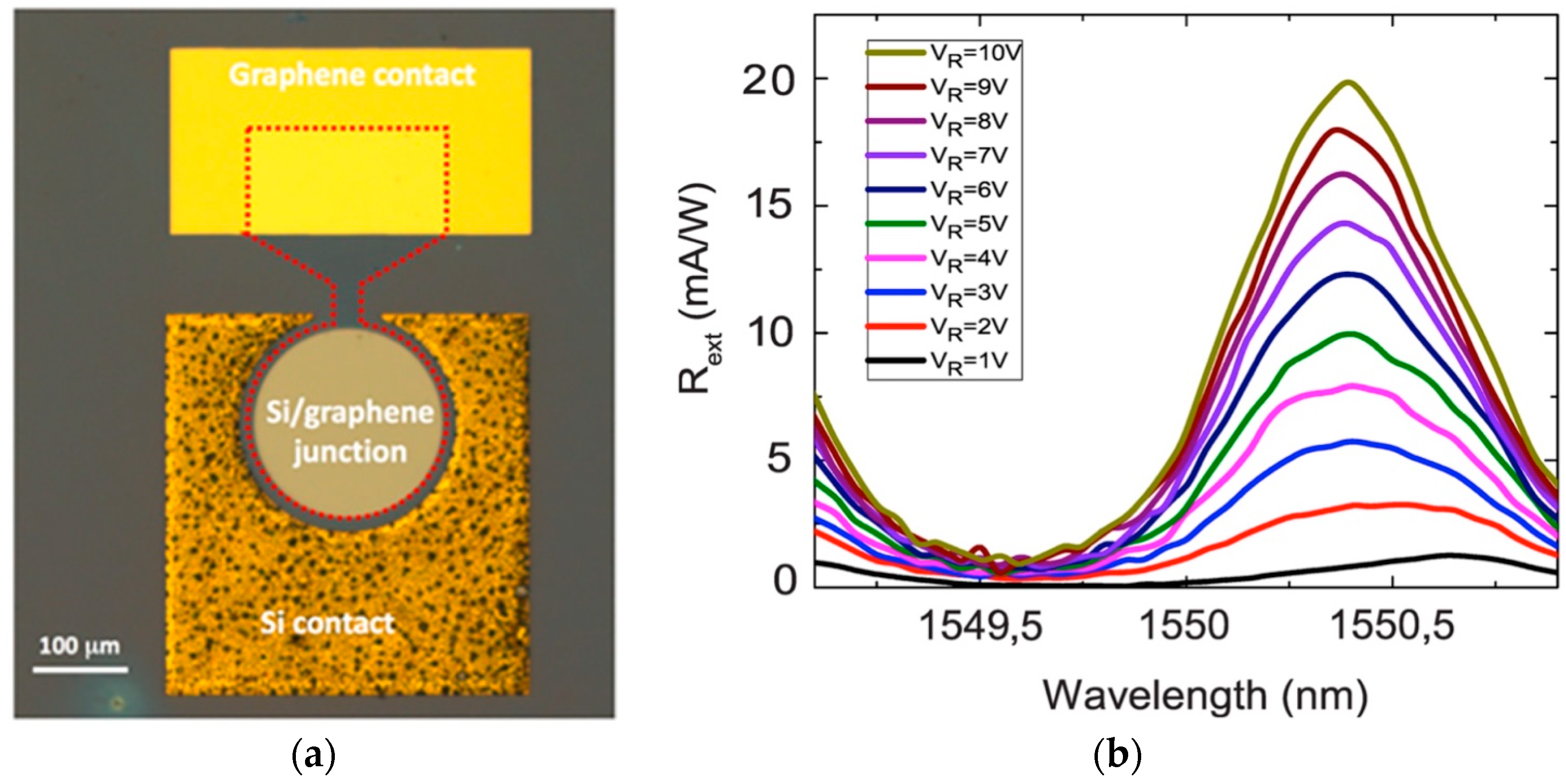
More recently, in 2017, Casalino et al. have reported on vertically-illuminated graphene/Si Schottky PDs incorporated into a Fabry-Perot optical microcavity [38]. The resonant cavity consists of a λ/2 Si slab layer surrounded between graphene/Si top and Au bottom mirrors as shown in Figure 6a. The optical cavity is able to enhance the interaction of the light with graphene in order to increase its absorption. In this work, the authors prove that the device responsivity peaks coincide with the resonances of the Fabry-Perot microcavity and that the responsivity increases with the number of light round trips of the cavity. Thanks to the multiple reflections in the cavity, the graphene absorption increases up to 8% leading to a maximum responsivity increasing with the reverse voltage applied and reaching a maximum of ~20 mA/W at −10 V (Figure 6b); this value is the highest reported so far for free-space illuminated Si PDs at 1550 nm. In addition, the authors prove the SBH dependence on applied reverse voltage. Finally, the dark current at −10 V has been measured as 147 μA while the device bandwidth has been estimated in 120 MHz.
In order to increase the low graphene absorption of the previous device (only 8%), the same author has theoretically proposed a resonant cavity-enhanced (RCE) graphene/Si PD working at 1550 nm based on IPE [39]. Device is essentially a Fabry–Perot interferometer constituted by three layers of crystalline Si, graphene and hydrogenated amorphous Si surrounded by two high-reflectivity Bragg mirrors as shown in Figure 7a. The optical field enhancement allows increasing the single-layer graphene optical absorption up to 100%. The optoelectronic transduction mechanism is based on IPE where the photoexcited carriers are emitted from graphene to Si. In this work, it has been theoretically proved that an optimized device can reach an external quantum efficiency of 35% and responsivity of 0.43 A/W, as shown in Figure 7b. Finally, device speed and noise, have been discussed.
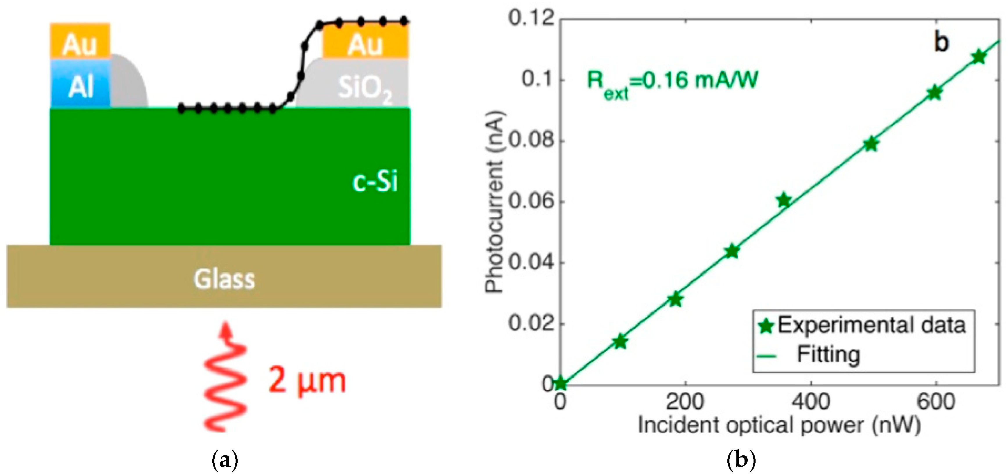
Very recently this family of devices have demonstrated the capability to work also at wavelengths longer than 1550 nm [28]. Indeed, in the Casalino’s work [28] vertically-illuminated silicon PD operating at 2 µm has been reported. The sketch of the device is shown in Figure 8a; it is a graphene/silicon Schottky junctions whose electrical parameters are carefully extracted at various temperature increasing from 280 to 315 K. The Schottky barrier is 0.62 eV at 300 K and shows a dependence on temperature ascribed to interface defects. Devices show a responsivity of 0.16 mA/W (Figure 8b) at zero bias. It corresponds to internal responsivities of at least 7.2 mA/W. Measured dark current is ~3 μA at −6 V while the estimated bandwidth is in the KHz range due to the very high series resistance. The proposed devices show the potentialities to work also at wavelength longer than 2 micron.
A summary of all the aforementioned devices are reported in Table 1 for comparison.
4. Conclusions
In this work an overview of near-infrared Si PDs based on IPE occurring in graphene, has been presented. Firstly, we have described how IPE theory needs to be properly modified in junctions involving two-dimensional material, showing as this effect is intrinsically enhanced with respect to classical device based on 3D materials (metals). Then we have described and discussed in detail the most common configurations reported in recent literature including both vertically-illuminated and waveguide structures. Finally, a quantitative comparison of selected device has been given and summarized in Table 1.
In some cases, this new family of devices shows performance that is already comparable to PDs based on Ge technology utilized in Si photonics for both telecom and datacom applications. In addition, these devices show the potentialities for working at longer wavelengths opening perspectives for new applications including optical communications, light-radars and biomedical imaging. However, the possibility to integrate 2D materials like graphene in Si technology for high-volume production remains a crucial point that needs to be properly addressed in the next future.
Funding
This research has received funding from the ATTRACT project funded by the EC under Crant Agreement 777222.
Conflicts of Interest
The author declares no conflict of interest.
References
- Yole Dèvelop. Available online: https://www.i-micronews.com/category-listing/product/silicon-photonics-2018.html (accessed on 28 June 2019).
- Koester, S.J.; Schaub, J.D.; Dehlinger, G.; Chu, J.O. Germanium-on-SOI infrared detectors for integrated photonic applications. IEEE J. Sel. Top. Quantum Electron. 2006, 12, 1489–1502. [Google Scholar] [CrossRef]
- Harame, D.L.; Koester, S.J.; Freeman, G.; Cottrel, P.; Rim, K.; Dehlinger, G.; Ahlgren, D.; Dunn, J.S.; Greenberg, D.; Joseph, A.; et al. The revolution in SiGe: Impact on device electronics. Appl. Surf. Sci. 2004, 224, 9–17. [Google Scholar] [CrossRef]
- Wang, J.; Lee, S. Ge-Photodetectors for Si-Based Optoelectronic Integration. Sensors 2011, 11, 696–718. [Google Scholar] [CrossRef] [Green Version]
- Casalino, M. Internal photoemission theory: Comments and theoretical limitations on the performance of near-infrared silicon schottky photodetectors. IEEE J. Quantum Electron. 2016, 52, 1–10. [Google Scholar] [CrossRef]
- Scales, C.; Berini, P. Thin-Film Schottky Barrier Photodetector Models. IEEE J. Quantum Electron. 2010, 46, 633–643. [Google Scholar] [CrossRef]
- Elabd, H.; Villani, T.; Kosonocky, W.F. Palladium-Silicide Schottky-Barrier IR-CCD for SWIR Applications at Intermediate Temperatures. IEEE ED Lett. 1982, 3, 89. [Google Scholar] [CrossRef]
- Elabd, H.; Villani, T.S.; Tower, J.R. High density Schottky-barrier IRCCD sensors for SWIR applications at intermediated temperature. In Proceedings of the SPIE’s Technical Symposium East, Arlington, VA, USA, 3–7 May 1982. [Google Scholar]
- Kosonocky, W.F.; Elabd, H.; Erhardt, H.G.; Shallcross, F.V.; Villani, T.; Meray, G.; Cantella, M.J.; Klein, J.; Roberts, N. 64 × 128-Elements High-Performance PtSi IR-CCD Image Sensor. In Proceedings of the 1981 International Electron Devices Meeting, Washington, DC, USA, 7–9 December 1981. [Google Scholar]
- Kosonocky, W.F.; Elabd, H.; Erhardt, H.G.; Shallcross, F.V.; Meray, G.M.; Villani, T.S.; Groppe, J.V.; Miller, R.; Frantz, V.L.; Cantella, M.J.; et al. Design and performance of 64 × 128-element PtSi Schottky-barrier IR-CCD focal plane array. In Proceedings of the SPIE’s Technical Symposium East, Arlington, VA, USA, 3–7 May 1982. [Google Scholar]
- Wang, W.-L.; Winzenread, R.; Nguyen, B.; Murrin, J.J. High fill factor 512 x 512 PtSi focal plane array. In Proceedings of the SPIE’s 33rd Annual Technical Symposium, San Diego, CA, USA, 22 December 1989. [Google Scholar]
- Casalino, M.; Sirleto, L.; Moretti, L.; Della Corte, F.; Rendina, I. Design of a silicon resonant cavity enhanced photodetector based on the internal photoemission effect at 1.55 µm. J. Opt. A Pure Appl. Opt. 2006, 8, 909–913. [Google Scholar] [CrossRef]
- Casalino, M.; Sirleto, L.; Moretti, L.; Gioffrè, M.; Coppola, G.; Rendina, I. Silicon resonant cavity enhanced photodetector based on the internal photoemission effect at 1.55 micron: Fabrication and characterization. Appl. Phys. Lett. 2008, 92, 251104. [Google Scholar] [CrossRef]
- Zhu, S.; Chu, H.S.; Lo, G.Q.; Bai, P.; Kwong, D.L. Waveguide-integrated near-infrared detector with self-assembled metal silicide nanoparticles embedded in a silicon p-n junction. Appl. Phys. Lett. 2012, 100, 61109. [Google Scholar] [CrossRef]
- Berini, P.; Olivieri, A.; Chen, C. Thin Au surface plasmon waveguide Schottky detectors on p-Si. Nanotechnology 2012, 23, 444011. [Google Scholar] [CrossRef]
- Akbari, A.; Tait, R.N.; Berini, P. Surface plasmon waveguide Schottky detector. Opt. Express 2010, 18, 8505–8514. [Google Scholar] [CrossRef] [PubMed]
- Sobhani, A.; Knight, M.W.; Wang, Y.; Zheng, B.; King, N.S.; Brown, L.V.; Fang, Z.; Nordlander, P.; Halas, N.J. Narrowband photodetection in the near-infrared with a plasmon-induced hot electron device. Nat. Commun. 2013, 4, 1643. [Google Scholar] [CrossRef] [PubMed] [Green Version]
- Knight, M.W.; Sobhani, H.; Nordlander, P.; Halas, N.J. Photodetection with active optical antennas. Science 2011, 332, 702–704. [Google Scholar] [CrossRef]
- Desiatov, B.; Goykhman, I.; Mazurski, N.; Shappir, J.; Khurgin, J.B.; Levy, U. Plasmonic enhanced silicon pyramids for internal photoemission Schottky detectors in the near-infrared regime. Optica 2015, 2, 335–338. [Google Scholar] [CrossRef] [Green Version]
- Elabd, H.; Kosonocky, W.F. Theory and measurements of photoresponse of thin film Pd2Si and PtSi Schottky-barrier detectors with optical cavity. RCA Rev. 1982, 43, 569. [Google Scholar]
- Vickers, V.E. Model of Schottky barrier hot-electron-mode photodetection. Appl. Opt. 1971, 10, 2190. [Google Scholar] [CrossRef] [PubMed]
- Wang, X.; Gan, X. Graphene integrated photodetectors and opto-electronic devices—A review. Chin. Phys. B 2017, 26, 34201. [Google Scholar] [CrossRef]
- Koppens, F.H.L.; Mueller, T.; Avouris, P.; Ferrari, A.C.; Vitiello, M.S.; Polini, M. Photodetectors based on graphene, other two-dimensional materials and hybrid systems. Nat. Nanotechnol. 2014, 9, 780–793. [Google Scholar] [CrossRef]
- Lee, E.J.; Balasubramanian, K.; Weitz, R.T.; Burghard, M.; Kern, K. Contact and edge effects in graphene devices. Nat. Nanotechnol. 2008, 3, 486–490. [Google Scholar] [CrossRef]
- Fowler, R.H. The analysis of photoelectric sensitivity curves for clean metals at various temperatures. Phys. Rev. 1931, 38, 45–56. [Google Scholar] [CrossRef]
- Cohen, J.; Vilms, J.; Archer, R.J. Investigation of Semiconductor Schottky Barriers for Optical Detection and Cathodic Emission; Report No. 68-0651; Air Force Cambridge Research Labs: Force Base, OH, USA, 1968; p. 133. [Google Scholar]
- Amirmazlaghani, M.; Raissi, F.; Habibpour, O.; Vukusic, J.; Stake, J. Graphene-Si Schottky IR detector. IEEE J. Quant. Elect. 2013, 49, 2589. [Google Scholar] [CrossRef]
- Casalino, M.; Russo, R.; Russo, C.; Ciajolo, A.; Di Gennaro, E.; Iodice, M. Free-Space Schottky Graphene/Silicon Photodetectors operating at 2 μm. ACS Photonics 2018, 5, 4577–4585. [Google Scholar] [CrossRef]
- Goncalves, P.A.D.; Peres, N.M.R. Electromagnetic properties of solids in a nutshell. In An Introduction to Graphene Plasmonics; World Scientific: Singapore, 2016; pp. 17–24. ISBN 978-981-4749-97-8. [Google Scholar]
- Van Tuan, D. Electronic and Transport Properties of Graphene. In Charge and Spin Transport in Disordered Graphene-Based Materials; Springer: Cham, Switzerland, 2016; p. 10. [Google Scholar]
- Novoselov, K.S.; Fal’ko, V.I.; Colombo, L.; Gellert, P.R.; Schwab, M.G.; Kim, K. A roadmap for graphene. Nature 2012, 490, 192–200. [Google Scholar] [CrossRef] [PubMed]
- Dawlaty, J.; Shivaraman, S.; Strait, J.; George, P.; Chandrashekhar, M.; Rana, F.; Spencer, M.G.; Veksler, D.; Chen, Y. Measurement of the optical absorption spectra of epitaxial graphene from terahertz to visible. Appl. Phys. Lett. 2008, 93, 131905. [Google Scholar] [CrossRef] [Green Version]
- Sensale-Rodriguez, B.; Yan, R.; Kelly, M.M.; Fang, T.; Tahy, K.; Hwang, W.S.; Jena, D.; Liu, L.; Xing, H.G. Efficient terahertz electro-absorption modulation employing graphene plasmonic structures. Appl. Phys. Lett. 2012, 101, 261115. [Google Scholar] [CrossRef] [Green Version]
- Chen, C.-C.; Aykol, M.; Chang, C.-C.; Levi, A.F.J.; Cronin, S.B. Graphene-silicon Schottky diodes. Nano Lett. 2011, 11, 1863–1867. [Google Scholar] [CrossRef] [PubMed]
- Levy, U.; Grajower, M.; Goncalves, P.A.D.; Mortensen, N.A.; Khurgin, J.B. Plasmonic silicon Schottky photodetectors: The physics behind graphene enhanced internal photoemission. APL Photonics 2017, 2, 26103. [Google Scholar] [CrossRef] [Green Version]
- Goykhman, I.; Sassi, U.; Desiatov, B.; Mazurski, N.; Milana, S.; De Fazio, D.; Eiden, A.; Khurgin, J.; Shappir, J.; Levy, U.; et al. On-Chip Integrated, Silicon–Graphene Plasmonic Schottky Photodetector with High Responsivity and Avalanche Photogain. Nano Lett. 2016, 16, 3005–3013. [Google Scholar] [CrossRef]
- Padovani, F.A.; Stratton, R. Field and thermionic-field emission in Schottky barriers. Solid State Electron. 1966, 9, 695–707. [Google Scholar] [CrossRef]
- Casalino, M.; Sassi, U.; Goykhman, I.; Eiden, A.; Lidorikis, E.; Milana, S.; De Fazio, D.; Tomarchio, F.; Iodice, M.; Coppola, G.; et al. Vertically Illuminated, Resonant Cavity Enhanced, Graphene-Silicon Schottky Photodetectors. ACS Nano 2017, 11, 10955–10963. [Google Scholar] [CrossRef]
- Casalino, M. Design of Resonant Cavity-Enhanced Schottky Graphene/Silicon Photodetectors at 1550 nm. J. Ligthwave Technol. 2018, 36, 1766–1774. [Google Scholar] [CrossRef]
Figure 1.
Silicon photonics 2013–2025 market forecast [1]. Reproduced with permission from S. Leroy, Director, Public Relations at Yole Développement.
Figure 1.
Silicon photonics 2013–2025 market forecast [1]. Reproduced with permission from S. Leroy, Director, Public Relations at Yole Développement.
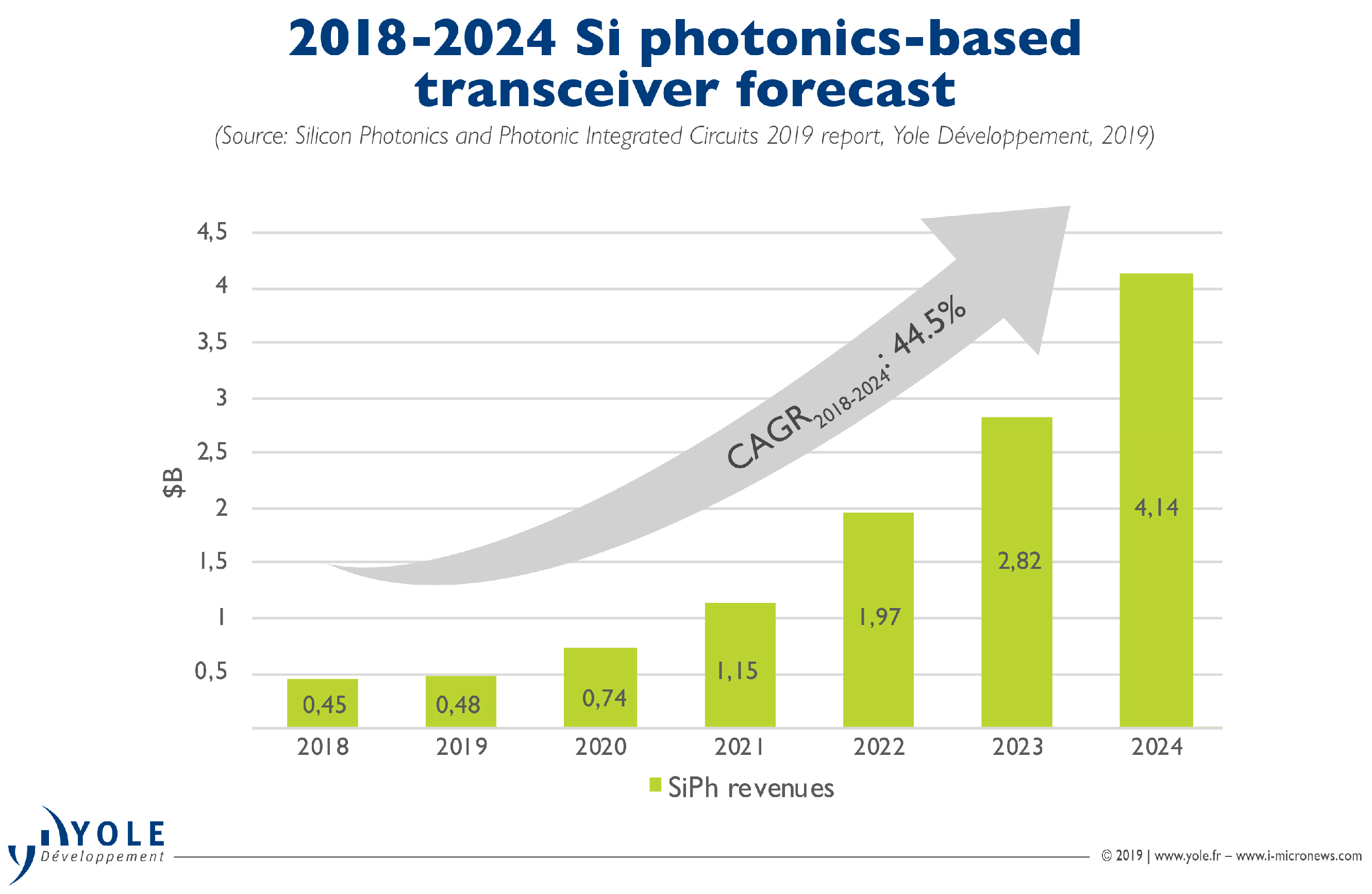
Figure 2.
Band diagram of a graphene/silicon Schottky junction: EF is the metal Fermi level, EV (EC) is the silicon valence (conduction) band, qΦB is the Schottky barrier and qVbi is the built-in potential. NT and N are the total number of states of excited holes and hole having a certain probability to be emitted into silicon.
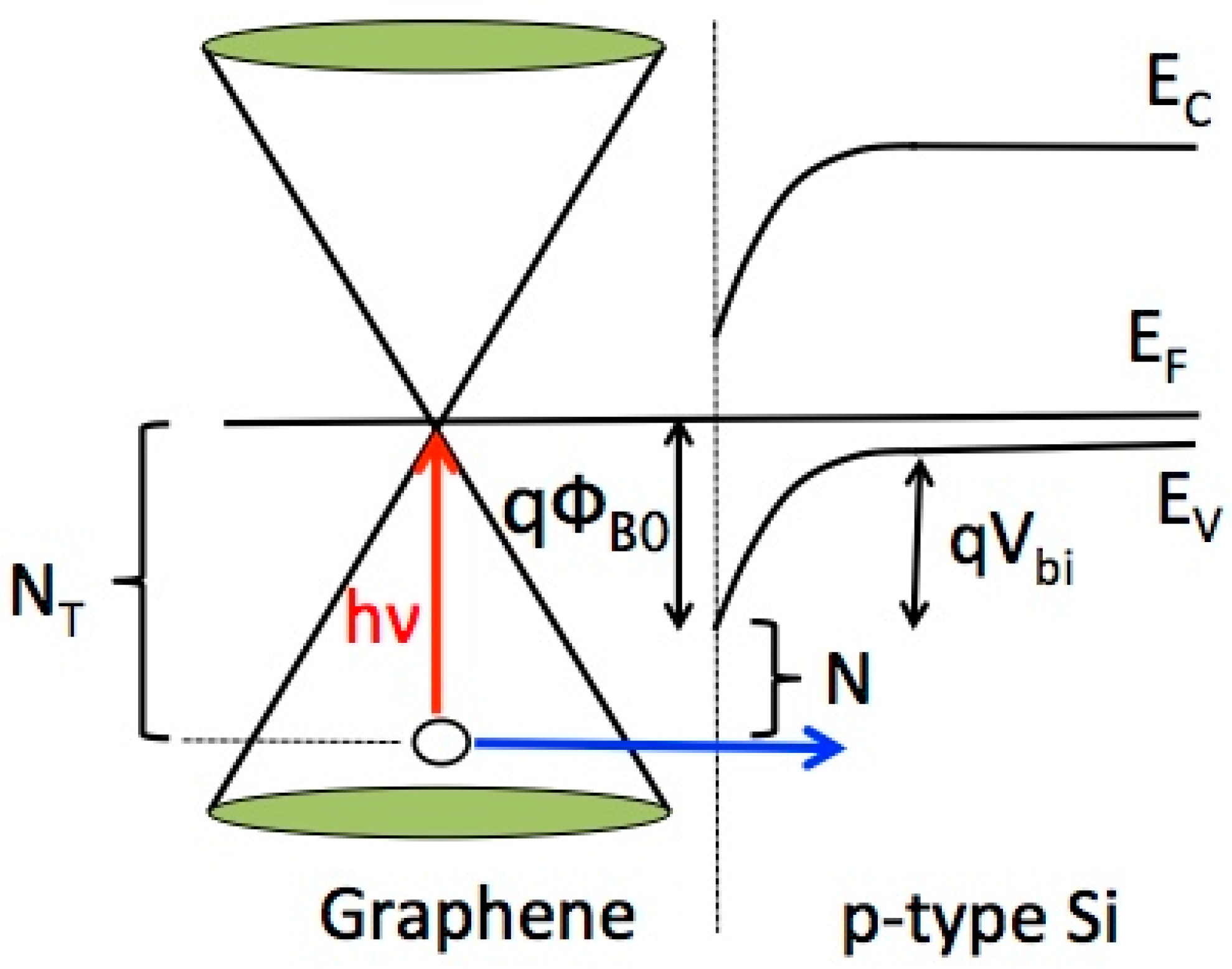
Figure 3.
Comparison between internal quantum efficiency of 3D, Equation (2), and 2D, Equation (5), materials for three different wavelengths of 0.85, 1.3 and 1.55 μm.
Figure 3.
Comparison between internal quantum efficiency of 3D, Equation (2), and 2D, Equation (5), materials for three different wavelengths of 0.85, 1.3 and 1.55 μm.
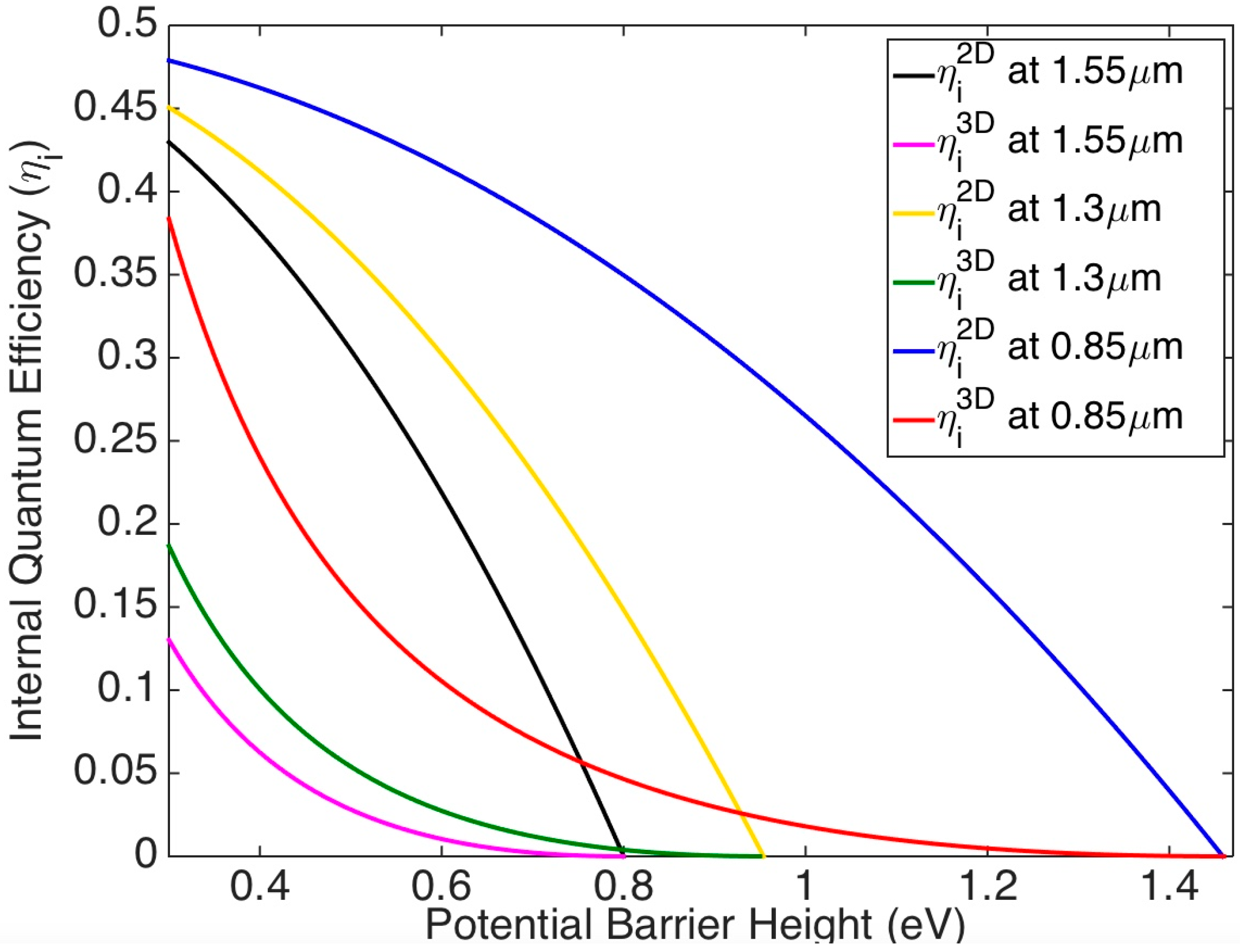
Figure 4.
(a) Sketch describing the graphene-silicon (Si) Schottky diode investigated in Amirmazlaghani [27]. (b) The current-voltage I-V curve at reverse bias (from −16 to −15 V). This figure demonstrates the change in diode current by switching on and off the laser at 1550 nm. Reprinted with permission from (Amirmazlaghani, Raissi, Habibpour, Vukusic, Stake. Graphene-Si Schottky IR detector. IEEE J. Quant. Elect. 2013, 49, 2589). Copyright (2013) IEEE.
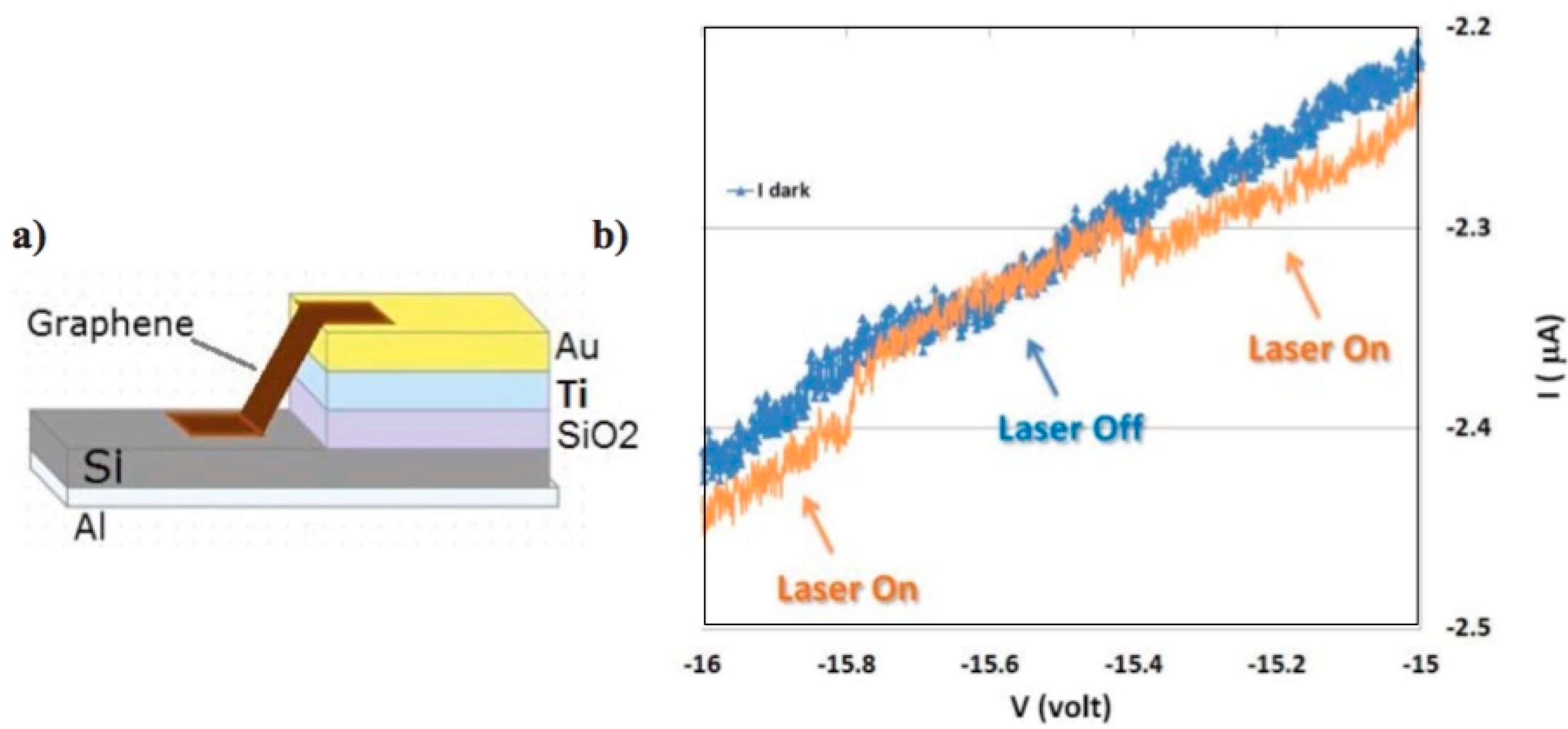
Figure 5.
(a) Scketch of the Graphene/Si Schottky photodetectors (PD) investigated in Goykhman [36]. (b) Responsivity of Graphene/Si Schottky PDs and Metal−Si PDs (for comparison). Solid lines are the curve fitting obtained by taking into account a combined avalanche multiplication and thermo field emission effect. Reprinted with permission from (Goykhman, Sassi, Desiatov, Mazurski, Milana, de Fazio, Eiden, Khurgin, Shappir, Levy, Ferrari. Integrated, Silicon–Graphene Plasmonic Schottky Photodetector with High Responsivity and Avalanche Photogain. Nano Lett. 2016, 16, 3005–3013. Direct link: https://pubs.acs.org/doi/10.1021/acs.nanolett.5b05216). Copyright (2016) American Chemical Society. Further permissions related to the material excerpted should be directed to the ACS.

Figure 6.
(a) Optical image of fabricated device investigated in Casalino [38]. (b) Responsivity vs reverse voltage. Reprinted with permission from (Casalino, Sassi, Goykhman, Eiden, Lidorikis, Milana, De Fazio, Tomarchio, Iodice, Coppola et al. Vertically Illuminated, Resonant Cavity Enhanced, Graphene-Silicon Schottky Photodetectors. ACS Nano 2017, 11, 10955–10963). Copyright (2017) American Chemical Society.

Figure 7.
(a) Section sketch and (b) theoretical responsivity and quantum efficiency of the high-finesse resonant cavity enhanced PD investigated in Casalino [39]. Reprinted with permission from (Casalino. Design of Resonant Cavity-Enhanced Schottky Graphene/Silicon Photodetectors at 1550 nm. J. Ligthwave Technol. 2018, 36, 1766–1774). Copyright (2018) IEEE.
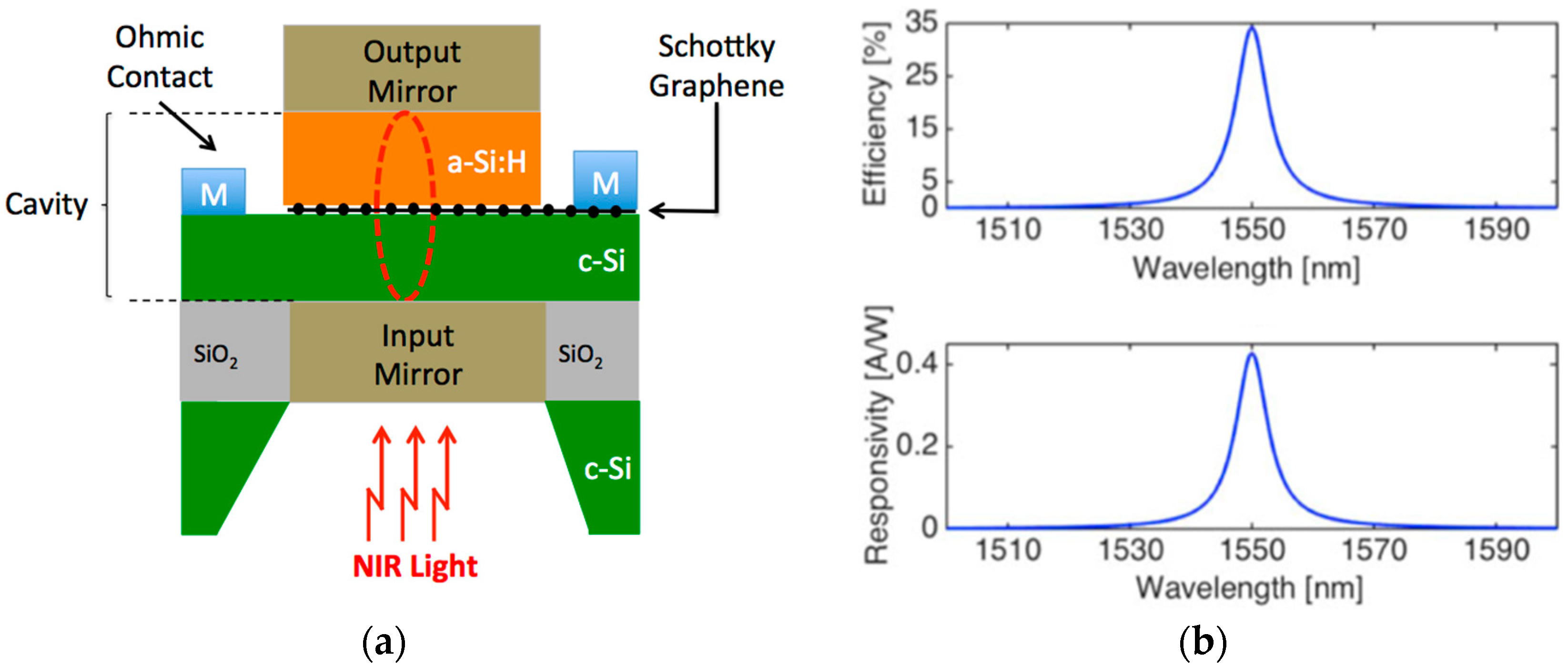
Figure 8.
(a) Schematic cross-sectional view of the graphene/Si Schottky PD investigated in Casalino [28], (b) Measured current vs incident optical radiation. Reprinted with permission from (Casalino, Russo, Russo, Ciajolo, Di Gennaro, Iodice, Coppola. Free-Space Schottky Graphene/Silicon Photodetectors operating at 2 μm. ACS Photonics 2018, 5, 4577–4585. Copyright (2018) American Chemical Society.

Table 1.
Summary of selected near-infrared silicon Schottky photodetectors based on graphene.
| Ref. | Responsivity | Dark Current | Bandwidth | SBH (eV) | Type | Conf. |
|---|---|---|---|---|---|---|
| [27] | 9.9 mA/W at 1550 nm and −16 V | ~2.4 μA at −16 V | - | 0.44–0.46 | Exfol | Free-space |
| [36] | 370 mA/W at 1550 nm and −3 V | ~3 μA at −3 V | - | 0.34 | CVD | Waveguide |
| [38] | 20 mA/W at 1550 nm and −10 V | ~147 at μA at −10 V | 120 MHz (Estimated) | 0.46 | CVD | Free-space |
| [39] * | 0.43 A/W at 1550 nm and 0 V | 561 nA if graphene radius (gr) <15 μm | GHz regime (gr <15 μm) | 0.45 | - | Free-space |
| [28] | 0.16 mA/W at 2000 nm and 0 V | ~3 μA at −6 V | KHz regime (Estimated) | 0.62 | CVD | Free-space |
* Theoretical work.
© 2019 by the author. Licensee MDPI, Basel, Switzerland. This article is an open access article distributed under the terms and conditions of the Creative Commons Attribution (CC BY) license (http://creativecommons.org/licenses/by/4.0/).
Share and Cite
MDPI and ACS Style
Casalino, M. Silicon Meets Graphene for a New Family of Near-Infrared Schottky Photodetectors. Appl. Sci. 2019, 9, 3677. https://doi.org/10.3390/app9183677
AMA Style
Casalino M. Silicon Meets Graphene for a New Family of Near-Infrared Schottky Photodetectors. Applied Sciences. 2019; 9(18):3677. https://doi.org/10.3390/app9183677
Chicago/Turabian StyleCasalino, Maurizio. 2019. "Silicon Meets Graphene for a New Family of Near-Infrared Schottky Photodetectors" Applied Sciences 9, no. 18: 3677. https://doi.org/10.3390/app9183677
Note that from the first issue of 2016, this journal uses article numbers instead of page numbers. See further details here.