Article

2D Dielectric Nanoimprinted PMMA Pillars on Metallo-Dielectric Films

by
Tiziana Stomeo
1,*,
Armando Casolino
2,
Francesco Guido
1,
Antonio Qualtieri
1,
Michael Scalora
3,
Antonella D’Orazio
2,
Massimo De Vittorio
1,4 and
Marco Grande
2,*
1
Center for Bio-Molecular Nanotechnology, Istituto Italiano di Tecnologia (IIT), Via Barsanti, 73010 Lecce, Italy
2
Dipartimento di Ingegneria Elettrica e dell’Informazione, Politecnico di Bari, Via Orabona 4, 70125 Bari, Italy
3
Charles M. Bowden Research Center, RDECOM, Redstone Arsenal, Huntsville, AL 35898-5000, USA
4
Dipartimento di Ingegneria dell’Innovazione, Università del Salento, Via Arnesano, 73100 Lecce, Italy
*
Authors to whom correspondence should be addressed.
Appl. Sci. 2019, 9(18), 3812; https://doi.org/10.3390/app9183812
Submission received: 31 July 2019 / Revised: 5 September 2019 / Accepted: 7 September 2019 / Published: 11 September 2019
(This article belongs to the Special Issue Advances on Dielectric Photonic Devices and Systems beyond Visible)

Abstract

:
In this work, we propose an optimized nanoimprint protocol for the fabrication of a two-dimensional (2D) array of polymethyl-methacrylate (PMMA) nano-pillars deposited on different sputtered configurations (bilayer and multi-layer) of copper (Cu) and aluminum nitride (AlN) slabs supported by a silicon dioxide (SiO2) substrate. Both the Cu/AlN bilayer and multilayer thin films were deposited by a sputtering technique. The sub-micron PMMA pillars were realized by using nanoimprint lithography (NIL). In order to optimize the NIL process, several tests were performed by varying temperature and pressure, allowing us to achieve uniform and high-resolution pillars. The fabricated periodic array enabled the phase-matching of the incident plane wave exciting optical resonances. All the fabricated devices were then optically characterized by means of an ad hoc setup, where the reflected light from the sample was analyzed. The fabricated nano-pillars are mechanically stable, and they could be fully exploited for the realization of novel metallo-dielectric core/shell structures for sensing, surface-enhanced Raman spectroscopy, and light–matter interactions.

1. Introduction

The optical properties of diffraction gratings have attracted great interest for a wide plethora of applications across the electromagnetic spectrum spanning from photodetectors, THz spectroscopy, optical filters, photovoltaics, and color coatings [1]. One important class of optical resonators is based on guided-mode resonances (GMRs), where a grating is exploited to excite leaky modes in a guiding layer achieving absorption on a narrowband [2]. Several examples have been proposed in the literature showing metamaterials [3,4,5,6], also combined with two-dimensional materials, such as graphene [7,8,9,10,11]. Some of these schemes use mirrors in order to obtain near-perfect absorption leading to a one-port device. Generally speaking, all these resonant structures are very sensitive to the geometrical parameters of the fabricated nanostructures, such as the sidewall of the features, and, thus, precise fabrication is indispensable to achieve the designed performance. This is critical when narrowband absorbers are considered. Consequently, the fabrication of high-quality optical gratings requires precise control of the geometrical parameters at the nanometer scale. In our previous works reported in Ref. [9,10], we have shown the excitation of GMRs in dielectric gratings, based on polymethyl-methacrylate (PMMA) strips on Ta2O5 slabs, that were realized by means of an electron-beam lithography system and were based on 1D periodic structures.
In this paper, we propose an optimized nanoimprint lithography (NIL) protocol for the fabrication of a two-dimensional (2D) array of polymethyl-methacrylate (PMMA) nano-pillars deposited on different sputtered configurations (bilayer and multi-layer) of copper (Cu) and aluminum nitride (AlN) slabs supported by a silicon dioxide (SiO2) substrate. Both the Cu/AlN bilayer and multilayer thin films were deposited by a sputtering technique, while the 2D sub-micron PMMA pillars were realized by nanoimprint lithography. The NIL technique has attracted great attention as an alternative nanopatterning technology and has found applications in many areas of nanoscale device fabrication ranging from more standard semiconductor devices [12,13] to more unique applications in optics [14,15] and plasmonics [16,17,18]. Ou et al. [19] have demonstrated that using NIL with a high aspect ratio mold, it is possible to directly imprint flexible polymer pillars that can come into nanometer proximity at a predefined symmetry, thus, opening a new path for the design and fabrication of arbitrary geometries of plasmonic nanostructures. The precise and repeatable replication of nanoscale patterns [20] from a single high-resolution patterning step makes the NIL technique much more versatile than other expensive techniques such as electron beam or even helium ion beam lithography. Compared to other lithography techniques, NIL has the advantages of being high-throughput and low-cost.
In particular, we report on the integration of NIL-based cylindrical pillars with a metallo-dielectric stack focusing on the optical behavior of the imprinted dielectric nanostructures. The fabrication parameters were studied and optimized. In order to verify the resonance behavior of the grating, we compare the performance of a bilayer (dielectric/metal or single-pair) configuration that supports GMRs with respect to a counterpart configuration where the dielectric slab is substituted by a multi-layer structure. We also investigated both configurations when a sputtered thin gold layer, introduced to avoid the charging effects during the scanning electron microscope (SEM) inspections, covers the dielectric pillar.
These fabricated structures pave the way for the realization of robust photonic devices and robust/stable hybrid structures that can efficiently combine both photonic and plasmonic resonances, taking advantage of both peculiarities [21,22].

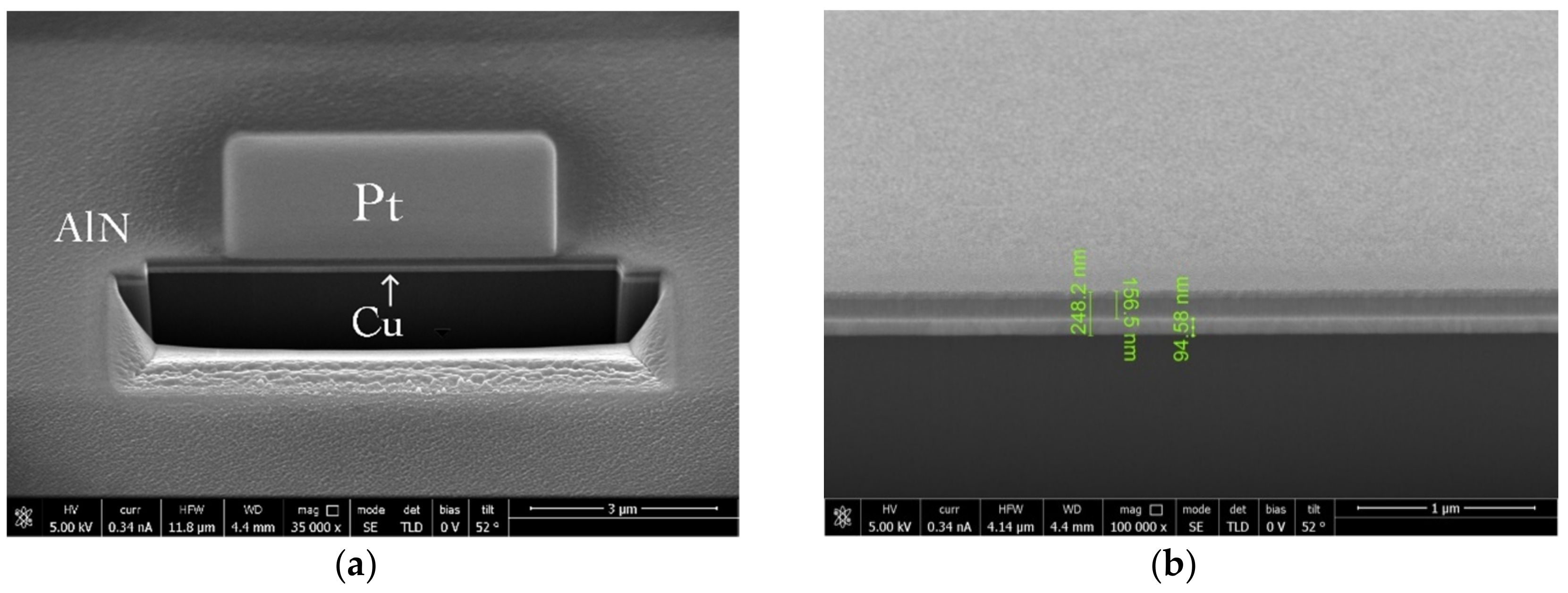
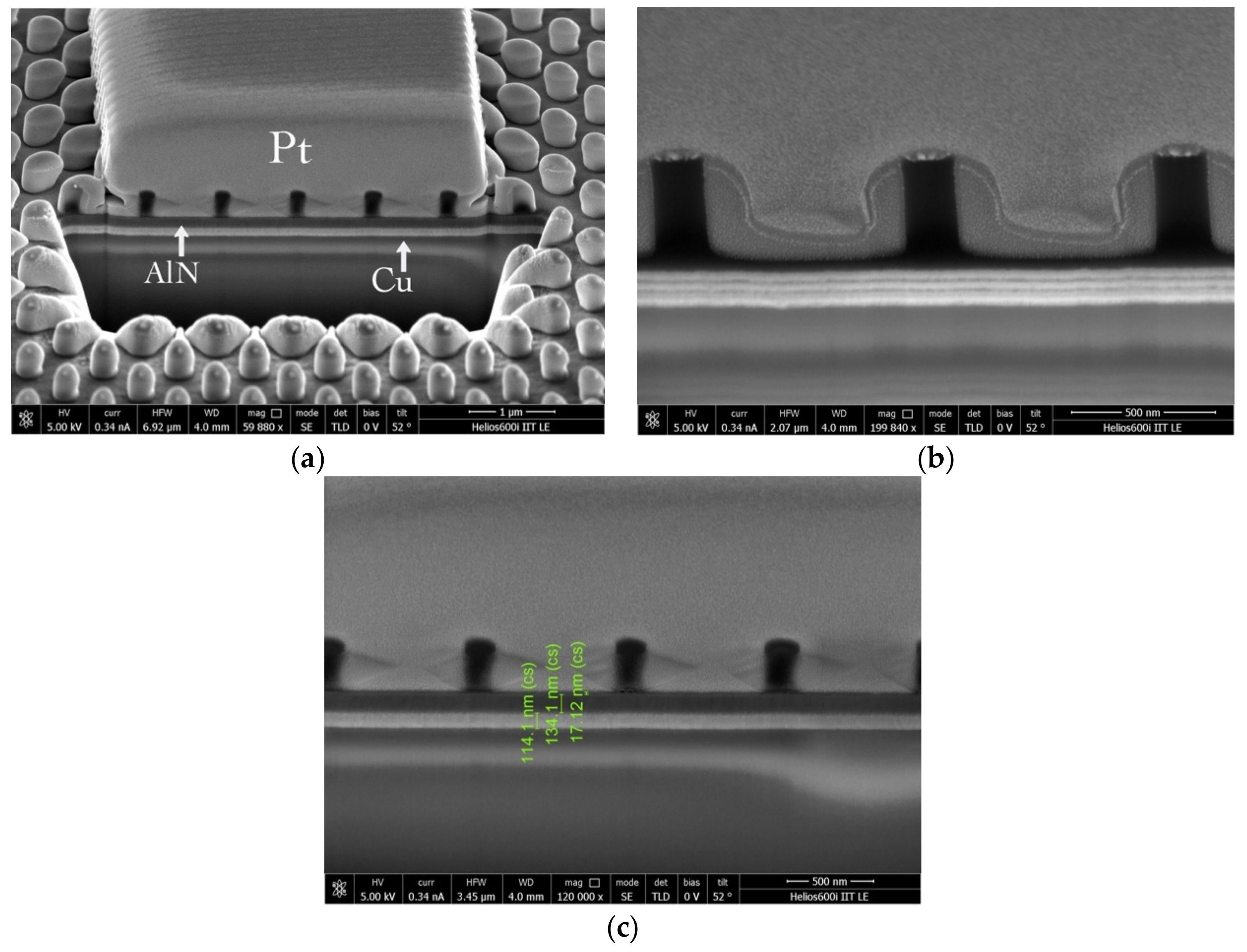
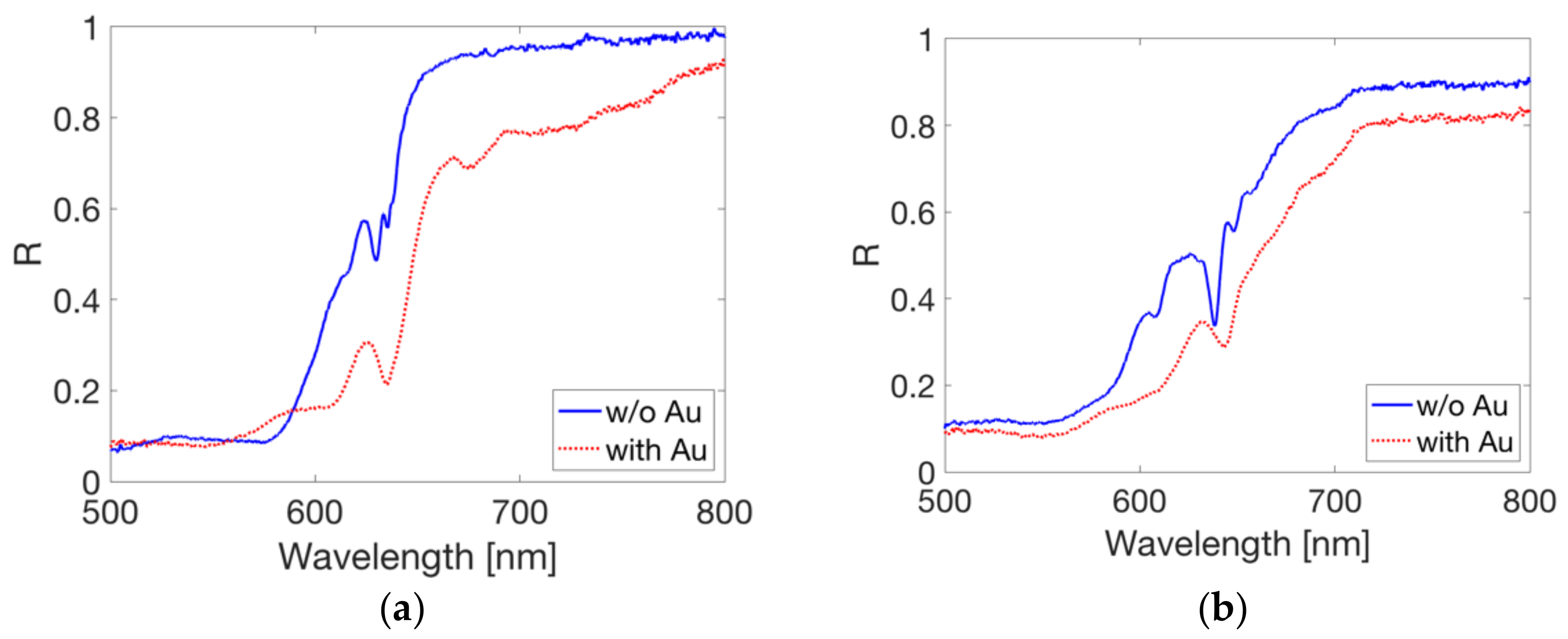
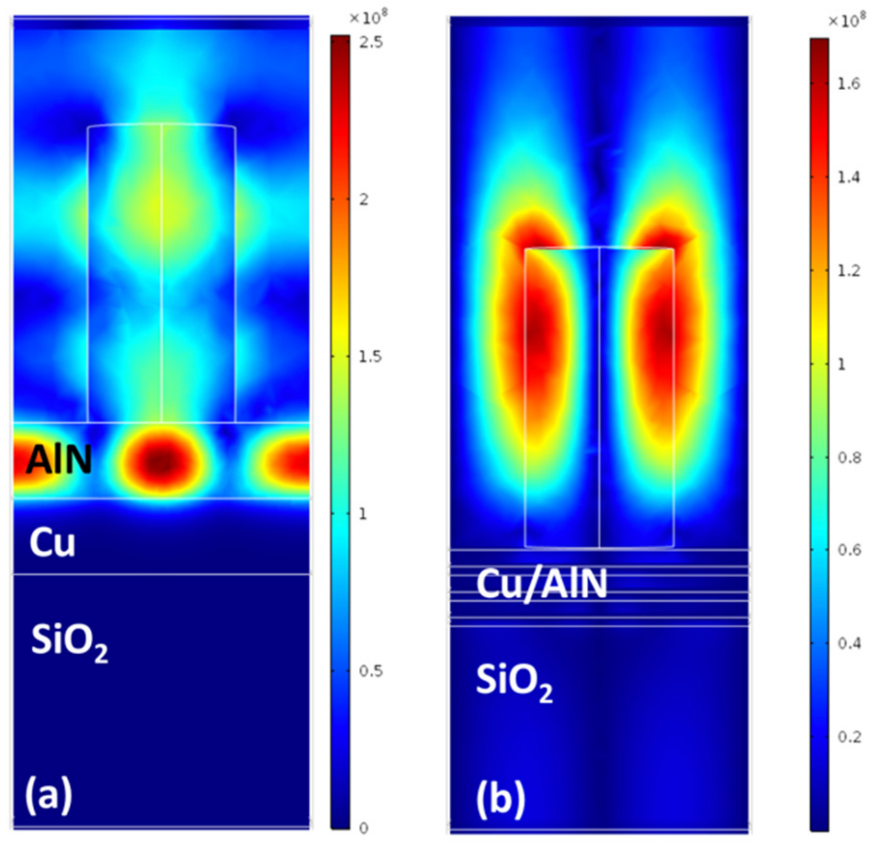
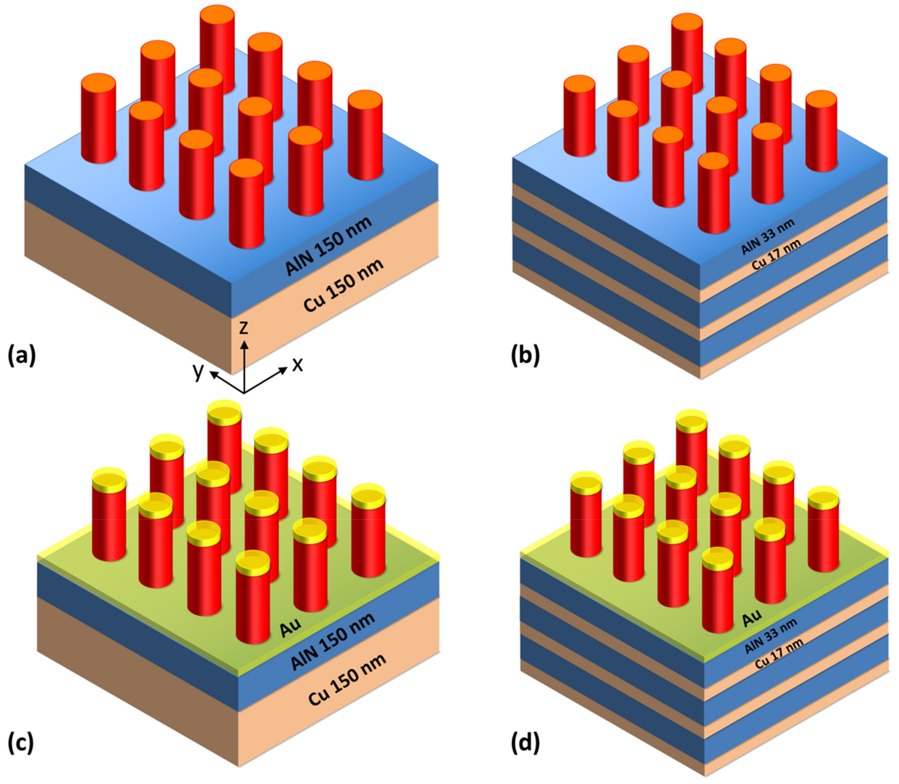
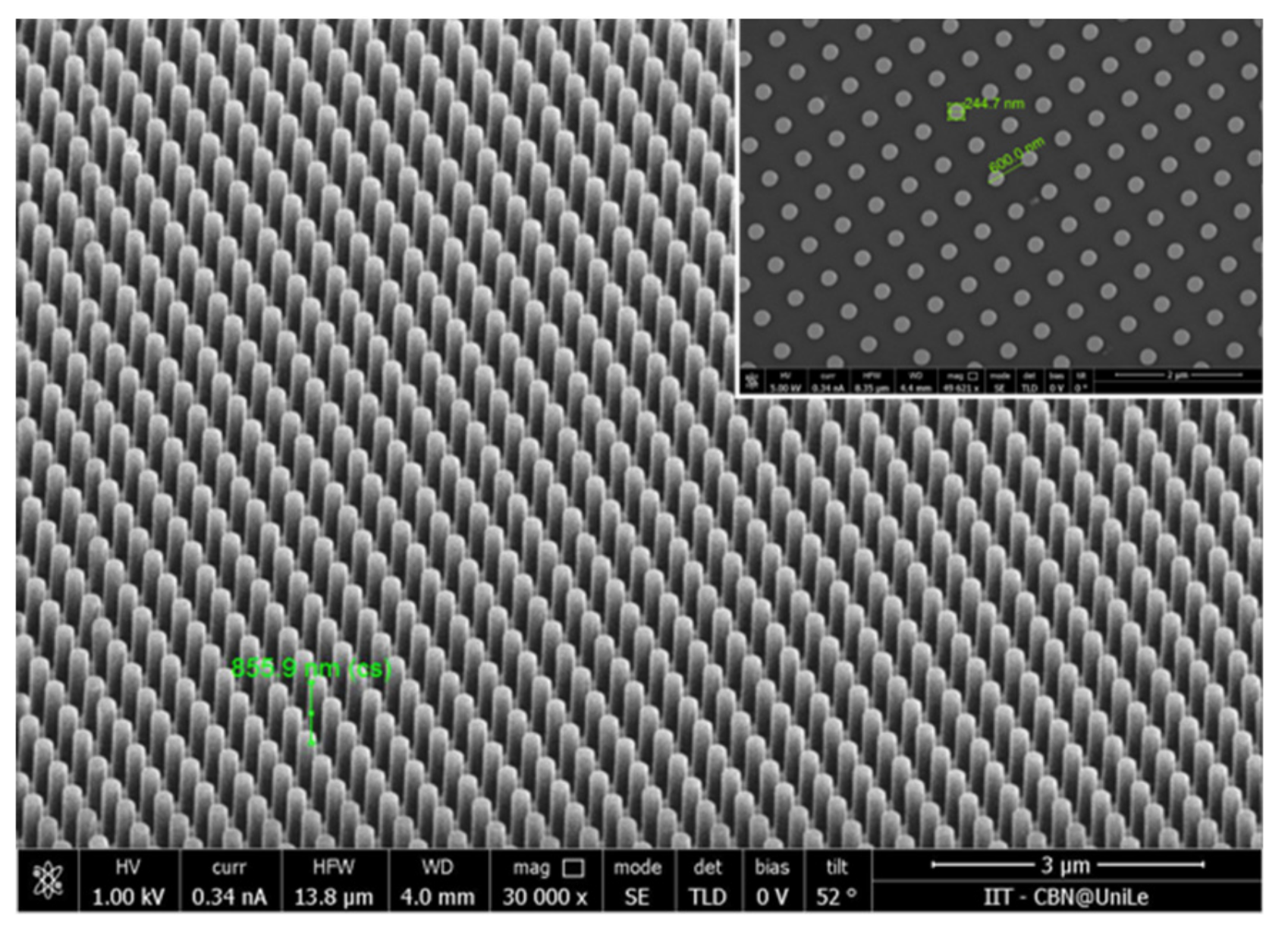
2. Results and Discussion

Figure 1 is a sketch of the proposed 2D array of PMMA pillars deposited on different configurations of Cu/AlN slabs supported by a SiO2 substrate. In particular, Figure 1a,b correspond to the bilayer and multilayer, respectively. The arrays show a square lattice with a periodicity p equal to 450 and 600 nm. The square lattice makes the device polarization-insensitive at normal incidence. Without loss of generality, hereinafter, we will consider three pairs of metallo-dielectric slabs for the multilayer configuration.
The Cu/AlN bilayer and multi-layer structures were deposited by a DC magnetron sputtering technique (K.J. Lesker Lab 18 system) without a preheating process of the substrate and performed in a single run of deposition in order to minimize contaminations between the layers. A SiO2 test sample was used to optimize the thickness of the sputtered materials. The growth conditions were optimized to provide good adhesion properties, high crystallographic quality, low residual stress, and well-controlled deposition rates. In more detail, starting from a base pressure of about 10−7 mbar, the Cu layers were sputtered from a high-purity Cu target (99.95%), in an Ar atmosphere at a working pressure of 5 × 10⁻³ mbar and a power of 200 W, with a deposition rate of 0.28 nm/s. The AlN layers were deposited from a high-purity Al target (99.9995%) with a gas mixture of N2/Ar (1:1 gas ratio) at a working pressure of 2.8 × 10⁻³ mbar; the sputtering plasma was generated in pulsed mode with a frequency of 100 kHz and a power of 1000 W, showing a deposition rate of 0.55 nm/s. Thicknesses were verified by scanning electron microscope (SEM) inspection. The cross-section of the sputtered materials was investigated by means of a focused ion beam (FIB) system that calculated the slab thicknesses (Figure 2). The grey area on the top of the AlN film refers to the platinum (Pt) deposition used to protect the sample during the milling with FIB (Figure 2a) while Figure 2b shows the measured thicknesses of the Cu (about 100 nm) and AlN (about 150 nm) layers deposited on the test SiO2 substrate.
Based on these results, a stack composed of three alternating couples of Cu (17 nm-thick) and AlN (33 nm-thick) deposited on a SiO2 substrate was achieved.
Subsequently, sub-micron PMMA pillars were realized using the nanoimprint lithography technique (EITRE® 3 system – Obducat Technologies AB, Malmo, Sweden). A silicon mold was used in the NIL process consisting of two square arrays of holes ≃ 900 nm depth, with a total footprint of 2.5 mm × 2.5 mm. After the molds were fabricated, they were coated with a commercial anti-sticking layer that facilitates the subsequent de-molding process. In order to optimize the NIL process, several tests were performed by varying the temperature (in the range 170–180 °C) and pressure (in the range 30–40 bar), allowing us to achieve uniform and high-resolution pillars starting with a PMMA layer thickness of 220 nm. The system heats up the substrate and the mold at the same time and the same temperature.
Figure 3 shows the bird’s eye and in-plane (inset) SEM image of the 2D array of PMMA pillars fabricated with p = 600 nm and diameter of about 250 nm when temperature and pressure were set equal to 180 °C and 40 bar.
By using the two optimized technologies, i.e., the sputtering and the NIL, we easily realized dielectric gratings deposited on AlN/Cu slabs that support optical resonances. Figure 4a shows the cross-section of the fabricated bi-layer structure where the thicknesses of Cu and AlN are set equal to 100 nm and 150 nm, respectively, while the pillar diameter is equal to 250 nm.
We covered the fabricated structures with a thin gold layer (thickness equal to about 15 nm) deposited by means of a process of 40 s sputtering with a gold target in order to inspect them by means of the SEM. Figure 1 shows the areas covered by gold at the bottom and on the top of the periodic pillars pattern.
Figure 4b shows the SEM picture of the 2D pillar array on the multi-layer structure with the same periodicity. All the sizes comply with the design providing the right thicknesses of Cu and AlN (17 nm and 33 nm, respectively). It is worth stressing that the SEM image also determined the thickness of the PMMA buffer layer equal to about 20 nm (Figure 4c).
All the fabricated devices, with and without gold, were optically characterized by means of an ad hoc setup, where the reflected light by the sample at normal incidence was analyzed by an integrated spectrometer [9,10]. Figure 5 shows the comparison between the reflection spectra of both configurations without and with the gold layer, for the bilayer (Figure 5a) and the multilayer (Figure 5b), respectively. The plots reveal that, when the gold layer is taken into account, the resonance dip shifts from 629.8 nm to 634.9 nm (bilayer) and from 638.5 nm to 643.3 nm. Therefore, the shift is almost the same (5.1 nm vs. 4.8 nm) for both configurations. Conversely, the reflectance at the dip minimum drops from 49% to 21% (difference about 28%) and from 33% to 29% (difference equal to 4%) for the bilayer and multilayer, respectively. It is worth noting that the full width at half maximum (FWHM) slightly increases due to the presence of the plasmonic material for both configurations. In particular, the FWHM of resonance for the bilayer configuration changes from about 4 nm to 7 nm while it varies from about 5 nm to 8 nm in the case of the multilayer configuration when the gold layer is added. Finally, if we consider the reflectance in the wavelength range where the structures act as mirrors, we can verify that the values drop about 20% and 8% for the two cases, respectively, leading to a reduction of a factor of 2.5.
Considering the absorption as A = 1 − R, it is possible to conclude that the control of the absorption is improved by exploiting the metallo-dielectric slab. It is also worth highlighting that by just adding a thin gold layer it is possible to increase the total absorption. Indeed, the gold layer introduces more optical losses due to the plasmonic nature of the Au film. This is evident from the experimental results reported in Figure 5.
Although the paper is mainly focused on the experimental validation of the fabrication protocol and optical characterization, we also performed a numerical analysis by exploiting 3D numerical models (COMSOL, Inc., Burlington, MA 01803, USA) that describe the bilayer/multilayer configurations. In particular, Figure 6a,b show the electric field profile of the x-component in the x-z plane for both configurations at the resonance dips depicted in Figure 5 (solid blue curves). From these plots, it is possible to verify that the main difference is related to the field distribution that for the bilayer configuration (a) is mainly localized in the Al slab as expected for the GMRs. Conversely, in the multilayer configuration (b), the electric field is more concentrated at the air–PMMA interface since the metallo-dielectric multi-layer acts as a mirror. This feature could be efficiently exploited for sensing applications where the gold layer could be functionalized.

3. Conclusions

We reported on the fabrication and optical characterization of a 2D pillar pattern deposited on AlN/Cu slabs. In particular, the proposed nano-technological protocol can easily realize dielectric gratings that support guided-mode resonances with spectral features showing FWHM in the order of a few nanometers. We compared the performance of a bilayer configuration (single pair) that supports GMRs with that of a multi-layer configuration where the guiding slab is substituted by a metallo-dielectric pair.
We also investigated the same configurations covered by a thin gold layer. The metallo-dielectric structure with gold could be exploited for the realization of optical sensors based on hyperbolic metamaterials as reported in [23]. These results can lead to the fabrication of hybrid devices that take advantage of the excellent properties of both photonic and plasmonic resonances for a wide plethora of applications spanning from sensing, surface-enhanced Raman spectroscopy (SERS) to optical nonlinear-based devices. Finally, the possibility to integrate two-dimensional materials, such as graphene, in the proposed structure could lead to the realization of tunable fabrication-tolerant and robust photonic devices [24].

Author Contributions

T.S. and M.G. prepared the original draft. F.G. and A.C. grew the samples. A.C. and T.S. fabricated the final structures by means of NIL. A.Q. and T.S. acquired the SEM images. M.S., M.D.V., A.D., T.S., and M.G. contributed to the review and editing of the paper.

Funding

This research received no external funding.

Conflicts of Interest

The authors declare no competing interests.

References

  1. Kats, M.A.; Capasso, F. Optical absorbers based on strong interference in ultra-thin films. Laser Photon. Rev. 2016, 10, 735–749. [Google Scholar] [CrossRef]
  2. Magnusson, R.; Wang, S.S. New principle for optical filters. Appl. Phys. Lett. 1992, 61, 1022–1024. [Google Scholar] [CrossRef]
  3. Lu, G.; Wu, F.; Zheng, M.; Chen, C.; Zhou, X.; Diao, C.; Liu, F.; Du, G.; Xue, C.; Jiang, H.; et al. Perfect optical absorbers in a wide range of incidence by photonic heterostructures containing layered hyperbolic metamaterials. Opt. Express 2019, 27, 5326–5336. [Google Scholar] [CrossRef] [PubMed]
  4. Lin, H.; Sturmberg, B.C.; Lin, K.T.; Yang, Y.; Zheng, X.; Chong, T.K.; de Sterke, C.M.; Jia, B. A 90-nm-thick graphene metamaterial for strong and extremely broadband absorption of unpolarized light. Nat. Photon. 2019, 13, 270–276. [Google Scholar] [CrossRef]
  5. Zhu, H.; Yi, F.; Cubukcu, E. Plasmonic metamaterial absorber for broadband manipulation of mechanical resonances. Nat. Photon. 2016, 10, 709–714. [Google Scholar] [CrossRef]
  6. Sreekanth, K.V.; ElKabbash, M.; Alapan, Y.; Rashed, A.R.; Gurkan, U.A.; Strangi, G. A multiband perfect absorber based on hyperbolic metamaterials. Sci. Rep. 2016, 6, 26272. [Google Scholar] [CrossRef] [PubMed] [Green Version]
  7. Fan, Y.; Guo, C.; Zhu, Z.; Xu, W.; Wu, F.; Yuan, X.; Qin, S. Monolayer-graphene-based broadband and wide-angle perfect absorption structures in the near infrared. Sci. Rep. 2018, 8, 13709. [Google Scholar] [CrossRef]
  8. Mahigir, A.; Veronis, G. Nanostructure for near total light absorption in a monolayer of graphene in the visible. J. Opt. Soc. Am. B 2018, 35, 3153–3158. [Google Scholar] [CrossRef]
  9. Grande, M.; Vincenti, M.A.; Stomeo, T.; Bianco, G.V.; de Ceglia, D.; Aközbek, N.; Petruzzelli, V.; Bruno, G.; De Vittorio, M.; Scalora, M.; et al. Graphene-based perfect optical absorbers harnessing guided mode resonances. Opt. Express 2015, 23, 21032–21042. [Google Scholar] [CrossRef]
  10. Grande, M.; Vincenti, M.A.; Stomeo, T.; Bianco, G.V.; de Ceglia, D.; Aközbek, N.; Petruzzelli, V.; Bruno, G.; De Vittorio, M.; Scalora, M.; et al. Graphene-based absorber exploiting guided mode resonances in one-dimensional gratings. Opt. Express 2014, 22, 31511–31519. [Google Scholar] [CrossRef]
  11. Kashif, M.F.; Bianco, G.V.; Stomeo, T.; Vincenti, M.A.; de Ceglia, D.; De Vittorio, M.; Scalora, M.; Bruno, G.; D’Orazio, A.; Grande, M. Graphene-based cylindrical pillar gratings for polarization insensitive optical absorbers. Appl. Sci. 2019, 9, 2528. [Google Scholar] [CrossRef]
  12. Zhang, W.; Chou, S.Y. Fabrication of 60-nm transistors on 4-in. wafer using nanoimprint at all lithography levels. Appl. Phys. Lett. 2003, 83, 1632. [Google Scholar] [CrossRef]
  13. Koo, N.; Schmidt, M.; Mollenhauer, T.; Moormann, C.; Schlachter, F.; Kurz, H. Fabrication of MOSFETs by 3D soft UV-nanoimprint. Microelecton. Eng. 2012, 9, 85. [Google Scholar] [CrossRef]
  14. Pisignano, D.; Persano, L.; Gigli, G.; Visconti, P.; Stomeo, T.; De Vittorio, M.; Cingolani, R. Planar organic photonic crystals fabricated by soft lithography. Nanotechnology 2004, 15, 766–770. [Google Scholar] [CrossRef]
  15. Meng, F.; Luo, G.; Maximov, I.; Montelius, L.; Chu, J.; Xu, H. Fabrication and characterization of bilayer metal wire-grid polarizer using nanoimprint lithography on flexible plastic substrate. Microelectron. Eng. 2011, 88, 3108. [Google Scholar] [CrossRef]
  16. Zhu, S.; Li, H.; Yang, M.; Pang, S.W. High sensitivity plasmonic biosensor based on nanoimprinted quasi 3D nanosquares for cell detection. Nanotechnology 2016, 27, 295101. [Google Scholar] [CrossRef]
  17. Zhou, J.; Tao, F.; Zhu, J.; Lin, S.; Wang, Z.; Wang, X.; Ou, J.Y.; Li, Y.; Liu, Q.L. Portable tumor biosensing of serum by plasmonic biochips in combination with nanoimprint and microfluidics. Nanophotonics 2019, 8, 307–316. [Google Scholar] [CrossRef]
  18. Lee, S.W.; Lee, K.S.; Ahn, J.; Lee, J.J.; Kim, M.G.; Shin, Y.B. Highly sensitive biosensing using arrays of plasmonic Au nanodisks realized by nanoimprint lithography. ACS Nano 2011, 5, 897–904. [Google Scholar] [CrossRef]
  19. Ou, F.S.; Naumov, M.H.I.; Kim, A.; Wu, W.; Bratkovsky, A.M.; Li, X.; Williams, R.S.; Li, Z. Hot-spot engineering in polygonal nanofinger assemblies for surface enhanced Raman spectroscopy. Nanoletters 2011, 2538–2542. [Google Scholar] [CrossRef]
  20. Chou, S.Y.; Krauss, P.R.; Renstrom, P.J. Imprint lithography with 25-nanometer resolution. Science 1996, 272, 85–87. [Google Scholar] [CrossRef]
  21. Marani, R.; Marrocco, V.; Grande, M.; Morea, G.; D’Orazio, A.; Petruzzelli, V. Enhancement of extraordinary optical transmission in a double heterostructure plasmonic bandgap cavity. Plasmonics 2011, 6, 469–476. [Google Scholar] [CrossRef]
  22. Grande, M.; Stomeo, T.; Bianco, G.V.; Vincenti, M.A.; de Ceglia, D.; Petruzzelli, V.; Bruno, G.; de Vittorio, M.; Scalora, M.; D’Orazio, A. Fabrication of doubly resonant plasmonic nanopatch arrays on graphene. Appl. Phys. Lett. 2013, 102, 231111. [Google Scholar] [CrossRef]
  23. Sreekanth, K.V.; Alapan, Y.; ElKabbash, M.; Ilker, E.; Hinczewski, M.; Gurkan, U.A.; De Luca, A.; Strangi, G. Extreme sensitivity biosensing platform based on hyperbolic metamaterials. Nat. Mater. 2016, 15, 621–627. [Google Scholar] [CrossRef] [PubMed] [Green Version]
  24. De Ceglia, D.; Vincenti, M.A.; Grande, M.; Bianco, G.V.; Bruno, G.; D’Orazio, A.; Scalora, M. Tuning infrared guided-mode resonances with graphene. J. Opt. Soc. Am. B 2016, 33, 426–433. [Google Scholar] [CrossRef]
Figure 1. (a,b) Sketch of fabricated samples with an array of cylindrical pillars on top of (a) bilayer and (b) multilayer configurations (three pairs), respectively. (c,d) Sketch of the (c) bilayer and (d) multilayer configurations, respectively, covered by a thin gold layer.
Applsci 09 03812 g001
Figure 2. (a) Scanning electron microscope (SEM)scan showing the cross-section of bilayer design. Grey area on the top of aluminum nitride (AlN) film is a Pt deposition used to protect layers while milling with focused ion beam (FIB). (b) Cu (about 100 nm) and AlN (about 150 nm) layer thicknesses deposited on a test SiO2 substrate. The measured thicknesses are corrected for the tilt.
Applsci 09 03812 g002
Figure 3. Bird’s eye SEM image of the fabricated device; (inset) in-plane detail of the fabricated 2D polymethyl-methacrylate (PMMA) plasmonic nano-pillar array. The measured pillar height is corrected for the tilt.
Applsci 09 03812 g003
Figure 4. SEM images related to the cross-section of (a) bilayer and (b) multi-layer designs, respectively. Cu, AlN layers and PMMA pillars (black region) while the grey area around pillars is a Pt deposition used to protect the sample while milling with FIB. (c) Cross-section of the bilayer sample revealing the PMMA buffer layer thickness equal to about 20 nm.
Applsci 09 03812 g004
Figure 5. Measured reflectance spectra of both configurations without (solid blue line) and with a gold layer (dashed red curve), for (a) the bilayer and (b) the multilayer, respectively.
Applsci 09 03812 g005
Figure 6. Electric field profile of the Ex component in the x-z plane for the (a) bilayer and (b) multilayer configurations at the operating wavelength equal to 645 nm and 624 nm, respectively. The impinging electric field is along the x-axis (Figure 1).
Applsci 09 03812 g006

