Thin Coatings of Cerium Oxide Nanoparticles with Anti-Reflective Properties
by
 and
and
Laura J. Romasanta
1, 
Lauriane D’Alençon
2,
Sara Kirchner
3,
Christophe Pradère
3 and
Jacques Leng
1,* 1
University of Bordeaux, Laboratory of the Future (CNRS/SOLVAY), 178 avenue du Docteur Schweitzer, 33600 Pessac, France
2
Solvay, Functional Inorganic Materials Laboratory, 52 rue de la Haie coq, 93300 Aubervillliers, France
3
Institut d’ingénierie et de mécanique, TREFLE, Esplanade des Arts et Métiers, 33400 Talence, France
*
Author to whom correspondence should be addressed.
Appl. Sci. 2019, 9(18), 3886; https://doi.org/10.3390/app9183886
Submission received: 30 July 2019
/
Revised: 2 September 2019
/
Accepted: 5 September 2019
/
Published: 16 September 2019
(This article belongs to the Special Issue Advances in Organic Corrosion Inhibitors and Protective Coatings)
Abstract
:Cerium oxide, in addition to its catalytic properties, is also known for its optical properties such as ultraviolet (UV) radiation filtering and a relatively high refractive index (), which makes it an excellent candidate for multifunctional coatings. Here, we focus on the optical properties of thin deposits (≲2m) of densely packed nanoparticles, which we assemble using two evaporation-based techniques: convective self-assembly (CSA, a type of very slow blade-coating) to fabricate large-scale coatings of controllable thickness—from tens of nanometres to a few micrometers—and microfluidic pervaporation which permits us to add some micro-structure to the coatings. Spectroscopic ellipsometry yields the refractive index of the resulting nano-porous coatings, which behave as lossy dielectrics in the UV-visible regime and loss-less dielectrics in the visible to infra-red (IR) regime; in this regime, the fairly high refractive index (≈1.8) permits us to evidence thickness-tunable anti-reflection on highly refractive substrates, such as silicon, and concomitant enhanced transmissions which we checked in the mid-IR region.

1. Introduction
Cerium oxide nanoparticles have been applied in diverse fields including catalysis, luminescence, and nanomedicine, etc. [1,2,3]. Here, we investigate their optical behaviour when assembled as coatings onto a substrate. As cerium oxide () has a fairly high optical refractive index, we expect that dense coatings made out of nanoparticles will also exhibit a high refractive index.
We follow a low-tech approach to engineer simple coatings out of dispersions of nanoparticles. The coatings are realized using evaporation-based techniques out of water-based dispersions, making the processes fairly appealing in terms of energy consumption and toxicity: Their fabrication requires virtually no external pressure, no toxic or hazardous gases, no elevated temperatures, no etching, no vacuum, and no toxic solvents. The coatings we obtain have simple yet non trivial structures and they perform very well from an optical point of view, in particular for anti-reflection on highly refractive materials, which we demonstrate on silicon as a case study.
First, we re-demonstrate that the evaporation-based blade-coating method is efficient for producing coatings of controllable thickness, in this case, out of dispersions. These results conform to the pioneering work of O. Velev and co-workers [4,5] who coated dispersions on glass and silicon. The very slow regime of blade-coating, were evaporation competes favourably with the casting velocity enhances the formation of a well structured, thin to thick deposit. We also add some complexity via micro-patterned structures using an evaporation-based micro moulding technique. We measure the refractive index of these coatings which behave as lossy dielectrics in the ultraviolet (UV)-visible regime and loss-less dielectrics in the visible to infra-red (IR) regime; in the latter regime, the fairly high refractive index (≈1.8) permits us to demonstrate thickness-tunable anti-reflection properties on substrates with a high refractive index such as silicon substrates, and concomitant enhanced transmission which we tested in the mid-IR region, thereby covering a large spectral range.
2. Thin and Structured Coatings of Densely Packed Nanoparticles
We use two different techniques that permit us to assemble an initially dispersed state of nanoparticles into a solid made of the same, densely packed nanoparticles: convective self-assembly (CSA) and microfluidic pervaporation (-pervaporation). A detailed description of these methods will be given in Section 4.2.
In brief, CSA is a modified blade-coating technique where the withdrawing velocity of the substrate on which the coating will be deposited is so small that evaporation competes with the film casting rate, so that the dispersion is pre-concentrated at the level of the deposition meniscus; on top of this, it enhances the structure of the deposit [6,7,8,9].
-pervaporation takes advantage of the extremely well-defined poly(dimethyl siloxane) (PDMS) geometries crafted by soft-lithography [10,11], as well as the ability of some solvents to pervaporate across the elastomer PDMS matrix [12]. Pervaporation induces a concentration mechanism of the solute, which was initially solubilized/dispersed in the solvent, thus leading to the formation of a solid that grows in a neat geometry [13]. It is an ‘augmented’ version of the moulding of solids into micro-capillaries, a seminal and inspiring piece of work described in [14].
2.1. Convective Self-Assembly
CSA has been extensively used to deposit a variety of objects (from molecules [15] to large colloids [6]) into homogeneous thin coatings on relatively large scales (tens of cm). It is possible to control the thickness and to some extent the morphology of the coating via process parameters such as the casting velocity, the concentration of the stock solution [16], temperature, humidity, etc., but also to couple the reaction to the deposition process, for instance for sol-gel coatings [17], and finally to stop and re-run the process (stop-and-go), in order to add more structure to the deposit [18].
Here, we use the simplest version of CSA, namely a continuous and slow deposition of a dispersion at constant volume fraction at room temperature and with no specific control of the atmosphere (the room in which we work is nevertheless air-conditioned with a constant temperature 21 C and relative humidity ≈0.5). The air flow over the evaporating zone is not controlled and is left to natural convection; it has been demonstrated that for the deposition colloids and unlike the case of polymers, it is not a crucial parameter [7]. The only control parameter we use is the casting velocity v; we deposit the same grade of nanoparticles with batches coming at two different typical sizes: ≈4 and ≈40 nm (average diameter, see Section 4.1).
The overview of our deposition campaigns is summarized in Figure 1 with the coating thickness, the morphology of the coatings, and their optical appearance. In the velocity range of deposition we studied (m.s), the decreasing trend of h against v is a clear signature of the CSA regime and with a comparable behaviour for the two sizes of nanoparticles studied here; it contrasts with the Landau-Levich regime where h is expected to scale like [15].
However, the coating is not always homogeneous and flat, see Figure 2 top and the grey and blue zones in Figure 1, bottom left. Instead, for the large particles and at low deposition velocity (v ≲ 40m.s) the coating exhibits thickness oscillations. Notice this is definitely not stick-and-slip [19] but instead oscillations around a mean (non zero) thickness with no return to the bare substrate. At even lower velocity (v ≲ 10m.s), the coating delaminates, probably because it becomes thick, tough and brittle [20]. For the small-size particles, we observe only thickness oscillations below v ≲ 10m.s (blue zone in Figure 1, bottom left).
The same data can be re-scaled using a simple mass-conservation assumption (Equation (3) simply states that all the particles coming from the bulk reservoir are accumulated into the final deposit via evaporation), that takes into account both the initial and final volume fractions, and respectively. Using a value that we obtained from ellipsometry, which is in agreement with a close packing of a polydisperse hard-sphere [21], the data reasonably collapse and follow the expected trend indeed.
In all cases but the ones where the coatings delaminate, the coated substrate appears perfectly transparent with no visible effect of surface undulations and no haze (upper inserts in Figure 1), even though optical microscopy reveals the defects (Figure 2 top). Low resolution scanning electron microscopy (SEM) of the surface of some samples may show evidence of the granulometry of the particles (Figure 2 bottom left) but a cross-section of a selected sample demonstrates a beautiful, flat, and large-scale structure (Figure 2 bottom right).
2.2. Microfluidic Pervaporation
Microfluidic pervaporation is a templated self-assembly method [22] where a PDMS mould—the template—is used to guide the growth of a solid made of nanoparticles. In turn, the template also serves as a pump via the pervaporation mechanism described more in detail in Section 4.2. The process is self-powered: We fill the microfluidic template with a dilute dispersion and pervaporation extracts the solvent, which in turn concentrates the dispersion until a solid nucleates, which then progressively grows. It can be a long process as the growth velocity can be understood on a simple volume conservation assumption, very similar to Equation (3): where is an evaporation velocity associated with the pervaporation mechanism [12,23]. It offers little flexibility as it is mainly governed by the geometry of the template, i.e., surface exchange for pervaporation, yet the growth velocity is still largely tunable via . We typically see m.s which permits us to fill the entire length of the template in about one day. It is slow mostly because the stock solution is dilute, , and much slower than CSA (m.s, Figure 1) because the evaporation proceeds across the PDMS template, not directly in air.
In general, the solid we obtain nicely replicates the shape of the mould [13]. However, we discovered fairly recently that there are cases where the solid significantly deforms the template during its growth [24]. It is likely due to a poro-elastic mechanism related to the depression generated inside the material, originating from the suction mechanism during the evaporation-induced growth [25].
We deliver here the very same observation: Whereas the mould has a nominal thickness of ≈3m, the final material barely reaches h ≈ 300 nm, see Figure 3. We understand it on the basis of the small size of particles, here ≈4 nm, which generates a massive pressure drop inside the material during the growth of the solid upon evaporation that tends to collapse the soft PDMS template. It is somewhat disappointing as we targeted thick deposits, but the final material turns out to be fairly flat (Figure 3). Altogether, this method mainly leads to arbitrarily structured coatings which are impossible to obtain with CSA only and where the structure could bring some additional function.
3. Optical Features of Nanoporous Coatings
3.1. Refractive Index
Variable angle spectroscopic ellipsometry (VASE) was used to measure the refractive index of the coatings and we limited ourselves to coatings made of the thinnest grade of nanoparticles where the final material does significantly scatter the light (empirical observation). VASE provides ellipsometric raw data (here and angles) that need to be parametrized in order to extract the complex refractive index [26].
The optimisation approach requires knowledge of the refractive index of nanoparticles, their packing density inside the coating ( being the void fraction or porosity), and the thickness of the coating h. We then compute the ellipsometric angles of the coating with a refractive index calculated via the Bruggeman effective-medium approximation [27] of a flat nano-porous film with no roughness and deposited of a semi-infinite silicon substrate with an oxidized top surface, namely a 2 nm thick silica layer.
To guide the input parameters, we used the coating thickness measured by mechanical profilometry ( nm), the packing density of a random close packing structure, and the refractive index based on literature data [28] and parametrized according to [29]. The optimisation is then performed through the Horiba software and eventually yields , nm, a model of (not shown), and ultimately, a very good agreement with ellipsometric raw data (Figure 4 left). The refractive index of nanoparticles is comparable yet smaller in magnitude than bulk cerium oxide, which could be attributed to a synthetic route that is likely to lead to a material different from bulk .
We thus obtain a satisfactory measurement of the refractive index of the nanoporous coating of on a specific range of photon energy ( eV, i.e., nm, Figure 4): shows a significant absorption of light in the UV-visible regime up to nm where the material becomes a loss-less dielectric with , . We assume it remains true even up to the mid-IR range, for instance m, which we will also use to characterize the transmittance of the coating in this regime.
Also, we assume that this measurement obtained on a specific coating is intrinsic and thus holds, whatever the thickness of a homogeneous coating made out of the same grade of particles.
3.2. Reflection Features on Silicon Substrates
Light reflection is due to a refractive index mismatch at an interface between two different media. The reflectance is the ratio between the reflected intensity over the incident intensity of light and can be calculated using the Fresnel equation at normal incidence as follows: where the s stand for the refractive indices of the two media, and which also holds when the refractive indices are complex values. As an example, silicon in air () displays a reflectance of around in the visible to near-infrared range, see the dashed blue line in Figure 5.
An anti-reflective coating (ARC) with an adequate refractive index and thickness can lower this light reflection at an interface between two different media. The simplest ARC with a refractive index leading to at normal incidence and at a single wavelength of incident radiation is obtained at a thickness when . More precisely, such a result is obtained through the calculation of the multi-layer reflection coefficient based on r, the amplitude Fresnel coefficient of a three-layer stack where layer 1 stands for air (refractive index , semi-infinite), layer 2 stands for the coating, and layer 3 is the semi-infinite substrate [30,31]:
with the phase shift in the coating of thickness h, and and the amplitude Fresnel coefficients at interfaces between media 1 and 2, and 2 and 3 respectively. Notice that the s may admit complex values. Here, medium 1 is air (), medium 2 is the nanoporous coating (see Figure 4 right for ), and layer 3 is the silicon substrate ( found in Reference [32]).
We performed the characterization of intensity reflectance R under normal incidence of light in the range nm with bench-top, fairly basic equipment; the main limitation of our set-up comes from the illumination and collection of optical fibres which do not work exactly at normal incidence but accommodate some angular opening, which is somewhat detrimental to the fine measurement of R. Figure 5 shows measurements of R vs when the coating is deposited on the polished side of a silicon wafer. Here, we show the results for coatings with four different thickness (red curves) along with the reference reflectance of the bare silicon substrate (blue dashed curve) and the calculated reflectance, black curve with Equation (1).
In all cases, the reflectance is lowered by the presence of the coating (Figure 5), and for the three thickest coatings, it even exhibits a vanishing reflectance at several wavelengths, which expectingly increase with the thickness of the coating. Owing to the absence of a fitting parameter, the agreement between the experiments and the calculation is satisfactory, especially in the visible to near-IR range. The slight discrepancy that shows for the thickest coating could be due to the fact that we are not working at a perfect normal incidence.
3.3. Enhanced Transmission on Silicon Substrates
Along with anti-reflection behaviour comes a possible enhanced transmission provided by the ARC. Now, we work with a bare substrate which has two polished sides and which is thick enough (m) to exhibit an incoherent behaviour [30], so that we can neglect the interferences. We nevertheless take into account the multiple reflections for calculating the total optical path from which the total transmittance follows:
with R is the reflectance at the different interfaces where subscripts A, C, and S stand for air, coating, and substrate respectively, is the extinction coefficient in the substrate with as the imaginary part of the refractive index of the substrate of thickness L. and are calculated following the procedure of Equation (1); in the case of a bare substrate, replace and with .
We measured the transmission T of a two-sided polished substrate coated with a micro-structured pattern using a spectro-imaging set-up (described in Section 4.4 and in [33,34]). Owing to the imaging capability of the device, it is possible to select the measurement place in a heterogeneous sample such as ours, see Figure 6A with a spatial resolution of about m in this specific case, but which depends on the magnification. We thus performed a reference measurement on the bare substrate, the result of which is shown in Figure 6B (blue symbols) and which agrees well with the calculated Equation (2) and tabulated values [32] (blue line). We notice a residual peak at m which we attribute to absorption, and which we have difficulty in systemically removing. When the measurement was performed and averaged on a specific part of the pattern—namely the bright lines of Figure 6A—we observed a significant increase of transmittance, see the red symbols of Figure 6B, and which is parametrized with Equation (2) where the thickness h of the coating is left as a free parameter in the range 300–600 nm. It is clear that the experimental transmission is properly framed by the calculated T although the best agreement is found for nm which does not perfectly match the actual thickness nm. The slight discrepancy could be due either to the fact that the sample is actually slightly slanted and not perfectly perpendicular to the incident beam, or possibly also that the pixel size of the imaging set-up (≈25m) is not very small compared to the width of the pattern ≈100m), which could induce some ’blurring’ in the measured transmittance. Yet, it definitely corroborates that the anti-reflection coating is accompanied with an enhanced transmission; such a coating could thus be used to enhance the silicon transmission when this material is used as an optical component for mid-IR imaging purposes for instance, and is particularly efficient at some specific wavelengths but is obviously wavelength dependent, see Section 5.
4. Materials And Methods
4.1. Dispersions of Nanoparticles
Fairly monodisperse cerium oxide () nanoparticle dispersions were synthesized and kindly provided by Solvay with two grades: a small diameter ( nm) at volume fraction , , and a large diameter ( nm) at volume fraction , , see Figure 7. These acidic dispersions are formulated in water with acetic acid in order to ensure the long-term colloidal stability of the particles (month/years at 4 C) with no additional additives such as surfactants. Transmitted-electron microscopy (TEM EOL JEM 2200FS FEG HR 200 kV) observations reveal the polyhedral shape of the particles, along with a significant size range which was otherwise also estimated using dynamic light scattering (values given above). The dispersions are used as such for the assembly of the nanoparticles. Importantly, we also obtained the very same results concerning coatings, using a commercial dispersion available at Sigma-Aldrich (catalog number 289744-500g).
4.2. Assembly Methods
4.2.1. Films Obtained by Convective Self-Assembly (CSA)
Convective self-assembly (CSA) is a modified blade-coating technique where the withdrawing velocity of the substrate on which the coating will be laid (Figure 8) is so small that evaporation competes advantageously with the film drawing rate: both the meniscus and the wet film (deposited continuously due to the displacement of substrate with good wetting properties) act as suction pumps via evaporation that drag the nanoparticles in this confined zone to eventually build a dense film, which fully dries soon after [7,8,9]. The final thickness h of the film is controllable via the velocity v, the evaporation rate, the bulk volume fraction of the dispersion, shape of the meniscus, etc. From mass conservation and as a rough guide [6,35]:
where is the volume fraction of the dispersion in the reservoir, the one of the final deposit, and the volumetric evaporation rate per unit of length in the lateral direction, perpendicular to v (). Interestingly, the coating thickness increases with a decreasing v, which sustains the enhanced role of evaporation in order to pre-concentrate the dispersion at the level of the meniscus.
This regime differs from the so-called Landau-Levich (LL) regime where the withdrawing velocity v is fast enough that the deposited film remains liquid during deposition and dries afterwards. Here, the liquid film thickness increases with the velocity v due to enhanced viscous dissipation in the liquid film, and consequently, the thickness of the final deposit increases with v.
The transition between CSA and LL regimes as a function of velocity, concentration, evaporation rate, etc., lead to a V-shaped curve for h against v [15]: at low v and at high v. It has been largely explored both experimentally and theoretically but remains a debated issue subject to continuous improvements. In particular, there exist considerable differences for the drying mechanisms between molecular or polymeric solutions and colloidal dispersions; heterogeneous coatings are often observed but remain largely unexplained, e.g., stick-slip sparse coatings or continuous yet undulating coatings (Figure 2, top). Nevertheless, homogeneous coatings are also at stake (Figure 2, bottom).
In practice, a small volume of a dispersion of nanoparticles (L) is placed in between the static blade and the substrate which moves at a velocity v in the range of . Here, both the blade and the substrate are square-inches, 1 mm thick glass slides (Marienfield Ref. 11400420) which were super-cleaned via piranha treatment (20 min) followed by air plasma treatment (1 min), both performed in a clean room. Glass slides are exposed to air only at the time of setting up the CSA experiment.
4.2.2. Deposits Engineered with Microfluidic Pervaporation
Microfluidic Pervaporation combines the moulding in micro-capillary methods (MIMIC [14]) with the ability of the poly(dimethyl siloxane) (PDMS), to let solvents pervaporate (permeation followed by evaporation) across it, including water even though the PDMS is hydrophobic [12,36,37]. In the MIMIC method, the PDMS mould contains micro-channels with precise and sometimes complex morphologies engineered with soft-lithography (typical dimensions: thickness 0.5–50m, width 10–500m, length 1–10 mm) which are filled with a dispersion which then dries, mostly from the openings. It leads to a solid material made out of the dispersion which nicely replicates the shape of the micro-channels. Including thin membranes to the PDMS mould [12] (Figure 9) enhances tremendously the drying via permeation across the membrane, and permits us to build solidified materials out of (possibly ultra-) dilute dispersions [13,38,39,40]. Additionally, the versatility of soft-lithography leads to a rich variety of mould’s topographies into which the growth of a material is made possible.
Indeed, we fabricated here two types of structured moulds: a series of long and thin parallel channels (width m, height m, length 30 mm), and a large structure consisting of a single channel (width 2.5 mm, height m, length 30 mm) with poles preventing the collapse of the PDMS mould. This structures are suggestive to the potential of the -pervaporation for engineering structures that go beyond simple coatings, e.g., gratings for instance.
4.3. Substrates
We use mostly used glass substrates for high-throughput coating campaigns and switched to silicon substrates for measuring the optical properties of the coatings on a high-index substrate (BT Electronics, one-sided polished 1 mm thick and two-sided polished 0.345 mm thick).
4.4. Optical Methods
Optical performance was measured as follows: Spectroscopic ellipsometry permitted us to extract the refractive index of the coatings; reflectance in the visible-to-near IR range leads to the reflection coefficient evidencing anti-reflection in some cases; mid-IR provided us with the transmittance of the samples.
The variable angles spectroscopic ellipsometer we used was a HORIBA Jobin Yvon UVISEL working here in the 250–1300 nm range and we analysed eight angles in the range 55–75. We worked only on the thinnest grade of nanoparticles (4 nm) as the material made out of the largest ones scatters too much light.
The reflection measurements were performed at ‘normal’ incidence with basic bench-top equipment from Avantes. The sample was illuminated via the same co-axial fibre, from which the light emerging from the sample is also collected (Avantes reference FCR-7UVIR400-2-BX/ME). Neither the illumination nor the collection are actually at perfect normal incidence: The illumination fibre is not collimated (numerical aperture 0.22). The lamp shines at the spectral range of 200–2500 nm, but due to the two detectors we use, there is an unfortunate detection gap around 800–1000 nm.
5. Appendix: Optical Performances
5.1. Calculated Reflectance
Here, the reflectance R of a nanoporous coating of is calculated on silicon substrates as described in the main text as a function of its thickness h with the measured refractive index (Figure 4) and over a large range of wavelengths. Results are shown in Figure 10 where we set a threshold to R at 5% in order to best highlight the performance zones in terms of anti-reflection; the mapping is split in two zones: small h in the visible to near-IR range and large h in the mid-IR range. In all cases, the near-zero R shows as blue cones with quite narrow bands and which are clearly sometimes degenerated, namely several regions with show as a function of for a single h.
5.2. Calculated Transmittance
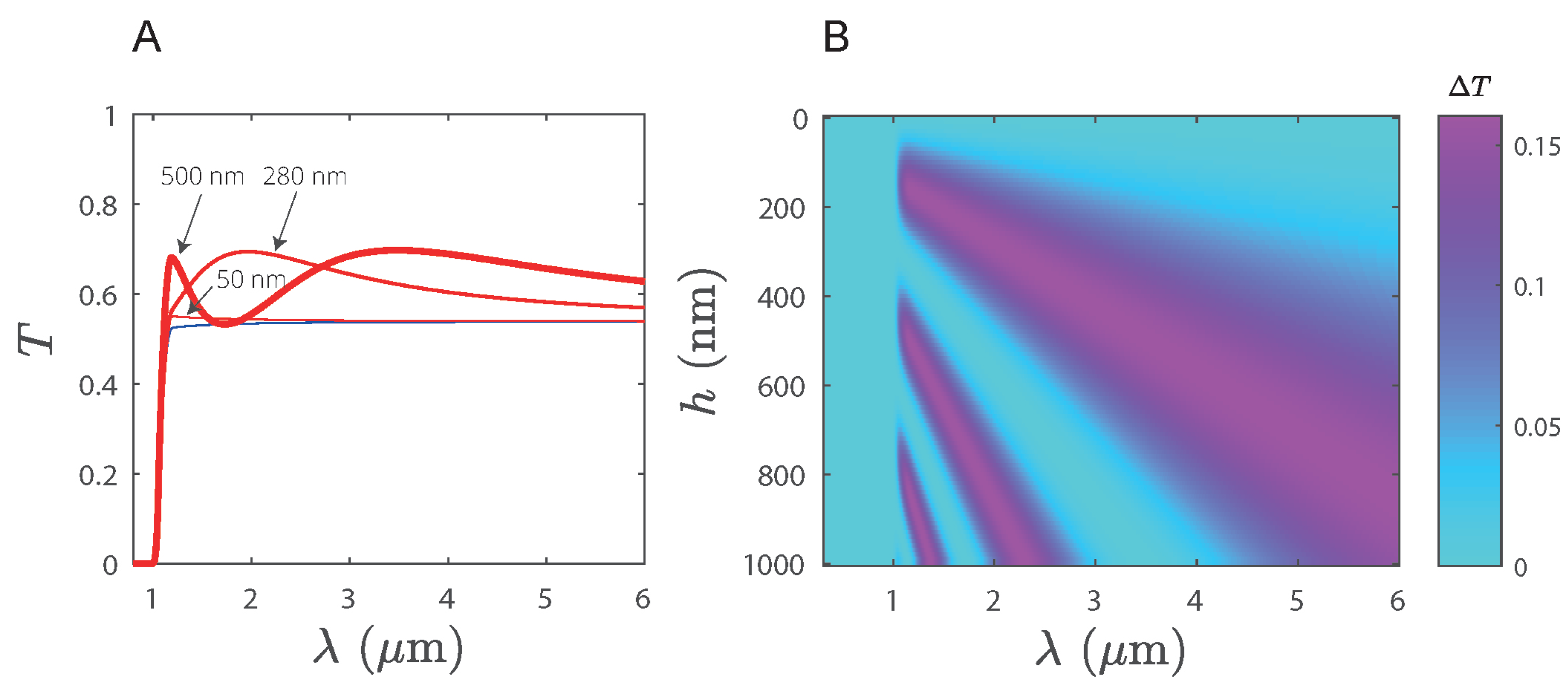
The same type of calculation was performed for transmittance T on double-sided polished silicon substrates in the range of mid-IR, see Figure 11. In part A, a few examples of T against are given for three different coating thicknesses (30, 280, and 500 nm, red curves) and are compared to the transmittance of the bare substrate in blue. Obviously, the silicon substrate is opaque () below some which actually depends on its thickness, here m for a 325 m thick substrate. Above this opacity cut-off, the substrate is basically homogeneously semi-opaque (e.g., at 4 m) while adding a thin coating can dramatically enhance the transmittance. Part B of Figure 11 shows a mapping of the increase of transmittance that the coating provides, namely , against h and . In the mid-IR range, up to 15% of transmittance enhancement can be observed; obviously, this enhancement depends significantly on but can nevertheless be of some interest for monochromatic processes such as imaging.
6. Conclusions
We demonstrated that low-cost, low-tech techniques such as blade coating out of aqueous based dispersions offer an interesting alternative for producing thin, homogeneous, and well controlled nanoporous coatings. While this has been known for years, we demonstrated here the benefit of using dispersions of , an oxide possessing a high refractive index and which results in nanoporous coatings with a high refractive index. These coatings are then interesting candidates for use as an intermediate layer between air and substrates, such as silicon with a even higher refractive index for providing, for instance, anti-reflection features. Eventually, we believe the UV-blocking of the coating could be of potential interest for protecting organic sub-layers and we think the catalytic capabilities of could add even more functionalities to the final material.
Author Contributions
J.L. and L.J.R. conceived the experiments, analysed and modelled the data, and wrote the paper; L.J.R. performed experiments with the help of S.K. and C.P. for mid-IR imaging; L.D.A. provided nanoparticle samples.
Funding
The authors thank funding from Solvay and Agence Nationale de la Recherche (ANR) within the EVAPEC grant 13-BS09-0010-01. The financial support from the CPER CAMPUSB project funded by the French state and the Région Nouvelle-Aquitaine is gratefully acknowledged.
Acknowledgments
The authors thank J.-B. Salmon, Ch. Loussert, M. Lehtihet for fruitful help and support.
Conflicts of Interest
The authors declare no conflict of interest.
Abbreviations
The following abbreviations are used in this manuscript:
| IR | Infra-Red |
| UV | Ultra-Violet |
| SEM | Scanning Electron Microscopy |
| TEM | Transmission Electron Microscopy |
References
- Das, S.; Dowding, J.M.; Klump, K.E.; McGinnis, J.F.; Self, W.; Seal, S. Cerium oxide nanoparticles: Applications and prospects in nanomedicine. Nanomedicine 2013, 8, 1483–1508. [Google Scholar] [CrossRef]
- Younis, A.; Chu, D.; Li, S. Cerium Oxide Nanostructures and their Applications. In Functionalized Nanomaterials; InTech: London, UK, 2016. [Google Scholar] [Green Version]
- Dhall, A.; Self, W. Cerium Oxide Nanoparticles: A Brief Review of Their Synthesis Methods and Biomedical Applications. Antioxidants 2018, 7, 97. [Google Scholar] [CrossRef] [PubMed]
- Prevo, B.G.; Hwang, Y.; Velev, O.D. Convective Assembly of Antireflective Silica Coatings with Controlled Thickness and Refractive Index. Chem. Mater. 2005, 17, 3642–3651. [Google Scholar] [CrossRef]
- Prevo, B.G.; Hon, E.W.; Velev, O.D. Assembly and characterization of colloid-based antireflective coatings on multicrystalline silicon solar cells. J. Mater. Chem. 2007, 17, 791–799. [Google Scholar] [CrossRef]
- Dimitrov, A.S.; Nagayama, K. Continuous Convective Assembling of Fine Particles into Two-Dimensional Arrays on Solid Surfaces. Langmuir 1996, 12, 1303–1311. [Google Scholar] [CrossRef]
- Doumenc, F.; Salmon, J.B.; Guerrier, B. Modeling Flow Coating of Colloidal Dispersions in the Evaporative Regime: Prediction of Deposit Thickness. Langmuir 2016, 32, 13657–13668. [Google Scholar] [CrossRef] [PubMed] [Green Version]
- Loussert, C.; Doumenc, F.; Salmon, J.B.; Nikolayev, V.S.; Guerrier, B. Role of Vapor Mass Transfer in Flow Coating of Colloidal Dispersions in the Evaporative Regime. Langmuir 2017, 33, 14078–14086. [Google Scholar] [CrossRef] [PubMed] [Green Version]
- Joshi, K.; Gilchrist, J.F. Estimation of drying length during particle assembly by convective deposition. J. Colloid Interface Sci. 2017, 496, 222–227. [Google Scholar] [CrossRef] [PubMed] [Green Version]
- Qin, D.; Xia, Y.; Whitesides, G.M. Soft lithography for micro- and nanoscale patterning. Nat. Protoc. 2010, 5, 491–502. [Google Scholar] [CrossRef] [PubMed] [Green Version]
- Gale, B.; Jafek, A.; Lambert, C.; Goenner, B.; Moghimifam, H.; Nze, U.; Kamarapu, S. A Review of Current Methods in Microfluidic Device Fabrication and Future Commercialization Prospects. Inventions 2018, 3, 60. [Google Scholar] [CrossRef]
- Leng, J.; Lonetti, B.; Tabeling, P.; Joanicot, M.; Ajdari, A. Microevaporators for Kinetic Exploration of Phase Diagrams. Phys. Rev. Lett. 2006, 96, 084503. [Google Scholar] [CrossRef] [PubMed] [Green Version]
- Angly, J.; Iazzolino, A.; Salmon, J.B.; Leng, J.; Chandran, S.P.; Ponsinet, V.; Désert, A.; Le Beulze, A.; Mornet, S.; Tréguer-Delapierre, M.; et al. Microfluidic-Induced Growth and Shape-Up of Three-Dimensional Extended Arrays of Densely Packed Nanoparticles. ACS Nano 2013, 7, 6465–6477. [Google Scholar] [CrossRef] [PubMed]
- Kim, E.; Xia, Y.; Whitesides, G.M. Micromolding in Capillaries: Applications in Materials Science. J. Am. Chem. Soc. 1996, 118, 5722–5731. [Google Scholar] [CrossRef]
- Le Berre, M.; Chen, Y.; Baigl, D. From Convective Assembly to Landau Levich Deposition of Multilayered Phospholipid Films of Controlled Thickness. Langmuir 2009, 25, 2554–2557. [Google Scholar] [CrossRef] [PubMed]
- Kumnorkaew, P.; Gilchrist, J.F. Effect of Nanoparticle Concentration on the Convective Deposition of Binary Suspensions. Langmuir 2009, 25, 6070–6075. [Google Scholar] [CrossRef]
- Grosso, D. How to exploit the full potential of the dip-coating process to better control film formation. J. Mater. Chem. 2011, 21, 17033. [Google Scholar] [CrossRef]
- Farcau, C.; Sangeetha, N.M.; Moreira, H.; Viallet, B.; Grisolia, J.; Ciuculescu-Pradines, D.; Ressier, L. High-Sensitivity Strain Gauge Based on a Single Wire of Gold Nanoparticles Fabricated by Stop-and-Go Convective Self-Assembly. ACS Nano 2011, 5, 7137–7143. [Google Scholar] [CrossRef]
- Bodiguel, H.; Doumenc, F.; Guerrier, B. Stick-Slip Patterning at Low Capillary Numbers for an Evaporating Colloidal Suspension. Langmuir 2010, 26, 10758–10763. [Google Scholar] [CrossRef]
- Smith, M.I.; Sharp, J.S. Effects of Substrate Constraint on Crack Pattern Formation in Thin Films of Colloidal Polystyrene Particles. Langmuir 2011, 27, 8009–8017. [Google Scholar] [CrossRef]
- Farr, R.S.; Groot, R.D. Close packing density of polydisperse hard spheres. J. Chem. Phys. 2009, 131, 244104. [Google Scholar] [CrossRef] [Green Version]
- Whitesides, G.M. Self-Assembly at All Scales. Science 2002, 295, 2418–2421. [Google Scholar] [CrossRef] [Green Version]
- Salmon, J.B.; Leng, J. Application of microevaporators to dynamic exploration of the phase diagram. J. Appl. Phys. 2010, 107, 084905. [Google Scholar] [CrossRef] [Green Version]
- Laval, C.; Poulin, P.; Salmon, J.B. Investigation of the dynamics of growth of polymer materials obtained by combined pervaporation and micro-moulding. Soft Matter 2016, 12, 1810–1819. [Google Scholar] [CrossRef]
- Bouchaudy, A.; Salmon, J.B. Drying-induced stresses before solidification in colloidal dispersions: In situ measurements. Soft Matter 2019, 15, 2768–2781. [Google Scholar] [CrossRef]
- Tompkins, H.G.; Irene, E.A. (Eds.) Handbook of Ellipsometry; Springer: Berlin/Heidelberg, Germany, 2005. [Google Scholar]
- Oh, T.S.; Tokpanov, Y.S.; Hao, Y.; Jung, W.; Haile, S.M. Determination of optical and microstructural parameters of ceria films. J. Appl. Phys. 2012, 112, 103535. [Google Scholar] [CrossRef] [Green Version]
- Vangelista, S.; Piagge, R.; Ek, S.; Sarnet, T.; Ghidini, G.; Martella, C.; Lamperti, A. Structural, chemical and optical properties of cerium dioxide film prepared by atomic layer deposition on TiN and Si substrates. Thin Solid Films 2017, 636, 78–84. [Google Scholar] [CrossRef] [Green Version]
- Yvon, H.J. New Amorphous Diserpsion Formula; Technical Report; Horiba Jobin Yvon: France, 2012; Available online: http://www.horiba.com/fileadmin/uploads/Scientific/Downloads/OpticalSchool_CN/TN/ellipsometer/New_Amorphous_Dispersion_Formula.pdf (accessed on 15 June 2019).
- MacLeod, H.A. Antireflection Coatings. In Thin-Film Optical Filters, Fourth Edition; CRC Press: Boca Raton, FL, USA, 2010; pp. 105–184. [Google Scholar]
- Kats, M.A.; Blanchard, R.; Genevet, P.; Capasso, F. Nanometre optical coatings based on strong interference effects in highly absorbing media. Nat. Mater. 2013, 12, 20–24. [Google Scholar] [CrossRef]
- RefractiveIndex.INFO. Optical Constants of Si (Silicon) after Aspnes and Studna, 1983 (n, k for λ = 0.21–0.83 μm). 2019. Available online: https://refractiveindex.info/?shelf=main&book=Si&page=Aspnes (accessed on 4 May 2019).
- Romano, M.; Ndiaye, C.; Duphil, A.; Sommier, A.; Morikawa, J.; Mascetti, J.; Batsale, J.; Servant, L.; Pradere, C. Fast infrared imaging spectroscopy technique (FIIST). Infrared Phys. Technol. 2015, 68, 152–158. [Google Scholar] [CrossRef]
- Kirchner, S.; Narinsamy, S.; Sommier, A.; Romano, M.; Ryu, M.; Morikawa, J.; Leng, J.; Batsale, J.C.; Pradère, C. Calibration Procedure for Attenuation Coefficient Measurements in Highly Opaque Media Using Infrared Focal Plane Array (IRFPA) Spectroscopy. Appl. Spectrosc. 2018, 72, 177–187. [Google Scholar] [CrossRef]
- Dimitrov, A.S.; Nagayama, K. Steady-state unidirectional convective assembling of fine particles into two-dimensional arrays. Chem. Phys. Lett. 1995, 243, 462–468. [Google Scholar] [CrossRef]
- Verneuil, E.; Buguin, A.; Silberzan, P. Permeation-induced flows: Consequences for silicone-based microfluidics. Europhys. Lett. (EPL) 2004, 68, 412–418. [Google Scholar] [CrossRef]
- Randall, G.C.; Doyle, P.S. Permeation-driven flow in poly(dimethylsiloxane) microfluidic devices. Proc. Natl. Acad. Sci. USA 2005, 102, 10813–10818. [Google Scholar] [CrossRef] [PubMed] [Green Version]
- Baron, A.; Iazzolino, A.; Ehrhardt, K.; Salmon, J.B.; Aradian, A.; Kravets, V.; Grigorenko, A.N.; Leng, J.; Le Beulze, A.; Tréguer-Delapierre, M.; et al. Bulk optical metamaterials assembled by microfluidic evaporation. Opt. Mater. Express 2013, 3, 1792. [Google Scholar] [CrossRef]
- Gómez-Graña, S.; Fernández-López, C.; Polavarapu, L.; Salmon, J.B.; Leng, J.; Pastoriza-Santos, I.; Pérez-Juste, J. Gold Nanooctahedra with Tunable Size and Microfluidic-Induced 3D Assembly for Highly Uniform SERS-Active Supercrystals. Chem. Mater. 2015, 27, 8310–8317. [Google Scholar] [CrossRef]
- Gomez-Graña, S.; Le Beulze, A.; Treguer-Delapierre, M.; Mornet, S.; Duguet, E.; Grana, E.; Cloutet, E.; Hadziioannou, G.; Leng, J.; Salmon, J.B.; et al. Hierarchical self-assembly of a bulk metamaterial enables isotropic magnetic permeability at optical frequencies. Mater. Horiz. 2016, 3, 596–601. [Google Scholar] [CrossRef]
Figure 1.
(Left): Thickness of coatings of nanoparticles deposited at different coating speeds v; each point averages at least seven independent experiments. The different morphologies of the sample are zoned at the bottom left for the two systems (blue 4 nm, grey 40 nm) and flat films are obtained otherwise, see Figure 2 top; the dashed lines represent the fitting with a power law. (Right): Rescaled data considering the initial volume fraction and a dry volume fraction . The solid line is a fit according to Equation (3). Inserts: Macroscopic views of the samples highlighting the high degree of transparency.

Figure 2.
(Top): Representative optical microscopy images (bright field) for the coatings deposited at different deposition speeds using sols with nanoparticle size of 4 nm (first row) and 40 nm (second row); the morphologies of the coating are either with thickness oscillations and possible delamination, or flat (see also Figure 1 left). (Bottom): Scanning electron microscopy (SEM) (SEM-FEG HR JEOL 6700F) images of (A) the surface of coatings deposited at different speeds using sols with nanoparticle size of (top) 4 nm and (bottom) 40 nm and (B) of a cross-section of a coating deposited at m.s (40 nm particles).
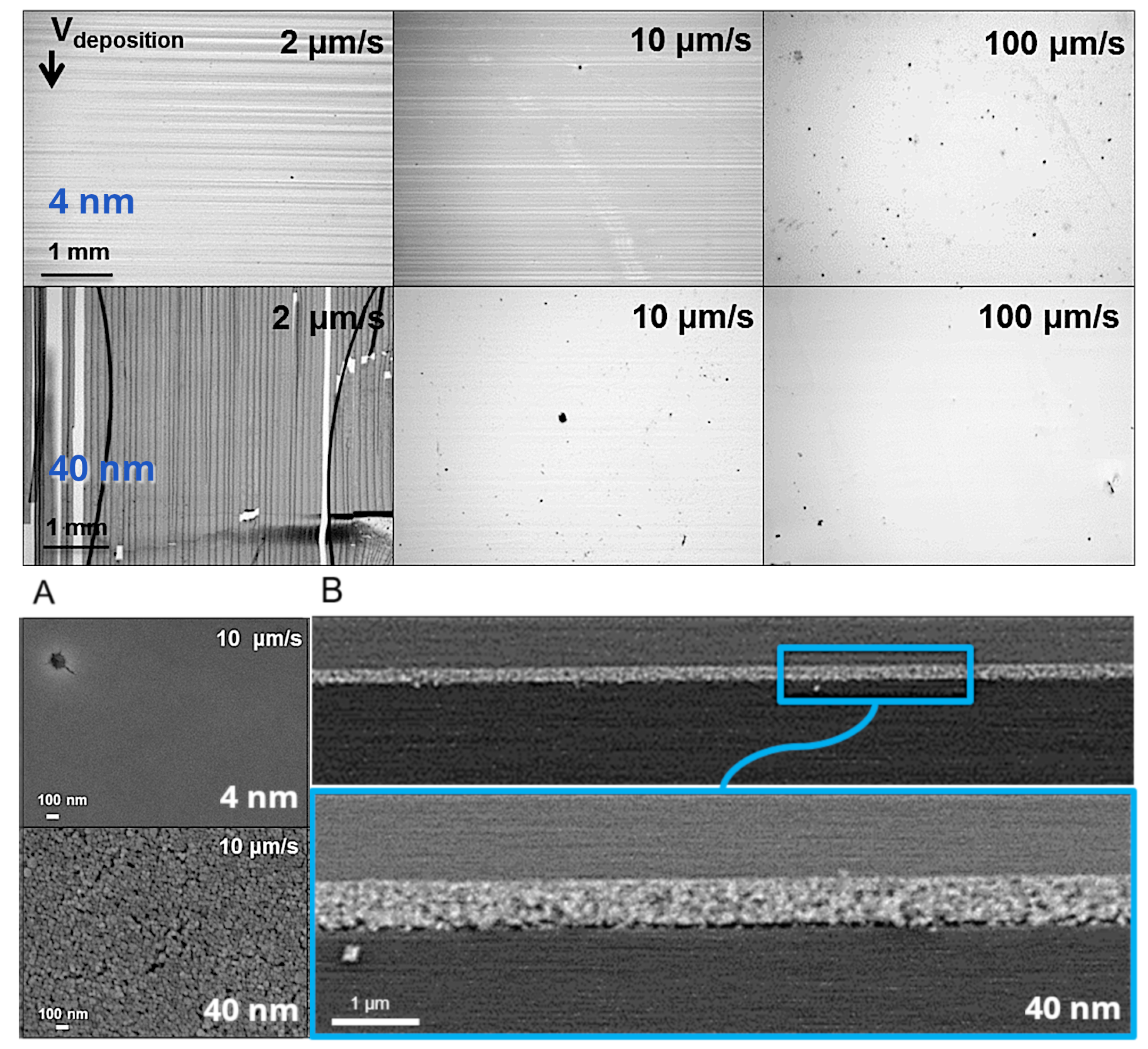
Figure 3.
(A) Materials engineered with -pervaporation made of densely packed nanoparticles, structured with two different designs. In each case, the large figure shows the entire material through a tiled image obtained from optical microscopy in bright field mode and the insert is a SEM view of the top surface of the material. In the upper case, the thickness is about 180 nm; in the bottom case, the thickness is about 260 nm (measured with optical profilometry). (B) Optical microscopy (left) and 3D reconstruction from optical profilometry (right) of the micro-structured materials.
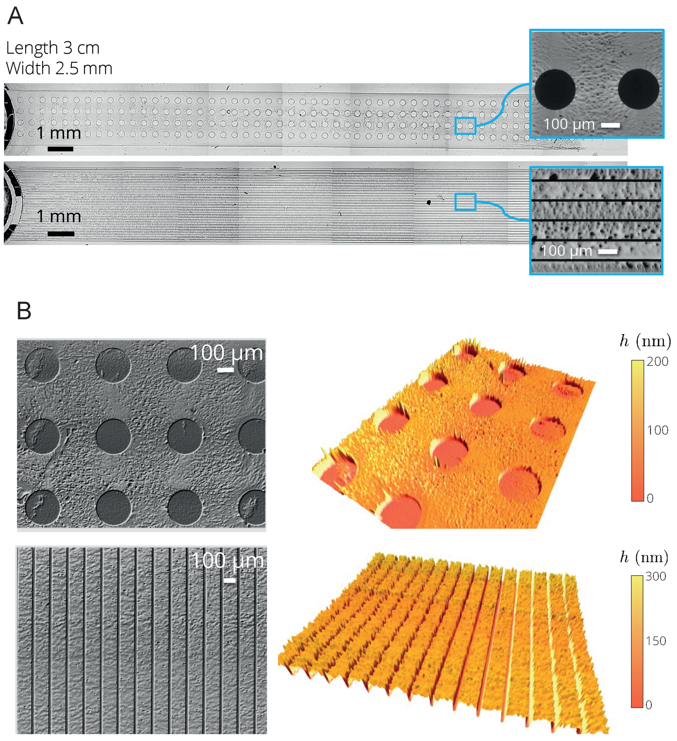
Figure 4.
(Left): Examples of ellipsometric angles and collected for eight angles over a given range of energies (symbols) and best parametrization (solid lines). (Right): Complex refractive index () of a coating obtained out of these ellipsometric measurements.
Figure 4.
(Left): Examples of ellipsometric angles and collected for eight angles over a given range of energies (symbols) and best parametrization (solid lines). (Right): Complex refractive index () of a coating obtained out of these ellipsometric measurements.

Figure 5.
Intensity reflection coefficient R against wavelength for four different coating thickness (values given in red); in red the measurement, in black the calculation according to Equation (1) with no free parameter, in dashed blue the reflection coefficient of a bare silicon substrate. The value of R denoted by the arrow is the best extinction calculated from Equation (1) in the visible to near-infra-red (IR) range.

Figure 6.
(A) Imaging the intensity transmission T at m for a micro-structured pattern. (B) Spectral transmission T in the mid-IR range. Symbols are the local average of the wavelength dependent transmittance for the bare silicon substrate (blue) and for the pattern (red, average along the bright lines). The solid blue line is the theoretical transmission of an incoherent silicon substrate; the solid red line corresponds to a calculated T with a coating thickness nm, whereas the pale red zone shows the parametrization of T with h ranging from 300 to 600 nm.
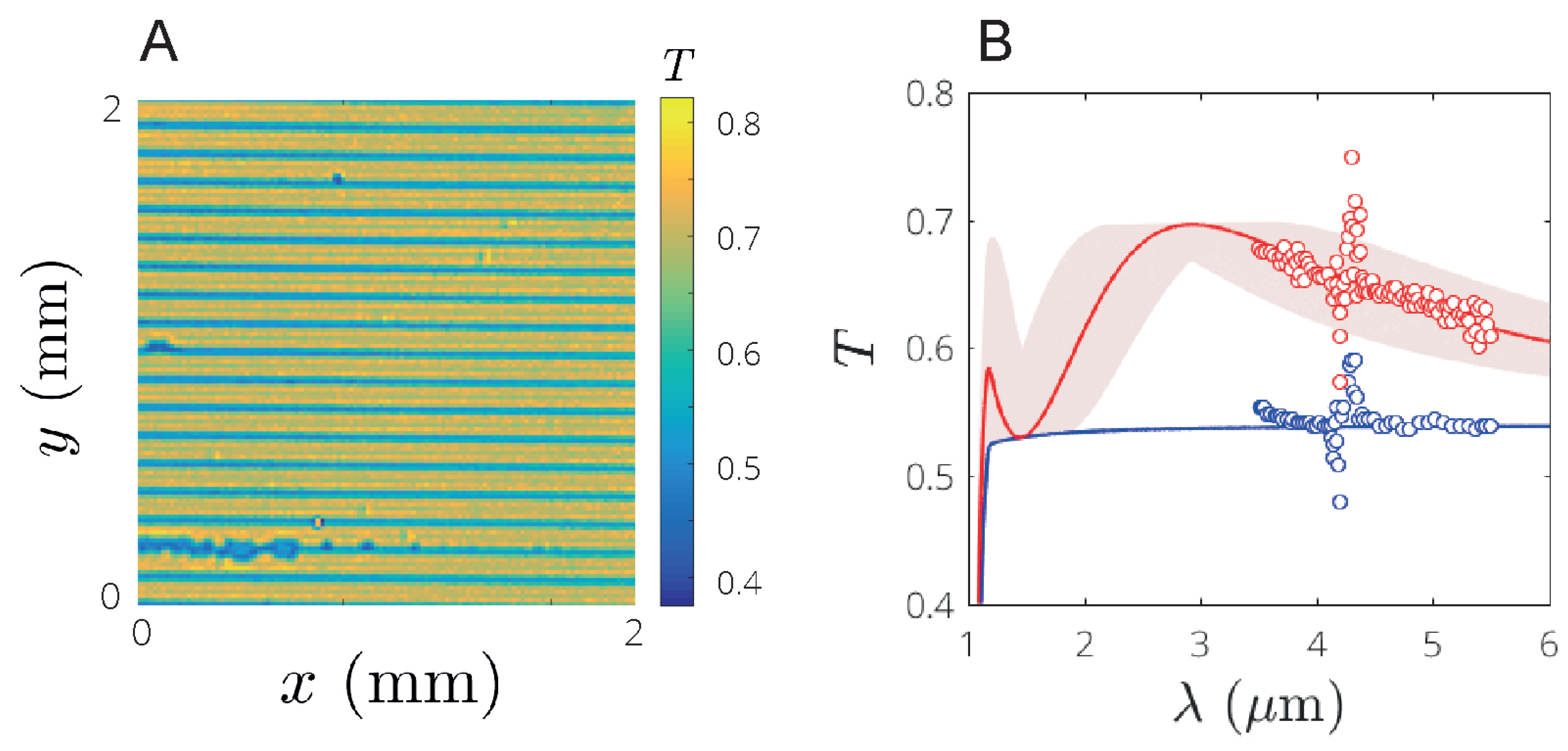
Figure 7.
Transmitted-electron microscopy. (TEM) of nanoparticles deposited on the TEM grid, with diameters in the range of nm (left) and nm (right).
Figure 7.
Transmitted-electron microscopy. (TEM) of nanoparticles deposited on the TEM grid, with diameters in the range of nm (left) and nm (right).

Figure 8.
Sketch of the convective self-assembly (CSA) set-up: (A) A small volume of a dispersion of nanoparticles (the ‘reservoir’, in blue) is placed in-between a static blade and a substrate moving at controlled velocity v. (B) Side view of the geometry which leads to a deposit, in red, of controllable thickness h drying soon at the level of the meniscus [7,8]. The figures were reprinted with permission from Langmuir 2016, 32, 51, 13657–13668. Copyright 2016 American Chemical Society.

Figure 9.
Sketch of the -pervaporation technique leading to micro-structured deposits: A poly(dimethyl siloxane) (PDMS) mould (left) is designed with channels initially filled with a dilute dispersion; solvent spontaneously permeates across the elastomer, concentrates the nanoparticles, and leads to a solid material out of the dispersion upon removal of the mould (right).
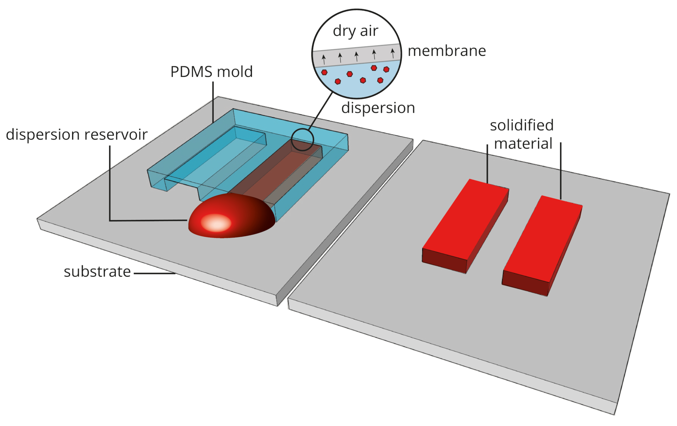
Figure 10.
Reflectance R calculated for a nanoporous coatings of variable thickness h deposited on a silicon substrate. (A): Small thickness h in the visible and near-IR range; (B): Large thickness in the mid-IR range.
Figure 10.
Reflectance R calculated for a nanoporous coatings of variable thickness h deposited on a silicon substrate. (A): Small thickness h in the visible and near-IR range; (B): Large thickness in the mid-IR range.
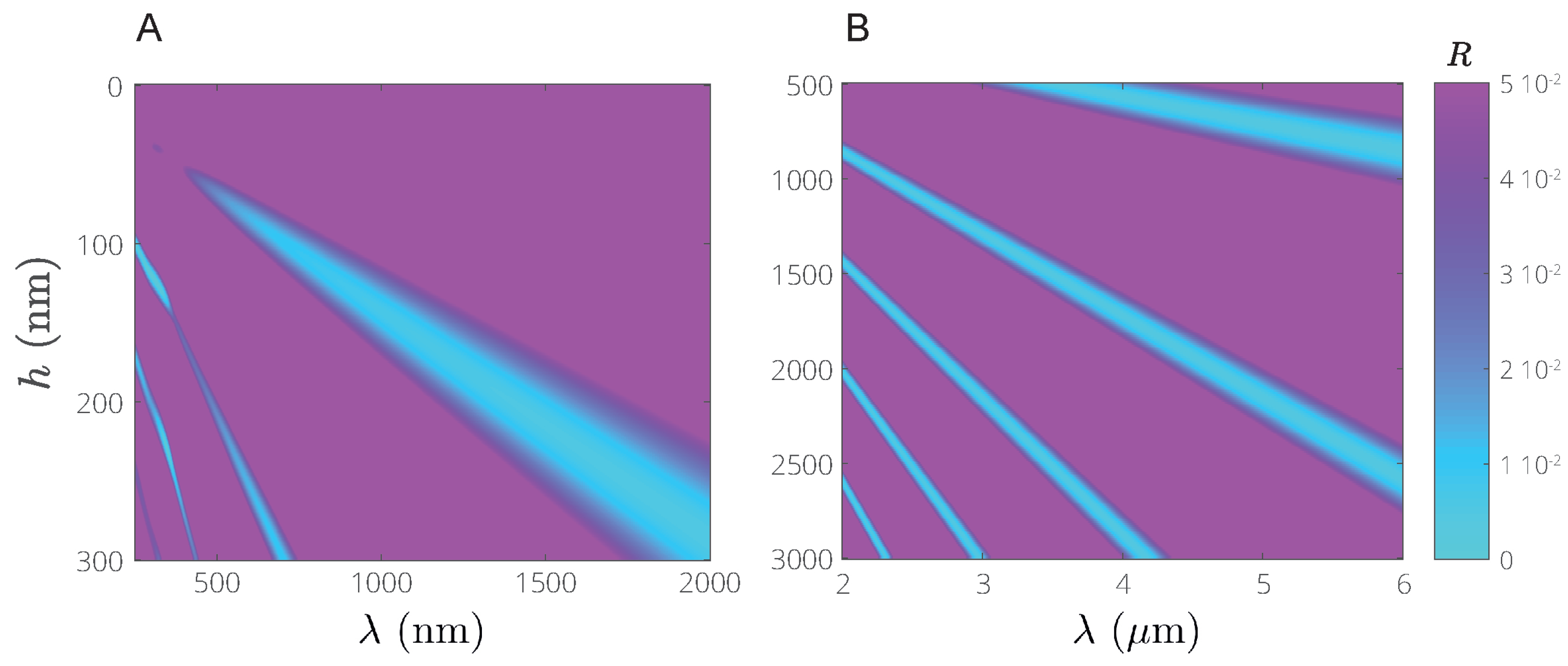
Figure 11.
(A): Transmittance T calculated for a nanoporous coatings of variable thickness h (red curves) deposited on a silicon substrate (blue curve). (B): Transmittance excess as a function of wavelength and coating thickness h.
Figure 11.
(A): Transmittance T calculated for a nanoporous coatings of variable thickness h (red curves) deposited on a silicon substrate (blue curve). (B): Transmittance excess as a function of wavelength and coating thickness h.
© 2019 by the authors. Licensee MDPI, Basel, Switzerland. This article is an open access article distributed under the terms and conditions of the Creative Commons Attribution (CC BY) license (http://creativecommons.org/licenses/by/4.0/).
Share and Cite
MDPI and ACS Style
Romasanta, L.J.; D’Alençon, L.; Kirchner, S.; Pradère, C.; Leng, J. Thin Coatings of Cerium Oxide Nanoparticles with Anti-Reflective Properties. Appl. Sci. 2019, 9, 3886. https://doi.org/10.3390/app9183886
AMA Style
Romasanta LJ, D’Alençon L, Kirchner S, Pradère C, Leng J. Thin Coatings of Cerium Oxide Nanoparticles with Anti-Reflective Properties. Applied Sciences. 2019; 9(18):3886. https://doi.org/10.3390/app9183886
Chicago/Turabian StyleRomasanta, Laura J., Lauriane D’Alençon, Sara Kirchner, Christophe Pradère, and Jacques Leng. 2019. "Thin Coatings of Cerium Oxide Nanoparticles with Anti-Reflective Properties" Applied Sciences 9, no. 18: 3886. https://doi.org/10.3390/app9183886
Note that from the first issue of 2016, this journal uses article numbers instead of page numbers. See further details here.