A Novel Modular Multiport Converter for Enhancing the Performance of Photovoltaic-Battery Based Power Systems


1
Department of Electrical and Electronic Engineering, University of Nottingham, Nottingham NG7 2RD, UK
2
National Authority for Remote Sensing and Space Sciences, Cairo 1564 (Alf Maskan), Egypt
*
Authors to whom correspondence should be addressed.
Appl. Sci. 2019, 9(19), 3948; https://doi.org/10.3390/app9193948
Submission received: 24 July 2019
/
Revised: 9 September 2019
/
Accepted: 16 September 2019
/
Published: 20 September 2019
(This article belongs to the Special Issue Smart PV Generation with Energy Storage)
Abstract
:This paper introduces a novel multiport power converter with modular architecture for photovoltaic (PV)-battery based power systems. Compared to conventional centralized multiport converters, the proposed converter significantly improves the utilization of PV available energy and battery capacity as it does not require a high number of series-connected PV and battery modules. The proposed converter also eliminates the need for additional battery cell/module equalizer circuitry by being able to implement directly energy management strategies that consider the different capabilities of battery modules to ensure charge/stress balancing. This makes it a promising solution for interfacing second-life batteries or for systems that utilize batteries with a high degree of mismatch. The modularity of the proposed converter enhances system reliability and fault tolerance and reduces the power/voltage ratings of the power electronic devices. The converter modes of operation, control strategy and design considerations are discussed. A 75 V/1 kW integrated PV-battery power system prototype is built and tested to validate the concept.
1. Introduction
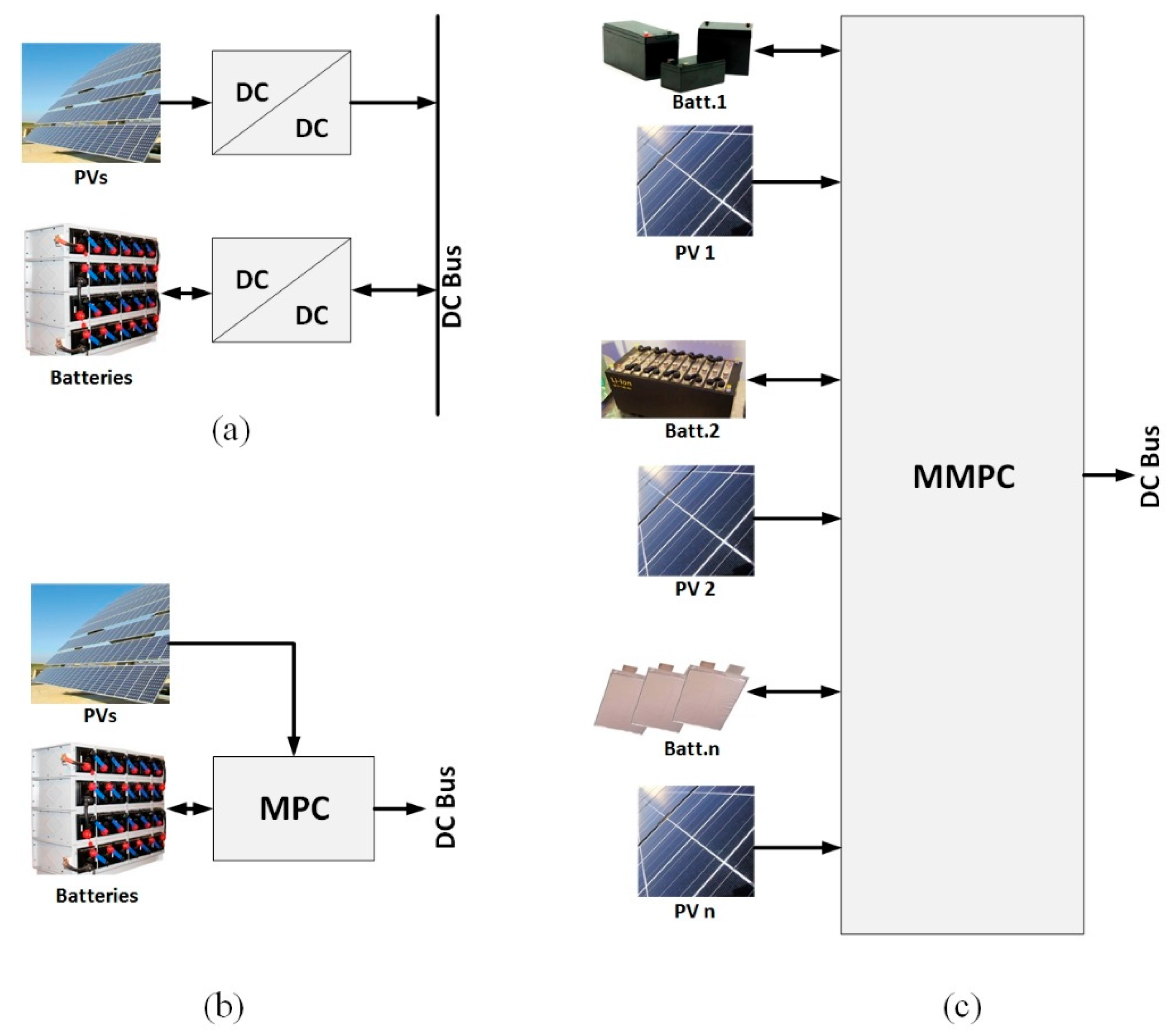
The need to further advance the development of renewable energy sources points to exploring new ways of implementing power systems for new stationary and mobile applications and integration with energy storage. The conventional structure of DC power systems with renewable sources were constructed such that each source interfaces to the power bus via its own DC-DC converter which controls its mode of operation and adapts its voltage level with the bus voltage. One of the most common examples for such a structure are the stand-alone photovoltaic (PV) power systems which consists of two DC-DC converters: one is unidirectional for PV maximum power point tracking (MPPT) and the other one is bidirectional to control battery charge/discharge operations [1,2,3,4] as seen in Figure 1a. Recently, multiport converter (MPC) topologies have been shown to provide advantages compared to the convention systems, including lower cost and higher power density.
The MPC topology can be fully isolated implementing multi-winding transformers with half-bridge topology [5] or full-bridge topology [6,7,8] to allow full isolation between all ports. Other alternatives are partially isolated [9,10,11,12,13,14] or non-isolated topologies [15,16,17,18,19,20,21,22]. The isolated and partly isolated MPCs are better choices for applications that require some sort of galvanic isolation, however the use of transformer may reduce the power density of such converters. On the other hand the non-isolated MPCs can have simpler control design and better efficiency [23] but with limited voltage mismatch level between sources and the power bus.
The structure of most of these MPCs are centralized topologies, built based on a central converter that interfaces different power sources and energy storage with the power bus as seen in Figure 1b .The problem with these centralized multiport converters (CMPCs), when a PV-battery system is considered, is that they require strings of a high number of series-connected PV-panels in order to be able to interface to high voltage power buses to minimize converter current rating but this leads to several disadvantages. The most important one is the severe reduction in the throughput power when one or several panels are subject to a partial shading or partial shading-like characteristics due to panel irregularities as investigated in References [24,25,26,27]. Additionally, all the PV-panels within the string must be at the same orientation in order to achieve identical light incident angles and balanced power for all panels within the string. This limits the degree of freedom for mounting the PV-panels which needs to be maximized, especially for the household applications due to the limited availability of space.
Similarly, a CMPCs with a higher voltage power bus also requires battery strings with a high number of series-connected battery cells which have several disadvantages related to the need for additional complex charge balancing circuitry and limited utilization of the available capacity of the battery as investigated in References [28,29,30,31,32]. Additionally, the CMPCs are not fault tolerant as a single failure within the converter will cause the overall system to be unusable.
The modular structure of the MPCs shown in Figure 1c can improve system flexibility and fault tolerance as presented in Reference [33], where the structure of a power system based on parallel MPCs has been investigated. However, it kept the centralized structure of PV/battery strings that needs a high number of series-connected PV/battery cells for interfacing to a higher voltage power buses. Other topology for the modular structure of the MPC has been proposed in Reference [34] that implements a sub-modules of a fully isolated MPC as a building block for the modular converter to enable decentralized PV/battery strings. However, it requires a large number of semiconductor switches/diodes per each sub-module that causes the power converter to be very complex.
In this paper, a new multiport converter topology for interfacing PVs and batteries has been developed. The developed topology has been used as a sub-module to build a new modular multiport converter (MMPC) which removes the need for high voltage strings of PV/batteries with their related problems. It also reduces the power rating and voltage stress of the power electronics that may enhance the overall system efficiency. One of the most important merits of the propose topology is that it can perform battery charge balancing for a wide range of battery module imbalances. This is of particular interest when employing second-life batteries (SLB) which are receiving considerable attention [35,36,37].
The paper is organised as follows: the system level analysis of the proposed converter is presented in Section 2; the topology of the scalable power module design is discussed in Section 3; then, operation of the proposed converter is discussed in Section 4 and experimental results to verify the operation of the converter is presented in Section 5; finally, Section 6 concludes the main points of this paper.
2. System Level Analysis of Proposed Converter
The proposed MMPC utilizes a number low power MPC modules, each MPC module (referred to as power module (PM)) has as inputs a PV port and a battery port. The output of the modules, which can accommodate different ratings for PV/batteries, are connected in series to provide the full bus voltage/power as shown in Figure 2.
2.1. Converter Global Control
The global controller should ensure the regulation of the bus voltage at desired value and manage the power sharing among the PMs according to the available power from the different PV modules as well as the state of charge (SoC)/state of health (SoH) of the battery modules. This is to ensure maximum power extraction from all the PVs as well as charge/stress balancing among all the battery modules.
The power sharing of the individual PMs is controlled through controlling the ratio of output voltage that each PM contributes, to the fulfillment of required bus voltage (Vbus):
where Pbus is the bus power, Ibus is the bus current, n is number of PMs, Pi is the power contribution of the ith PM and Vi is its output voltage which estimated as:
where Ppvi is the power of the PV-module of the ith PM and Ki is a sharing factor defined based on the SoC of the module’s battery and estimated as:
The global controller then forwards the module’s share of the bus voltage Vi as a reference voltage to the module’s local output voltage controller.
During time periods when the PV power exceeds the load and the batteries should be in charging mode, the PMs which interface to the battery modules with lower SoCs should contribute less to the bus voltage/power (smaller Vi) to allow more PV power to be used for charging their battery modules. On the other hand, PMs which interface to the battery modules with higher SoCs contributes higher voltage/power to the bus to maintain the required bus voltage. As a result, a lower PV power will be directed from their PV modules to their battery modules for slower charging.
During the time periods when the PV power is lower that the load, the battery modules will be in discharging mode to supply the load power. PMs which interface to battery modules with lower SoCs should contributes less to the bus voltage/power to allow slower discharging while PMs which interface to battery modules with higher SoCs should contribute more to the bus voltage/power to compensate, and this will mean faster discharging and reduction of the SoCs imbalances. Through this strategy, charge balancing can be achieved among battery modules that may be at different SoCs due to batteries capacity mismatching. Balancing of thermal stress among battery modules under mismatched equivalent series resistances (ESR) in the battery cells [30] (which can be significant if there are peak charge/discharge power of the battery) can also be achieved by adapting the energy management strategy accordingly; however, this will not be considered further within this paper.
2.2. Balancing Range
As the charge balancing among the battery modules is controlled by the different voltage share among the PMs as previously described, the range of output voltage for the PMs determines the range of imbalance in battery modules SoC that can be handled by the MMPC.
The voltage contribution of the PM which interfaces to the battery module at lowest SoC is defined as:
where Kmin is the sharing factor of the PM that interface to the battery module with the lowest SoC.
In order to keep the bus voltage at the reference value unaffected by the balancing process, the sharing factor of the PM which interfaces to the highest SoC battery module (Kmax) should satisfy:
Based on Equation (4), Kmin can be estimated based on the minimum achievable output voltage which is limited by the voltage of the PV-module at maximum power point (Vmpp) during sunlight. The voltage share of the PM that interfaces to the battery with the highest SoC (Vmax) should satisfy Equation (6) in order to maintain the bus voltage at the same level.
It can be observed from Equations (4) and (6) that, the wider the output voltage range of the PM, the bigger the disparity in battery SoC that can be handled. Accordingly, the topology of the MPC used for the PMs affects the operating range and SoC balancing as will be investigated in Section 3.
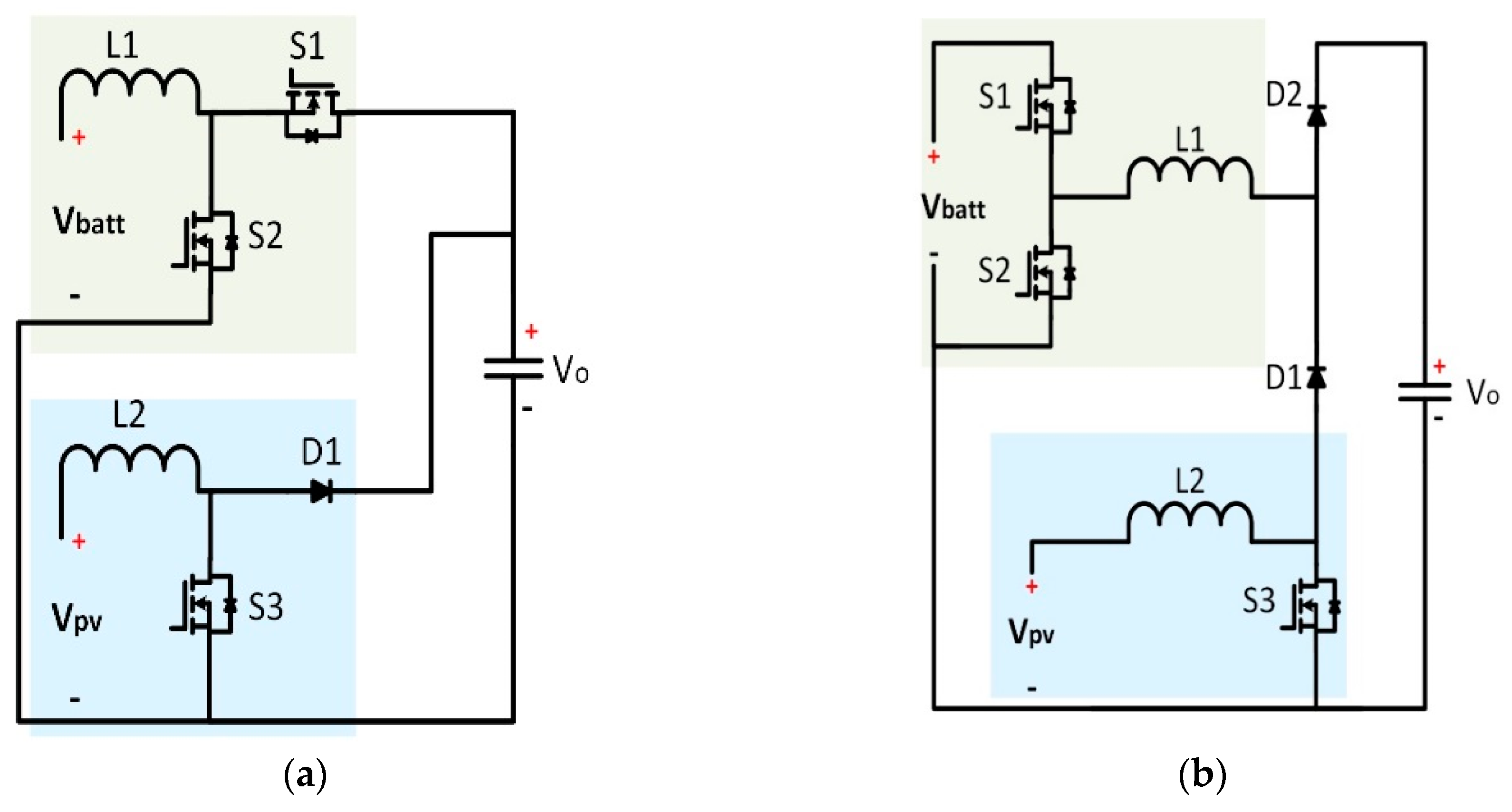
3. Converter Topology for the Power Modules
Non-isolated MPCs are usually built based on combinations of basic pulse width modulation (PWM) DC-DC converters (buck, boost or buck-boost) or based on a reduced form of the combined converter [15]. The most common topology for MPCs is the boost-boost topology (Figure 3a) which uses multiple boost converters to interface the different power sources to the power bus. However, this topology has some limitations if implemented in the proposed MMPC. The minimum output voltage of the PM based on this topology is limited to the battery voltage while the maximum output voltage is determined by the boost ratio of the PV-converter during the availability of PV power, and the battery converter when PV power is unavailable. If the maximum voltages for battery and PV are designed to be equal at a value of Vpv, then the minimum achievable output voltage under this condition is Vpv, while the maximum achievable output voltage will be more than Vpv depending on the boost ratio of the converters. Accordingly, if a boost ratio of two is considered (although feasible, this may affect efficiency), the operating voltage range of the converter will be from Vpv up to 2 Vpv.
The proposed topology for the MPC cell shown in Figure 3b has been developed based on the integration of a boost stage which interfaces to the PV-module and a buck stage which interfaces to the battery module. This topology enables a dual step-down and step-up voltage conversion for the battery voltage providing more flexibility for the choice of battery voltage. To achieve this, blocking diodes D1 and D2 are needed to decouple the PV boost from battery converter in order to extend power flow controllability of the developed MPC. To better analyze the operations of the proposed converter, the three different operating modes will be further analyzed under continuous conduction mode (CCM) neglecting the diode forward voltages.
3.1. Single Input Double Output Mode
For the single input double output (SIDO) mode, the PV-module provides the power for the load and battery charging which means for all modes described below, the current in L1 will flow towards the battery. In this mode, the operating modes of the converter which are illustrated in Figure 4, are as follows:
- Stage I is illustrated in Figure 4a: switch S3 is turned ON which means the power extracted from the PV will be used to increase the energy stored in L2 i.e., the voltage across inductor L2 is VPV; due to the initial negative current in L1, diode D1 will have to be turned on and if switch S2 is OFF, S1 is conducting through its body diode, the voltage across inductor L1 is (−Vbatt) which will cause its current to reduce in amplitude.
- Stage II is illustrated in Figure 4b: switch S3 is turned OFF while switch S2 is still OFF and S1 is conducting through its body diode. The difference between the currents in inductors L1 and L2 will flow to the output via D2 which means the voltage potential at the common point between L1 and L2 is clamped to Vo. Therefore, the voltage across inductor L1 is (VO−Vbatt) and the voltage across inductor L2 is (VPV−VO).
- Stage III is illustrated in Figure 4c: switch S3 is OFF while switch S2 is ON and S1 is OFF. This has the following implications: the battery is disconnected (ib = 0), the voltage across the inductor L1 is VO, therefore the current in L1 increases in amplitude and the current in L2 continue to decrease as the voltage across the inductor L2 remains (VPV−VO).
Figure 5 shows the typical waveforms of the converter during SIDO mode. By applying the voltage balance principle to the inductor L2, the following equations can be obtained:
Therefore,
where d3 is the duty ratio of switch S3, VPV is the PV-module’s voltage and VO is the converter output voltage.
Similarly, by applying the voltage balance principle to inductor L1, the following equations can be obtained:
Therefore, the relationship between the battery and output voltages and switches duty cycles defined as:
where d2 is the duty ratio of switch S2; as the switches S2 and S1 operate complementary, (10) can be reconstructed as:
where d1 is the duty cycle of the switch S1. Based on (8), d3 controls the PV current and therefore the maximum power point operation of the PV-module independent of the output voltage (as long as it is larger than PV voltage), while d1 controls the output voltage based on Equation (11) for a defined d3 and an actual value of battery voltage Vbatt.
3.2. Double Input Single Output (DISO) Mode
The converter operates in double input single output (DISO) mode when the load demand exceeds the power capability of the PV-module. Therefore, the extra power is supplied by the battery module which means that the current in L1 is negative (opposite to the direction indicated by the arrow). For this mode, the operating modes of the converter are as:
- Stage I is illustrated in Figure 6a: switches S3 and S1 are turned ON and switch S2 is OFF which means that the PV is shorted via L2 forcing the diode D1 to be reverse biased (OFF) and only the battery provides current to the load. This means that the voltage across inductor L1 is negative (VO−Vbatt) and its current raises and the voltage across inductor L2 is (+VPV) forcing its current to increase.
- Stage II is illustrated in Figure 6b: switch S3 is turned OFF while switch S1 is still in conduction. This means the PV will contribute current towards the load and the diode D1 will conduct. Therefore, the voltage across inductor L1 remains (VO−Vbatt) and the voltage across inductor L2 is (VPV−VO) forcing its current to decrease.
- Stage III is illustrated in Figure 6c: switches S1 and S3 are turned OFF while switch S2 is conducting through its body diode. Therefore, the voltage across inductor L1 is (VO) causing the amplitude of its current to decrease. The voltage across inductor L2 remains negative (VPV−VO) and it current continues to decrease.
Figure 7 shows the typical waveforms of the converter during DISO mode. As can be observed, the operation of the PV-converter remained unchanged and consequently it is governed by Equation (8). For the battery converter, applying the voltage balance principle to inductor L1, the following equations can be obtained:
Therefore,
3.3. Single Input Single Output Mode
The converter is able to work in single input single output (SISO) mode when there is no power available from the PV-module (shading condition), therefore all the load power has to be supplied by the battery module. As the PV-converter is not in operation, the proposed converter operation during this mode is determined by the battery converter which operates as a normal buck converter and its output voltage is determined by Equation (13) in the same way as for DISO mode.
As can be observed from analyzing the different modes of operation, the proposed converter output voltage range is determined by the mode of operation as follows:
During SIDO mode which covers the charging of the battery from the PV: based on Equation (11) the proposed converter works in buck-boost operation therefore the theoretical output voltage ranges from 0 V to voltages higher than the battery voltage (Vbatt).
During DISO and SISO modes which only cover the discharge of the battery, based on Equation (13), the theoretical output voltage ranges from 0 V up to Vbatt (i.e., the output voltage needs to be smaller than the battery voltage).
Accordingly, and in order to ensure the proper operation of the proposed converter under all modes of operation, the voltage of the battery module should be selected such that: the minimum voltage of the battery module (at minimum SoC) should be higher than the maximum targeted output voltage. On the other hand, in order to ensure continuous extraction of maximum power available from the PV modules, the voltage of the PV-module should be selected such that: the maximum voltage of the PV-module should be lower than the minimum targeted output voltage. This will be discussed in more details in Section 4.
4. Operation of the Proposed MMPC
4.1. Operation Control
The main objectives of the control scheme of the proposed MMPC is to maintain the bus voltage at its desired value while ensuring corrective measures are taken to address the imbalance in the SoC of the batteries and/or available PV power among the PMs. To achieve this, a global controller (shown in Figure 8) has been proposed to determine the power contribution of each PM. It uses a weighting factor (Ki) calculated according to Equations (1)–(3) and also considers the maximum power available from the PVs of all PMs. These are used to calculate PM’s output voltage references Vi_Ref accordingly. These are then passed to the local PM control loops which control the duty cycles of the switch Si3 (di3) and the switch Si1 (di1) in order to achieve the reference output voltage as can be seen in Figure 9. During the charging process of the battery module, based on the maximum possible charging power of PM’s battery, each PM local controller determines the operating mode of its PV-converter (MPPT) either to work at or away from MPP in order achieve the module’s reference output voltage requested by the global controller. The MPPT algorithm at the local control loop of the PM controls the current and accordingly the power of the PV-module through the duty cycle of the switch S3 (d3) independent of the output voltage (as long as it is larger than PV-module voltage), while the duty cycle of the switch S1 (d1) controls the output voltage of the power module based on Equation (11) for a defined d3 (defined by the MPPT) and an actual value of battery voltage Vbatt.
Information about state of charge and state of health of the individual battery cells within the battery modules gathered by the battery management system (BMS) can be used to determine the charge/discharge power of each battery module at global control loop. The proposed converter reduced the required number of series-connected battery cells through the decentralized battery modules which can eliminate the need for cells balancing/equalization circuits as investigated in Reference [38]. If a fault in any one of the PMs prevents it delivering its desired power contribution to the bus, this imbalance will cause its output voltage to drop down to zero, causing the forward bias and therefore conduction of the diodes D1 and D2 as well as the anti-parallel (body) diode of S3 (that can be easily duplicated to grantee fault tolerance operation). This means there will be a natural bypassing of the faulty modules. Losing the voltage contribution of this faulty module will be detected by the global controller which will then modify the reference voltage of the remaining PMs in order to compensate for that fault and maintain the bus voltage at its reference value. These measures can provide a wide range of fault tolerance for the proposed power system: this is one of the important advantages of the proposed MMPC.
4.2. Converter Design Analysis
The selection of the voltages for the battery and PV modules which interface to the PM is one of the most important design parameters for the proposed MMPC as it determines the imbalance range that can be handled between the PM’s batteries. During battery charging, if for a given PM the PV boost is operating at its MPP, then the minimum achievable output voltage for this PM is Vpv-max which is PM’s PV-module voltage at MPP.
During battery charge/discharge (battery buck/boost), the maximum achievable output voltage of the PM is the voltage of its battery (Vbatt). As a result, the maximum imbalance in the SoCs of the PMs’ batteries that can be handled can be derived based on Equations (4) and (6) under these conditions as:
As can be observed from Equation (14), the wider the range between battery voltage and PV-module voltage at MPP, the wider the imbalance among the PMs’ batteries that can be handled.
Determining the number of PMs is also one of the key design parameters of the proposed MMPC, as it defines the maximum utilization of the battery modules as well as the PV modules’ available power. For a defined output voltage level for the proposed MMPC, increasing the number of PMs results in reducing the required terminal voltage of a single battery module which in turn reduces the number of series-connected battery cells per module and consequently better utilization of available battery capacity.
The power extracted from a single PV-string is limited by the weakest PV-module in the string, this weakness being due to aging/degradation or shadowing. Segmenting the single PV-string into several PV-modules interfacing the different ports of the proposed converter will improve the utilization of the available power as it allows independent MPPT for each PV-module limiting the effect of weak PV-modules on the overall performance of the PV-string. This also gives flexibility in configuring PV-modules with different angles/orientations which enhances the utilization of the space available for mounting PV-modules.
Increasing the number of PMs also decreases the voltage stress of the switches which enables the use of low voltage rating devices with smaller parasitic resistances and capacitances which may reduce the conduction and switching losses of the switches and boosts the system efficiency.
Increasing the number of modules increases the fault tolerance of the MMPC as it decreases the impact of the faulty module on the overall system operation.
On the other hand, increasing the number of PMs results in increased converter complexity due to the increased number of local control loops which require dedicated measurements and their own PWM. Therefore, the selection of the number of modules for a particular application needs to be the subject of a tradeoff study where the impact on system efficiency, complexity and cost is evaluated against improving the maximum utilization of battery capacity and available PV power and the fault tolerance of the system.
Since the proposed converter is aimed to operate with very high switching frequency in order to achieve high power density, current ripple of the PV-stage inductor (L2) of the PMs that may affect the efficiency of the MPPT for the PV modules will be in very high frequency and hence a proper decoupling capacitor can be implemented at the PV-stage input.
5. Experimental Results
In order to validate the proposed MMPC, an experimental prototype has been developed that is able to deliver 1 kW of power at a bus voltage of 75 V. The experimental prototype shown in Figure 10 consists of three PMs (M1, M2 and M3) built based on the proposed topology discussed in Section 3 with specifications shown in Table 1.
Each PM interfaces with a programmable power supply that emulates a PV-module. Three lead acid battery modules have been used to provide energy storage capability for each module. The digital control platform consists of a powerful floating point digital signal processor (DSP) (Texas Instruments TMS320C6713) mounted on a commercial kit board that runs all the complex calculations required by the control, and a custom field-programmable gate array (FPGA) platform built around the (ProASIC®3) chip that is controlling the A/D feedback signal acquisition and the generation of the PWM signals.
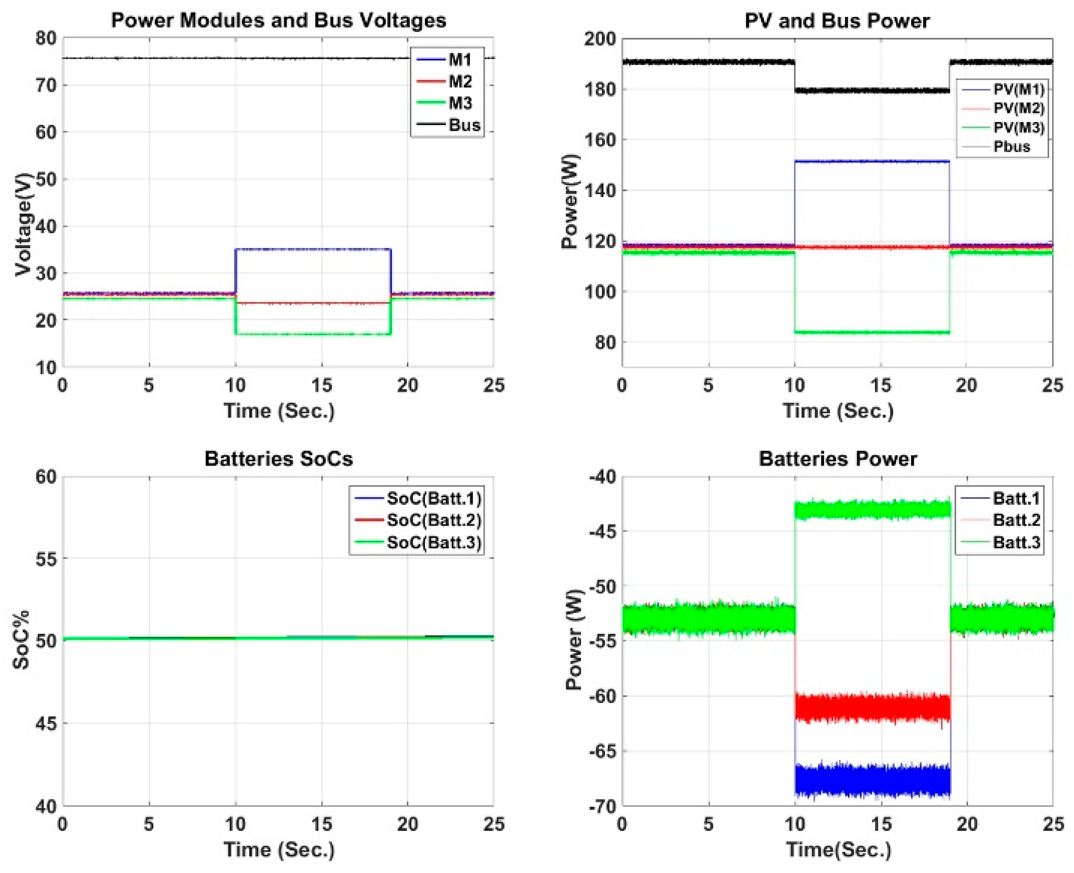
The evaluation of the proposed MMPC and associated management algorithms was achieved in four tests. Test 1, which is shown in Figure 11, was made for battery charging and assumed balanced batteries (i.e., the three battery modules had the same SoC). Initially the three PV-sources provided nearly equal power (around 117 W each) which resulted in an equal voltage contribution (around 25 V) for all the PMs to the MMPC bus voltage (75 V) and also in maintaining balanced charging powers (3 × 55 W) for the battery modules. At t = 10 s, a disturbance had been introduced to the system by slightly reducing the load power by 5% as well as imposing an imbalance in the PV powers (Ppv1 = 150 W; Ppv2 = 117 W; Ppv3 = 85 W). Accordingly, if the module voltage contributions were kept the same, the imbalance in PV powers would cause a direct imbalance in the charging powers of the battery modules which in turn would lead to significant SoC imbalances. In order to minimize this, the proposed management algorithm allowed the modules to contribute with imbalanced voltage/power to the bus voltage/load power in order to minimize the battery power imbalance which ultimately would provide minimum SoC imbalance. This was seen during the time (10 < t < 19 s), where the voltage contribution of M1 with highest PV power had been increased from 25 V to 35 V to direct most of the increased PV power (117 W→152 W = +30%) to the bus/load. On the other hand, the voltage contribution of M3 with lowest PV available power (120 W→85 W = −30%) had been decreased to 17 V (this is the minimum possible, equal to the PV voltage) to minimize the module power contribution to the bus, allowing for more power to charge the battery module (53 W→42 W = −20% instead of 37 W). These imbalances in the voltage contributions of PMs was nearly compensating for the PV power imbalances, limiting the buildup of battery SoC divergence. Throughout the whole test, it can be seen that the control was able to maintain the bus voltage at 75 V under all conditions, unaffected by the PV imbalance.
The second test, shown in Figure 12, evaluated the capability of the MMPC to maintain the bus voltage as well as balanced SoCs for the battery modules under the presence/absence of PVs power. Initially (t < 10 s), the power of all the PV-sources were almost the same (=118 W) and all batteries were charging with the same power (=44 W) to maintain balanced SoCs. At t = 10 s the PV-source of M3 was switched OFF. This forced the battery of M3 to switch from charging to discharging state in order to contribute power to the load requirement, which needs to be kept at a minimum in order to limit the divergence of the battery module SoC. Therefore, the voltage contribution of M3 was set to the minimum (17 V). To compensate for this, the voltage contributions of M1 and M2 were increased delivering more power to the bus/load and less power (44 W ↓30 W) to charge their batteries but keeping the bus voltage at the reference level (75 V although a small dip is visible). When another PV-source (PV1) is switched OFF (t = 12.5 s), the voltage contribution of M2 increases to the maximum (36 V) to maximize its power share to the load and minimize the charging power of its battery module (30 W ↓9 W), allowing the modules without their PV source (M1 and M3) to minimize their power contribution to the load. The last PV-source (PV2) to be switched off was M2 at t = 16 s which means all the three battery modules were discharging, therefore the voltage/power contributions of all the modules were the same, to have same discharge power and maintain balanced SoCs. The second part of this test consisted of switching ON the PV sources in the same order. It can be seen that the voltage contribution of each module changes in a similar way as in the previous steps, which is consistent with the aim of minimizing as much as possible the power imbalance of the batteries while delivering a constant bus voltage to the load.
The third test, shown in Figure 13, evaluated the capability of the MMPC to reduce the charge imbalance of the battery modules. As it required a long time to obtain a noticeable change in the SoC of the battery modules when using their real capacity, the capacity used in the SoC estimator in this test was reduced by a factor of 10. The test started with the following imbalance in the SoC of the battery modules 62% (M1), 52% (M2) and 42% (M3). In order to reduce this SoC imbalance, while the three PV sources provide balanced power (t < 11 s), the MMPC management strategy defines the voltage contribution of the PMs according to the SoC of their battery modules. M1 contributed with the highest voltage to the bus (28 V) according to its battery SoC, while M2 contributed with (25 V) and M3, which has the lowest SoC, contributed with (21 V). As a result, the charging power of M1 battery module was the minimum (33 W) while the charging power for M3 battery was the maximum (49.6 W). The charging power of M3′s battery was (40 W).
At t = 11 s, a simulated step change in the irradiance has been applied to the PV-source of M1 that caused a power increase from 120 W to 160 W, while the PV power of M2 and M3 remained the same. In order to have the fastest reduction of battery imbalance, the voltage contribution of M1 increased to its maximum (36 V) while the voltage contribution of M2 and M3 decreased to 22.5 V and to its minimum (17 V) respectively. Most of the increase of the PV power of M1 was directed to the bus/load allowing M2 and M3 to decrease their power contribution to the bus/load, which results in an increase of their battery charging powers: This will reduce the differences among the batteries SOCs. The test continued by having the load absorbing several power peak surges (600 W and 900 W at 32 s < t < 34 s and 38 s < t < 41 s), which required power to be supplied by the batteries and PVs. Available PV powers were equal. To further reduce the SoC imbalance, the voltage contribution to the bus and the discharging power of M1′s battery was larger compared to M2 and M3. The test concluded with a sudden reduction of the power of all three PVs (t = 48 s.). It can be seen that the reduction of imbalance continued even when the PV power was absent. In order to facilitate a better observation of the imbalance reduction process, the difference in SoC between PM1-PM2 and PM1-PM3 is shown in Figure 13, where a continuous decrease of the imbalance is obvious (20% to 18% and 10% to 9% respectively).
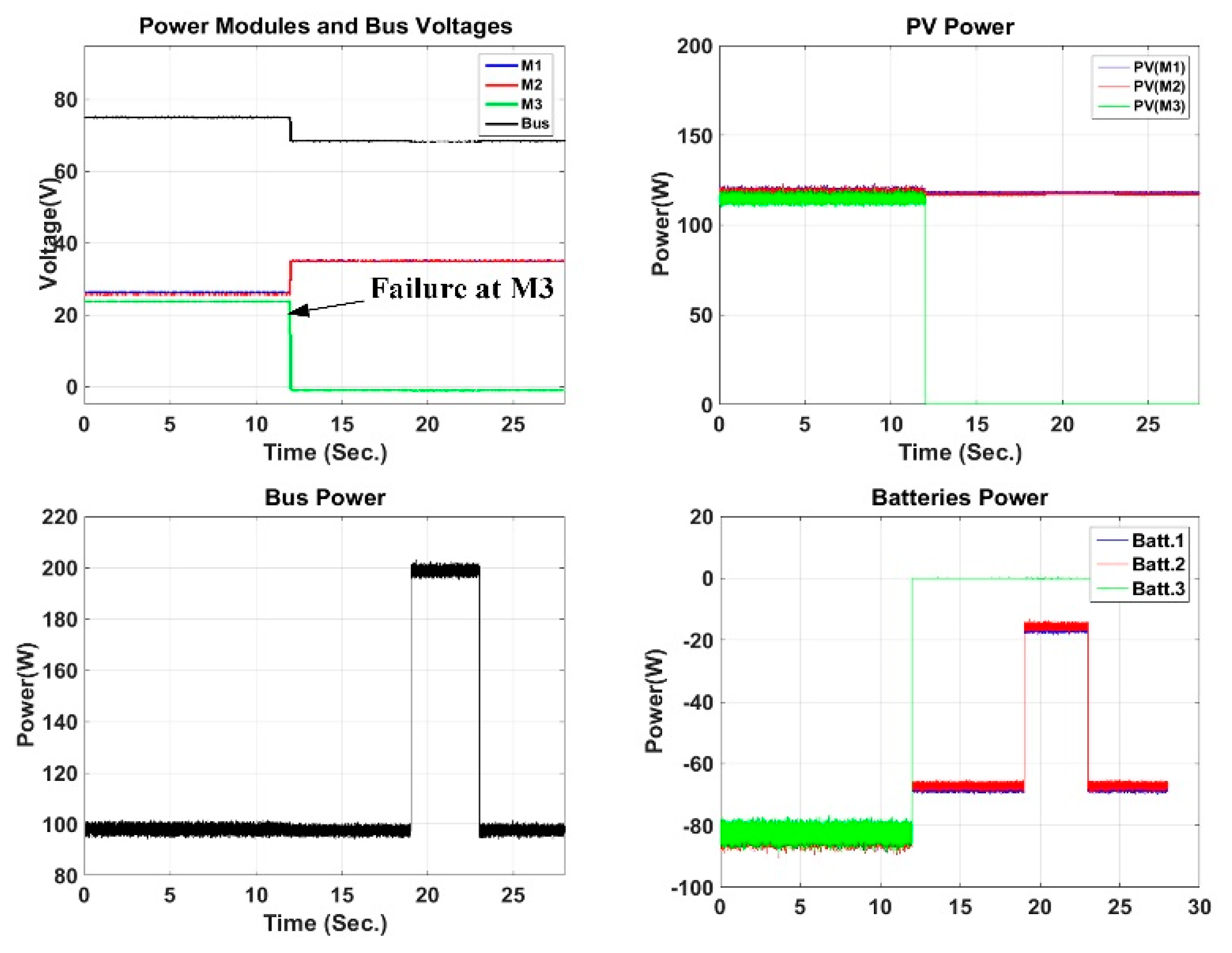
The last test is shown in Figure 14, where the operation of the MMPC for a single module failure was investigated. At t = 12 s, a failure had been imposed to the MMPC by disconnecting the PV-source and the battery of M3. As can be seen, the collapse of M3 voltage caused the MMPC to immediately respond by increasing the voltage contribution of M1 and M2 to the maximum level to compensate for the loss of the M3 and to attempt to maintain the bus voltage at the nominal value. However, as the maximum voltage contribution of the power modules is limited to the battery voltage (36 V), the maximum reachable bus voltage was less than 72 V, which is less than the specified value (75 V). This means that if the system had consisted of a sufficient number of modules, or if the battery module rated voltage were slightly higher, it would have been possible to completely compensate for the loss of one module while maintaining the bus voltage at its specified value. Increased loading also had been applied (19 s < t < 23 s) to verify the effect of this failure at different loads.
6. Conclusions
A new modular multiport converter for photovoltaic-battery based power systems has been proposed in this paper. The proposed converter topology is based on a modular architecture. Compared to conventional centralized multiport converter, this solution is able to operate with a high degree of PV power imbalance while reducing/maintaining the battery SoC imbalance/balancing. It can also accommodate partial failure of a module. The converter topology operation and control are derived. The proposed converter has been prototyped at 75 V/1 kW based on three modules to validate the concept. The experimental results showed the performance of the proposed converter confirming the expected benefits including capability to achieve battery balancing while operating with PV power imbalance or with a module fault.
As a stepping stone, this study opens a new approach for using modular architectures of multiport power converters to enable the use of low voltage/high current photovoltaic modules and battery modules to implement a high voltage power system bus instead of using high voltage strings made of a large number of series-connected PV-modules and battery cells with the related known problems. Additionally, due to the low voltage stress on the semiconductor devices in the proposed converter, low voltage rating semiconductor switches with reduced parasitic capacitances and ON-resistances can be used within the converter modules which may reduce switching/conduction power losses, improving overall efficiency compared to using higher voltage rated power devices.
Author Contributions
Conceptualization, all; investigation and validation, A.M.F.; writing—original draft preparation, A.M.F.; writing—review and editing, C.K. and M.S.; supervision, C.K. and M.S.
Funding
This research was funded by Ministry of Higher Education, Egypt through PhD scholarship funded by Cultural Affairs and Missions Sector.
Conflicts of Interest
The authors declare no conflicts of interest.
References
- Saxena, N.; Singh, B.; Vyas, A.L. Single-phase SOLAR PV SYSTEM with battery and exchange of power in grid-connected and standalone modes. IET Renew. Power Gener. 2017, 11, 325–333. [Google Scholar] [CrossRef]
- Maheswari, L.; Rao, P.S.; Sivakumaran, N.; Ilango, G.S.; Nagamani, C. A control strategy to enhance the life time of the battery in a stand-alone PV system with DC loads. IET Power Electron. 2017, 10, 1087–1094. [Google Scholar] [CrossRef]
- Chao, K.H.; Huang, C.H. Bidirectional DC-DC soft-switching converter for stand-alone photovoltaic power generation systems. IET Power Electron. 2014, 7, 1557–1565. [Google Scholar] [CrossRef]
- Locment, F.; Sechilariu, M.; Houssamo, I. DC Load and Batteries Control Limitations for Photovoltaic Systems Experimental Validation. IEEE Trans. Power Electron. 2012, 27, 4030–4038. [Google Scholar] [CrossRef]
- Liu, D.; Li, H. A ZVS Bi-Directional DC-DC Converter for Multiple Energy Storage Elements. IEEE Trans. Power Electron. 2006, 21, 1513–1517. [Google Scholar] [CrossRef]
- Yaow-Ming, C.; Yuan-Chuan, L.; Feng-Yu, W. Multi-input DC/DC converter based on the multiwinding transformer for renewable energy applications. IEEE Trans. Ind. Appl. 2002, 38, 1096–1104. [Google Scholar] [CrossRef]
- Zhao, C.; Round, S.D.; Kolar, J.W. An Isolated Three-Port Bidirectional DC-DC Converter with Decoupled Power Flow Management. IEEE Trans. Power Electron. 2008, 23, 2443–2453. [Google Scholar] [CrossRef]
- Krishnaswami, H.; Mohan, N. Three-Port Series-Resonant DC-DC Converter to Interface Renewable Energy Sources with Bidirectional Load and Energy Storage Ports. IEEE Trans. Power Electron. 2009, 24, 2289–2297. [Google Scholar] [CrossRef]
- Wu, H.; Chen, R.; Zhang, J.; Xing, Y.; Hu, H.; Ge, H. A Family of Three-Port Half-Bridge Converters for a Stand Alone Renewable Power System. IEEE Trans. Power Electron. 2011, 26, 2697–2706. [Google Scholar] [CrossRef]
- Qian, Z.; Abdel-Rahman, O.; Batarseh, I. An Integrated Four-Port DC/DC Converter for Renewable Energy Applications. IEEE Trans. Power Electron. 2010, 25, 1877–1887. [Google Scholar] [CrossRef]
- Qian, Z.; Abdel-Rahman, O.; Al-Atrash, H.; Batarseh, I. Modeling and Control of Three-Port DC/DC Converter Interface for Satellite Applications. IEEE Trans. Power Electron. 2010, 25, 637–649. [Google Scholar] [CrossRef]
- Al-Atrash, H.; Tian, F.; Batarseh, I. Tri-Modal Half-Bridge Converter Topology for Three-Port Interface. IEEE Trans. Power Electron. 2007, 22, 341–345. [Google Scholar] [CrossRef]
- Li, Y.; Zhao, C.; Chen, J.Y.; Du, R.; Zhang, Y. Optimizing design of soft-switching dual-input full-bridge DC/DC converter. In Proceedings of the 2011 IEEE Vehicle Power and Propulsion Conference, Chicago, IL, USA, 6–9 September 2011. [Google Scholar]
- Yang, D.; Ruan, X.; Li, Y.; Liu, F. Multiple-input full bridge dc/dc converter. In Proceedings of the 2009 IEEE Energy Conversion Congress and Exposition, San Jose, CA, USA, 20–24 September 2009. [Google Scholar]
- Wu, H.; Sun, K.; Ding, S.; Xing, Y. Topology derivation of nonisolated three-port DC-DC converters from DIC and DOC. IEEE Trans. Power Electron. 2013, 28, 3297–3307. [Google Scholar] [CrossRef]
- Wu, H.; Xing, Y.; Xia, Y.; Sun, K. A family of non-isolated three-port converters for stand-alone renewable power system. In Proceedings of the IECON 2011—37th Annual Conference of the IEEE Industrial Electronics Society, Melbourne, Australia, 7–10 November 2011. [Google Scholar]
- Zhu, H.; Zhang, D.; Zhang, B.; Zhou, Z. A Nonisolated Three-Port DC-DC Converter and Three-Domain Control Method for PV-Battery Power Systems. IEEE Trans. Ind. Electron. 2015, 62, 4937–4947. [Google Scholar] [CrossRef]
- Wu, H.; Zhang, J.; Xing, Y. A Family of Multiport Buck-Boost Converters Based on DC-Link-Inductors (DLIs). IEEE Trans. Power Electron. 2015, 30, 735–746. [Google Scholar] [CrossRef]
- Nejabatkhah, F.; Danyali, S.; Hosseini, S.H.; Sabahi, M.; Niapour, S.M. Modeling and Control of a New Three-Input DC-DC Boost Converter for Hybrid PV/FC/Battery Power System. IEEE Trans. Power Electron. 2012, 27, 2309–2324. [Google Scholar] [CrossRef]
- Chen, Y.; Wen, G.; Peng, L.; Kang, Y.; Chen, J. A family of cost-efficient non-isaolated single-inductor three-port converters for low power stand-alone renewable power applications. In Proceedings of the 2013 Twenty-Eighth Annual IEEE Applied Power Electronics Conference and Exposition (APEC), Long Beach, CA, USA, 17–21 March 2013. [Google Scholar]
- Anuradha, C.; Vel, C.; Venkatesan, T. Analysis of Non-Isolated Multi-Port Single Ended Primary Inductor Converter for Standalone Applications. Energies 2018, 11, 539. [Google Scholar] [CrossRef]
- Anuradha, C.; Chellammal, N.; Saquib Maqsood, M.; Vijayalakshmi, S. Design and Analysis of Non-Isolated Three-Port SEPIC Converter for Integrating Renewable Energy Sources. Energies 2019, 12, 221. [Google Scholar] [CrossRef]
- Zhang, N.; Sutanto, D.; Muttaqi, K.M. A review of topologies of three-port DC–DC converters for the integration of renewable energy and energy storage system. Renew. Sustain. Energy Rev. 2016, 56, 388–401. [Google Scholar] [CrossRef]
- Mäki, A.; Valkealahti, S. Power Losses in Long String and Parallel-Connected Short Strings of Series-Connected Silicon-Based Photovoltaic Modules Due to Partial Shading Conditions. IEEE Trans. Energy Convers. 2012, 27, 173–183. [Google Scholar] [CrossRef]
- Sullivan, C.R.; Awerbuch, J.; Latham, A.M. Decrease in photovoltaic power output from ripple: Simple general calculation and effect of partial shading. In Proceedings of the 2011 Twenty-Sixth Annual IEEE Applied Power Electronics Conference and Exposition (APEC), Fort Worth, TX, USA, 6–11 March 2011. [Google Scholar]
- Li, Y.; Oruganti, R. A Low Cost Flyback CCM Inverter for AC Module Application. IEEE Trans. Power Electron. 2012, 27, 1295–1303. [Google Scholar] [CrossRef]
- Kadri, R.; Gaubert, J.P.; Champenois, G. Nondissipative String Current Diverter for Solving the Cascaded DC-DC Converter Connection Problem in Photovoltaic Power Generation System. IEEE Trans. Power Electron. 2012, 27, 1249–1258. [Google Scholar] [CrossRef]
- Gogoana, R.; Pinson, M.B.; Bazant, M.Z.; Sarma, S.E. Internal resistance matching for parallel-connected lithium-ion cells and impacts on battery pack cycle life. J. Power Sources 2014, 252, 8–13. [Google Scholar] [CrossRef]
- Wen, S. Cell balancing buys extra run time and battery life. Analog Appl. J. 2009, 14–18. Available online: http://focus.ti.com/lit/an/slyt322/slyt322.pdf (accessed on 1 September 2019).
- Fares, A.; Klumpner, C.; Sumner, M. Investigating the benefits and limitations of cascaded converter topologies used in modular battery systems. In Proceedings of the 2017 IEEE 26th International Symposium on Industrial Electronics (ISIE), Edinburgh, UK, 19–21 June 2017. [Google Scholar]
- Lu, L.; Han, X.; Li, J.; Hua, J.; Ouyang, M. A review on the key issues for lithium-ion battery management in electric vehicles. J. Power Sources 2013, 226, 272–288. [Google Scholar] [CrossRef]
- Fares, A.M.; Klumpner, C.; Sumner, M. Development of a battery energy loss observer based on improved equivalent circuit modelling. In Proceedings of the 2016 18th European Conference on Power Electronics and Applications (EPE’16 ECCE Europe), Karlsruhe, Germany, 5–9 September 2016. [Google Scholar]
- Qian, Z.; Abdel-Rahman, O.; Pepper, M.; Batarseh, I. Analysis and design for paralleled three-port DC/DC converters with democratic current sharing control. In Proceedings of the 2009 IEEE Energy Conversion Congress and Exposition, San Jose, CA, USA, 20–24 September 2009. [Google Scholar]
- Song, S.; Li, W.; Ni, K.; Xu, H.; Hu, Y.; Si, J. Modular Multi-Port Ultra-High Power Level Power Converter Integrated with Energy Storage for High Voltage Direct Current (HVDC) Transmission. Energies 2018, 11, 2711. [Google Scholar] [CrossRef]
- Strickland, D.; Chittock, L.; Stone, D.A.; Foster, M.P.; Price, B. Estimation of Transportation Battery Second Life for Use in Electricity Grid Systems. IEEE Trans. Sustain. Energy 2014, 5, 795–803. [Google Scholar] [CrossRef] [Green Version]
- Gladwin, D.T.; Gould, C.R.; Stone, D.A.; Foster, M.P. Viability of second-life use of electric and hybridelectric vehicle battery packs. In Proceedings of the IECON 2013—39th Annual Conference of the IEEE Industrial Electronics Society, Vienna, Austria, 10–13 November 2013. [Google Scholar]
- Mukherjee, N.; Strickland, D. Analysis and Comparative Study of Different Converter Modes in Modular Second-Life Hybrid Battery Energy Storage Systems. IEEE J. Emerg. Sel. Top. Power Electron. 2016, 4, 547–563. [Google Scholar] [CrossRef]
- Fares, A.M.; Klumpner, C.; Sumner, M. Optimising the structure of a cascaded modular battery system for enhancing the performance of battery packs. J. Eng. 2019, 2019, 3862–3866. [Google Scholar] [CrossRef]
Figure 1.
Power system structure with (a) multiple single DC-DC converters; (b) Conventional centralized multiport DC-DC converter; (c) proposed modular multiport DC-DC converter.
Figure 1.
Power system structure with (a) multiple single DC-DC converters; (b) Conventional centralized multiport DC-DC converter; (c) proposed modular multiport DC-DC converter.

Figure 2.
The proposed modular multiport converter architecture.

Figure 3.
Suggested topologies of the multi-port converter (a) Boost-Boost MPC; (b) proposed topology.
Figure 3.
Suggested topologies of the multi-port converter (a) Boost-Boost MPC; (b) proposed topology.

Figure 4.
Current flow paths for operating stages in single input double output mode: (a) Stage I; (b) Stage II; and (c) Stage III.
Figure 4.
Current flow paths for operating stages in single input double output mode: (a) Stage I; (b) Stage II; and (c) Stage III.

Figure 5.
Typical waveforms for single input double output mode for continuous conduction mode.

Figure 6.
Current flow paths of operating stages in DISO mod: (a) Stage I; (b) Stage II; (c) Stage III.
Figure 6.
Current flow paths of operating stages in DISO mod: (a) Stage I; (b) Stage II; (c) Stage III.

Figure 7.
Typical waveforms in DISO mode at CCM.

Figure 8.
Block diagram of the proposed MMPC.

Figure 9.
Block diagram of MMPC local control loop.

Figure 10.
Experimental setup for testing of the proposed modular multiport converter.

Figure 11.
Managing battery charge balancing under unbalanced power from PVs.

Figure 12.
Bus voltage control under availability/unavailability of PV power.

Figure 13.
Reducing state of charge imbalance of the battery modules under various conditions (PVs power imbalances, load power surges, no sunlight).
Figure 13.
Reducing state of charge imbalance of the battery modules under various conditions (PVs power imbalances, load power surges, no sunlight).

Figure 14.
Operation of the proposed modular multiport converter with one module failure.


Table 1.
Design parameters of the experimental setup.
| Symbol | Description | Value |
|---|---|---|
| Vbatt | Battery module voltage | 36 V |
| VPV-max | PV-module voltage at MPP | 17 V |
| L1 | Battery converter inductor | 375 μH |
| L2 | PV-converter inductor | 187 μH |
| M | Total number PM | 3 |
| Ibus | Maximum load current | 14 A |
| Vbus | Bus voltage | 75 V |
| fs | Switching frequency | 10 kHz |
© 2019 by the authors. Licensee MDPI, Basel, Switzerland. This article is an open access article distributed under the terms and conditions of the Creative Commons Attribution (CC BY) license (http://creativecommons.org/licenses/by/4.0/).
Share and Cite
MDPI and ACS Style
Fares, A.M.; Klumpner, C.; Sumner, M. A Novel Modular Multiport Converter for Enhancing the Performance of Photovoltaic-Battery Based Power Systems. Appl. Sci. 2019, 9, 3948. https://doi.org/10.3390/app9193948
AMA Style
Fares AM, Klumpner C, Sumner M. A Novel Modular Multiport Converter for Enhancing the Performance of Photovoltaic-Battery Based Power Systems. Applied Sciences. 2019; 9(19):3948. https://doi.org/10.3390/app9193948
Chicago/Turabian StyleFares, Ahmed M, Christian Klumpner, and Mark Sumner. 2019. "A Novel Modular Multiport Converter for Enhancing the Performance of Photovoltaic-Battery Based Power Systems" Applied Sciences 9, no. 19: 3948. https://doi.org/10.3390/app9193948
Note that from the first issue of 2016, this journal uses article numbers instead of page numbers. See further details here.