Near-Field IR Orientational Spectroscopy of Silk
by
 and
and
Meguya Ryu
1, 
Reo Honda
1,
Aina Reich
2,
Adrian Cernescu
2,
Jing-Liang Li
3, 
Jingwen Hu
4,5,
Saulius Juodkazis
4,5,6,* and
Junko Morikawa
1,6,* 1
School of Materials and Chemical Technology, Tokyo Institute of Technology, 2-12-1, Ookayama, Meguro-ku, Tokyo 152-8550, Japan
2
Neaspec GmbH, Bunsenstrasse 5, 82152 Martinsried, Germany
3
Institute for Frontier Materials, Deakin University, Geelong, VIC 3220, Australia
4
Swinburne University of Technology, John st., Hawthorn, VIC 3122, Australia
5
Melbourne Center for Nanofabrication, Australian National Fabrication Facility, Clayton, VIC 3168, Australia
6
Tokyo Tech World Research Hub Initiative (WRHI), School of Materials and Chemical Technology, Tokyo Institute of Technology, 2-12-1, Ookayama, Meguro-ku, Tokyo 152-8550, Japan
*
Authors to whom correspondence should be addressed.
Appl. Sci. 2019, 9(19), 3991; https://doi.org/10.3390/app9193991
Submission received: 30 August 2019
/
Revised: 17 September 2019
/
Accepted: 20 September 2019
/
Published: 24 September 2019
(This article belongs to the Section Nanotechnology and Applied Nanosciences)
Abstract
:Orientational dependence of the IR absorbing amide bands of silk is demonstrated from two orthogonal longitudinal and transverse microtome slices with a thickness of only ∼100 nm. Scanning near-field optical microscopy (SNOM) which preferentially probes orientation perpendicular to the sample’s surface was used. Spatial resolution of the silk–epoxy boundary was ∼100 nm resolution, while the spectra were collected by a ∼10 nm tip. Ratio of the absorbance of the amide-II C-N at 1512 cm and amide-I C=O -sheets at 1628 cm showed sensitivity of SNOM to the molecular orientation. SNOM characterisation is complimentary to the far-field absorbance which is sensitive to the in-plane polarisation. Volumes with cross sections smaller than 100 nm can be characterised for molecular orientation. A method of absorbance measurements at four angles of the slice cut orientation, which is equivalent to the four polarisation angles absorbance measurement, is proposed.

1. Introduction
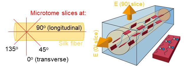
Nanofabrication with a resolution of few nanometers has now become common using electron emission [1] and thermal probes [2,3]. Structuring of materials with nanoscale precision requires equally matching or better characterisation capabilities. Structural anisotropy of materials underpin their optical, thermal and mechanical properties, and have to be determined at the highest transverse and longitudinal resolutions [4,5]. For example, a fibril of silk tens-of-nanometers in diameter defines its thermal properties [6]. Comparable IR absorbance spectra of silk were obtained using three different methods [7]: (i) a table-top Fourier transform infrared (FTIR) in transmission, (ii) a synchrotron-based attenuated total reflection (ATR) FTIR, and (iii) an atomic force microscopy (AFM) with a tip that responds to the IR absorbed light, also known as nano-IR [8]. The AFM-based nano-IR technique acquires structural information at the nanoscale, the area under the AFM tip forms a volume with a lateral cross-section of ∼20 nm. Different sensitivity of reflectance R and absorbance A to the real and imaginary parts of refractive index becomes important. The far-field absorbance is defined by , while the near-field ATR-FTIR mode is affected by n due to the Snell’s law [9,10]. Another tip-based near-field optical charactrisation technique, scanning near-field optical microscopy (SNOM), is a popular method to map surface topography and refractive index decoupled from the scattered light. Typically, a p-polarised light with E-field aligned with the tip and perpendicular to the probed surface defines the strongest coupling and field enhancement. It is noteworthy, that the E-field component is absent in the paraxial geometry used for transmission measurements but present only under the most tight optical focusing conditions. SNOM allows probing of a material with E-field normal to the surface and was used in this study to test orientational sensitivity of this method to the alignment of amide bands in silk sliced along and across the fiber, the longitudinal and transverse cuts at and orientation angles, correspondingly.
Here, we used scattering SNOM to probe and to determine spectral differences due to orientation in the absorbance at the amide bands of silk fibers. Cross-sections of silk fibers at and cut-orientations were prepared using ultramicrotome. Silk was chosen due to its well known spectral properties and uniaxial symmetry which can be examined from longitudinal and transverse microtome slices [6]. Sub-wavelength resolutions in hyperspectral IR mapping of absorbance and orientational properties of the absorption bands were measured from 100-nm-thick slices of silk.
2. Methods and Samples
2.1. Silk Slices
Preparation of white silk Bombyx mori fibers was the same as described previously [11]. In short, the cocoons were boiled three times in an aqueous 0.5% (w/v) NaCO solution to remove the sericin. The degummed silk fibers were rinsed with warm ultra pure water at 60 C thoroughly to remove the residual sercin and dried at room temperature.
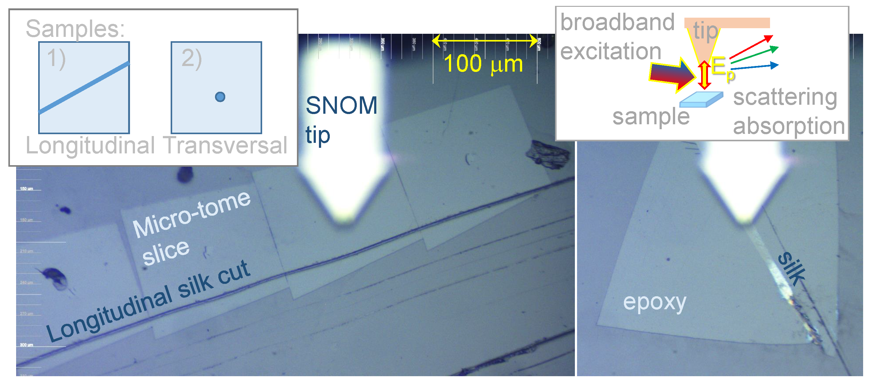
Silk fibers were embedded in epoxy resin (Oken Ltd., Tokyo, Japan) and thin-sectioned by ultramicrotomy to achieve a sample thickness of ∼100 nm. Slices at (transverse) and (longitudinal) cut-orientations were then immobilised on a gold mirror for measurements (Figure 1).
2.2. IR Spectral Measurements
The sub-diffraction scattering (s-)SNOM (neaspec GmbH) uses a metalised AFM tip which simultaneously maps the surface relief (topography) by its basic AFM operation and under external IR illumination (broadband laser working by difference-frequency generation, Toptica), acts as a light-concentrating antenna such that the sample is probed with a nanofocused light field. The AFM tapping mode operation (ca. 60 nm amplitude) modulates the near-field interaction between the tip and sample [12]. The measured nano-IR absorbance is proportional to the imaginary part of the scattering coefficient , which relates the light scattered field , and the incident field through the equation , where and are the amplitude and phase of the back-scattered spectra [10]. Using the asymmetric Michelson interferometer, the full complex function of the scattered optical signal can be recorded, therefore enabling the simultaneous measurement of both nano-IR absorbance and reflectivity spectra [10]. The Michelson interferometer and a lock-in detection of the signal at higher harmonic of the tapping frequency ∼250 kHz provides background-free nano-IR spectra and images with maximum resolution imposed by the AFM tip size independent of the laser wavelength [10].
The nano-FTIR spectra were recorded in ∼100 s/spectrum with a spectral resolution of 10 cm. Removal of the instrumental response function from the nano-FTIR spectra was done by normalization of the measured spectra to a reference Si signal. Resulting nano-FTIR absorbance and reflectivity spectra are directly correlated with the standard far-field IR spectra [13,14].
3. Results and Discussion
Dimensions of crystalline -sheet fibrils in silk fibers is ≃10 nm [15]. SNOM measurements are well suited to measure n and from areas of comparable dimensions [11]. Whether it was possible to determine optical anisotropy due to molecular orientation using a point-like excitation source was the motivation of this study. If the anisotropy of absorbance (dichroism ) and refractive index (birefringence ) could be measured with a point-like source using s-SNOM, this would open the possibility of determining anisotropy and molecular orientation with sub-wavelength resolution at nanoscale.
The birefringence originates from the alignment of molecular bonds or secondary ordering and can be detected at different spectral ranges [16]. Molecular alignment of the amide-II at 1512 cm (C-N) and amide-I -sheets at 1628 cm (C=O) was measured from micron-thick longitudinal silk slices [17]. In-plane perpendicular orientation between C=O and C-N bonds was revealed [17] using a longitudinal slice of silk fiber, which facilitated fidelity of measurements due to uniformity of thickness [18].
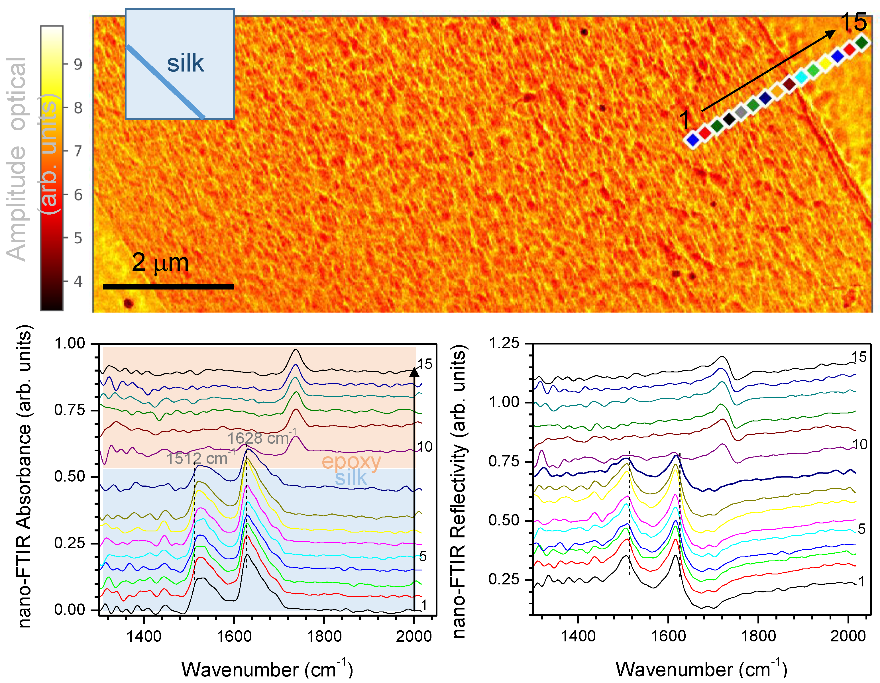
In this study s-SNOM data was collected in the IR spectral range together with topography map (Figure 2). The mechanical amplitude and phase are related to the stability of the feedback loop and were used as a qualitative error signal, i.e., unexpected changes in the mechanical amplitude correlated with errors in the near-field amplitude. The optical amplitude map is also shown (Figure 2) and is dominated by the reflectivity of the surface, which is usually very low for the polymers (emissivity is high at the absorption bands). Both, mechanical and optical mapping revealed a clear boundary between the longitudinal (-cut) silk fiber slice and surrounding epoxy (Figure 2). Recently, it was demonstrated that mechanical viscoelastic parameters: the Young’s modulus, viscosity coefficient, and retardation time can be determined using the amplitude modulated–frequency modulated (AM-FM) mode of cantilever response [19] and are linked to the topography of the sample via the offset of the tapping mode signal.
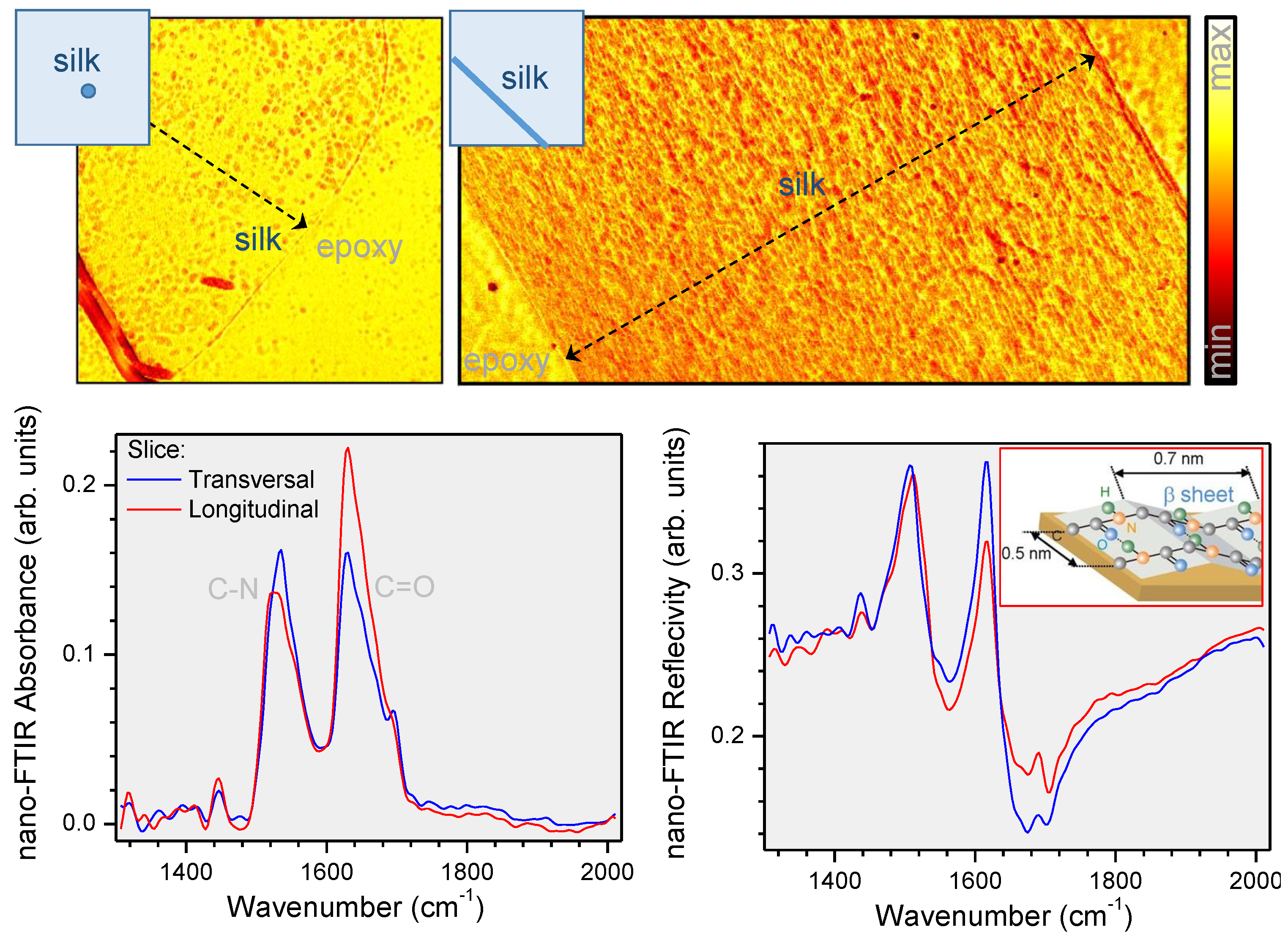
The amide I and II bands [11] were well recognisable in the nano-FTIR absorbance spectra collected from different single measurements points (Figure 2). Measurements were made along 3 m linear scan with a separation of 200 nm between the measurement sites. Clear transition from the silk to epoxy was observed and a half-step can be defined as the upper bound of the resolution (Figure 3).
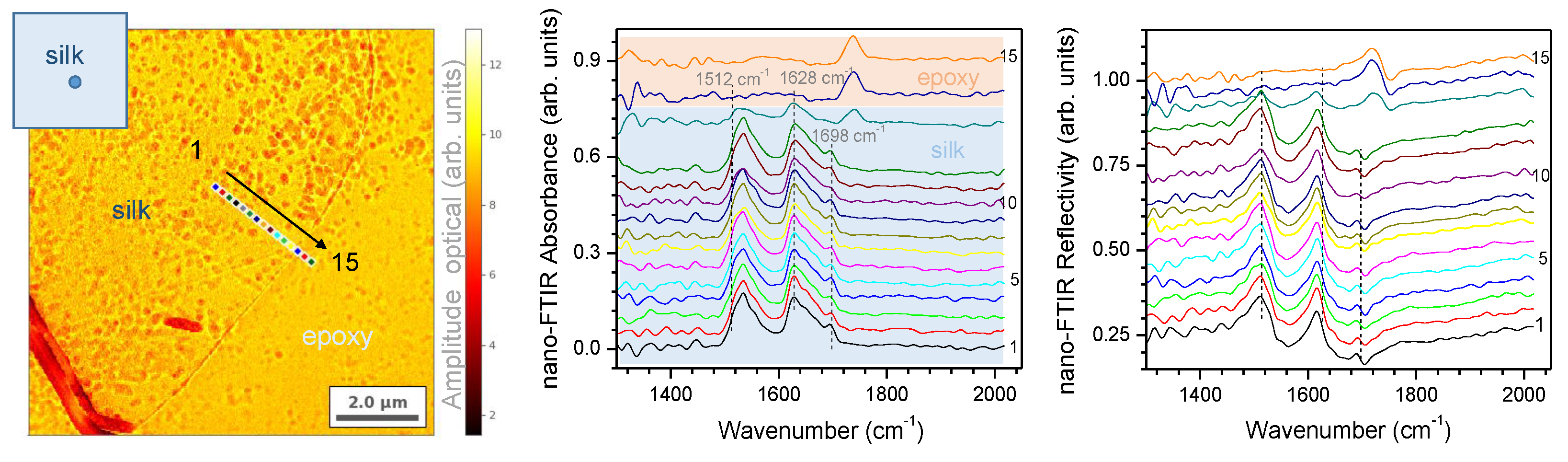
The transverse silk slice (-cut) showed similar topography and mechanical (amplitude and phase) mapping with a slightly larger reflectivity (Figure 4). The same scan along the line showed a distinct transition from silk to epoxy. The dark regions along the boundary were observed with spectral features mixed between silk and epoxy (Figure 4). Since the 100 nm thickness of the slice was only approximately twice larger than the diameter of the fiber, mechanical cracks were expected under sheer forces applied during slicing.
Comparison of spectra measured from transverse () and longitudinal () slices is shown in Figure 5. Different the amide-II and I bands ratios are directly related to the orientation as we showed by the far-field absorbance [17]. For the longitudinal slice, C=O (amide-I) is radially distributed and most strongly coupled to the of the SNOM needle, while C-N (amide-II) is perpendicular to the SNOM tip, hence, uncoupled to the absorbing dipole. The inset in the reflectivity spectum (Figure 5) shows mutually perpendicular in-plane orientations of the C=O and C-N amide bands on the longitudinal slice; note, the C=O is radially distributed if observed out-of-plane. This illustration also clarifies that for the transverse slice (C-N) and perpendicular (C=O). The two transverse and longitudinal slices represents two cases when is most strongly coupled to one or the other amide bands. The different ratio of the heights of the two amide absorbance peaks (Figure 5) is directly related to the different orientation as we observed in the far-field measurements [17]. Also, observation of a side-lobe peak at 1698 cm is related to the -sheet amide [17] and was only observed in the transverse slice (Figure 4).
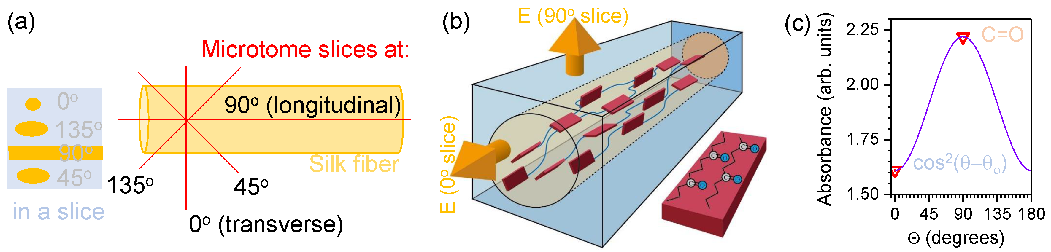
This first qualitative result shows that it is possible to detect orientational differences in molecular alignment from single point measurements using tip source of excitation. Further efforts should be concentrated to develop near-field four-polarisation analogy of orientation mapping (Figure 6) which for absorbance has been developed for the far field [20]. As demonstrated recently, the orientational dependence of transmittance/absorbance can be used to separate contributions due to the real and imaginary parts of refractive index [21]. Birefringence and dichroism, both being orientation dependent can be separated by the four-angle absorbance method [21]. Here we show a concept analogous to this four-angle method whereby the orientation of the absorbers in the sample, for an E-field perpendicular to the sample’s surface (SNOM geometry), is determined using microtome cuts of different orientations and is illustrated in Figure 6c. Structural knowledge of molecular alignment is usually obtained by X-ray diffraction (XRD), but can now be obtained by direct near-field measurements with spatial resolution down to tens-of-nm (Figure 6b).
4. Conclusions and Outlook
In summary, spectral characterisation, lateral mapping of nano-IR absorbance and reflectance with deep sub-wavelength resolution in the IR molecular finger printing window was demonstrated using thin (100 nm) transverse and longitudinal slices of silk. Hyper-spectral mapping across the silk fiber slice was obtained with high accuracy and reproducibility. The possibility of orientation measurements using a SNOM tip is proposed and demonstrated at two angles (two slices of silk fiber) using the amide bands and previously measured far-field IR spectra. Since preparation of thin microtome slices of soft bio-materials does not alter their structure [11], this opens the possibility of measuring optical properties from nano-volumes prepared by careful alignment of microtome cuts. One can envisage that using slices of silk fiber at different angles (transverse), , and (longitudinal), the four-orientation mapping equivalent to the four-polarisation method [20] can be developed and will be focus of a future study. Measurement of orientation changes in the regions of laser-induced material modification by re-melting [22], phase change and ablation [23] will benefit from the introduced method. Recently, orientation and ordering of phospholipids was demonstrated [24].
Author Contributions
Conceptualization, J.M., M.R., S.J.; methodology, M.R., J.M., A.C.; experiments and sample preparation, M.R., R.H., A.R., J.H., J.-L.L.; data analysis, all the authors; writing—review and editing, all the authors.
Funding
This research was funded by JSPS KAKENHI Grants No. 16K06768, 18H04506 (Japan) and the Australian Research Council Discovery projects DP1901032.
Acknowledgments
We are grateful for R. Kikuchi from Materials Analysis Division of Tokyo Institute of Technology, Ookayama, for his assistance with ultramicrotomy. S.J. is grateful for sabbatical stays at Tokyo Institute of Technology and Shizuoka University in 2018. We thank Soon Hock Ng and Vijay Kumar for the critical reading of the manuscript.
Conflicts of Interest
The authors declare no conflict of interest.
References
- Rangelow, I.W.; Ahmad, A.; Ivanov, T.; Kaestner, M.; Krivoshapkina, Y.; Angelov, T.; Lenk, S.; Lenk, C.; Ishchuk, V.; Hofmann, M.; et al. Pattern-generation and pattern-transfer for single-digit nano devices. J. Vac. Sci. Technol. B 2016, 34, 06K202. [Google Scholar] [CrossRef]
- Paul, P.C.; Knoll, A.W.; Holzner, F.; Despont, M.; Duerig, U. Rapid turnaround scanning probe nanolithography. Nanotechnology 2011, 22, 275306. [Google Scholar] [CrossRef]
- Holzner, F.; Paul, P.; Drechsler, U.; Despont, M.; Knoll, A.W.; Duerig, U. High density multi-level recording for archival data preservation. Appl. Phys. Lett. 2011, 99, 023110. [Google Scholar] [CrossRef]
- Shao, Z.; Vollrath, F. Surprising strength of silkworm silk. Nature 2002, 418, 741. [Google Scholar] [CrossRef]
- Jiang, J.; Zhang, S.; Qian, Z.; Qin, N.; Song, W.; Sun, L.; Zhou, Z.; Shi, Z.; Chen, L.; Li, X.; et al. Protein Bricks: 2D and 3D Bio-Nanostructures with Shape and Function on Demand. Adv. Mater. 2002, 30, 1705919. [Google Scholar] [CrossRef]
- Choi, S.H.; Kim, S.W.; Ku, Z.; Visbal-Onufrak, M.A.; Kim, S.R.; Choi, K.H.; Ko, H.; Choi, W.; Urbas, A.M.; Goo, T.W.; et al. Anderson light localization in biological nanostructures of native silk. Nat. Commun. 2018, 9, 452. [Google Scholar] [CrossRef] [Green Version]
- Ryu, M.; Kobayashi, H.; Balčytis, A.; Wang, X.; Vongsvivut, J.; Li, J.; Urayama, N.; Mizeikis, V.; Tobin, M.; Juodkazis, S.; et al. Nanoscale chemical mapping of laser-solubilized silk. Mater. Res. Express 2017, 4, 115028. [Google Scholar] [CrossRef] [Green Version]
- Dazzi, A.; Prazeres, R.; Glotin, F.; Ortega, J.M. Local infrared microspectroscopy with subwavelength spatial resolution with an atomic force microscope tip used as a photothermal sensor. Opt. Lett. 2005, 30, 2388–2390. [Google Scholar] [CrossRef]
- Bertie, E.; Michaelian, K.H. Comparison of infrared and Raman wave numbers of neat molecular liquids: Which is the correct infrared wavenumber to use? J. Chem. Phys. 1998, 109, 6764–6771. [Google Scholar] [CrossRef]
- Huth, F.; Schnell, M.; Wittborn, J.; Ocelic, N.; Hillenbrand, R. Infrared-spectroscopic nanoimaging with a thermal source. Nat. Mater. 2011, 10, 352–356. [Google Scholar] [CrossRef]
- Ryu, M.; Honda, R.; Cernescu, A.; Vailionis, A.; Balčytis, A.; Vongsvivut, J.; Li, J.; Linklater, D.; Ivanova, E.; Mizeikis, V.; et al. Nanoscale optical and structural characterisation of silk. Beilstein J. Nanotechnol. 2019, 10, 922–929. [Google Scholar] [CrossRef] [Green Version]
- Keilmann, F.; Hillenbrand, R. Near-field microscopy by elastic light scattering from a tip. Philos. Trans. R. Soc. Lond. A 2004, 362, 787–805. [Google Scholar] [CrossRef]
- Huth, F.; Govyadinov, A.; Amarie, S.; Nuansing, W.; Keilmann, F.; Hillenbrand, R. Nano-FTIR Absorption Spectroscopy of Molecular Fingerprints at 20 nm Spatial Resolution. Nano Lett. 2012, 12, 3973–3978. [Google Scholar] [CrossRef]
- Westermeier, C.; Cernescu, A.; Amarie, S.; Liewald, C.; Keilmann, F.; Nickel, B. Sub-micron phase coexistence in small-molecule organic thin films revealed by infrared nano-imaging. Nat. Commun. 2014, 5, 4101. [Google Scholar] [CrossRef] [Green Version]
- Drummy, L.F.; Farmer, B.L.; Naik, R.R. Correlation of the β-sheet crystal size in silk fibers with the protein amino acid sequence. Soft Matter 2007, 3, 877–882. [Google Scholar] [CrossRef]
- Balčytis, A.; Ryu, M.; Wang, X.; Novelli, F.; Seniutinas, G.; Du, S.; Wang, X.; Li, J.; Davis, J.; Appadoo, D.; et al. Silk: Optical Properties over 12.6 Octaves THz-IR-Visible-UV Range. Materials 2017, 10, 356. [Google Scholar] [CrossRef]
- Ryu, M.; Bačytis, A.; Wang, X.; Vongsvivut, J.; Hikima, Y.; Li, J.; Tobin, M.J.; Juodkazis, S.; Morikawa, J. Orientational Mapping Augmented Sub-Wavelength Hyper-Spectral Imaging of Silk. Sci. Rep. 2017, 7, 7419. [Google Scholar] [CrossRef]
- Honda, R.; Ryu, M.; Li, J.L.; Mizeikis, V.; Juodkazis, S.; Morikawa, J. Simple multi-wavelength imaging of birefringence: Case study of silk. Sci. Rep. 2002, 8, 17652. [Google Scholar] [CrossRef]
- Benaglia, S.; Amo, C.A.; Garcia, R. Fast, quantitative and high resolution mapping of viscoelastic properties with bimodal AFM. Nanoscale 2019, 11, 15289–15297. [Google Scholar] [CrossRef] [Green Version]
- Hikima, Y.; Morikawa, J.; Hashimoto, T. FT-IR Image Processing Algorithms for In-Plane Orientation Function and Azimuth Angle of Uniaxially Drawn Polyethylene Composite Film. Macromolecules 2011, 44, 3950–3957. [Google Scholar] [CrossRef]
- Ryu, M.; Honda, R.; Balcytis, A.; Vongsvivut, J.; Tobin, M.; Juodkazis, S.; Morikawa, J. Hyperspectral mapping of anisotropy. Nanoscale Horizons 2019. [Google Scholar] [CrossRef]
- Vanagas, E.; Kudryashov, I.; Tuzhilin, D.; Juodkazis, S.; Matsuo, S.; Misawa, H. Surface nanostructuring of borosilicate glass by femtosecond nJ energy pulses. Appl. Phys. Lett. 2003, 82, 2901–2903. [Google Scholar] [CrossRef]
- Yamasaki, K.; Juodkazis, S.; Matsuo, S.; Misawa, H. Three-dimensional microchannels in polymers: One step fabrication. Appl. Phys. A 2003, 77, 371–373. [Google Scholar] [CrossRef]
- Cernescu, A.; Szuwarzyński, M.; Kwolek, U.; Wydro, P.; Kepczynski, M.; Zapotoczny, S.; Nowakowska, M.; Quaroni, L. free infrared spectroscopy and imaging of single phospholipid bilayers with nanoscale resolution. Anal. Chem. 2018, 90, 1017910186. [Google Scholar] [CrossRef]
Figure 1.
Optical image of longitudinal micro-tome slices of Bombyx mori fibers. Left inset shows schematically the principle of spectrally broadband excitation and detection of scattered light implemented in neaspec tool for detection of nanoscale absorbance and scattering. The excitation light field is p-polarised, .

Figure 2.
Raw SNOM (neaspec) data from a longitudinal slice of Bombyx mori silk: topography (height: 0–92 nm), mechanical amplitude and phase, and optical amplitude (proportional to the reflectivity integrated over 1300–2020 cm) IR spectral range.
Figure 2.
Raw SNOM (neaspec) data from a longitudinal slice of Bombyx mori silk: topography (height: 0–92 nm), mechanical amplitude and phase, and optical amplitude (proportional to the reflectivity integrated over 1300–2020 cm) IR spectral range.

Figure 3.
Scattering SNOM mapping and point spectra at 15 locations separated on a line by 200 nm (color marked) measured on the longitudinal slice. The amplitude and phase of the measured spectra.
Figure 3.
Scattering SNOM mapping and point spectra at 15 locations separated on a line by 200 nm (color marked) measured on the longitudinal slice. The amplitude and phase of the measured spectra.

Figure 4.
Transverse slice of silk. SNOM map and the amplitude and phase of scattered field at 15 equidistant points across the silk–epoxy boundary.
Figure 4.
Transverse slice of silk. SNOM map and the amplitude and phase of scattered field at 15 equidistant points across the silk–epoxy boundary.

Figure 5.
SNOM maps of the transverse and longitudinal silk slices together with averaged nano-FTIR absorbance and reflectance spectra. Inset in reflectivity panel shows the molecular orientation of the amide-I,II bands in -sheet crystalline regions for the longitudinal slice (adopted form ref. [17]). Note, chemical bonding in the -sheets plane only is shown; the C=O bonds have a radial distribution along the fiber direction and their second order momentum distribution was determined in the Supplementary of ref. [17].

Figure 6.
(a) Concept of four-angle absorbance measurements where instead of polarisation, four different orientation micro-tome slices are prepared. In this study we carried out measurements on two and longitudinal and transverse slices, respectively. (b) Visualisation of the a silk fiber with its internal -sheet structure. (c) Orientation determination of C=O -sheet absorbers at 1628 cm using different orientation slices (data markets for the transverse and longitudinal data) microtome slices; is the initial orientation. Note, for quantitative determination of orientation, four orientation slices are required.

© 2019 by the authors. Licensee MDPI, Basel, Switzerland. This article is an open access article distributed under the terms and conditions of the Creative Commons Attribution (CC BY) license (http://creativecommons.org/licenses/by/4.0/).
Share and Cite
MDPI and ACS Style
Ryu, M.; Honda, R.; Reich, A.; Cernescu, A.; Li, J.-L.; Hu, J.; Juodkazis, S.; Morikawa, J. Near-Field IR Orientational Spectroscopy of Silk. Appl. Sci. 2019, 9, 3991. https://doi.org/10.3390/app9193991
AMA Style
Ryu M, Honda R, Reich A, Cernescu A, Li J-L, Hu J, Juodkazis S, Morikawa J. Near-Field IR Orientational Spectroscopy of Silk. Applied Sciences. 2019; 9(19):3991. https://doi.org/10.3390/app9193991
Chicago/Turabian StyleRyu, Meguya, Reo Honda, Aina Reich, Adrian Cernescu, Jing-Liang Li, Jingwen Hu, Saulius Juodkazis, and Junko Morikawa. 2019. "Near-Field IR Orientational Spectroscopy of Silk" Applied Sciences 9, no. 19: 3991. https://doi.org/10.3390/app9193991
Note that from the first issue of 2016, this journal uses article numbers instead of page numbers. See further details here.