The Performance of Zr-Doped Al-Zn-Sn-O Thin Film Transistor Prepared by Co-Sputtering

 , and
, and
Abstract
:1. Introduction
2. Materials and Methods
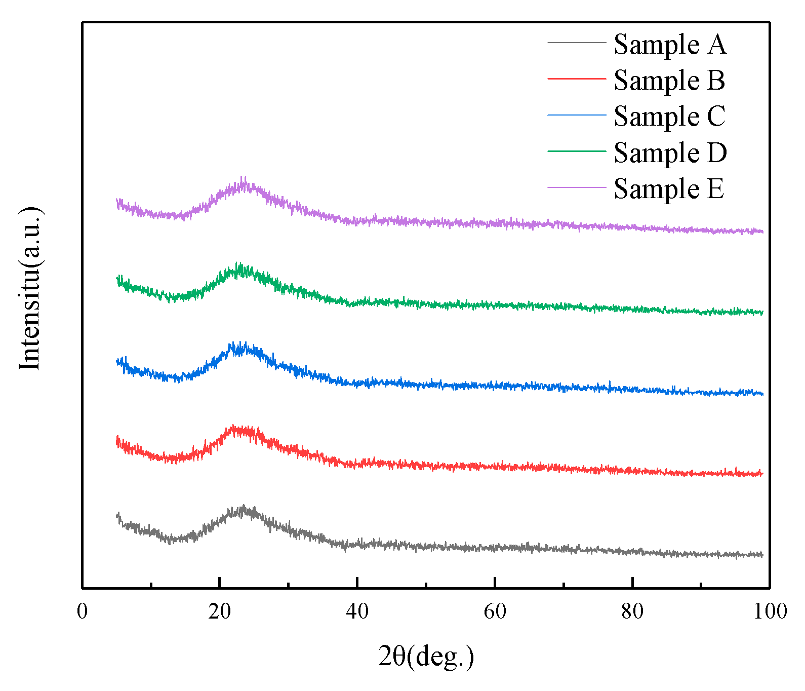
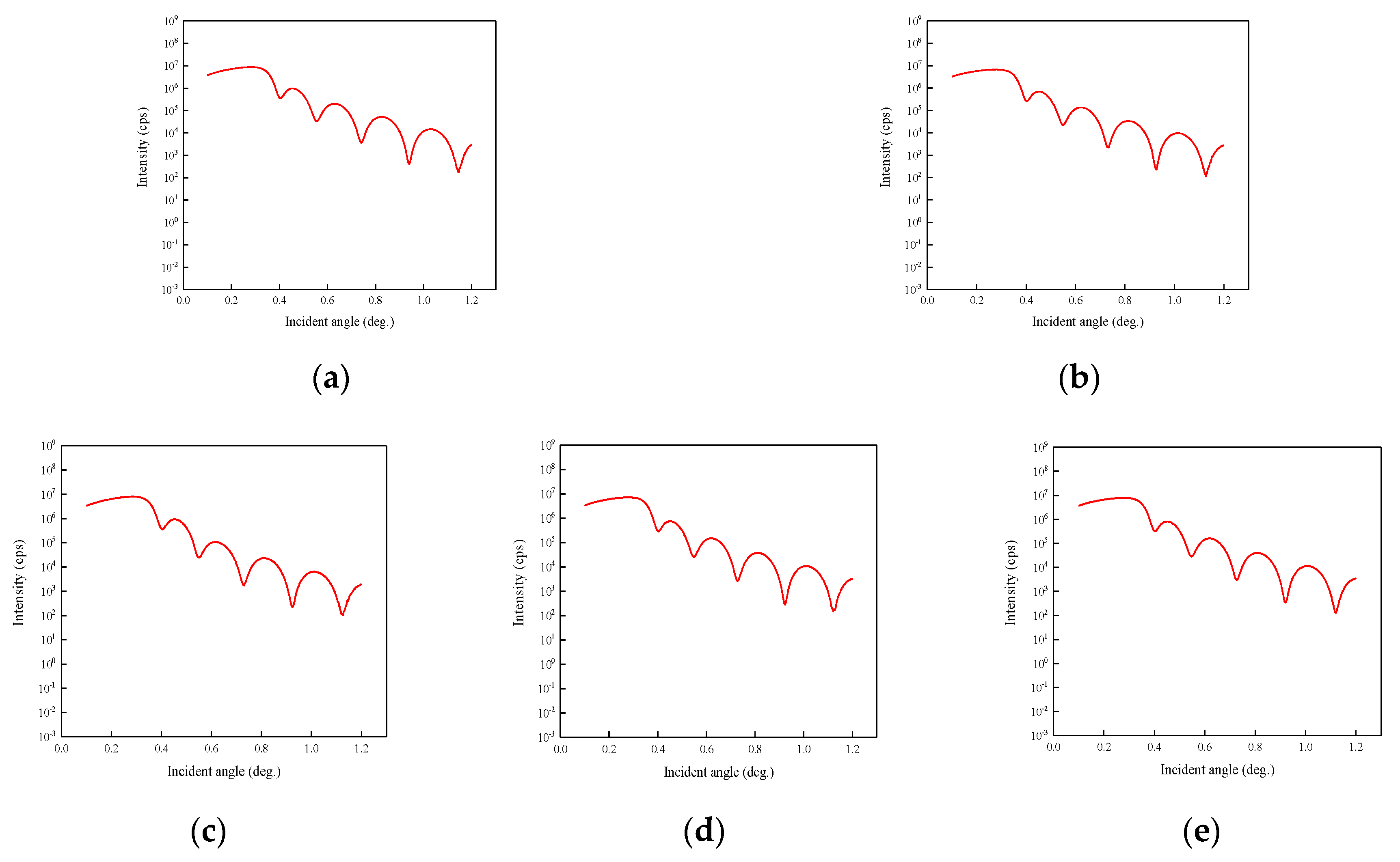
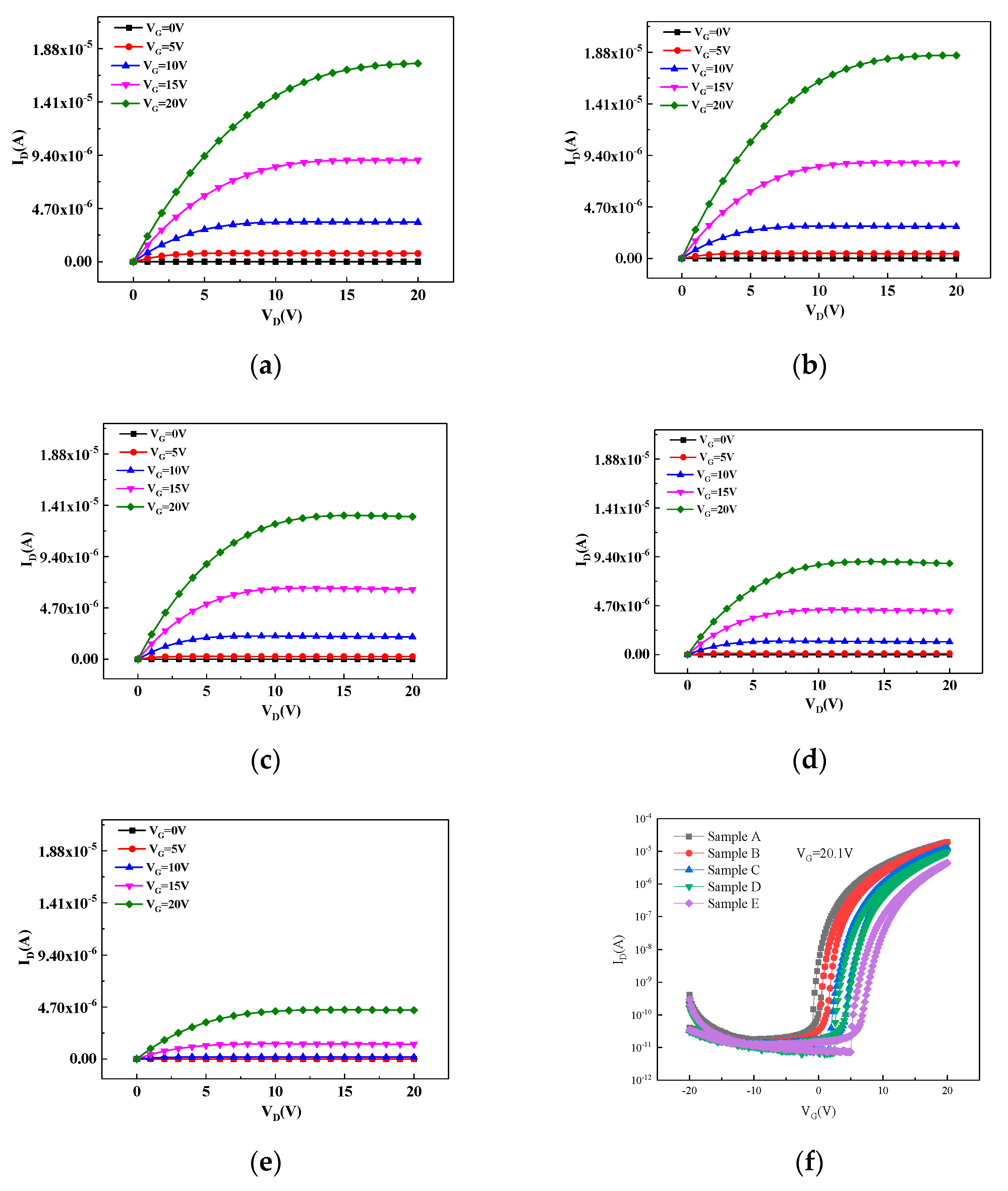
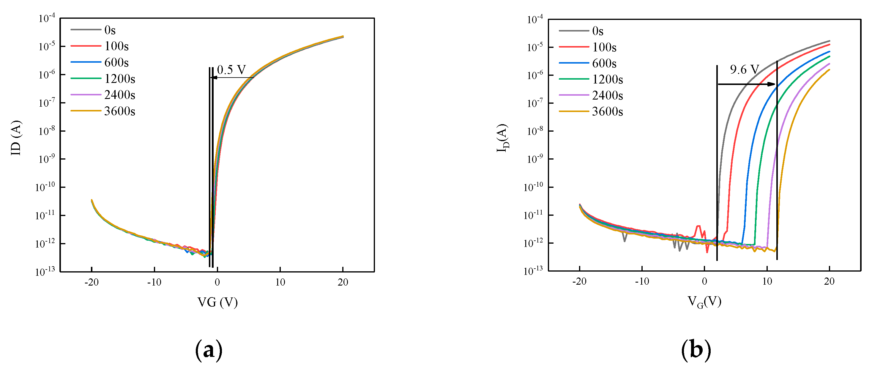
3. Results and Discussion
4. Conclusions
Author Contributions
Funding
Acknowledgments
Conflicts of Interest
References
- Eda, G.; Fanchini, G.; Chhowalla, M. Large-area ultrathin films of reduced graphene oxide as a transparent and flexible electronic material. Nat. Nanotechnol. 2008, 3, 270–274. [Google Scholar] [CrossRef] [PubMed]
- Lin, C.L.; Chen, F.H.; Hung, C.C.; Chen, P.S.; Deng, M.Y.; Lu, C.M.; Huang, T.H. New a-IGZO Pixel Circuit Composed of Three Transistors and One Capacitor for Use in High-Speed-Scan AMOLED Displays. J. Disp. Technol. 2015, 11, 1031–1034. [Google Scholar]
- Kim, Y.H.; Heo, J.S.; Kim, T.H.; Park, S.; Yoon, M.H.; Kim, J.; Oh, M.S.; Yi, G.R.; Noh, Y.Y.; Park, S.K. Flexible metal-oxide devices made by room-temperature photochemical activation of sol–gel films. Nature 2012, 489, 128–132. [Google Scholar] [CrossRef] [PubMed]
- Nomura, K.; Ohta, H.; Takagi, A.; Kamiya, T.; Hirano, M.; Hosono, H. Room-temperature fabrication of transparent flexible thin-film transistors using amorphous oxide semiconductors. Nature 2004, 432, 488–492. [Google Scholar] [CrossRef] [PubMed]
- Rim, Y.S.; Kim, D.L.; Jeong, W.H.; Kim, H.J. Effect of Zr addition on ZnSnO thin-film transistors using a solution process. Appl. Phys. Lett. 2010, 97, 233502. [Google Scholar] [CrossRef]
- Jiang, Q.; Feng, L.; Wu, C.; Sun, R.; Li, X.; Lu, B.; Ye, Z.; Lu, J. Amorphous ZnAlSnO thin-film transistors by a combustion solution process for future displays. Appl. Phys. Lett. 2015, 106, 053503. [Google Scholar] [CrossRef]
- Chiang, H.Q.; Wager, J.F.; Hoffman, R.L.; Jeong, J.; Keszler, D.A. High mobility transparent thin-film transistors with amorphous zinc tin oxide channel layer. Appl. Phys. Lett. 2005, 86, 013503. [Google Scholar] [CrossRef]
- Jackson, W.B.; Hoffman, R.L.; Herman, G.S. High-performance flexible zinc tin oxide field-effect transistors. Appl. Phys. Lett. 2005, 87, 193503. [Google Scholar] [CrossRef]
- Fortunato, E.M.C.; Pereira, L.M.N.; Barquinha, P.M.C.; Botelho Do Rego, A.M.; Gogmzalves, G.; Vil, A.; Morante, J.R.; Martins, R.F.P. High mobility indium free amorphous oxide thin film transistors. Appl. Phys. Lett. 2008, 92, 222103. [Google Scholar]
- Ogo, Y.; Nomura, K.; Yanagi, H.; Kamiya, T.; Hirano, M.; Hosono, H. Tin monoxide as an s-orbital-based p-type oxide semiconductor: Electronic structures and TFT application. Phys. Status Solidi 2009, 206, 2187–2191. [Google Scholar] [CrossRef]
- Kim, K.A.; Bak, J.Y.; Choi, J.S.; Yoon, S.M. Solution-processed semiconducting aluminum-zinc-tin-oxide thin films and their thin-film transistor applications. Ceram. Int. 2014, 40, 7829–7836. [Google Scholar] [CrossRef]
- Cho, D.H.; Yang, S.; Byun, C.; Shin, J.; Ryu, M.K.; Park, S.H.K.; Hwang, C.S.; Chung, S.M.; Cheong, W.S.; Yoon, S.M.; et al. Transparent Al–Zn–Sn–O thin film transistors prepared at low temperature. Appl. Phys. Lett. 2008, 93, 142111. [Google Scholar] [CrossRef]
- Nose, M.; Zhou, M.; Nagae, T.; Mae, T.; Yokota, M.; Saji, S. Properties of Zr–Si–N coatings prepared by RF reactive sputtering. Surf. Coat. Technol. 2000, 132, 163–168. [Google Scholar] [CrossRef]
- Ohtsu, Y.; Egami, M.; Fujita, H.; Yukimura, K. Preparation of zirconium oxide thin film using inductively coupled oxygen plasma sputtering. Surf. Coat. Technol. 2005, 196, 81–84. [Google Scholar] [CrossRef]
- Mattogno, G.; Righini, G.; Montesperelli, G.; Traversa, E. XPS analysis of the interface of ceramic thin films for humidity sensors. Appl. Surf. Sci. 1993, 70, 363–366. [Google Scholar] [CrossRef]
- Kim, H.R.; Choi, K.I.; Lee, J.H.; Akbar, S.A. Highly sensitive and ultra-fast responding gas sensors using self-assembled hierarchical SnO2 spheres. Sens. Actuators B Chem. 2009, 136, 138–143. [Google Scholar] [CrossRef]
- Xu, J.; Chang, Y.; Zhang, Y.; Ma, S.; Qu, Y.; Xu, C. Effect of silver ions on the structure of ZnO and photocatalytic performance of Ag/ZnO composites. Appl. Surf. Sci. 2008, 255, 1996–1999. [Google Scholar] [CrossRef]
- Jeon, J.K.; Um, J.G.; Lee, S.; Jang, J. Control of O-H bonds at a-IGZO/SiO2 interface by long time thermal annealing for highly stable oxide TFT. AIP Adv. 2017, 7, 125110. [Google Scholar] [CrossRef]
- Ning, H.; Liu, X.; Xu, H.; Lu, K.; Zhang, H.; Zhang, X.; Yao, R.; Fang, Z.; Wang, X.; Peng, J. A study of contact properties between molybdenum and amorphous silicon tin oxide thin film transistors. J. Soc. Inf. Disp. 2018, 26, 681–686. [Google Scholar] [CrossRef]
- Razak, A.F.; Devadason, S.; Sanjeeviraja, C.; Swaminathan, V. Effect of annealing on structural and optical properties of ZnO thin films by sol gel technique. Chalcogenide Lett. 2011, 8, 511–519. [Google Scholar]
- Kim, J.; Hosono, H. Development of Ultra-Wide Bandgap Amorphous Oxide Semiconductors for Future Electronics; Meeting Abstracts; The Electrochemical Society: Pennington, NJ, USA, 2018; p. 1205. [Google Scholar]
- Mo, Y.G.; Kim, M.; Kang, C.K.; Jeong, J.H.; Park, Y.S.; Choi, C.G.; Kim, H.D.; Kim, S.S. Amorphous-oxide TFT backplane for large-sized AMOLED TVs. J. Soc. Inf. Disp. 2011, 19, 1. [Google Scholar] [CrossRef]
- Chen, A.; Zhu, K.; Zhong, H.; Shao, Q.; Ge, G. A new investigation of oxygen flow influence on ITO thin films by magnetron sputtering. Sol. Energy Mater. Sol. Cells 2014, 120, 157–162. [Google Scholar] [CrossRef]
- Yasuno, S.; Kita, T.; Morita, S.; Kugimiya, T.; Hayashi, K.; Sumie, S. Transient photoconductivity responses in amorphous In-Ga-Zn-O films. J. Appl. Phys. 2012, 112, 53715. [Google Scholar] [CrossRef]
- Liu, X.; Chen, J.; Fang, Z.; Ning, H.L.; Hu, S.; Tao, R.; Zeng, Y.; Zheng, Z.; Yao, R.; Lan, L.; et al. A novel nondestructive testing method for amorphous Si–Sn–O films. J. Phys. D Appl. Phys. 2016, 49, 505102. [Google Scholar] [CrossRef]


| Sample A | Sample B | Sample C | Sample D | Sample E | |
|---|---|---|---|---|---|
| Power of ZrO2 (W) | 15 | 15 | 25 | 35 | 45 |
| Power of AZTO (W) | 120 | 100 | 100 | 100 | 100 |
| Sample A | Sample B | Sample C | Sample D | Sample E | |
|---|---|---|---|---|---|
| Peak of Al 2p3/2 (eV) | 73.53 | 73.55 | 73.60 | 73.60 | 73.59 |
| Peak of Sn 3d5/2 (eV) | 486.60 | 486.60 | 486.60 | 486.58 | 486.59 |
| Peak of Zn 2p3/2 (eV) | 1021.61 | 1021.62 | 1021.63 | 1021.59 | 1021.59 |
| Sample A | Sample B | Sample C | Sample D | Sample E | |
|---|---|---|---|---|---|
| Density by XRR (g/cm3) | 5.97 ± 0.02 | 5.85 ± 0.12 | 5.84 ± 0.15 | 5.88 ± 0.09 | 5.90 ± 0.10 |
| Thickness by XRR (nm) | 20.2 ± 0.1 | 20.6 ± 0.1 | 20.6 ± 0.1 | 20.7 ± 0.1 | 20.8 ± 0.1 |
| Roughness by XRR(nm) | 0.96 ± 0.04 | 1.12 ± 0.03 | 1.16 ± 0.12 | 1.10 ± 0.10 | 1.09 ± 0.04 |
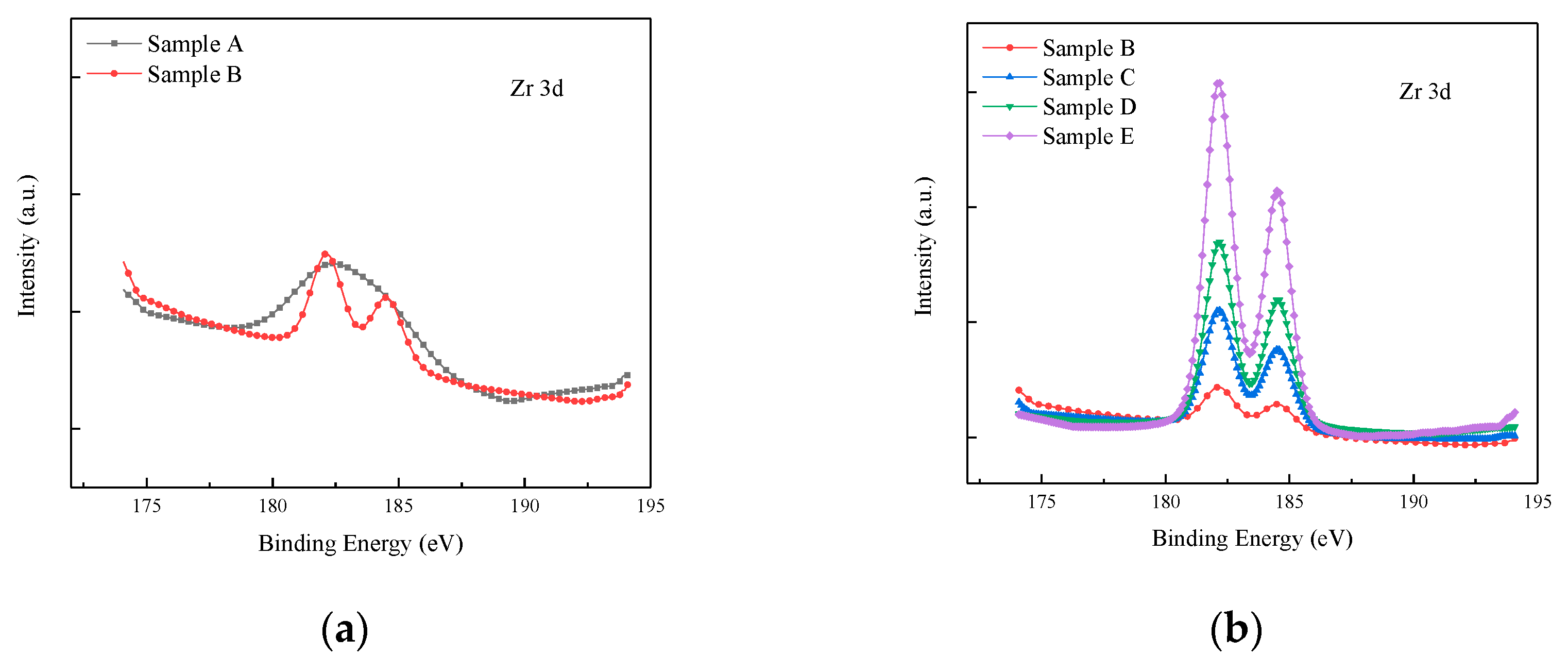
| Zr content (at.%) | 0.34 ± 0.01 | 0.63 ± 0.01 | 1.00 ± 0.01 | 1.78 ± 0.01 | 2.79 ± 0.01 |
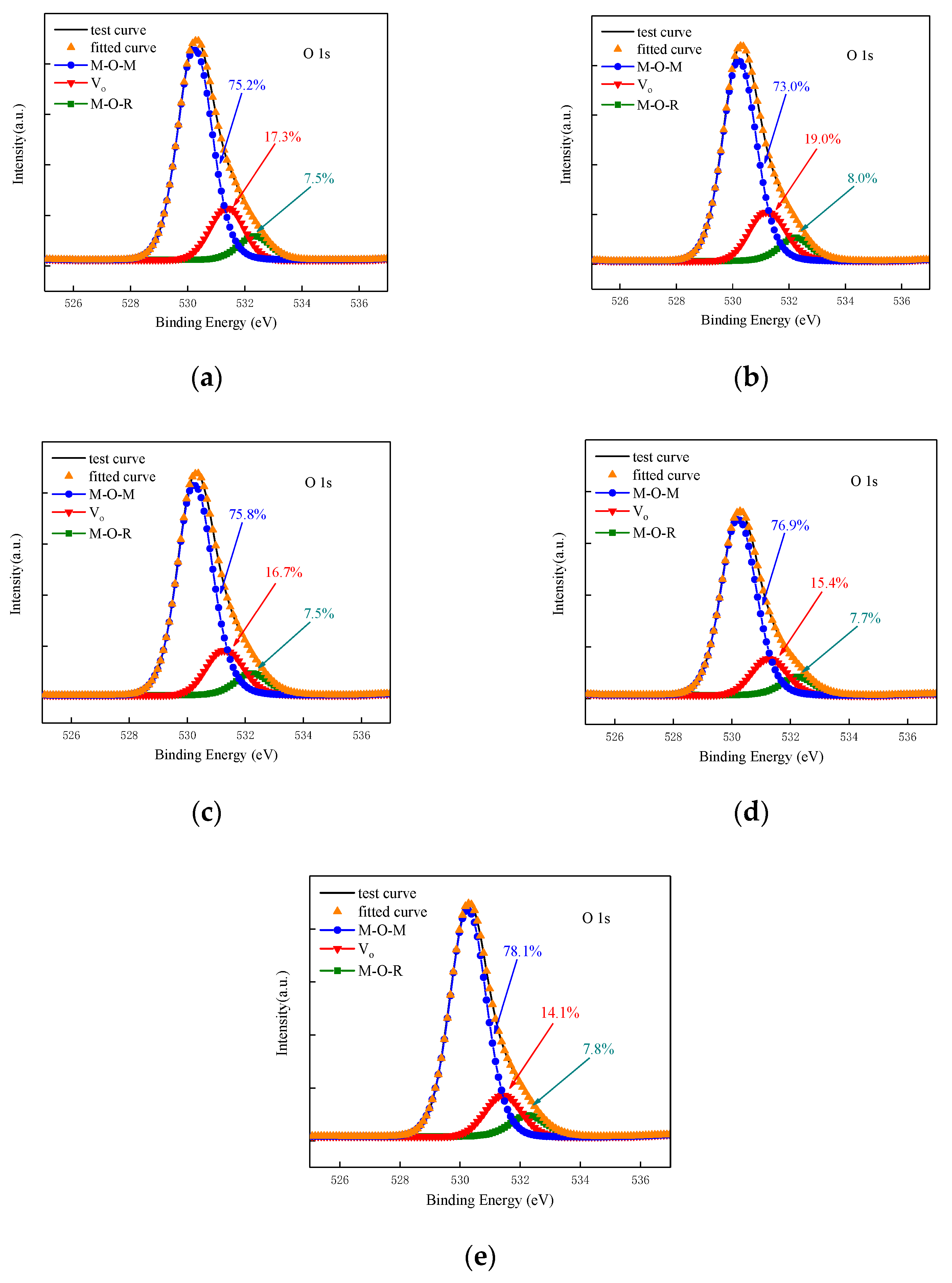
| Svo/Sall (%) | 17.3 ± 0.8 | 19.0 ± 0.1 | 16.0 ± 0.7 | 15.4 ± 0.6 | 14.1 ± 0.1 |
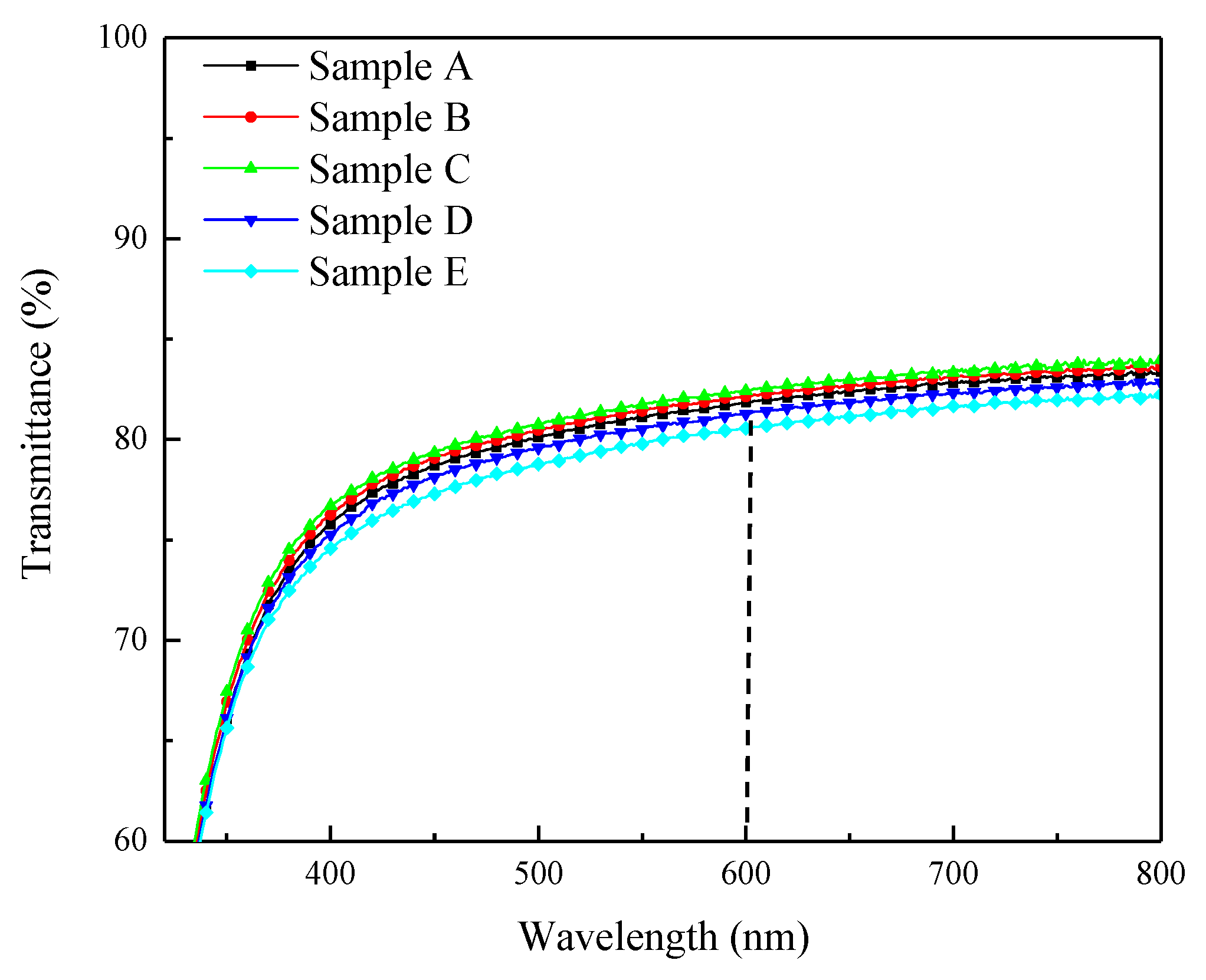
| Transmittance at 600 nm (%) | 81.8 | 82.1 | 82.4 | 81.3 | 80.6 |
| RMS roughness (nm) | 0.446 | 0.402 | 0.387 | 0.399 | 0.490 |
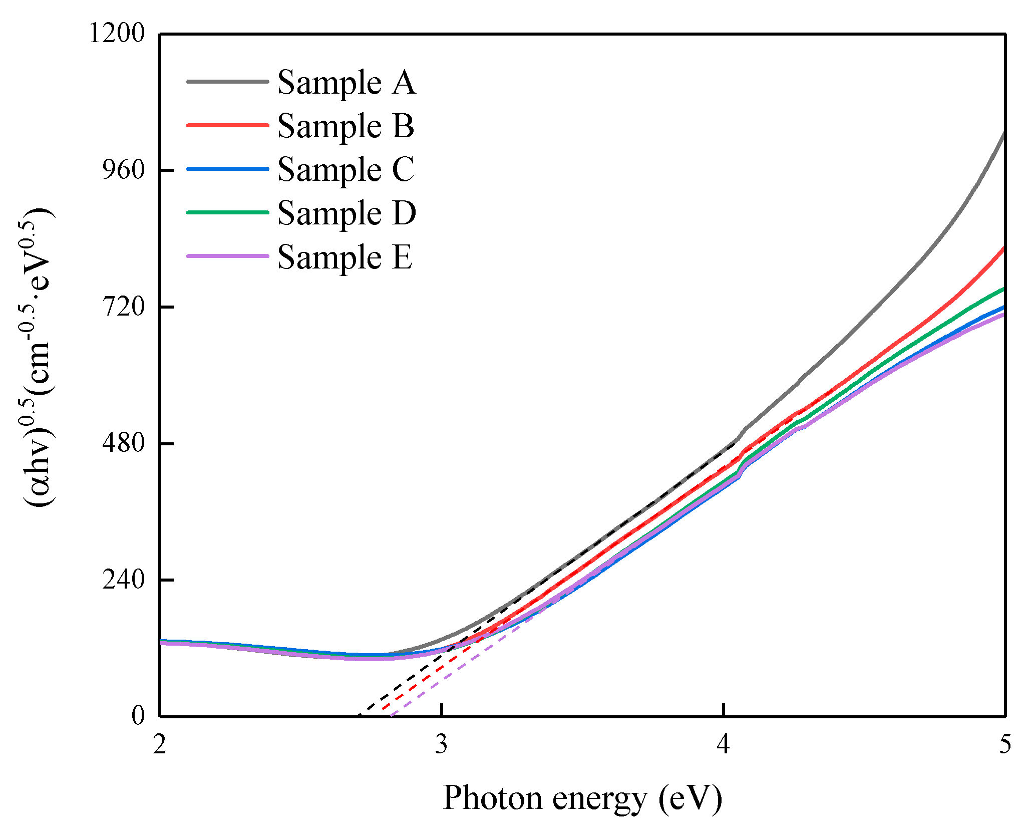
| Optical band gap (eV) | 2.71 | 2.76 | 2.86 | 2.86 | 2.86 |
| μ-PCD mean peak (mV) | 114.1 | 139.3 | 110.8 | 95.8 | 80.9 |
| μ-PCD D value | 1.24 | 1.54 | 1.35 | 0.77 | 0.77 |
| Sample A | Sample B | Sample C | Sample D | Sample E | |
|---|---|---|---|---|---|
| μsat (cm2/(V∙S)) | 7.1 ± 0.1 | 8.0 ± 0.6 | 7.6 ± 0.6 | 7.3 ± 0.3 | 5.2 ± 0.6 |
| Ion/Ioff | (1.86 ± 0.20) × 106 | (2.01 ± 0.34) × 106 | (1.66 ± 0.16) × 106 | (1.45 ± 0.27) × 106 | (8.89 ± 2.77) × 105 |
| SS (V/dec) | 0.23 ± 0.02 | 0.18 ± 0.03 | 0.25 ± 0.05 | 0.29 ± 0.05 | 0.27 ± 0.02 |
| Von (V) | −0.22 ± 0.12 | 1.08 ± 0.20 | 2.41 ± 0.14 | 3.04 ± 0.18 | 5.45 ± 0.11 |
© 2019 by the authors. Licensee MDPI, Basel, Switzerland. This article is an open access article distributed under the terms and conditions of the Creative Commons Attribution (CC BY) license (http://creativecommons.org/licenses/by/4.0/).
Share and Cite
Zhang, X.; Liu, X.; Lu, K.; Ning, H.; Guo, D.; Wang, Y.; Li, Z.; Shi, M.; Yao, R.; Peng, J. The Performance of Zr-Doped Al-Zn-Sn-O Thin Film Transistor Prepared by Co-Sputtering. Appl. Sci. 2019, 9, 5150. https://doi.org/10.3390/app9235150
Zhang X, Liu X, Lu K, Ning H, Guo D, Wang Y, Li Z, Shi M, Yao R, Peng J. The Performance of Zr-Doped Al-Zn-Sn-O Thin Film Transistor Prepared by Co-Sputtering. Applied Sciences. 2019; 9(23):5150. https://doi.org/10.3390/app9235150
Chicago/Turabian StyleZhang, Xiaochen, Xianzhe Liu, Kuankuan Lu, Honglong Ning, Dong Guo, Yiping Wang, Zhihang Li, Muyang Shi, Rihui Yao, and Junbiao Peng. 2019. "The Performance of Zr-Doped Al-Zn-Sn-O Thin Film Transistor Prepared by Co-Sputtering" Applied Sciences 9, no. 23: 5150. https://doi.org/10.3390/app9235150