O-Band and C/L-Band III-V Quantum Dot Lasers Monolithically Grown on Ge and Si Substrate
by
Qi Feng
1,2, 
Wenqi Wei
1,3,
Bin Zhang
1,3,
Hailing Wang
1,3,
Jianhuan Wang
1,3,
Hui Cong
1,
Ting Wang
1,2,3,4,* and
Jianjun Zhang
1,2,3,4,* 1
Beijing National Laboratory for Condensed Matter Physics and Institute of Physics, Chinese Academy of Sciences, Beijing 100190, China
2
Center of Materials Science and Optoelectronics Engineering, University of Chinese Academy of Sciences, Beijing 100049, China
3
School of Physical Sciences, University of Chinese Academy of Sciences, Beijing 100190, China
4
Songshan Lake Materials Laboratory, Dongguan 523808, Guangdong, China
*
Authors to whom correspondence should be addressed.
Appl. Sci. 2019, 9(3), 385; https://doi.org/10.3390/app9030385
Submission received: 7 December 2018
/
Revised: 12 January 2019
/
Accepted: 14 January 2019
/
Published: 23 January 2019
(This article belongs to the Special Issue Silicon Photonics – Emerging Devices and Applications)
Abstract
:Featured Application
optical communication, silicon photonics.
Abstract
Direct epitaxial growth of III-V heterostructure on CMOS-compatible silicon wafer offers substantial manufacturing cost and scalability advantages. Quantum dot (QD) devices are less sensitive to defect and temperature, which makes epitaxially grown III-V QD lasers on Si one of the most promising technologies for achieving low-cost, scalable integration with silicon photonics. The major challenges are that heteroepitaxial growth of III-V materials on Si normally encounters high densities of mismatch dislocations, antiphase boundaries and thermal cracks, which limit the device performance and lifetime. This paper reviews some of the recent developments on hybrid InAs/GaAs QD growth on Ge substrates and highly uniform (111)-faceted hollow Si (001) substrates by molecular beam epitaxy (MBE). By implementing step-graded epitaxial growth techniques, the emission wavelength can be tuned into either an O band or C/L band. Furthermore, microcavity QD laser devices are fabricated and characterized. The epitaxially grown III-V/IV hybrid platform paves the way to provide a promising approach for future on-chip silicon photonic integration.
1. Introduction
Over the past few years, III-V-based photonic materials and devices have attracted much attention in the silicon photonics research fields [1,2,3,4,5,6,7,8]. For the large-scale integration of complex optoelectronic circuits, on-chip light source could potentially achieve a higher integration density with a compact size and provide a better performance due to its economic advantages and energy efficiency [4,5,9,10,11,12]. Due to the rapid growth of cloud-based application and data centers, the demand for high capacity and compact optical links is significantly increasing. Despite the tremendous progress towards silicon photonic integration with building blocks including modulators, detectors, waveguides, and multiplexers/de-multiplexers, an efficient, reliable and electrically-pumped laser on a silicon substrate has been the major challenge [7,8,13,14,15,16,17,18,19,20,21,22]. Advances have been made in group-IV-based light emitters widely used in integrated circuits, such as Si Raman lasers, germanium-on-Si lasers and GeSn-on-Si lasers [23,24,25,26]; however, due to the indirect bandgap of group IV materials, they do not emit light efficiently. Therefore, the integration of other light-emitting materials is highly demanded for silicon photonic integrated circuits. Due to the inherent limitations of Group IV materials for gain, modulation and detection at near-infrared wavelengths, in the foreseeable future, by combining the existing silicon photonics techniques with the outstanding optical properties of III-V materials, the hybridization of group III-V and IV materials would be very promising to boost the performances of photonics integration [9,27]. The direct epitaxial growth of III-V materials on Si substrates is considered as one of the most promising methods to provide Si-based lasers for future photonics integration. Furthermore, after being extensively investigated for decades, silicon photonics is going beyond a technology that is purely communication-oriented and has evolved into a versatile integration platform, which also has great potential in various application fields but not limited to sensing, signal processing, quantum sciences, microwave engineering, imaging, spectroscopy, and high-performance computing [28,29,30,31,32,33].
The monolithic integration of III-V materials on an Si platform have been investigated for decades [34,35]. Unfortunately, monolithic III-V-on-Si integration poses critical issues stemming from the large material dissimilarity between III-V and group IV materials, including the formation of antiphase boundaries (APBs), threading dislocations (TDs) and the creation of thermal cracks. When polar III-V materials grow on non-polar Si substrates, anti-phase boundaries form; these boundaries are electrically charged planar defects and act as non-radiative recombination centers for optoelectronic devices and electronics devices, leading to the performance degradation. The 4% (7.5%) lattice mismatch between GaAs (InP) and Si makes direct growth of high-quality GaAs (InP) on Si very difficult, resulting in high dislocation densities on the order of (>109–1010 cm−2). In addition, the difference in the coefficient of thermal expansion between III-V and IV materials could promote the accumulation of thermal stress, which then leads to thermal micro-cracks in the epilayer while the wafer is cooled down from the growth temperature to room temperature (RT).
There have been many researches carried out on the monolithic growth of InAs/GaAs quantum-dot (QD) lasers on Si substrates in the last few years, including techniques such as offcut Si (001) substrates, Ge/Si virtual substrates, hydrogen annealing process, intermediate GaP buffer, and V-grooved Si substrates [36,37,38,39,40,41,42,43,44,45,46,47,48,49,50,51]. However, most of the above techniques suffer from high defect density and thermal mismatch-induced material degradation. In addition, most of experimental results reported so far are referring to the 1.3 μm wavelength at the O-band telecom window [41,42,44,45,49,52,53,54,55,56,57,58,59,60,61,62,63]. Most of the works intentionally utilized offcut silicon substrates to suppress antiphase disorder arising from the interface between III-V (polar) and silicon (non-polar). Otherwise, patterned (001) silicon substrate or InP was utilized in the heterostructures. For the C-band or L-band telecom window, there are very few works that have been reported [50,64]. Since many of the Si photonic passive and active devices are based on C-band applications, III-V light sources on Si in the long-wavelength range are becoming strongly demanded. Especially, for future Si photonic integration, Si-based high-gain III-V semiconductor optical amplifiers (SOAs) for long-haul transmission at the C/L-band are also essential components as on-chip replacements for erbium-doped fiber amplifier (EDFA). Here, we reviewed some of recent works of III-V/Si hybrid materials and devices at both O-band and C/L-band telecom windows, via a novel (111)-faceted silicon hollow structure which is capable of suppressing both APBs and thermal cracks simultaneously.
2. O-Band and C/L-Band III-V Quantum Dot Devices via III-V/IV Hybrid Growth
As previously stated, APDs are planar defects and debilitate device performance; they are known to be electrically active and can be detrimental for laser diode efficiency [65]. For conventional III-V devices, any threading dislocation or APDs propagating through the active layers will act as a non-radiative recombination center, leading to an increased threshold current density for III-V lasers on Ge or Si substrates [36]. Therefore, most QD lasers were grown on offcut Si substrate to avoid the formation of APDs. An alternative method is to grow GaAs on Si with an intermediate Ge epitaxial layer, which offers a near-GaAs on Si lattice constant but has a few defects. This is because the lattice mismatch between Ge and GaAs is very small, only a 0.08% mismatch. Since the realization of a quantum dot laser diode on miscut Ge substrate was reported by Huiyun Liu et al. [36], extensive investigation of the monolithic growth of III-V materials on a group IV platform has been carried out. Their novel growth method shows great promise of the ideal virtual substrate of Ge substrates and Ge/Si substrates for subsequent epitaxially grown III-V materials, thus promoting the development of III-V quantum dot lasers. In 2012, with the initial GaAs nucleation layer at the proper growth temperature, the InAs/GaAs quantum dots grown on a Ge substrate were realized [37,66]. This was an essential step towards the monolithic integration of III-V QD lasers on Si substrates by using Ge-on-Si substrate. In addition, the room temperature threshold current density of 64.3 A/cm2 has been reported. Then, the dislocation filter layer was introduced to improve the 1.3 μm emission [40,41,67]. InAlAs/GaAs and InGaAs/GaAs strained-layer superlattice (SLSs) structures were used to reduce the density of TDs generated at the interface between III-V buffer layer and the IV substrate, and it was found that InAlAs is more effective than InGaAs/GaAs SLSs in suppressing the propagation of TDs. Further reduction of density of TDs was then achieved by additional elevated temperature steps (annealing) during the growth of InAs/GaAs QD structures on Si substrates [47]. The annealing process also results in significant improvements in optical properties and laser device performance. These attempts have been carried out upon Si or Ge substrates with 4 or 6 degrees offcut to the [110] direction. However, the GaAs buffer layers on these structures are at least 1 μm thick, which renders the height difficulty for subsequent fabrication and integration. Therefore, a novel method in which only a thinner buffer layer is required would be more promising for future on-chip silicon photonic integration.
2.1. C/L-Band InAs Quantum Dots on Ge Substrate
Recently, we achieved monolithic growth of III-V on Ge miscut substrate by only using a 250-nm-thick GaAs buffer layer through the formation of a double atomic layer which could reduce the TDs [68]. In addition, as previously stated, most of the work so far has referred to the 1.3 μm wavelength at the O-band telecom window. Few work regarding the emission at the C/L-band telecom window has been reported to date [50,64]. Long wavelength III-V light sources on Si substrates at 1550 nm or C/L-band have become strongly demanded, since most of the Si-based photonic passive and active devices are based on applications at the C-band window. Furthermore, QD lasers emitting at 1550 nm benefit from the low loss transmission in mid/long-haul communications. To extend the emission wavelength from O-band to C/L-band for incoming silicon photonic integration, the step-graded epitaxial growth method was developed.
The InAs/In0.25Ga0.75As QD structure was grown by solid-source MBE on Ge (001) substrate with 2° offcut toward [110] direction. The formation of a double atomic layer at the Ge surface is essential for the subsequent III-V material growth, because the APDs would form while growing polar III-V materials on a non-polar germanium substrate. The cross-sectional scanning transmission electron microscopy (STEM) of the complete epitaxial III-V quantum dot structure is shown in Figure 1a. The growth direction of the structure is shown as a white arrow in Figure 1a. Firstly, before epitaxial growth, the Ge substrate is de-oxidized at 450 °C for 15 min. Then an ultra-thin 60 nm layer of Ge buffer is deposited on the Ge substrate followed by an in-situ annealing to create the double atomic layer of Ge for the subsequent III-V material growth. APD free surface can be obtained then by migration-enhanced epitaxy (MEE) of the GaAs nucleation layer and two-step GaAs growth of 20 nm and 230 nm at 450 °C and 560 °C, respectively. Therefore, for photonics integration, only an ultra-thin GaAs buffer layer of 250 nm thick which is APD free was deposited, in comparison with the work stated previously, in which at least a 1-μm-thick buffer layer for III-V QD structure growth is required [68]. Furthermore, as reported in our previous work [68,69], with the step-graded epitaxial growth method, the InGaAs metamorphic buffer layer with the thickness of 700 nm is grown on top of the GaAs buffer layer. To suppress the propagation of misfit dislocations, the low growth temperature of 380 °C was used for the InGaAs metamorphic layer. Here, the InGaAs metamorphic buffer consists of two layers: a 200 nm step-graded InGaAs layer from In0.09Ga0.91As to In0.13Ga0.87As, followed by a 200 nm In0.13Ga0.87As and a 200 nm step-graded InGaAs from In0.13Ga0.87As to In0.25Ga0.75As, followed by a 100 nm In0.25Ga0.75As layer at 380 °C and 500 °C, respectively. Then, three periods of InAs QD layer grown on the In0.25Ga0.75As buffer layer form the active region. Each InAs QD layer consists of a 2.8 monolayer of InAs. They are capped by a 4 nm In0.25Ga0.75As spacer layer grown at an optimum temperature of 500 °C. Lastly, the surface InAs QDs are deposited with the same growth condition as the buried InAs QD layer for subsequent AFM characterization. More details of heterostructure growth can be found in Wenqi et al. [68].
As shown in Figure 1, the epitaxial structure is characterized using scanning transmission electron microscopy (STEM) on a focused ion beam (FIB) fabrication cross-sectional lamella. It is clear in Figure 1a that due to the usage of a 250-nm-thick APD-free ultra-thin GaAs buffer layer, there is no apparent defect propagation from the GaAs/Ge interface and InGaAs metamorphic buffer to the active layer. It indicates that the TDs have been significantly reduced. Figure 1b demonstrates the bright field TEM image of the interface between GaAs and Ge, where the low-density defects are mostly localized at the interface region without further propagation. A high-magnification STEM image of InAs quantum dots is shown in Figure 1c, indicating the defect-free active layers. In addition, due to intermixing during the growth of InAlAs capping layer as reported in Ge/Si system [70], the InAs QDs are truncated. It shows that a 250-nm-thick ultra-thin GaAs buffer layer on the double-atomic layer of Ge can effectively act as a APD-free substrate for the subsequent monolithic growth of a III-V quantum dot laser structure. Furthermore, with the step-graded index method, the emission wavelength can be successfully extended to 1550 nm.
2.2. O-Band and C/L-Band InAs/GaAs Quantum Dots on (111)-Faceted Si Hollow Substrate
Most reported studies of III-V QD lasers were grown on 2–6° offcut Ge or Si towards [110] substrates to prevent the formation of APDs [36,37,38,39,40,41,42,43,45,46,66,67]. Unfortunately, offcut Ge or Si substrates are not fully compatible with standard CMOS processing foundries, and it may hinder the viability of InAs QD lasers as light emitters for silicon photonics. In addition, it would be more attractive to realize a laser in which the intermediate germanium layer is not required. Because the germanium layer restricts the application range of silicon circuits and due to the large optical absorption coefficient at the telecommunications window, it is difficult to realize the light coupling between germanium with silicon waveguide. Therefore, a high-performance III-V laser directly grown on a silicon substrate is considered a more promising solution for silicon photonic–electronic integration.
To date, various approaches have been carried out to tackle the challenges associated with material incompatibility, including the large mismatch of lattice constants and thermal expansion coefficients and the polar–nonpolar nature of the III-V/IV semiconductor system. The novel epitaxy approach to integrate GaAs on silicon relies on aspect ratio trapping (ART) of defects in narrow oxide trenches to suppress the threading dislocations. The misfit strain by the formation of twinned stacking faults (SFs) is relaxed through using the V-groove structure [49,50,51,60,64,71,72]. This method stands out for its capability in defect trapping, good controllability and high compatibility with the Si CMOS process. Recently, Key May Lau et al., found out that III-V materials including QD lasers and in-plane GaAs nanowires can be monolithically grown by MBE upon GaAs-on-V-groove patterned Si substrates which are prepared by metal oxide chemical vapor deposition (MOCVD) [49,60,71]. Although APDs are avoided by the grooves and most dislocations are confined to the interface, there is still no way to release the thermal mismatch. In addition, 1550 nm quantum dot diode lasers have been realized on CMOS-standard (001) silicon substrate, but with a very thick GaAs intermediate buffer layer of 2.2 μm [64]. Therefore, a novel method is strongly demanded to improve the laser structure for the reduction of thermal mismatch, for less TDs and better laser performance.
Recently, by using U-shaped patterned Si (001) substrates, we obtained (111)-faceted-sawtooth Si hollow structures by homo-epitaxy [69]. The in-situ hybrid epitaxy of InAs/GaAs on such Si substrates can be realized to achieve highly efficient 1300 nm and 1550 nm emission by using a dual chamber MBE. As shown in Figure 2a, the U-shaped patterns are fabricated by a standard process on standard 8-inch on-axis Si (001) substrate, by using a SiO2 hard mask, deep ultraviolet (DUV) lithography, dry etch, and removal of SiO2 in diluted hydrofluoric acid (HF) solution. The U-shaped patterns have a period of 360 nm with a ridge width of 140 nm and a depth of approximately 500 nm. After cleaving into 32 mm × 32 mm dies and ex-situ chemical cleaning, the samples are loaded into the SiGe MBE chamber for growth. After 550 nm Si growth, the (111)-faceted sawtooth hollow structures are obtained, as shown in Figure 2b, which can be used for a subsequent in-situ GaAs buffer layer and III-V QD laser structure growth. The formation of the hollow structure in Si can partially reduce the thermal mismatch between the epitaxial GaAs layer and Si substrate. By reducing the period of the U shape structures in the initial Si (001) substrate, we may achieve a (111)-faceted sawtooth structure by depositing a thinner Si buffer layer. The entire epi-structure for GaAs buffer growth on Si is schematically shown in Figure 2c.
A 10 nm AlAs nucleation layer was grown prior to the buffer layer growth on the (111)-faceted sawtooth hollow Si (001) substrate, and it significantly reduced the anti-phase boundary density at the III-V/Si interface due to the higher bonding energy of AlAs [39,46]. The 600-nm thick GaAs buffer layers were then grown using a two-step method to flatten the sawtooth structure-induced geometric unevenness. An APD-free surface can be obtained then by migration-enhanced epitaxy (MEE) of the GaAs nucleation layer and two-step GaAs growth of 40 nm and 560 nm at 380 °C and 580 °C, respectively. In0.15Ga0.85As/InAs quantum wells as dislocation filter layers (DFLs) were grown on a flattened surface with 200-nm GaAs spacing layers in-between to effectively reduce the dislocation density, followed by active QD layer growth. The separation GaAs layer was grown at 480 oC, and the DFLs consisted of five periods of 10 nm In0.15Ga0.85As/10 nm GaAs. To further reduce the threading dislocation density (TDD), an additional two periods of In0.15Al0.85As/GaAs DFLs were utilized, which consisted of five-periods of 10 nm In0.15Al0.85As/10 nm GaAs strained layers separated by 200 nm GaAs. Finally, five periods of GaAs/AlGaAs superlattices (SLs) separated by a 50 nm GaAs spacing layer were deposited at 580 °C to achieve a smooth GaAs surface for the flattening process. Each SL has 10 periods of 2 nm GaAs/ 2 nm Al0.6Ga0.4As alternating structures, followed by a 200 nm GaAs grown at 560 °C [69]. For O-band light emission, a standard five-layer InAs/GaAs dot-in-a-well (DWELL) structure was grown on this GaAs/Si substrate. Each DWELL layer consisted of a 3.1 monolayer InAs QD layer sandwiched by a 2-nm In0.14Ga0.86As wetting layer and a 6-nm In0.14Al0.86As capping layer. The DWELLs were separated by a 50-nm GaAs spacing layer, which was grown at 560 °C. For the C/L-band emission of InAs QDs, step-graded metamorphic InGaAs buffer layers were introduced as previously presented [68]. Thermal cycle annealing was utilized to further improve the flatness and quality of InGaAs layers. The active region consists of three periods of InAs QD layers grown at 450 °C. Each of the InAs QDs layers consists of 3.1 monolayer InAs capped by a 4-nm In0.3Ga0.7As layer and separated by a 45-nm In0.3Ga0.7As spacing layer grown at 500 °C. Further details of InAs/GaAs QD growth can be found in References [68,69]. Cross-sectional TEM measurements were carried out to characterize the crystalline quality of the active regions. Figure 3a,b shows defection-free and high-quality DWELL structures for both samples, with insets illustrating the high resolution TEM images of individual InAs QDs. As presented above, a step-graded InGaAs metamorphic buffer was inserted to obtain InAs/InGaAs QDs with an emission wavelength extended to 1550 nm on a GaAs/Si (001) substrate. In addition, as shown in the insets, the size of QD increases for the C/L-band active region.
In order to verify the influence of (111)-faceted-sawtooth Si (001) hollow structure on defect suppression at the GaAs/Si interface, surface SEM images of identical GaAs structures directly grown on a (111)-faceted Si and standard Si are compared here, as shown in Figure 4a,b, respectively. The images of the atomic force microscope (AFM) with the scanning area of 2 μm × 2 μm are shown in Figure 4c,d. It is clear that a high quality GaAs buffer layer with a root-mean-square (RMS) roughness of approximately 0.4 nm can be obtained on (111)-faceted-sawtooth hollow Si (001) substrates, comparing with the rough surface for the InAs QDs structure on a standard Si (001) substrate. The great surface flatness and low defect density are contributed to by the designed (111)-faceted Si hollow structure. The Si (111) facets can effectively annihilate the APDs generated at the GaAs/Si interface by simply changing the propagating direction of Ga-Ga and As-As APDs from a vertical direction to 54.74 °C. Therefore, the generated APDs can join and annihilate within 30 nm from the interface, which effectively reduce the propagating defects into the upper structures. By applying this technique, a high quality GaAs surface can be created as shown in Figure 4, that leads to an essential platform for the hybridization of a III-V photonic structure on Si substrates.
Photoluminescence (PL) measurements were carried out for O-band InAs/GaAs and C-band InAs/InGaAs QDs on (111)-faceted-hollow Si (001) substrates, as shown in Figure 5. InAs/GaAs QDs on GaAs substrate were grown as a reference sample to compare with that grown on the Si substrate. A high quality QDs on Si substrate was confirmed by the FWHM of 36 meV in PL emission for InAs/GaAs QDs on Si (001). It is shown in Figure 5a that PL peak intensity is approximately 25% higher for InAs/GaAs QDs on Si than that on the GaAs substrate. This is due to the enhanced pump power from the grating-like (111)-faceted Si substrate. The experimental result is verified by measuring the surface reflectivity of the grating structure at the wavelength of 1300 nm, which gives a value of approximately 55%. In comparison, the GaAs on the offcut Si substrate exhibits a surface reflection of only 33%. Therefore, it can be concluded that the enhanced PL peak intensity is induced from the increased reflection from Si grating structures. This further confirms a high-quality GaAs layer on Si (001). As shown in Figure 5b, the PL intensity of the C/L-band InAs/InGaAs QDs is approximately one order of magnitude lower than that of O-band InAs/GaAs QDs. This is because the carrier confinement of the InAs/InGaAs structure is weaker than that of the standard InAs/GaAs QD structure.
Similar photoluminescence intensity to that on the GaAs substrate is observed. Moreover, a metamorphic InGaAs buffer layer is utilized to extend the emission wavelength of InAs QDs to the C/L band on GaAs/Si (001) substrates. Strong 1550 nm light emission is realized in the absence of an intermediate layer or any InP-based material systems. With such a technique, highly efficient and integrated O-band and C/L-band InAs/(In)GaAs QD lasers on the Si (001) substrate are expected in the near future.
3. InAs QD Microcavity Lasers on (111)-Faceted Hollow Si (001) Substrate
In order to verify the material quality of InAs/GaAs QDs on the Si substrate, one method of rapid feedback is to fabricate optically-pumped microcavity lasers. The optically-pumped microcavity lasers exhibit advantages of a small footprint (μm scale) and ultra-low lasing threshold in comparison with conventional Fabry Perot lasers. Here, two types of microcavity lasers on Si are demonstrated, which are microcavity lasers and microdisk lasers. The fabrication and experimental details are discussed as below.
3.1. Optically-Pumped QD Micropillar Laser on Si Substrate
Optically-pumped InAs/GaAs quantum-dot micropillar laser on an exact Si (001) by a (111)-faceted Si hollow structure has been achieved through the standard fabrication process, including photolithography and dry etch. By calculation, the distributed Bragg reflectors (DBRs) and an active layer with specific thicknesses have been grown on an ultra-flat GaAs/Si (001) substrate. The cross-sectional SEM image of the whole structure is shown in Figure 6a. The DBRs consist of 33.5 bottom and 15 top pairs of alternating quarter-wavelength thick GaAs/AlAs layers, which are 94.2 nm GaAs and 111.1 nm AlAs, respectively. They were grown at an optimum temperature of 610 °C and 560 °C. The active layer in the center of one wavelength-thick GaAs cavity is sandwiched between the top and bottom DBRs. The active layer contains five periods of InAs/GaAs dot-in-a-well (DWELLs) structures, each of which consists of a 3.1 monolayer InAs QD layer sandwiched by a 2 nm In0.143Ga0.857As wetting layer and 6 nm In0.143Al0.857As capping layer. With only 250 nm GaAs buffer layer grown on (111)-faceted sawtooth hollow Si (001) substrate, subsequent DFLs can be deposited and followed by micropillar laser structures consisting of DBRs and an active layer. The QD micropillar laser structures on Si(001) were fabricated with diameters ranging from 15 to 250 μm, as shown in Figure 6b. Figure 6c shows the tilted SEM view of the micropillar laser, indicating high quality of the sidewall.
A micro-PL system with a continuous wave (cw) pump laser at 532 nm was used to characterize the laser operation of InAs QD micropillar cavities on Si (001). The laser characteristics (L-L curves) of InAs QD micropillar laser on Si substrate with a mesa diameter of 15 μm is shown in Figure 7a. By linear fitting the L-L curve, the laser threshold pump power is approximately calculated to be 20 μW. Figure 7b shows the plot of integrated PL intensity of InAs QDs micropillar with increasing pump power at different operating temperatures ranging from 20 to 100 °C. During the experiment, the red-shift of laser emission wavelength is observed with increasing operation temperature by approximately 0.165 nm/°C. The results indicate the great temperature stability of InAs/GaAs QD microcavity lasers on Si (001) hollow structure as a potential platform for III-V optoelectronic devices on standard Si (001) substrates. With reduced density of InAs QDs, such a structure can also be implemented as a silicon-based single photon source for quantum information applications.
3.2. InAs QD Microdisk Laser on Si Substrate
Furthermore, InAs/GaAs quantum-dot microcavity laser on exact Si (001) via (111)-faceted Si hollow structure has been demonstrated. By using a (111)-faceted Si (001) hollow substrate, GaAs buffer and dislocation filter layer were epitaxially grown to reduce the threading dislocations in the subsequent QD laser structure’s growth. The active layer consisting of five periods of InAs/GaAs dot-in-a-well (DWELLs) structure was sandwiched between Al0.35Ga0.65As claddings with a 600-nm-thick Al0.65Ga0.35As sacrificial layer. The structural characterization of the QD active layer has been presented in earlier work [69]. The schematic diagram and corresponding SEM image of the laser structure are shown in Figure 8. The microdisk size of 4 μm is chosen for laser characterization. The L-L characterization of Si-based microdisk laser is shown in Figure 9, with a threshold pump power of approximately 380 μW, which is similar to those on the GaAs substrate. The inset of Figure 9 shows the log–log plot of the L-L curve, revealing an ‘S-shaped’ nonlinear transition.
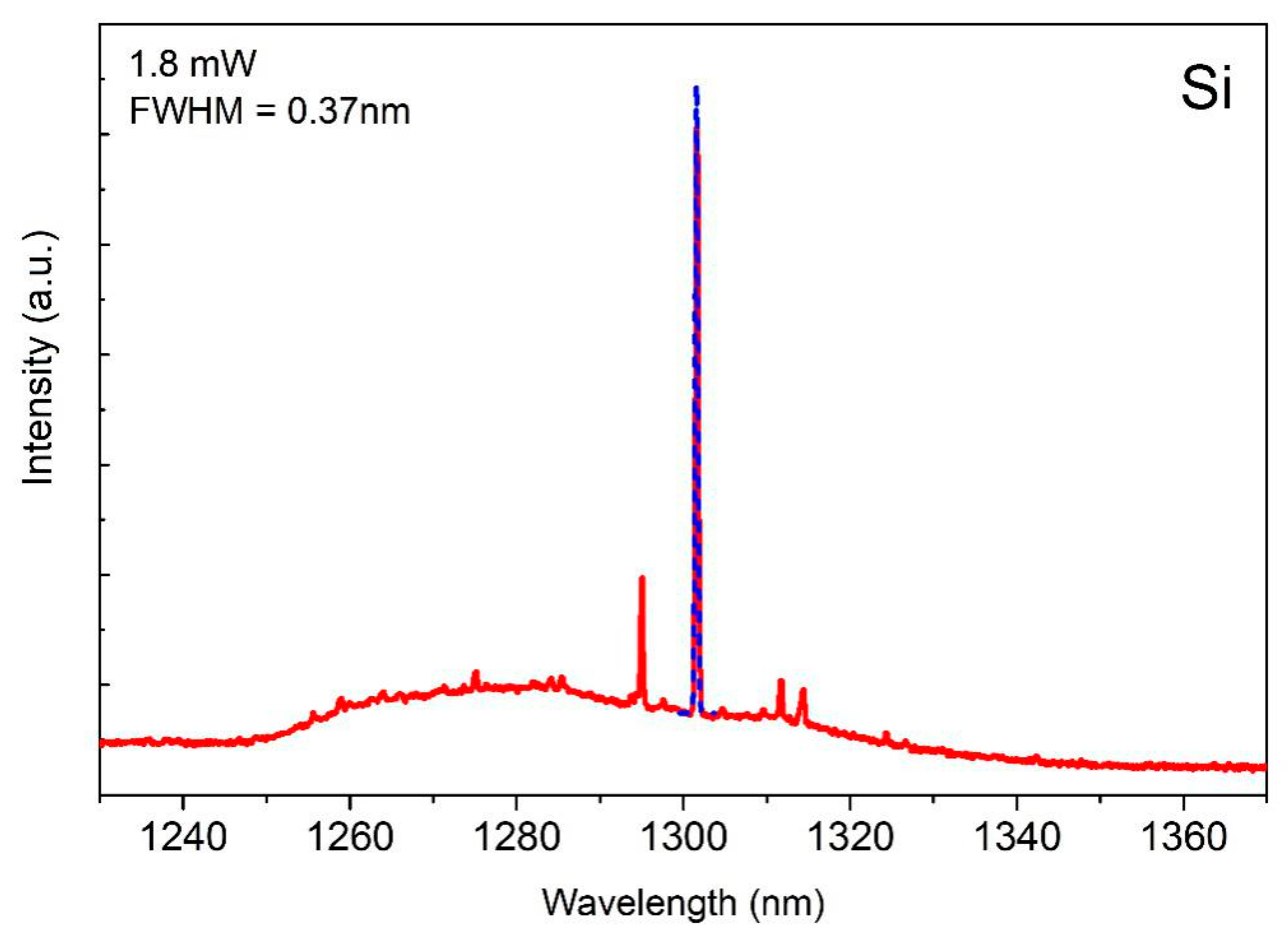
Figure 10 shows the emission spectrum under an optical pump power of 1.8 mW for an O-band InAs/GaAs QD microdisk laser. The laser spectrum shows a full-width-half-maximum (FWHM) of 0.37 nm, which indicates a cold cavity quality factor (Q) of 3645. The spacing between the adjacent modes in the same radial order agrees well with the calculated free spectral range (18 nm) for the first-order mode of the microdisk laser. The QD microcavity laser on the CMOS-compatible Si (001) substrate could potentially be implemented in the application of low-power integrated light sources in the near future.
4. Conclusions
We have reviewed rthe ecent progress in InAs QD lasers on on-axis Si (001) substrates via hybrid epitaxial growth techniques. Here, this technique presents a promising approach (Si sawtooth hollow structure) of migrating III-V photonic devices on to an Si platform for future laser-on-Si integration. This paves the way for large-scale silicon photonic integration, which consequently boosts the data transmission density in telecommunication. The future development of such techniques could potentially benefit the applications of optical interconnects, sensing and even compact LIDAR chips.
Author Contributions
Conceptualization, Q.F., W.W., T.W.; Methodology, W.W., B.Z.; Resources, Q.F., W.W., B.Z., H.W., J.W., H.C.; Writing-Original Draft Preparation, Q.F.; Writing-Review & Editing, Q.F., T.W., J.Z. Supervision, T.W., J.Z. Funding Acquisition, T.W.
Funding
This research was funded by National Natural Science Foundation of China (Grant Nos. 11504415, 11434010, 11574356, 61804177, 11804382 and 61635011), the National Key Research and Development Program of China (Nos. 2016YFA0300600, 2016YFA0301700, and 2015CB932400), and the Key Research Program of Frontier Sciences, CAS (Grant No. QYZDB-SSW-JSC009). Ting Wang was supported by the Youth Innovation Promotion Association of CAS (No. 2018011).
Conflicts of Interest
The authors declare no conflict of interest.
References
- Liu, A.Y.; Srinivasan, S.; Norman, J.; Gossard, A.C.; Bowers, J.E. Quantum dot lasers for silicon photonics. Photonic Res. 2015, 3, B1–B9. [Google Scholar] [CrossRef]
- Zhou, Z.; Yin, B.; Michel, J. On-chip light sources for silicon photonics. Light Sci. Appl. 2015, 4, e358. [Google Scholar] [CrossRef]
- Wang, Z.; Abbasi, A.; Dave, U.; Groote, A.; Kumari, S.; Kunert, B.; Merckling, C.; Pantouvaki, M.; Shi, Y.; Tian, B.; et al. Novel Light Source Integration Approaches for Silicon Photonics. Laser Photonics Rev. 2017, 11, 1700063. [Google Scholar] [CrossRef] [Green Version]
- Chen, X.; Li, C.; Tsang, H.K. Device engineering for silicon photonics. NPG Asia Mater. 2011, 3, 34. [Google Scholar] [CrossRef]
- Rickman, A. The commercialization of silicon photonics. Nat. Photonics 2014, 8, 579–582. [Google Scholar] [CrossRef]
- David, T.; Aaron, Z.; John, E.B.; Tin, K.; Graham, T.R.; Laurent, V.; Delphine, M.-M.; Eric, C.; Léopold, V.; Jean-Marc, F.; et al. Roadmap on silicon photonics. J. Opt. 2016, 18, 073003. [Google Scholar] [Green Version]
- Malka, D.; Cohen, E.; Zalevsky, Z. Design of 4 × 1 Power Beam Combiner Based on MultiCore Photonic Crystal Fiber. Appl. Sci. 2017, 7, 695. [Google Scholar] [CrossRef]
- Sintov, Y.; Malka, D.; Zalevsky, Z. Prospects for diode-pumped alkali-atom-based hollow-core photonic-crystal fiber lasers. Opt. Lett. 2014, 39, 4655–4658. [Google Scholar] [CrossRef]
- Mi, Z.; Yang, J.; Bhattacharya, P.; Qin, G.; Ma, Z. High-Performance Quantum Dot Lasers and Integrated Optoelectronics on Si. Proc. IEEE 2009, 97, 1239–1249. [Google Scholar] [CrossRef]
- Sugawara, M.; Usami, M. Handling the heat. Nat. Photonics 2009, 3, 30–31. [Google Scholar] [CrossRef]
- Asghari, M.; Krishnamoorthy, A.V. Energy-efficient communication. Nat. Photonics 2011, 5, 268–270. [Google Scholar] [CrossRef]
- Heck, M.J.R.; Bowers, J.E. Energy Efficient and Energy Proportional Optical Interconnects for Multi-Core Processors: Driving the Need for On-Chip Sources. IEEE J. Sel. Top. Quantum Electron. 2014, 20, 332–343. [Google Scholar] [CrossRef]
- Reed, G.T.; Mashanovich, G.; Gardes, F.Y.; Thomson, D.J. Silicon optical modulators. Nat. Photonics 2010, 4, 518–526. [Google Scholar] [CrossRef] [Green Version]
- Xiao, X.; Xu, H.; Li, X.; Li, Z.; Chu, T.; Yu, Y.; Yu, J. High-speed, low-loss silicon Mach–Zehnder modulators with doping optimization. Opt. Express 2013, 21, 4116–4125. [Google Scholar] [CrossRef] [PubMed]
- Streshinsky, M.; Ding, R.; Liu, Y.; Novack, A.; Yang, Y.; Ma, Y.; Tu, X.; Chee, E.K.S.; Lim, A.E.-J.; Lo, P.G.-Q.; et al. Low power 50 Gb/s silicon traveling wave Mach-Zehnder modulator near 1300 nm. Opt. Express 2013, 21, 30350–30357. [Google Scholar] [CrossRef] [PubMed]
- Dosunmu, O.I.; Cannon, D.D.; Emsley, M.K.; Kimerling, L.C.; Unlu, M.S. High-speed resonant cavity enhanced Ge photodetectors on reflecting Si substrates for 1550-nm operation. IEEE Photonics Technol. Lett. 2005, 17, 175–177. [Google Scholar] [CrossRef]
- Yin, T.; Cohen, R.; Morse, M.M.; Sarid, G.; Chetrit, Y.; Rubin, D.; Paniccia, M.J. 31GHz Ge n-i-p waveguide photodetectors on Silicon-on-Insulator substrate. Opt. Express 2007, 15, 13965–13971. [Google Scholar] [CrossRef] [PubMed]
- Vivien, L.; Polzer, A.; Marris-Morini, D.; Osmond, J.; Hartmann, J.M.; Crozat, P.; Cassan, E.; Kopp, C.; Zimmermann, H.; Fédéli, J.M. Zero-bias 40Gbit/s germanium waveguide photodetector on silicon. Opt. Express 2012, 20, 1096–1101. [Google Scholar] [CrossRef]
- Bauters, J.F.; Davenport, M.L.; Heck, M.J.R.; Doylend, J.K.; Chen, A.; Fang, A.W.; Bowers, J.E. Silicon on ultra-low-loss waveguide photonic integration platform. Opt. Express 2013, 21, 544–555. [Google Scholar] [CrossRef] [Green Version]
- Heck, M.J.R.; Bauters, J.F.; Davenport, M.L.; Spencer, D.T.; Bowers, J.E. Ultra-low loss waveguide platform and its integration with silicon photonics. Laser Photonics Rev. 2014, 8, 667–686. [Google Scholar] [CrossRef]
- Zheng, X.; Shubin, I.; Li, G.; Pinguet, T.; Mekis, A.; Yao, J.; Thacker, H.; Luo, Y.; Costa, J.; Raj, K.; et al. A tunable 1x4 silicon CMOS photonic wavelength multiplexer/demultiplexer for dense optical interconnects. Opt. Express 2010, 18, 5151–5160. [Google Scholar] [CrossRef] [PubMed]
- Tan, D.T.H.; Ikeda, K.; Zamek, S.; Mizrahi, A.; Nezhad, M.P.; Krishnamoorthy, A.V.; Raj, K.; Cunningham, J.E.; Zheng, X.; Shubin, I.; et al. Wide bandwidth, low loss 1 by 4 wavelength division multiplexer on silicon for optical interconnects. Opt. Express 2011, 19, 2401–2409. [Google Scholar] [CrossRef]
- Liang, D.; Bowers, J.E. Recent progress in lasers on silicon. Nat. Photonics 2010, 4, 511–517. [Google Scholar] [CrossRef]
- Rong, H.; Liu, A.; Jones, R.; Cohen, O.; Hak, D.; Nicolaescu, R.; Fang, A.; Paniccia, M. An all-silicon Raman laser. Nature 2005, 433, 292–294. [Google Scholar] [CrossRef] [PubMed] [Green Version]
- Chang, H.-H.; Fang, A.W.; Sysak, M.N.; Park, H.; Jones, R.; Cohen, O.; Raday, O.; Paniccia, M.J.; Bowers, J.E. 1310nm silicon evanescent laser. Opt. Express 2007, 15, 11466–11471. [Google Scholar] [CrossRef] [PubMed]
- Wirths, S.; Geiger, R.; von den Driesch, N.; Mussler, G.; Stoica, T.; Mantl, S.; Ikonic, Z.; Luysberg, M.; Chiussi, S.; Hartmann, J.M.; et al. Lasing in direct-bandgap GeSn alloy grown on Si. Nat. Photonics 2015, 9, 88–92. [Google Scholar] [CrossRef] [Green Version]
- Yodo, T.; Tamura, M.; Saitoh, T. Relationship between the optical and structural properties in GaAs heteroepitaxial layers grown on Si substrates. J. Cryst. Growth 1994, 141, 331–342. [Google Scholar] [CrossRef]
- Subramanian, A.Z.; Ryckeboer, E.; Dhakal, A.; Peyskens, F.; Malik, A.; Kuyken, B.; Zhao, H.; Pathak, S.; Ruocco, A.; De Groote, A.; et al. Silicon and silicon nitride photonic circuits for spectroscopic sensing on-a-chip. Photonic Res. 2015, 3, B47–B59. [Google Scholar] [CrossRef]
- Bernhardt, B.; Ozawa, A.; Jacquet, P.; Jacquey, M.; Kobayashi, Y.; Udem, T.; Holzwarth, R.; Guelachvili, G.; Hänsch, T.W.; Picqué, N. Cavity-enhanced dual-comb spectroscopy. Nat. Photonics 2009, 4, 55–57. [Google Scholar] [CrossRef] [Green Version]
- Foster, M.A.; Salem, R.; Geraghty, D.F.; Turner-Foster, A.C.; Lipson, M.; Gaeta, A.L. Silicon-chip-based ultrafast optical oscilloscope. Nature 2008, 456, 81–84. [Google Scholar] [CrossRef]
- Silverstone, J.W.; Bonneau, D.; O’Brien, J.L.; Thompson, M.G. Silicon Quantum Photonics. IEEE J. Sel. Top. Quantum Electron. 2016, 22, 390–402. [Google Scholar] [CrossRef]
- Sun, J.; Timurdogan, E.; Yaacobi, A.; Hosseini, E.S.; Watts, M.R. Large-scale nanophotonic phased array. Nature 2013, 493, 195–199. [Google Scholar] [CrossRef] [PubMed]
- Hermans, M.; Burm, M.; Van Vaerenbergh, T.; Dambre, J.; Bienstman, P. Trainable hardware for dynamical computing using error backpropagation through physical media. Nat. Commun. 2015, 6, 6729. [Google Scholar] [CrossRef] [PubMed] [Green Version]
- Fischer, R.; Masselink, W.T.; Klem, J.; Henderson, T.; McGlinn, T.C.; Klein, M.V.; Morkoç, H.; Mazur, J.H.; Washburn, J. Growth and properties of GaAs/AlGaAs on nonpolar substrates using molecular beam epitaxy. J. Appl. Phys. 1985, 58, 374–381. [Google Scholar] [CrossRef]
- Mitsuru, S.; Hidefumi, M.; Yoshio, I.; Yoshihisa, S.; Masami, T. 1.5 µm-Long-Wavelength Multiple Quantum Well Laser on a Si Substrate. Jpn. J. Appl. Phys. 1991, 30, 3876–3878. [Google Scholar]
- Liu, H.Y.; Wang, T.; Jiang, Q.; Hogg, R.; Tutu, F.; Pozzi, F.; Seeds, A. Long-wavelength InAs/GaAs quantum-dot laser diode monolithically grown on Ge substrate. Nat. Photonics 2011, 5, 416–419. [Google Scholar] [CrossRef]
- Wang, T.; Lee, A.; Tutu, F.; Seeds, A.; Liu, H.; Jiang, Q.; Groom, K.; Hogg, R. The effect of growth temperature of GaAs nucleation layer on InAs/GaAs quantum dots monolithically grown on Ge substrates. Appl. Phys. Lett. 2012, 100, 052113. [Google Scholar] [CrossRef]
- Andrew, L.; Huiyun, L.; Alwyn, S. Semiconductor III–V lasers monolithically grown on Si substrates. Semicond. Sci. Technol. 2013, 28, 015027. [Google Scholar]
- Lee, A.D.; Jiang, Q.; Tang, M.; Zhang, Y.; Seeds, A.J.; Liu, H. InAs/GaAs Quantum-Dot Lasers Monolithically Grown on Si, Ge, and Ge-on-Si Substrates. IEEE J. Sel. Top. Quantum Electron. 2013, 19, 1901107. [Google Scholar] [CrossRef]
- Jiang, Q.; Tang, M.; Chen, S.; Wu, J.; Seeds, A.; Liu, H. InAs/GaAs quantum-dot superluminescent diodes monolithically grown on a Ge substrate. Opt. Express 2014, 22, 23242–23248. [Google Scholar] [CrossRef]
- Liu, A.Y.; Zhang, C.; Norman, J.; Snyder, A.; Lubyshev, D.; Fastenau, J.M.; Liu, A.W.K.; Gossard, A.C.; Bowers, J.E. High performance continuous wave 1.3 μm quantum dot lasers on silicon. Appl. Phys. Lett. 2014, 104, 041104. [Google Scholar] [CrossRef]
- Tang, M.; Chen, S.; Wu, J.; Jiang, Q.; Dorogan, V.G.; Benamara, M.; Mazur, Y.I.; Salamo, G.J.; Seeds, A.; Liu, H. 1.3-μm InAs/GaAs quantum-dot lasers monolithically grown on Si substrates using InAlAs/GaAs dislocation filter layers. Opt. Express 2014, 22, 11528–11535. [Google Scholar] [CrossRef]
- Chen, S.; Tang, M.; Wu, J.; Jiang, Q.; Dorogan, V.; Benamara, M.; Mazur, Y.; Salamo, G.; Liu, H. Long-Wavelength InAs/GaAs Quantum-Dot Light Emitting Sources Monolithically Grown on Si Substrate. Photonics 2015, 2, 646. [Google Scholar] [CrossRef]
- Mingchu, T.; Siming, C.; Jiang, W.; Qi, J.; Dongyoung, K.; Alwyn, S.; Huiyun, L. Optimisation of 1.3-μm InAs/GaAs Quantum-Dot Lasers Monolithically Grown on Si Substrates. J. Phys. Conf. Ser. 2015, 619, 012011. [Google Scholar]
- Tang, M.; Wu, J.; Chen, S.; Jiang, Q.; Seeds, A.J.; Liu, H.; Dorogan, V.G.; Benamara, M.; Mazur, Y.; Salamo, G. Optimisation of the dislocation filter layers in 1.3-μm InAs/GaAs quantum-dot lasers monolithically grown on Si substrates. IET Optoelectron. 2015, 9, 61–64. [Google Scholar] [CrossRef]
- Chen, S.; Li, W.; Wu, J.; Jiang, Q.; Tang, M.; Shutts, S.; Elliott, S.N.; Sobiesierski, A.; Seeds, A.J.; Ross, I.; et al. Electrically pumped continuous-wave III–V quantum dot lasers on silicon. Nat. Photonics 2016, 10, 307–311. [Google Scholar] [CrossRef] [Green Version]
- Orchard, J.R.; Shutts, S.; Sobiesierski, A.; Wu, J.; Tang, M.; Chen, S.; Jiang, Q.; Elliott, S.; Beanland, R.; Liu, H.; et al. In situ annealing enhancement of the optical properties and laser device performance of InAs quantum dots grown on Si substrates. Opt. Express 2016, 24, 6196–6202. [Google Scholar] [CrossRef]
- Chen, S.; Tang, M.; Wu, J.; Liao, M.; Seeds, A.; Liu, H. III-IV quantum dot lasers epitaxially grown on Si. In Proceedings of the 2017 Conference on Lasers and Electro-Optics Pacific Rim (CLEO-PR), Singapore, 31 July–4 August 2017; pp. 1–2. [Google Scholar]
- Tang, M.; Chen, S.; Wu, J.; Jiang, Q.; Kennedy, K.; Jurczak, P.; Liao, M.; Beanland, R.; Seeds, A.; Liu, H. Optimizations of Defect Filter Layers for 1.3-μm InAs/GaAs Quantum-Dot Lasers Monolithically Grown on Si Substrates. IEEE J. Sel. Top. Quantum Electron. 2016, 22, 50–56. [Google Scholar] [CrossRef]
- Shi, B.; Zhu, S.; Li, Q.; Wan, Y.; Hu, E.L.; Lau, K.M. Continuous-Wave Optically Pumped 1.55 μm InAs/InAlGaAs Quantum Dot Microdisk Lasers Epitaxially Grown on Silicon. ACS Photonics 2017, 4, 204–210. [Google Scholar] [CrossRef]
- Shi, B.; Li, Q.; Lau, K.M. Epitaxial growth of high quality InP on Si substrates: The role of InAs/InP quantum dots as effective dislocation filters. J. Appl. Phys. 2018, 123, 193104. [Google Scholar] [CrossRef] [Green Version]
- Wang, J.; Hu, H.; Yin, H.; Bai, Y.; Li, J.; Wei, X.; Liu, Y.; Huang, Y.; Ren, X.; Liu, H. 1.3 μm InAs/GaAs quantum dot lasers on silicon with GaInP upper cladding layers. Photonics Res. 2018, 6, 321–325. [Google Scholar] [CrossRef]
- Wan, Y.; Norman, J.; Li, Q.; Kennedy, M.J.; Liang, D.; Zhang, C.; Huang, D.; Zhang, Z.; Liu, A.Y.; Torres, A.; et al. 1.3 μm submilliamp threshold quantum dot micro-lasers on Si. Optica 2017, 4, 940–944. [Google Scholar] [CrossRef]
- Jhang, Y.-H.; Mochida, R.; Tanabe, K.; Takemasa, K.; Sugawara, M.; Iwamoto, S.; Arakawa, Y. Direct modulation of 1.3 μm quantum dot lasers on silicon at 60 °C. Opt. Express 2016, 24, 18428–18435. [Google Scholar] [CrossRef] [PubMed]
- Inoue, D.; Jung, D.; Norman, J.; Wan, Y.; Nishiyama, N.; Arai, S.; Gossard, A.C.; Bowers, J.E. Directly modulated 1.3 μm quantum dot lasers epitaxially grown on silicon. Opt. Express 2018, 26, 7022–7033. [Google Scholar] [CrossRef] [PubMed]
- Chen, S.; Liao, M.; Tang, M.; Wu, J.; Martin, M.; Baron, T.; Seeds, A.; Liu, H. Electrically pumped continuous-wave 1.3 μm InAs/GaAs quantum dot lasers monolithically grown on on-axis Si (001) substrates. Opt. Express 2017, 25, 4632–4639. [Google Scholar] [CrossRef] [PubMed]
- Liu, A.Y.; Peters, J.; Huang, X.; Jung, D.; Norman, J.; Lee, M.L.; Gossard, A.C.; Bowers, J.E. Electrically pumped continuous-wave 1.3 μm quantum-dot lasers epitaxially grown on on-axis (001) GaP/Si. Opt. Lett. 2017, 42, 338–341. [Google Scholar] [CrossRef]
- Jung, D.; Herrick, R.; Norman, J.; Jan, C.; Caranto, N.; Torres, A.; Wan, Y.; Gossard, A.C.; Bowers, J.E. Highly Improved Reliability of Low Threshold 1.3 μm III/V Quantum Dot Laser Epitaxially Grown on On-axis Si. In Proceedings of the Conference on Lasers and Electro-Optics, San Jose, CA, USA, 13–18 May 2018; p. SW3Q.2. [Google Scholar]
- Liu, H.Y.; Sellers, I.R.; Badcock, T.J.; Mowbray, D.J.; Skolnick, M.S.; Groom, K.M.; Gutiérrez, M.; Hopkinson, M.; Ng, J.S.; David, J.P.R.; et al. Improved performance of 1.3 μm multilayer InAs quantum-dot lasers using a high-growth-temperature GaAs spacer layer. Appl. Phys. Lett. 2004, 85, 704–706. [Google Scholar] [CrossRef]
- Wan, Y.; Li, Q.; Geng, Y.; Shi, B.; Lau, K.M. InAs/GaAs quantum dots on GaAs-on-V-grooved-Si substrate with high optical quality in the 1.3 μm band. Appl. Phys. Lett. 2015, 107, 081106. [Google Scholar] [CrossRef]
- Liao, M.; Chen, S.; Liu, Z.; Wang, Y.; Ponnampalam, L.; Zhou, Z.; Wu, J.; Tang, M.; Shutts, S.; Liu, Z.; et al. Low-noise 1.3 μm InAs/GaAs quantum dot laser monolithically grown on silicon. Photonics Res. 2018, 6, 1062–1066. [Google Scholar] [CrossRef]
- Wan, Y.; Li, Q.; Liu, A.Y.; Gossard, A.C.; Bowers, J.E.; Hu, E.L.; Lau, K.M. Optically pumped 1.3 μm room-temperature InAs quantum-dot micro-disk lasers directly grown on (001) silicon. Opt. Lett. 2016, 41, 1664–1667. [Google Scholar] [CrossRef]
- Liu, H.Y.; Hopkinson, M.; Harrison, C.N.; Steer, M.J.; Frith, R.; Sellers, I.R.; Mowbray, D.J.; Skolnick, M.S. Optimizing the growth of 1.3 μm InAs/InGaAs dots-in-a-well structure. J. Appl. Phys. 2003, 93, 2931–2936. [Google Scholar] [CrossRef]
- Zhu, S.; Shi, B.; Li, Q.; Lau, K.M. 1.5 μm quantum-dot diode lasers directly grown on CMOS-standard (001) silicon. Appl. Phys. Lett. 2018, 113, 221103. [Google Scholar] [CrossRef]
- Kroemer, H.; Polasko, K.J.; Wright, S.C. On the (110) orientation as the preferred orientation for the molecular beam epitaxial growth of GaAs on Ge, GaP on Si, and similar zincblende-on-diamond systems. Appl. Phys. Lett. 1980, 36, 763–765. [Google Scholar] [CrossRef]
- Lee, A.; Jiang, Q.; Tang, M.; Seeds, A.; Liu, H. Continuous-wave InAs/GaAs quantum-dot laser diodes monolithically grown on Si substrate with low threshold current densities. Opt. Express 2012, 20, 22181–22187. [Google Scholar] [CrossRef]
- Chen, S.; Tang, M.; Jiang, Q.; Wu, J.; Dorogan, V.G.; Benamara, M.; Mazur, Y.I.; Salamo, G.J.; Smowton, P.; Seeds, A.; et al. InAs/GaAs Quantum-Dot Superluminescent Light-Emitting Diode Monolithically Grown on a Si Substrate. ACS Photonics 2014, 1, 638–642. [Google Scholar] [CrossRef]
- Wei, W.-Q.; Wang, J.-H.; Gong, Y.; Shi, J.-A.; Gu, L.; Xu, H.-X.; Wang, T.; Zhang, J.-J. C/L-band emission of InAs QDs monolithically grown on Ge substrate. Opt. Mater. Express 2017, 7, 2955–2961. [Google Scholar] [CrossRef]
- Wei, W.-Q.; Wang, J.-H.; Zhang, B.; Zhang, J.-Y.; Wang, H.-L.; Feng, Q.; Xu, H.-X.; Wang, T.; Zhang, J.-J. InAs QDs on (111)-faceted Si (001) hollow substrates with strong emission at 1300 nm and 1550 nm. Appl. Phys. Lett. 2018, 113, 053107. [Google Scholar] [CrossRef]
- Zhang, J.J.; Rastelli, A.; Schmidt, O.G.; Bauer, G. Role of the wetting layer for the SiGe Stranski–Krastanow island growth on planar and pit-patterned substrates. Semicond. Sci. Technol. 2011, 26, 014028. [Google Scholar] [CrossRef]
- Li, Q.; Ng, K.W.; Lau, K.M. Growing antiphase-domain-free GaAs thin films out of highly ordered planar nanowire arrays on exact (001) silicon. Appl. Phys. Lett. 2015, 106, 072105. [Google Scholar] [CrossRef] [Green Version]
- Wan, Y.; Li, Q.; Liu, A.Y.; Gossard, A.C.; Bowers, J.E.; Hu, E.L.; Lau, K.M. Temperature characteristics of epitaxially grown InAs quantum dot micro-disk lasers on silicon for on-chip light sources. Appl. Phys. Lett. 2016, 109, 011104. [Google Scholar] [CrossRef] [Green Version]
Figure 1.
(a) The STEM image of C/L-band InAs quantum dots structure on Ge substrate. The white arrow: The growth direction of the epitaxial layers. (b) Bright field TEM image of GaAs/Ge interface. (c) High magnification STEM image of InAs QDs. The red-marked region: The cross section of a top-flattened InAs QD. All images are taken along [110] direction.
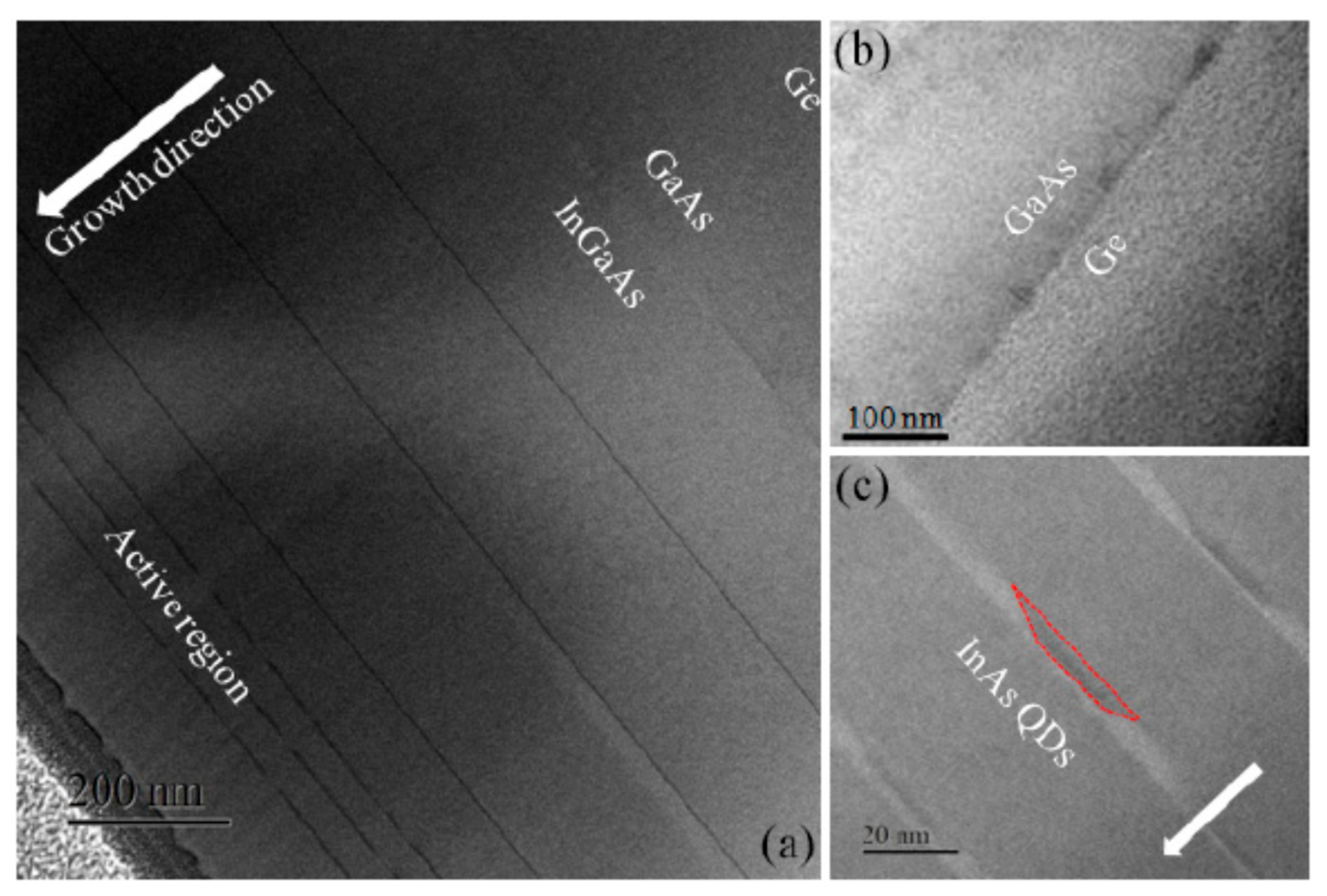
Figure 2.
(a) Cross-sectional scanning electron microscope image of U-shape Si (001) substrate, (b) (111)-faceted-sawtooth structure epitaxial growth on U-shape Si (001) hollow substrate, and (c) schematic diagram of epitaxial growth of (111)-faceted hollow structure on U-shape Si (001) substrate.
Figure 2.
(a) Cross-sectional scanning electron microscope image of U-shape Si (001) substrate, (b) (111)-faceted-sawtooth structure epitaxial growth on U-shape Si (001) hollow substrate, and (c) schematic diagram of epitaxial growth of (111)-faceted hollow structure on U-shape Si (001) substrate.

Figure 3.
(a) Cross-sectional TEM image of a five-layer InAs QDs grown on the sawtooth hollow structured Si (001) substrate for O-band emission. Inset: High resolution TEM image of an InAs/GaAs QD. (b) Cross-sectional TEM image of three-layer InAs QDs on the InGaAs/GaAs/Si (001) substrate for C/L-band emission. Inset: High resolution TEM image of a trapezoidal InAs/InGaAs QD.
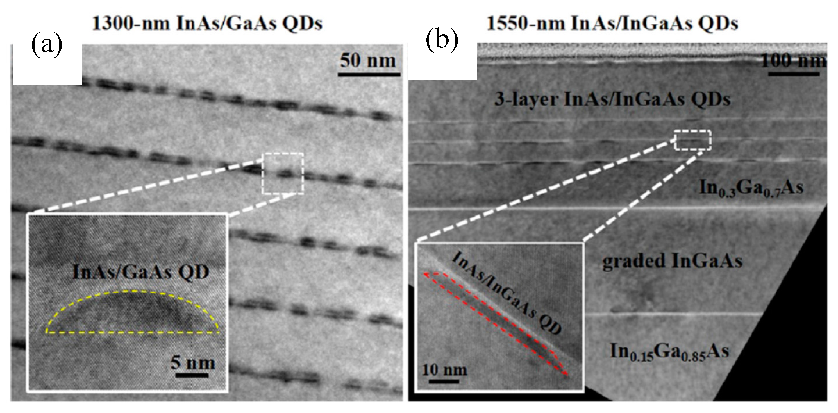
Figure 4.
Top-view SEM images of GaAs grown on (a) (111)-faceted sawtooth-structured Si (001) and (b) standard Si (001) substrates, and 2 μm × 2 μm atomic force microscope (AFM) images of GaAs film on (c) (111)-faceted Si (001) hollow structure and (d) GaAs/Si substrate.
Figure 4.
Top-view SEM images of GaAs grown on (a) (111)-faceted sawtooth-structured Si (001) and (b) standard Si (001) substrates, and 2 μm × 2 μm atomic force microscope (AFM) images of GaAs film on (c) (111)-faceted Si (001) hollow structure and (d) GaAs/Si substrate.
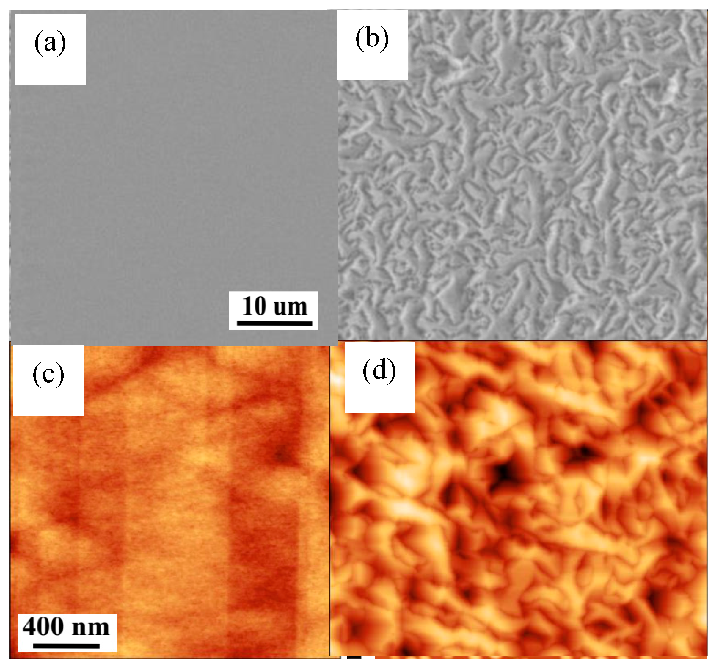
Figure 5.
Room temperature photoluminescence spectra of (a) InAs/GaAs QDs grown on GaAs and Si (001) substrates for O-band emission and (b) InAs/InGaAs QDs grown on Si (001) substrates for C/L-band emission. Insets: 1 μm × 1 μm AFM image of (a) InAs/GaAs QDs on Si and (b) InAs/InGaAs QDs on Si.
Figure 5.
Room temperature photoluminescence spectra of (a) InAs/GaAs QDs grown on GaAs and Si (001) substrates for O-band emission and (b) InAs/InGaAs QDs grown on Si (001) substrates for C/L-band emission. Insets: 1 μm × 1 μm AFM image of (a) InAs/GaAs QDs on Si and (b) InAs/InGaAs QDs on Si.
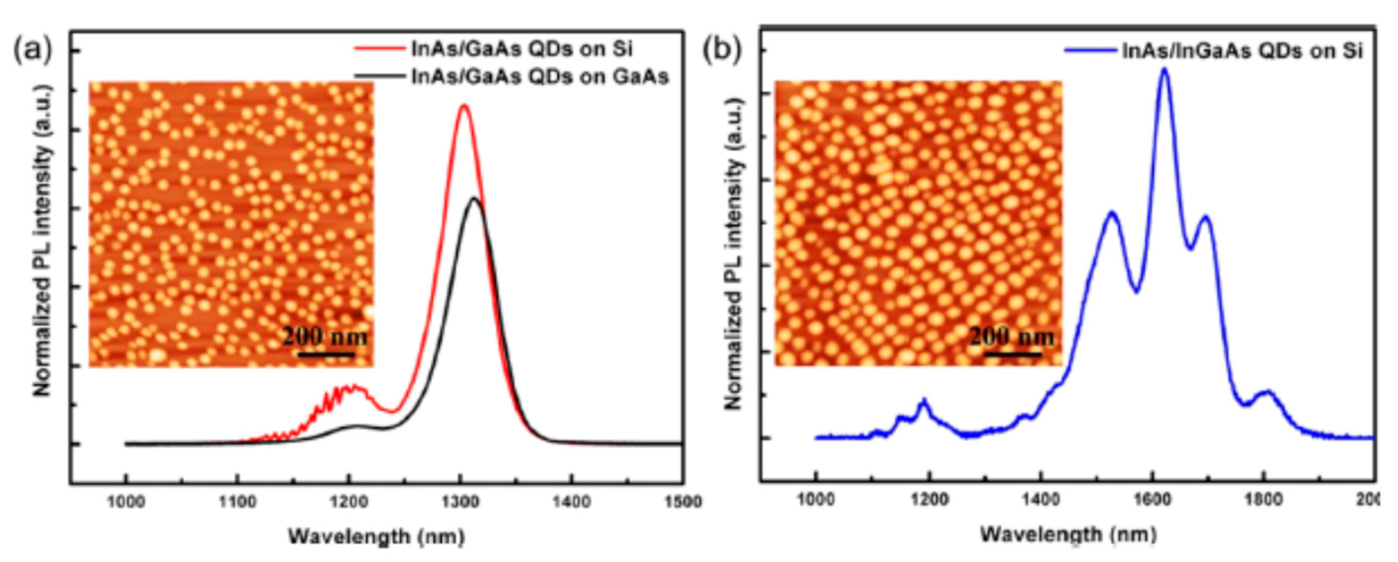
Figure 6.
(a) The cross-sectional SEM image of InAs/GaAs micropillar laser structure on (111)-faceted Si (001) hollow substrate; InAs/GaAs QDs embedded in one λ-cavity with 15 (33.5) pairs of top (bottom) DBRs; (b) top-view SEM image of micropillar lasers with different diameters; (c) tilted SEM image of InAs/GaAs QD micropillar laser on Si (001) with 15 μm diameter.
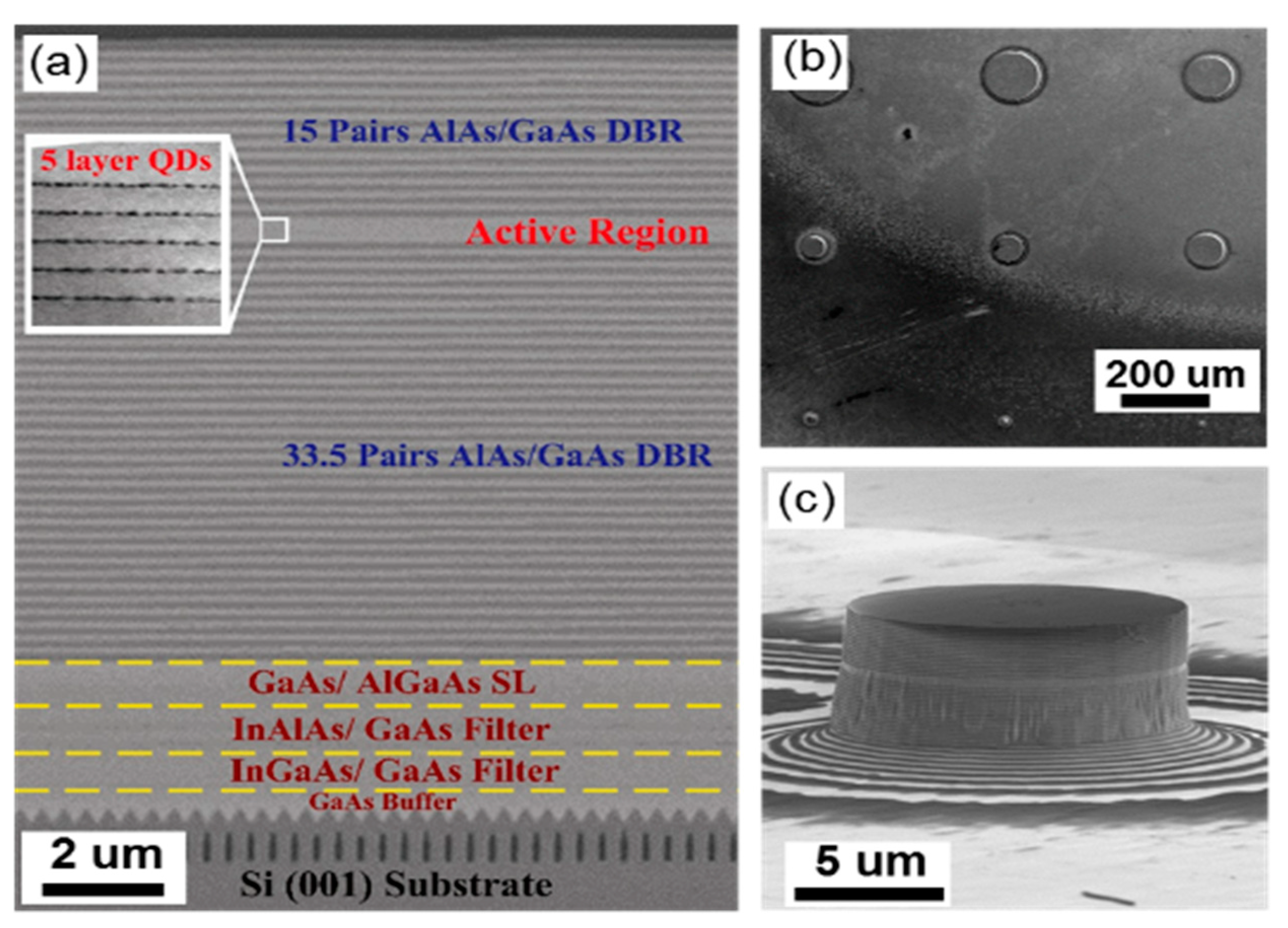
Figure 7.
(a) Output intensity as a function of pump power (L-L curve) of InAs/GaAs QD micropillar laser on Si at room temperature. Inset: spectral plot of micropillar laser at the pump power of 6 mW. (b) Integrated PL intensity of InAs QD micropillar on Si (001) as a function of pump power of temperature ranging from 20 to 100 °C.
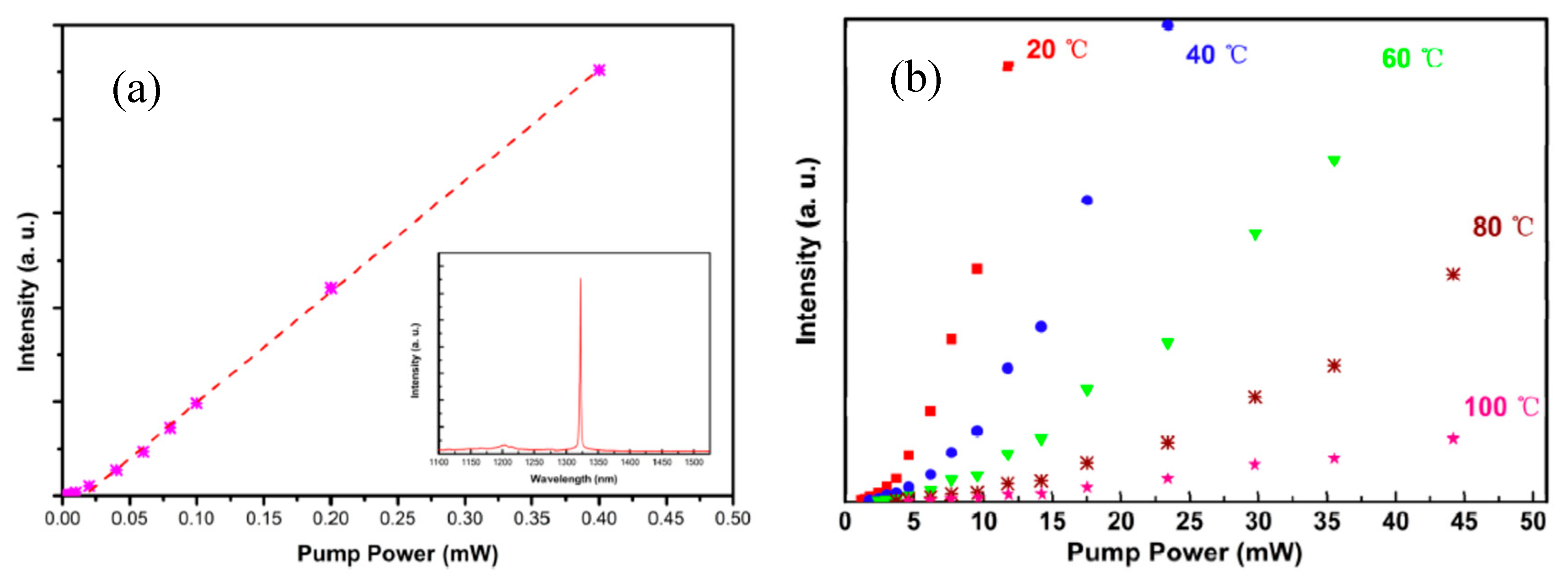
Figure 8.
Schematic diagram and SEM image of InAs QD microdisk laser structure.

Figure 9.
L-L curve of InAs/GaAs QD microdisk laser grown on (111)-faceted hollow Si (001) substrate; inset: double log plot of the S-curve.
Figure 9.
L-L curve of InAs/GaAs QD microdisk laser grown on (111)-faceted hollow Si (001) substrate; inset: double log plot of the S-curve.

Figure 10.
Laser spectrum for a 4 μm InAs/GaAs QD microdisk laser on Si.
© 2019 by the authors. Licensee MDPI, Basel, Switzerland. This article is an open access article distributed under the terms and conditions of the Creative Commons Attribution (CC BY) license (http://creativecommons.org/licenses/by/4.0/).
Share and Cite
MDPI and ACS Style
Feng, Q.; Wei, W.; Zhang, B.; Wang, H.; Wang, J.; Cong, H.; Wang, T.; Zhang, J. O-Band and C/L-Band III-V Quantum Dot Lasers Monolithically Grown on Ge and Si Substrate. Appl. Sci. 2019, 9, 385. https://doi.org/10.3390/app9030385
AMA Style
Feng Q, Wei W, Zhang B, Wang H, Wang J, Cong H, Wang T, Zhang J. O-Band and C/L-Band III-V Quantum Dot Lasers Monolithically Grown on Ge and Si Substrate. Applied Sciences. 2019; 9(3):385. https://doi.org/10.3390/app9030385
Chicago/Turabian StyleFeng, Qi, Wenqi Wei, Bin Zhang, Hailing Wang, Jianhuan Wang, Hui Cong, Ting Wang, and Jianjun Zhang. 2019. "O-Band and C/L-Band III-V Quantum Dot Lasers Monolithically Grown on Ge and Si Substrate" Applied Sciences 9, no. 3: 385. https://doi.org/10.3390/app9030385
Note that from the first issue of 2016, this journal uses article numbers instead of page numbers. See further details here.