Laser-Scribed Lossy Microstrip Lines for Radio Frequency Applications
by
 ,
,
Ruozhou Li
1,2,* ,
,
Jing Yan
1,2,
Yuming Fang
1,2,
Xingye Fan
1,
Linkun Sheng
1,
Daye Ding
1,
Xiaoxing Yin
3 and
Ying Yu
1,2,* 1
College of Electronic and Optical Engineering & College of Microelectronics, Nanjing University of Posts and Telecommunications, Nanjing 210023, China
2
National and Local Joint Engineering Laboratory of RF Integration and Micro-Assembly Technology, Nanjing University of Posts and Telecommunications, Nanjing 210023, China
3
School of Information Science and Engineering, Southeast University, Nanjing 210096, China
*
Authors to whom correspondence should be addressed.
Appl. Sci. 2019, 9(3), 415; https://doi.org/10.3390/app9030415
Submission received: 30 December 2018
/
Revised: 17 January 2019
/
Accepted: 21 January 2019
/
Published: 26 January 2019
(This article belongs to the Special Issue Selected Papers from the NMJ2018)
Abstract
:Laser-direct writing has become an alternative method to fabricate flexible electronics, whereas the resistive nature of laser-scribed conductors may distort the radio-frequency characteristics of circuits for high-frequency applications. We demonstrate that the transmission characteristics of microstrip lines are insensitive to the resistance of laser-scripted conductors when the sheet resistance is not above 0.32 Ω/□. On the other hand, the transmission and reflection characteristics of the MS lines can be simply modified through the accommodation of the resistance of the conductors, because a laser can trigger the sintering and melting of laser produced silver nanostructures. This could provide an alternative way to fabricate radio frequency (RF) resistors and promote their applications to flexible radio-frequency devices and systems.
1. Introduction
Laser-direct writing (LDW) appears to represent a good alternative to traditional methods for the fabrication of flexible electronic devices. Compared to conventional approaches, this technique offers noncontact and maskless patterning with a resolution that can go down to a submicrometer scale, a localized reaction that makes it less possible to damage the substrate, compatibility with a wide range of materials, and simplified fabrication procedures by combining several process into a single step [1,2,3,4]. These merits meet the requirements for flexible electronic manufactures and lead to many applications, such as conductive electrodes [5,6], capacitors [7,8,9,10], and sensors [2,11,12]. At the same time, the recent literature on laser-scribed electronics is dominated by the transmission and procession of direct current (DC) or low-frequency signals. The application of the LDW technique to radio frequency (RF) devices is still underdeveloped due to the resistive nature of laser-scribed conductors. The higher resistivity of laser-scribed conductors than bulk metals can result in higher ohmic losses of the propagating RF signals [13]. Further, the conductor’s non-negligible resistance results in the complex characteristic impedance of an RF functional structure. This resistance makes it harder to obtain an ideal impedance matching 50 Ω, which is considered the standard impedance for most RF devices and systems [14]. The impedance mismatch generally results in a reflection of RF signals, which restrains the signals propagating into or outside RF functional structures [13]. All these issues can distort the RF characteristics of RF circuits and may limit the application of the LDW technique to RF devices.
Herein, we investigate the characteristics of laser-scribed microstrip (MS) transmission lines on flexible substrates. The microstrip line, a basic component of RF circles, has become popular not only because of its simple structure but also because it provides a wide range of characteristic impedances demanded by integrated RF circuits [14,15]. Furthermore, the RF propagation of MS lines is of particular concern in today’s chip-to-chip interconnects for high-speed electronic systems, where the attenuation associated with ohmic losses and the reflection associated with impendence mismatch in the strip conductors becomes a considerable parameter [14,16]. We demonstrate that the transmission characteristics of MS lines are insensitive to the resistance of the laser-scripted conductors when the sheet resistance is not above 0.32 Ω/□. On the other hand, further increasing the sheet resistance could result in considerable transmission loss and reflection. Benefiting from laser-induced sintering and melting, the transmission and reflection characteristics of the MS lines can be simply tuned by accommodating the resistance of the conductors with a variation of the laser power. This promotes flexible and low-cost manufacturing and may be beneficial for the device design.
2. Design, Materials, and Methods
2.1. Device Structure
For the MS transmission line in this study, the strip conductor was separated from ground plane by a dielectric substrate, as shown in Figure 1. Polyimides (PIs) are known for their orange color, good thermal stability, decent mechanical properties, and relatively low dielectric loss. Therefore, PIs were naturally chosen as the substrate material for RF devices [17]. The strip conductor on the top of the substrate was fabricated by laser writing with a certain sheet resistance. The ground plane was fabricated using conductive silver paste to ensure sufficient conductivity and flexibility for the test. The width and length of the strip conductor and the thickness of the substrate are marked as w, l, and ts, respectively. Table 1 lists the parameters of the MS line. Note that the characteristic impedance depends on the geometric dimensions of the MS lines and the electrical properties of the materials. Here, we turn the geometric dimensions to ensure an approximately 50 Ω characteristic impedance to match the impendence of the test system.
2.2. Silver Ink Preparation
Silver nitrate (AgNO3), sodium citrate, and polyvinylpyrrolidone (PVPMW = 40,000) powder used for this study were all purchased from Nanjing Chemical Reagent Co. Ltd (Nanjing, People’s Republic of China). All these reagents, in analytical grade, were used without further purification.
The silver ink was prepared by following the procedure reported by Zhou et al. [18]. In a typical synthesis, 1.5 g sodium citrate and 125 mg PVP were dissolved into 50 mL deionized water. Next, 5.2 g AgNO3 was dissolved into 40 mL deionized water. After that, the AgNO3 solution was slowly added into the mixed PVP and sodium citrate aqueous solution under magnetic stirring. The mixture was stirred for 2 h to obtain a white silver ink.
2.3. Device Fabrication
For the sample preparation, PI sheets of 0.2 mm in thickness were treated by reaction ion etching for 5 min under the condition of O2 at 200 W to increase their hydrophilicity. Then, the silver ink was spread onto the PI sheets with an areal amount about 70 μL/cm2. The sample was dried on a hot plate at 50 °C for 45 min at ambient atmosphere.
Direct laser writing was conducted using a continuous wave laser with a wavelength of 532 nm and a typical laser power of 150 mW. The laser beam was focused on the sample surface with a spot size about 40 μm through a microscope objective (4X NA: 0.1). A computer-controlled motorized platform moved the samples at a typical writing speed of 1 mm/s to pattern the silver ink film. Laser-scribed samples were rinsed with deionized water several times to remove unreacted silver ink and dried on a hot plate at 60 °C. Then, conductive silver paste was spread onto the back side of the samples and baked at 80 °C to form the ground planes. The thickness of the ground planes was approximately 21 μm.
2.4. Characterization
The morphology and microstructures were characterized by a SEM instrument (FEI, Quanta 200). The sheet resistance was determined from Rs = Rw/l, where the resistance R was measured using a digital multimeter (UT61E, Uni-Trend Technology (China) Co., Ltd., China), and w and l are the electrode width and length, respectively. The thickness of the silver membrane was measured from the cross-sectional views using an optical microscope (Leica DM6000 M, Leica Microsystems GmbH, Germany). For RF performance testing, SubMiniature version A (SMA, pin diameter: 1.24 mm, medium diameter: 4.10 mm) connectors were used to mount the MS line samples to a cable. Conductive silver paste was used to enable solid contact between the silver conductors and SMA connectors. The RF performance of the microstrip lines was examined using a vector network analyzer (E5071C, Keysight Technologies, United States) from 0.3 GHz to 18 GHz. The port impedance of the vector network analyzer was kept as the standard impendence of 50 Ω.
3. Results and Discussions
3.1. Morphology and Characteristics of Silver Membrane
The laser-scripted MS transmission line on the PI film is demonstrated in Figure 2a. The strip conductor was fabricated by using a continuous wave laser to irradiate the silver ink on a flexible PI sheet. The laser beam was tightly focused onto the sample surface to promote silver reduction and nucleation. The obtained conductor shows a metallic gray color, which implies the formation of a silver membrane. Figure 2b shows a microscope image of the silver membrane. The ribbon pattern of the silver membrane can be attributed to the line sweep stratagem for the laser patterning. The inset in Figure 2b shows a cross-sectional view of the silver membrane. The thickness of the produced silver membrane was kept around 4 μm at a laser power above 37.5 mW, due to the sufficient laser power that was able to transfer the entire layer of silver ink to the silver membrane at the irradiated area. The thickness of the silver membrane was dominated by the thickness of the silver ink film rather than the laser power. Note that the silver membranes fabricated with laser power below 37.5 mW did not withstand the rinsing process. Therefore, we focused our investigations on laser power larger than 37.5 mW.
Detailed investigations of the laser-scripted silver membrane as a function of laser power are shown in Figure 3. At a laser power where reduction of silver begins, the reduction of the silver ink can produce silver nanoparticles (Ag NPs) but is not sintered [7,18]. At a laser power of 50 mW, necks between Ag NPs with an average size of 61 nm were observed, revealing that sintering of the Ag NPs took place. This sintering led to the formation of silver nanoclusters, as shown in Figure 1a,b. The increase of laser power to 100 mW (Figure 1c,d) led to a significantly smoother and more continuous silver membrane, indicating that both the sintering and melting of silver clusters took place during the laser irradiation. At a laser power of 150 mW (Figure 1e,f), a few silver nanospheres (typical diameter of approximately 250 nm) scattered on top of the silver membrane, revealing that a significant photo-thermal effect led to the melting of the silver membrane. Further increasing laser power to 200 mW (Figure 1g,h) damaged the PI substrate with flake-like porous carbon [8] distributed in the laser irradiation area. The silver membrane was largely ablated from the PI substrate, while a few silver spheres remained among the carbon flakes. The laser irradiation regimes ultimately turned to black. Laser carbonization of PI has been investigated previously [8,11]. Here, we focused on the laser procession of silver, since the design of the MS lines were all based on the silver membrane.
From a mechanical prospective, laser reduction of the silver citrate with the presence of PVP has been analyzed in previous studies [18]. In our study, the mix of AgNO3 to a mixed sodium citrate and PVP aqueous solution enabled an ion-exchange reaction that produced silver citrate. Thus, the obtained silver ink contained silver citrate, sodium nitrate, and PVP. During laser irradiation, the presence of PVP enabled silver reduction and nucleation within the synergy of the PVP−silver ion complex and produced small silver particles. Meanwhile, PVP capped on the surface of the Ag NPs through chemical and physical bonding [19]. This result produced two consequences. Firstly, the PVP present at the interfaces between Ag NPs and PI can serve as a binder to provide robust bonding between the silver membrane and the substrate [20]. Secondly, however, the thin PVP that presented at the interfaces between Ag NPs can restrain the sintering of Ag NPs. The direct interconnections of Ag NPs are limited, resulting in minor conduction passes for electrons passing through [20].
Laser irritation of the Ag NP membrane promoted sintering. When laser irradiated the Ag NPs, surface plasmon [21] was excited among Ag NPs and generated strong heat through absorption [22,23]. This thermal effect can trigger the decomposition of the PVP capping layer and the surface melting of Ag NPs. Both effects contributed to the sintering of the Ag NPs. This sintering process was dramatically more pronounced with an increase in laser power. Further increasing the laser power lead to the melting of Ag NPs because the melting temperature of nanoparticles is significantly lower than that of bulk material [24]. In this case, the temperature beneath the focal point at the PI surface can be lower than the decomposition temperature of PI, which can minimize damage to the PI substrate. This is consistent with the experimental results, where the melting of Ag NPs was observed at a laser power of 100 mW, whereas the carbonization of the PI substrate occurred at a laser power above 250 mW.
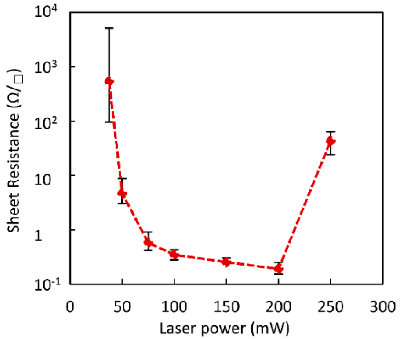
Ultimately, the sintering and melting of the Ag NPs could increase the conduction passes and, therefore, tune the resistance of the Ag membrane. The sheet resistance, which is crucial for RF devices, is plotted in Figure 4. When the Ag membrane was fabricated at a laser power of 37.5 mW, the sheet resistance was at a magnitude around 103 Ω/□. The increase of laser power lead to a rapid drop in sheet resistance by two orders of magnitude, indicating the sintering of the Ag NPs. When the laser power exceeded 75 mW, the decrease of sheet resistance gradually slowed down, with a minimal average value of 0.25 Ω/□ (200 mW). This is consistent with the formation of the continuous silver membrane via sintering and melting (shown in Figure 4c). The corresponding conductivity was 106 S/m (200 mW), which is comparable to the previous studies. The dramatic rise of the sheet resistance at 250 mW was mainly due to the break of the highly conductive path in the silver membrane via laser ablation. The electrons were transported through the porous carbon flacks with a significantly lower conductivity than the silver membrane. Consequently, it is possible to tune the sheet resistance of the silver membrane with a variation of the laser power.
3.2. RF Characteristics of MS lines
RF components, such as antennas, couplers, and filters, can be formed from MS lines, whereas the resistance of the strip conductors becomes a considerable parameter for laser-scribed MS lines. In this regard, the S-parameters, which quantify how RF signals react with MS lines, were monitored using a vector network analyzer. Moreover, three-dimensional electromagnetic simulations were conducted using CST Studio Suit at a frequency range from 1 GHz to 18 GHz. The parameters for the simulations are according to Table 1.
The S21 spectra, which presents the transmission of RF signals through MS lines, is shown in Figure 5. Here, five MS line samples with sheet resistances of 0.25 Ω/□, 0.32 Ω/□, 0.52 Ω/□, 4.61 Ω/□, and 186.3 Ω/□ were chosen for the simulation and test. The corresponding laser powers were 200 mW, 150 mW, 100 mW, 75 mW, 50 mW, and 37.5 mW, respectively. Figure 5a plots the simulation results. The black dash line shows the idea conditions where the sheet resistance is set as zero. The slightly decrease of S21 at a frequency below 7 GHz and the wavy shaped curves at higher frequencies are mainly attributed to the impedance discontinuities between the SMA connectors and the MS line. When sheet resistance is below 0.52 Ω/□, the S21 spectra illustrates a similar variation trend to the idea case. The minute differences between curves are partially due to the ohmic losses from the strip conductors that convert electromagnetic waves to Joule heat [13,14]. Further increasing the sheet resistance to 4.61 Ω/□ tremendously reduced the signals transmitted through the MS lines. The S21 values decreased to around −12 dB, accordingly. Given a more extreme example with a sheet resistance of 183.6 Ω/□, the S21 values dropped well below −20 dB, and even smaller than −40dB at a frequency below 9 GHz. Note that the presence of resistance can result in an impendence mismatch, whereby the reflection will also reduce the transmit signal lead to a drop of S21. The reflection will be discussed with the S11 parameter.
The experimental results plotted in Figure 5b are consistent with the simulation results. Compared with the simulations, faster decreases of the S21 values with an increasing frequency can be attributed to the non-uniformity and discontinuity of the laser-scripted conductors on a micro scale, which increased losses and reflections in higher frequencies. This result also explains the significantly lower S21 at sheet resistances exceeding 0.52 Ω/□. The surface roughness of the samples prepared with a lower laser power is obviously higher than those prepared with a relatively higher laser power.
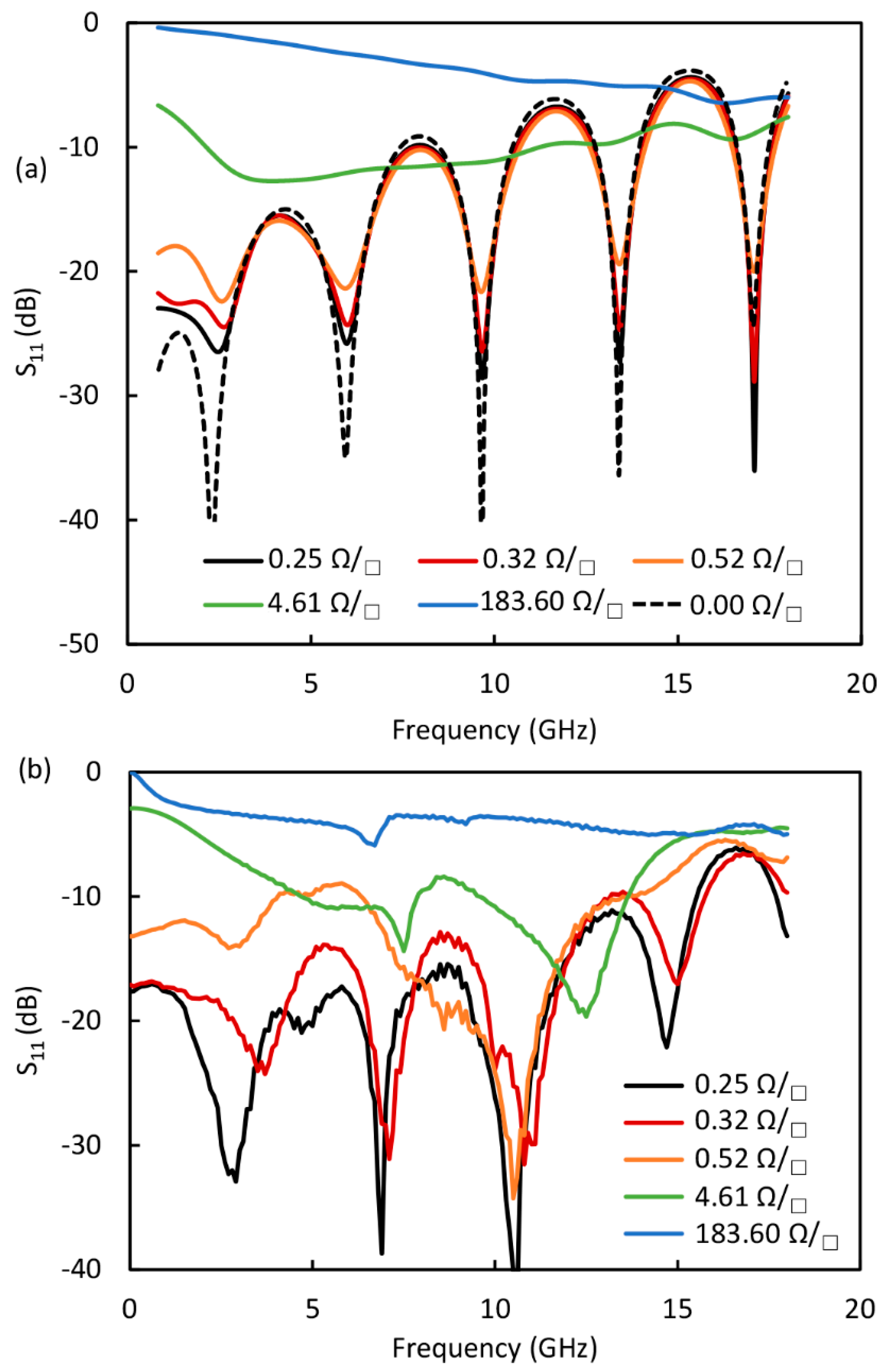
The S11 spectra illustrates the reflection of RF signals (shown in Figure 6). The periodic curves can be attributed to the discontinuities between the MS line and connectors, which are consisted with the S21 spectra in Figure 5. The reflection is approximate to the idea of conduction (sheet resistance is zero), with sheet resistances below 0.52 Ω/□ for simulations and below 0.32 Ω/□ for experiments. On the other hand, the reflection of the signal is more pronounced if we further increase the sheet resistance. S11 values around −10 dB and above −5 dB were observed when the sheet resistances were 4.61 Ω/□ and 183.60 Ω/□, respectively.
For a lossy transmission line with a relatively low resistive loss, such as 0.25 Ω/□ or 0.32 Ω/□, the characteristic impedance Z0 can be written as [13]
where R, G, L, and C are the resistance, conductance, inductance, and capacitance per unit length of the MS line, and ω is the angular frequency of the RF signal. Given a load impendence of ZL, The reflection coefficient Γ0 is written as [13]
From Equation (1) and (2), we can deduce that the presence of sheet resistance leads to a complex characteristic impedance. For our test systems, the ZL is typically set as a standard impendence of 50 Ω. The complex Z0 leads to a nonzero Γ0, which implies the reflection of the RF signal. This reflection will be more significant if we further increase the resistive part for the MS lines. Thus, minimizing the resistance could reduce the reflection of the RF signal for an MS line. Otherwise, complicated matching networks are indispensable to reducing reflection for practical applications. In our case, sheet resistance below 0.32 Ω/□ with a corresponding laser power of 150 mW is preferable for interconnection applications. On the other hand, the transmission and reflections can be tuned via a simple variation of the laser power, which is beneficial to a more flexible design for RF devices. This variation may also simplify the fabrication of resistive components and other functional structures by integrating them into a single step, leading to flexible and low-cost manufacturing.
4. Conclusions
We used a CW laser to in-situ reduce silver ink film on flexible PI substrates for MS transmission lines. The laser-introduced photothermal effects, which can trigger the sintering and melting of laser produced silver nanostructures, could also increase the conduction passes. Therefore, we were able to tune the sheet resistance of the strip conductors via a variation of the laser power. The RF characteristics of laser-scribed MS transmission lines were investigated. The experimental results match well with the simulation data. When the sheet resistance was not above 0.32 Ω/□, the transmission characteristics of the MS lines were insensitive to the sheet resistance and similar to an ideal condition. Moreover, the transmission and reflection characteristics of the MS lines could be simply modified by accommodating the resistance of the strip conductors. LDW provides a simplified method of integrating the fabrication of resistive components and other functional structures into a single step. This simplification promotes flexible and low-cost manufacturing, and may be beneficial for the device’s design.
Author Contributions
R.L., Y.Y., and Y.F. conceived and designed the experiments; R.L. and Y.Y. performed the experiments; R.L., X.Y., and X.F. performed the simulations; L.S. and Y.Y. analyzed the data; and D.D. contributed materials. R.L. and J.Y. wrote the manuscript.
Funding
This research was funded by the National Natural Science Foundation of China (61704090), the Natural Science Foundation of Jiangsu Province (BK20170908, BK20170903), the Natural Science Foundation of the Higher Education Institutions of Jiangsu Province (17KJB510041, 17KJB510040, 17KJA470005), the National and Local Joint Engineering Laboratory of RF Integration and Micro-Assembly Technology (KFJJ20170307, KFJJ20170204, KFJJ20180201), and NUPTSF (NY217123, NY217124).
Conflicts of Interest
The authors declare no conflict of interest.
References
- Zheng, C.; Hu, A.; Kihm, K.D.; Ma, Q.; Li, R.; Chen, T.; Duley, W. Femtosecond Laser Fabrication of Cavity Microball Lens (CMBL) inside a PMMA Substrate for Super-Wide Angle Imaging. Small 2015, 11, 3007–3061. [Google Scholar] [CrossRef] [PubMed]
- Tao, L.Q.; Tian, H.; Liu, Y.; Ju, Z.Y.; Pang, Y.; Chen, Y.Q.; Wang, D.Y.; Tian, X.G.; Yan, J.C.; Deng, N.Q.; et al. An intelligent artificial throat with sound-sensing ability based on laser induced graphene. Nat. Commun. 2017, 8, 14579. [Google Scholar] [CrossRef] [PubMed] [Green Version]
- Hu, A.; Li, R.; Bridges, D.; Zhou, W.; Bai, S.; Ma, D.; Peng, P. Photonic nanomanufacturing of high performance energy devices on flexible substrates. J. Laser Appl. 2016, 28, 022602. [Google Scholar] [CrossRef]
- Yu, Y.; Wang, S.; Ma, D.; Joshi, P.; Hu, A. Recent Progress on Laser Manufacturing of Microsize Energy Devices on Flexible Substrates. JOM 2018, 70, 1816–1822. [Google Scholar] [CrossRef]
- Zhang, Y.; Guo, L.; Wei, S.; He, Y.; Xia, H.; Chen, Q.; Sun, H.-B.; Xiao, F.-S. Direct imprinting of microcircuits on graphene oxides film by femtosecond laser reduction. Nano Today 2010, 5, 15–20. [Google Scholar] [CrossRef]
- Xu, B.B.; Xia, H.; Niu, L.G.; Zhang, Y.L.; Sun, K.; Chen, Q.D.; Xu, Y.; Lv, Z.Q.; Li, Z.H.; Misawa, H. Flexible Nanowiring of Metal on Nonplanar Substrates by Femtosecond-Laser-Induced Electroless Plating. Small 2010, 6, 1762–1766. [Google Scholar] [CrossRef] [PubMed]
- Li, R.-Z.; Peng, R.; Kihm, K.; Bai, S.; Bridges, D.; Tumuluri, U.; Wu, Z.; Zhang, T.; Compagnini, G.; Feng, Z. High-rate in-plane micro-supercapacitors scribed onto photo paper using in situ femtolaser-reduced graphene oxide/Au nanoparticle microelectrodes. Energy Environ. Sci. 2016, 9, 1458–1467. [Google Scholar] [CrossRef]
- In, J.B.; Hsia, B.; Yoo, J.-H.; Hyun, S.; Carraro, C.; Maboudian, R.; Grigoropoulos, C.P. Facile fabrication of flexible all solid-state micro-supercapacitor by direct laser writing of porous carbon in polyimide. Carbon 2015, 83, 144–151. [Google Scholar] [CrossRef]
- El-Kady, M.F.; Strong, V.; Dubin, S.; Kaner, R.B. Laser scribing of high-performance and flexible graphene-based electrochemical capacitors. Science 2012, 335, 1326–1330. [Google Scholar] [CrossRef]
- Gao, W.; Singh, N.; Song, L.; Liu, Z.; Reddy, A.L.; Ci, L.; Vajtai, R.; Zhang, Q.; Wei, B.; Ajayan, P.M. Direct laser writing of micro-supercapacitors on hydrated graphite oxide films. Nat. Nanotechnol. 2011, 6, 496–500. [Google Scholar] [CrossRef]
- Cheng, C.; Wang, S.; Wu, J.; Yu, Y.; Li, R.; Eda, S.; Chen, J.; Feng, G.; Lawrie, B.; Hu, A. Bisphenol A Sensors on Polyimide Fabricated by Laser Direct Writing for Onsite River Water Monitoring at Attomolar Concentration. ACS Appl. Mater. Interfaces 2016, 8, 17784–17792. [Google Scholar] [CrossRef] [PubMed]
- Griffiths, K.; Dale, C.; Hedley, J.; Kowal, M.D.; Kaner, R.B.; Keegan, N. Laser-scribed graphene presents an opportunity to print a new generation of disposable electrochemical sensors. Nanoscale 2014, 6, 13613–13622. [Google Scholar] [CrossRef] [PubMed] [Green Version]
- Antti, V.; Lehto, A. Radio Engineering for Wireless Communication and Sensor Applications; Artech House: Boston, MA, USA, 2003. [Google Scholar]
- Hong, J.-S.G.; Lancaster, M.J. Microstrip Filters for RF/Microwave Applications; John Wiley & Sons: New York, NY, USA, 2004; Volume 167. [Google Scholar]
- Bahl, I.; Stuchly, S.S. Analysis of a microstrip covered with a lossy dielectric. IEEE Trans. Microw. Theory Tech. 1980, 28, 104–109. [Google Scholar] [CrossRef]
- Lederer, D.; Raskin, J.-P. Substrate loss mechanisms for microstrip and CPW transmission lines on lossy silicon wafers. Solid State Electron. 2003, 47, 1927–1936. [Google Scholar] [CrossRef]
- Ponchak, G.E.; Downey, A.N. Characterization of thin film microstrip lines on polyimide. IEEE Trans. Compon. Packag. Manuf. Technol. Part B 1998, 21, 171–176. [Google Scholar] [CrossRef]
- Zhou, W.; Bai, S.; Ma, Y.; Ma, D.; Hou, T.; Shi, X.; Hu, A. Laser-direct writing of silver metal electrodes on transparent flexible substrates with high-bonding strength. ACS Appl. Mater. Interfaces 2016, 8, 24887–24892. [Google Scholar] [CrossRef] [PubMed]
- Song, Y.-J.; Wang, M.; Zhang, X.-Y.; Wu, J.-Y.; Zhang, T. Investigation on the role of the molecular weight of polyvinyl pyrrolidone in the shape control of high-yield silver nanospheres and nanowires. Nanoscale Res. Lett. 2014, 9, 1–8. [Google Scholar] [CrossRef] [PubMed]
- Li, R.Z.; Hu, A.; Bridges, D.; Zhang, T.; Oakes, K.D.; Peng, R.; Tumuluri, U.; Wu, Z.; Feng, Z. Robust Ag nanoplate ink for flexible electronics packaging. Nanoscale 2015, 7, 7368–7377. [Google Scholar] [CrossRef] [PubMed]
- Zhu, S.-Q.; Zhang, T.; Guo, X.-L.; Zhang, X.-Y. Self-assembly of large-scale gold nanoparticle arrays and their application in SERS. Nanoscale Res. Lett. 2014, 9, 1–9. [Google Scholar] [CrossRef]
- Li, R.-Z.; Hu, A.; Zhang, T.; Oakes, K.D. Direct writing on paper of foldable capacitive touch pads with silver nanowire inks. ACS Appl. Mater. Interfaces 2014, 6, 21721–21729. [Google Scholar] [CrossRef] [PubMed]
- Zhang, X.-Y.; Shan, F.; Zhou, H.-L.; Su, D.; Xue, X.-M.; Wu, J.-Y.; Chen, Y.-Z.; Zhao, N.; Zhang, T. Silver nanoplate aggregation based multifunctional black metal absorbers for localization, photothermic harnessing enhancement and omnidirectional light antireflection. J. Mater. Chem. C 2018, 6, 989–999. [Google Scholar] [CrossRef]
- Peng, P.; Hu, A.; Gerlich, A.P.; Zou, G.; Liu, L.; Zhou, Y.N. Joining of silver nanomaterials at low temperatures: Processes, properties, and applications. CS Appl. Mater. Interfaces 2015, 7, 12597–12618. [Google Scholar] [CrossRef] [PubMed]
Figure 1.
The structure of the laser-scribed MS line. w, l, and ts are the width of the strip conductor, the length of the strip conductor, and the thickness of the polyimide substrate, respectively.
Figure 1.
The structure of the laser-scribed MS line. w, l, and ts are the width of the strip conductor, the length of the strip conductor, and the thickness of the polyimide substrate, respectively.
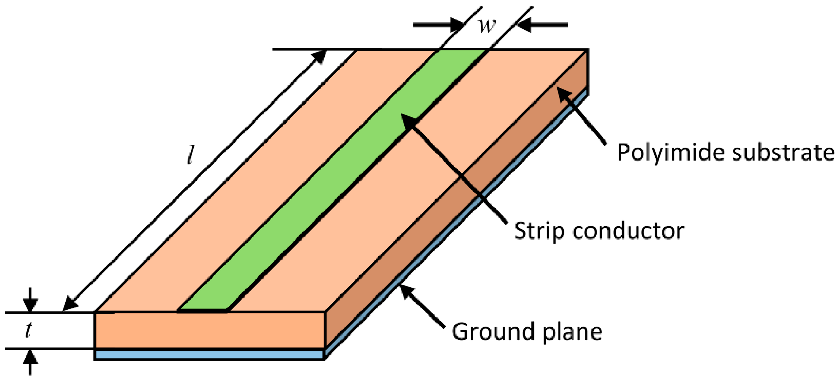
Figure 2.
The laser-scripted MS transmission line on a PI film. (a) The photo image of a MS line. (b) The microscope image of a silver membrane. The inset shows the cross-sectional view of the silver membrane. The scale bar in the inset indicates 10 μm.
Figure 2.
The laser-scripted MS transmission line on a PI film. (a) The photo image of a MS line. (b) The microscope image of a silver membrane. The inset shows the cross-sectional view of the silver membrane. The scale bar in the inset indicates 10 μm.

Figure 3.
Scanning electron microscope images of laser-scripted silver membrane with different laser powers ((a) and (b): 50 mW, (c) and (d): 100 mW, (e) and (f): 150 mW, (g) and (h): 250 mW).
Figure 3.
Scanning electron microscope images of laser-scripted silver membrane with different laser powers ((a) and (b): 50 mW, (c) and (d): 100 mW, (e) and (f): 150 mW, (g) and (h): 250 mW).

Figure 4.
The sheet resistance as a function of laser power.

Figure 5.
S21 spectra at various sheet resistances: (a) simulation results; (b) experiment results.

Figure 6.
S11 spectra at various sheet resistances: (a) simulation results; (b) experiment results.


Table 1.
The parameters of the 50 Ω MS line.
| Parameters | Value |
|---|---|
| Width of the Strip conductor, w | 0.45 mm |
| Length of the Strip conductor, l | 30 mm |
| Thickness of the Strip conductor | 4 μm |
| Thickness of the PI substrate, ts | 0.2 mm |
| Dielectric constant of the PI substrate | 3.5 |
| Loss Tangent of the PI substrate | 0.0027 |
© 2019 by the authors. Licensee MDPI, Basel, Switzerland. This article is an open access article distributed under the terms and conditions of the Creative Commons Attribution (CC BY) license (http://creativecommons.org/licenses/by/4.0/).
Share and Cite
MDPI and ACS Style
Li, R.; Yan, J.; Fang, Y.; Fan, X.; Sheng, L.; Ding, D.; Yin, X.; Yu, Y. Laser-Scribed Lossy Microstrip Lines for Radio Frequency Applications. Appl. Sci. 2019, 9, 415. https://doi.org/10.3390/app9030415
AMA Style
Li R, Yan J, Fang Y, Fan X, Sheng L, Ding D, Yin X, Yu Y. Laser-Scribed Lossy Microstrip Lines for Radio Frequency Applications. Applied Sciences. 2019; 9(3):415. https://doi.org/10.3390/app9030415
Chicago/Turabian StyleLi, Ruozhou, Jing Yan, Yuming Fang, Xingye Fan, Linkun Sheng, Daye Ding, Xiaoxing Yin, and Ying Yu. 2019. "Laser-Scribed Lossy Microstrip Lines for Radio Frequency Applications" Applied Sciences 9, no. 3: 415. https://doi.org/10.3390/app9030415
Note that from the first issue of 2016, this journal uses article numbers instead of page numbers. See further details here.