Deep Electrical Modulation of Terahertz Wave Based on Hybrid Metamaterial-Dielectric-Graphene Structure

Abstract
:1. Introduction
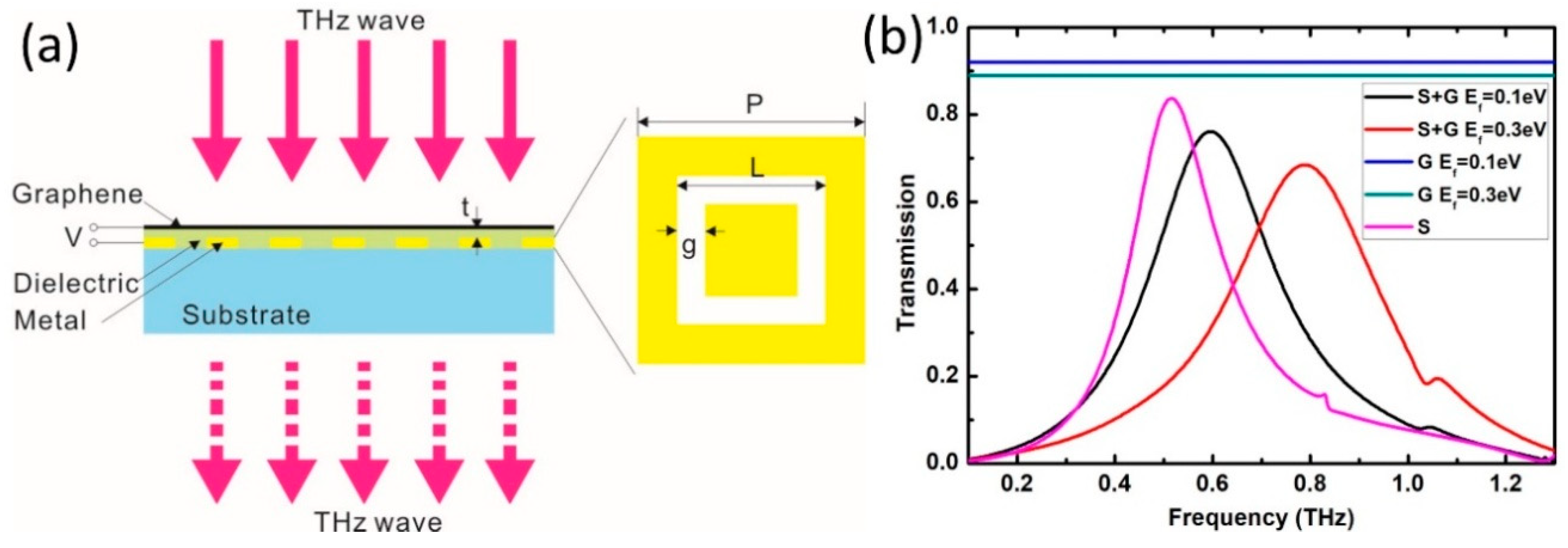
2. Device Structure
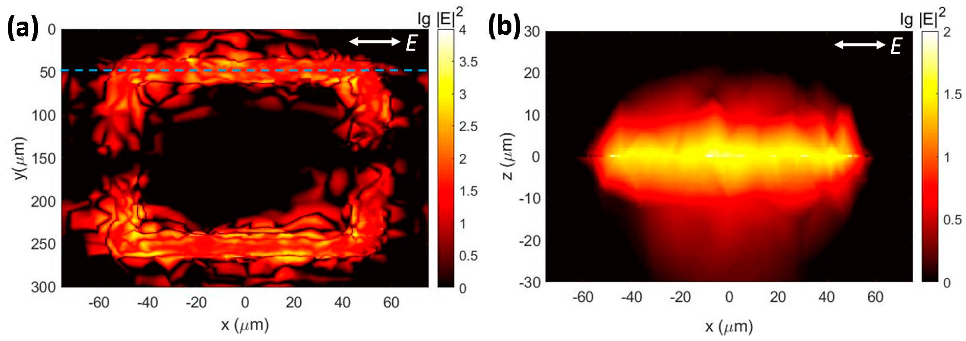
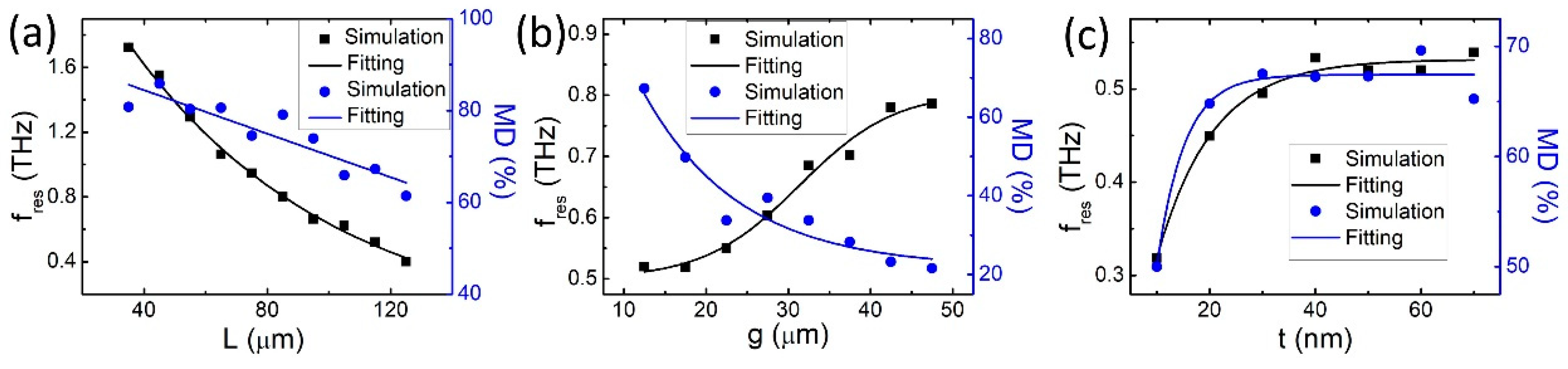
3. Simulations
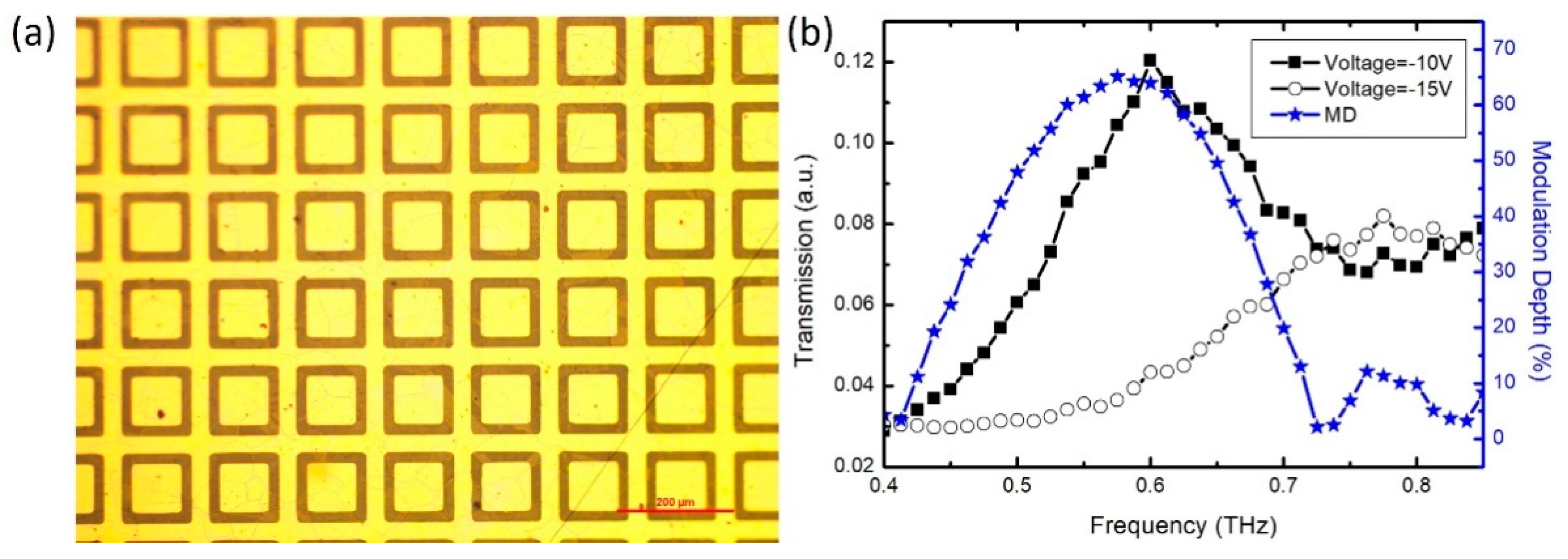
4. Measurements
5. Conclusions
Author Contributions
Funding
Conflicts of Interest
References
- Federici, J.F.; Schulkin, B.; Huang, F.; Gary, D.; Barat, R.; Oliveira, F.; Zimdars, D. THz imaging and sensing for security applications: Explosives, weapons and drugs. Semicond. Sci. Tech. 2005, 20, S266. [Google Scholar] [CrossRef]
- Krumbholz, N.; Gerlach, K.; Rutz, F.; Koch, M.; Piesiewicz, R.; Kürner, T.; Mittleman, D. Omnidirectional terahertz mirrors: A key element for future terahertz communication systems. Appl. Phys. Lett. 2006, 88, 202905. [Google Scholar] [CrossRef]
- Fitzgerald, A.J.; Berry, E.; Zinovev, N.N.; Walker, G.C.; Smith, M.A.; Chamberlain, J.M. An introduction to medical imaging with coherent terahertz frequency radiation. Phys. Med. Biol. 2002, 47, R67. [Google Scholar] [CrossRef] [PubMed]
- Foschini, G.J.; Golden, G.D.; Valenzuela, R.A.; Wolniansky, P.W. Simplified processing for high spectral efficiency wireless communication employing multi-element arrays. IEEE J. Sel. Area. Commun. 1999, 17, 1841–1852. [Google Scholar] [CrossRef] [Green Version]
- Mesleh, R.; Elgala, H.; Haas, H. On the performance of different OFDM based optical wireless communication systems. J. Opt. Commun. Netw. 2011, 3, 620–628. [Google Scholar] [CrossRef]
- Cho, K.; Yoon, D. On the general BER expression of one-and two-dimensional amplitude modulations. IEEE Trans. Commun. 2002, 50, 1074–1080. [Google Scholar]
- Kleine-Ostmann, T.; Pierz, K.; Hein, G.; Dawson, P.; Koch, M. Audio signal transmission over THz communication channel using semiconductor modulator. Electron. Lett. 2004, 40, 124–126. [Google Scholar] [CrossRef]
- Sabah, C. Tunable metamaterial design composed of triangular split ring resonator and wire strip for S-and C-microwave bands. Prog. Electromagn. Res. 2010, 22, 341–357. [Google Scholar] [CrossRef]
- Holl, P.; Kemmer, J.; Prechtel, U.; Ziemann, T.; Hauff, D.; Lutz, G.; Schwarz, A. A double-sided silicon strip detector with capacitive readout and a new method of integrated bias coupling. IEEE Trans. Nuc. Sci. 1989, 36, 251–255. [Google Scholar] [CrossRef]
- Bolotin, K.I.; Sikes, K.J.; Jiang, Z.; Klima, M.; Fudenberg, G.; Hone, J.; Kim, P.; Stormer, H.L. Ultrahigh electron mobility in suspended graphene. Solid State Commun. 2008, 146, 351–355. [Google Scholar] [CrossRef] [Green Version]
- Zhu, Y.; Murali, S.; Cai, W.; Li, X.; Suk, J.W.; Potts, J.R.; Ruoff, R.S. Graphene and graphene oxide: Synthesis, properties, and applications. Adv. Mater. 2010, 22, 3906–3924. [Google Scholar] [CrossRef] [PubMed]
- Schwierz, F. Graphene transistors. Nat. Nanotechnol. 2010, 5, 487. [Google Scholar] [CrossRef] [PubMed]
- Tan, W.D.; Su, C.Y.; Knize, R.J.; Xie, G.Q.; Li, L.J.; Tang, D.Y. Mode locking of ceramic Nd: Yttrium aluminum garnet with graphene as a saturable absorber. Appl. Phys. Lett. 2010, 96, 031106. [Google Scholar] [CrossRef]
- Mueller, T.; Xia, F.; Avouris, P. Graphene photodetectors for high-speed optical communications. Nat.Photonics 2010, 4, 297. [Google Scholar] [CrossRef]
- Hill, E.W.; Vijayaragahvan, A.; Novoselov, K. Graphene sensors. IEEE Sens. J. 2011, 11, 3161–3170. [Google Scholar] [CrossRef]
- Sensale-Rodriguez, B.; Yan, R.; Kelly, M.M.; Fang, T.; Tahy, K.; Hwang, W.S.; Jena, D.; Liu, L.; Xing, H.G. Broadband graphene terahertz modulators enabled by intraband transitions. Nat. Commun. 2012, 3, 780. [Google Scholar] [CrossRef] [Green Version]
- Wang, S.; Xia, L.; Mao, H.; Jiang, X.; Yan, S.; Wang, H.; Wei, D.; Cui, H.L.; Du, C. Terahertz biosensing based on a polarization-insensitive metamaterial. IEEE Photonic. Tech. Lett. 2016, 28, 986–989. [Google Scholar] [CrossRef]
- Lu, D.; Liu, Z. Hyperlenses and metalenses for far-field super-resolution imaging. Nat. Commun. 2012, 3, 1205. [Google Scholar] [CrossRef] [Green Version]
- Yuan, G.; Dong, X.; Deng, Q.; Liu, C.; Lu, Y.; Shi, H.; Du, C. A broadband slab lens antenna formed from gradient refractive index metamaterials composed of cross-shaped cells. Microw. Opt. Techn. Lett. 2014, 56, 1124–1129. [Google Scholar] [CrossRef]
- Xu, W.; Xie, L.; Zhu, J.; Tang, L.; Singh, R.; Wang, C.; Ma, Y.; Chen, H.T.; Ying, Y. Terahertz biosensing with a graphene-metamaterial heterostructure platform. Carbon 2019, 141, 618–625. [Google Scholar] [CrossRef]
- He, X.; Lin, F.; Liu, F.; Shi, W. Tunable high Q-factor terahertz complementary graphene metamaterial. Nanotechnology 2018, 29, 485205. [Google Scholar] [CrossRef] [PubMed]
- Xia, L.; Zhang, X.; Wei, D.; Cui, H.L.; Du, C. Graphene terahertz amplitude modulation enhanced by square ring resonant structure. IEEE Photonics J. 2018, 10, 1–7. [Google Scholar] [CrossRef]
- Gao, W.; Shu, J.; Reichel, K.; Nickel, D.V.; He, X.; Shi, G.; Vajtai, R.; Ajayan, P.M.; Kono, J.; Mittleman, D.M.; et al. High-contrast terahertz wave modulation by gated graphene enhanced by extraordinary transmission through ring apertures. Nano Lett. 2014, 14, 1242–1248. [Google Scholar] [CrossRef] [PubMed]
- Ju, L.; Geng, B.; Horng, J.; Girit, C.; Martin, M.; Hao, Z.; Bechtel, H.A.; Liang, X.; Zettl, A.; Shen, Y.R.; et al. Graphene plasmonics for tunable terahertz metamaterials. Nat. Nanotechnol. 2011, 6, 630. [Google Scholar] [CrossRef] [PubMed]
- Sun, F.; Xia, L.; Nie, C.; Shen, J.; Zou, Y.; Cheng, G.; Wu, H.; Zhang, Y.; Wei, D.; Yin, S.; et al. The all-optical modulator in dielectric-loaded waveguide with graphene-silicon heterojunction structure. Nanotechnology 2018, 29, 135201. [Google Scholar] [CrossRef] [PubMed] [Green Version]
- Mao, Q.; Wen, Q.Y.; Tian, W.; Wen, T.L.; Chen, Z.; Yang, Q.H.; Zhang, H.W. High-speed and broadband terahertz wave modulators based on large-area graphene field-effect transistors. Opt. Lett. 2014, 39, 5649–5652. [Google Scholar] [CrossRef] [PubMed]


| Graphene Based THz Amplitude Modulation | Amplitude Modulation Depth |
|---|---|
| Graphene/SiO2/pSi [16] | 15% |
| Graphene/Al2O3/pSi [26] | 22% |
| Metallic circle ring/Graphene/SiO2/pSi [23] | 50% |
| Metallic square ring/PMMA/Graphene/PET (this work) | 65.1% |
© 2019 by the authors. Licensee MDPI, Basel, Switzerland. This article is an open access article distributed under the terms and conditions of the Creative Commons Attribution (CC BY) license (http://creativecommons.org/licenses/by/4.0/).
Share and Cite
Xia, L.; Zhang, X.; Zhang, M.; Dang, S.; Huang, S.; Tan, Y.; Yan, W.; Cui, H.-L. Deep Electrical Modulation of Terahertz Wave Based on Hybrid Metamaterial-Dielectric-Graphene Structure. Appl. Sci. 2019, 9, 507. https://doi.org/10.3390/app9030507
Xia L, Zhang X, Zhang M, Dang S, Huang S, Tan Y, Yan W, Cui H-L. Deep Electrical Modulation of Terahertz Wave Based on Hybrid Metamaterial-Dielectric-Graphene Structure. Applied Sciences. 2019; 9(3):507. https://doi.org/10.3390/app9030507
Chicago/Turabian StyleXia, Liangping, Xin Zhang, Man Zhang, Suihu Dang, Shijian Huang, Yong Tan, Wenjuan Yan, and Hong-Liang Cui. 2019. "Deep Electrical Modulation of Terahertz Wave Based on Hybrid Metamaterial-Dielectric-Graphene Structure" Applied Sciences 9, no. 3: 507. https://doi.org/10.3390/app9030507