Review

Review of the CdCl2 Treatment Used in CdS/CdTe Thin Film Solar Cell Development and New Evidence towards Improved Understanding

Electronic Materials and Sensors Group, Materials and Engineering Research Institute, Sheffield Hallam University, Sheffield S1 1WB, UK
Coatings 2014, 4(2), 282-307; https://doi.org/10.3390/coatings4020282
Submission received: 18 February 2014 / Revised: 17 April 2014 / Accepted: 24 April 2014 / Published: 30 April 2014
(This article belongs to the Special Issue Novel Thin Film Materials for Photovoltaic Applications)

Abstract

:
Cadmium chloride treatment is a key processing step identified in the late 1970s to drastically improve the solar to electric conversion efficiency of CdS/CdTe thin film solar cells. Although a large body of experimental results are available to date, this process is yet to be understood even after three decades of research. This paper reviews the experimental results available, presents some new clues leading to improved understanding and suggests key research areas necessary to fully understand this crucial processing step. Improved understanding will lead to further increase in conversion efficiency of CdS/CdTe solar cells well beyond 20%.

1. Introduction

Cadmium telluride (CdTe)-based thin film solar cells have attracted worldwide research attention over the past three decades, in order to develop low-cost and high efficiency solar panels suitable for photovoltaic (PV) solar energy conversion. This work has resulted in ~17.0%–20.4% lab-scale efficiency [1,2,3,4,5] with 16.1% module efficiency [6], and First Solar Company in the US, is currently leading the PV manufacturing of thin film CdTe solar panels. In CdTe solar cell research and development programme, “CdCl2 treatment” is a key step for a drastic improvement of the solar to electric conversion efficiency. This treatment has been known to the scientific community since 1976 [7] and subsequently, this processing step has been used by numerous research groups by modifying its method of application. The treatment consists of growth or post-growth heat treatment of CdTe layers in the presence of CdCl2 or halogens (mostly, chlorine, and fluorine) molecules, atoms or ions. Post-growth heat treatment is usually carried out at temperatures in the range 350–450 °C for 60–20 min duration under atmospheric conditions. This treatment drastically enhances the solar cell efficiency from about 1%–5% for as-grown materials to double-digit figures for CdCl2-treated materials. This is almost an order of magnitude increase in conversion efficiency. Although a huge research effort has been made to understand the science behind this processing step, this goal has not yet been fully achieved. For this reason, some of the scientific publications in the literature label this crucial step as an “empirical magic production step” [8]. This article attempts to contribute towards the understanding of this processing step by reviewing the published work and combining it with emerging new observations. Proper understanding will lead to breaking the stagnation in efficiency improvement over the past two decades, help in enhancing the current efficiencies further, as well as help in reducing the $W−1 figure for CdTe-based thin film solar panels.
Section 2 and Section 3 of this paper review the results already reported in the literature and present new emerging experimental evidence on this processing step. Section 4 critically discusses and analyses the wealth of knowledge already available on this processing step. Finally, Section 5 suggests further key experiments most relevant to probing and unravelling the secrets behind this processing step.

2. Summary of Reported Results

The CdCl2 treatment is usually applied for thin film CdTe layers grown by any large area deposition method (vacuum evaporation, sputtering, close space sublimation, electrodeposition, and screen printing) before fabricating photovoltaic (PV) solar cells. CdTe-based thin film solar cell has the basic structure of glass/TCO/CdS/CdTe/electrical contact, with CdS and CdTe as the two basic semiconducting layers. Some groups have reported 10–50 nm as the optimum CdS thickness for the best devices [9] while others have used CdS layers with thickness up to 1–2 µm [10,11]. The thickness of CdTe layer varies from 1.5 µm to ~8.0 µm [11,12]. The transparent conducting oxides (TCO) frequently used are indium tin oxide (ITO) and fluorine-doped tin oxide (FTO). Thickness of the TCO layers vary in the range of 200–400 nm with high transparency and low sheet resistance in the range 7–15 Ω/□. The usual practice of CdCl2 treatment is to spread a saturated solution or suspension of CdCl2 in water or methanol on CdTe surface, allow the solvent to evaporate and then heat-treat the structure at high temperatures up to 450 °C for a selected period of time in air atmosphere. White CdCl2 powder is clearly visible on the dark surface of CdTe after this process. Some groups have alternatively deposited a layer of CdCl2 by methods such as vacuum evaporation and laser ablation for the treatment of both CdS and CdTe layers [12,13,14,15,16,17,18]. In the case of electrodeposition, addition of CdCl2 into the electrolytic bath is another method of CdCl2 treatment [19]. Recently, researchers started to use Freon gas (HCClF2) for post-growth annealing treatment of CdTe thin films produced by vacuum evaporation methods, such as closed space sublimation (CSS) [20]. In this method, halogen (Cl and F) molecules, atoms, or ions are present at the CdTe/gas interface during the heat treatment of CdTe layer at high temperatures (up to ~650 °C). This method produces solar cells with efficiencies ~16% and allows scaling up with consistent results. The following sections briefly summarise various conclusions made by different research groups on this CdCl2 treatment and Section 4 critically discusses the consequences of these observations on device performance.

2.1. Recrystallisation and Grain Growth

The most common analytical methods used to study both as-grown and CdCl2-treated CdTe layers for comparison are X-ray diffraction (XRD), scanning electron microscopy (SEM), and atomic force microscopy (AFM). Numerous reports [21,22,23,24,25,26] conclude that the XRD peaks observed show recrystallisation and grain growth after CdCl2 treatment. Heat treatment alone, without CdCl2, also shows this trend, but the presence of CdCl2 enhances the recrystallisation. This observation is widely accepted for CdTe layers consisting of small grains before post-deposition heat treatment. SEM and AFM work on both as-grown and CdCl2-treated CdTe layers also complement this conclusion [21,22,23,24,25].
Many research articles have reported the existence of (111) preferred orientation for low temperature-grown CdTe layers and the increase in peak intensity with CdCl2 treatment. However, some research groups have reported that as-grown CdTe layers have (111) preferred orientation but after CdCl2 treatment, the intensity of the (111) peak reduces and the other two peaks (220) and (311) become visible and the material therefore loses the preferential orientation along the (111) plane and becomes poly-crystalline [20,21,22,23,24,25,26,27]. There are also reports concluding that there is no grain growth if the starting CdTe layer has large grains [9]. These layers are typically grown by high-temperature CSS method and the grains lock-up in their structure without showing any further grain growth. However, during CdCl2-treatment, smaller grains disappear and regenerated grains are observed [18]. In both cases, whether there is grain growth or not, the CdCl2 treatment leads to a considerable enhancement of device efficiency.
Recent research reported in 2011 by Kim et al. [28] shows that this group has carried out comprehensive work to clarify this recrystallisation during CdCl2 treatment. They have carried out a large number of time-resolved high temperature X-ray diffraction in situ as a function of both temperature, and duration of annealing at a constant temperature to record and map the peaks for a thorough investigation. These results clearly show that the material layers crystallise between 300 °C and 385 °C, in the (111) preferred orientation. However, heat treatment after 385 °C drastically reduces the (111) peak intensity and the other two peaks (220) and (311) grow in intensity rapidly. The authors confirmed that after ~385 °C, the crystal structure transforms into random orientations showing re-organisation of the grains. This work also concluded that the rearrangement of grains is due to Cl diffusion into CdTe.
This particular report [28] explains and clarifies the differing reports present in the literature on the CdTe grains orientation. If the growth temperature or annealing temperature is below the transition at ~385 °C, (111) preferred orientation is dominant, but the intensity of (111) collapses and the intensities of (220) and (311) peaks increase showing the re-orientation of grains if the annealing temperature passes this transition temperature of ~385 °C. As discussed in Section 2.1, the materials grown or heat-treated at temperatures below 385 °C show a strong preferential orientation along (111) direction with only very small detectable two peaks from (220) and (311) planes. When grown or heat-treated at temperatures above 385 °C, the layers show all three peaks in their XRD patterns with comparable intensities. It is highly relevant to explore whether the (111) oriented CdTe or the randomly oriented CdTe films produce the highest efficiency values. These structure and device property relationships are essential to research in the future.

2.2. Interactions at CdS/CdTe Interface

There are also reports [10,13,17,24] published using analytical techniques, such as X-ray photoelectron spectroscopy (XPS), Raman spectroscopy, photoluminescence (PL), cathodoluminescense (CL), etc., in order to investigate the changes happening at the CdS/CdTe hetero-junction during CdCl2 treatment. These studies conclude that the CdCl2 treatment enhances the in- and out-diffusion of semiconductor constituent atoms (S and Te) and, therefore, intermixing at the interface. The production of a ternary compound (CdSxTe1−x), and creation of a graded bandgap structure instead of an abrupt-interface is beneficial in device performance. Removal of lattice mismatch, stress, and surface states are the main advantages of this interface reaction that lead to the improvement of device performance.
It should also be noted that there is a publication reporting that CdCl2 treatment does not significantly affect the intermixing at the CdS/CdTe interface even at treatment temperatures up to 460 °C [14]. These researchers however suggest that the electronic properties of the layers are affected and improved during CdCl2 treatment.

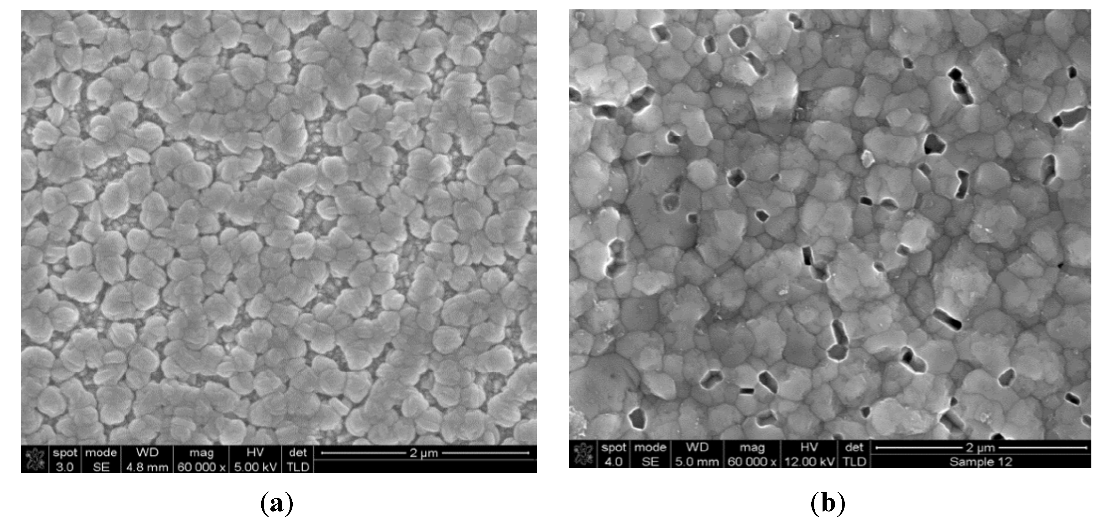
2.3. Increase in Surface Roughness

Some research groups have also used the 2D-AFM technique for comparing surface roughness of the CdTe surfaces before and after CdCl2 treatment [19,22,23]. Results reported show that the surface roughness increases after CdCl2 treatment. These observations agree well with recrystallisation and grain growth as described in Section 2.1. Reported results also indicate that CdTe grows as columns in thin films [29] and this nature, together with recrystallisation, produces large grains comparable to the thickness of CdTe layers. As a result of the columnar growth and recrystallisation, the surface roughness of thin films increases with CdCl2 treatment. This surface roughness could create discontinuities in the back metal contact if the contacting metal layer thickness is less than the surface roughness of CdTe surface. This disadvantage can be removed by using thicker back electrical contacts in device fabrication.

2.4. Enhancement of Lifetime of Charge Carriers

Thoughtful experiments such as PL have been carried out in order to explore changes in lifetime of charge carriers in CdTe before and after CdCl2 treatment [13,22]. For high efficiency solar cells, long lifetime of photo-generated charge carriers are desirable in order to separate and transfer charge carriers towards electrical contacts before their recombination. Reported results indeed show that increase of lifetime of charge carriers in CdTe depends on post-growth annealing steps. Metzger et al. [13] reported the carrier lifetime of 50–300 ps for as-grown CdTe layers, and 700–1000 ps for CdTe grown on FTO/CdS and treated with CdCl2. This work clearly shows the benefits of the presence of CdS and CdCl2 treatment, and 700–1000 ps is the typical lifetime range of charge carriers in CdTe material used for high efficiency devices. Experimental results in this area are scarce and therefore these measurements are useful in understanding the effect of CdCl2 treatment in CdS/CdTe solar cell development.

2.5. Change of Electrical Conductivity and Doping Concentration

Investigation of changes in electrical conductivity of CdTe before and after CdCl2 treatment is a crucial step towards understanding this processing step. Several groups have reported these results but there are no consistent conclusions [30,31]. Some groups reported increase of electrical conduction [30,31], but the most important parameter, which is the electrical conduction after CdCl2 treatment, has not been systematically studied and reported. A Group VII element, Cl, is a well-known n-type dopant in CdTe when Cl dopants replace Te atoms in ppm levels [32,33]. However, Cl also seems to be a p-type dopant when Cl makes complexes with currently un-known native defects in CdTe. This needs careful investigation in order to understand the CdCl2 treatment. In addition to the above complication, there is another basic drawback in these research activities. CdTe is a material that can exist in p-type, i-type or n-type conduction modes depending on the material composition and external dopants added [31,32,33]. Te-rich CdTe layers act as p-type and Cd-rich CdTe layers act as n-type materials (see Section 3.1). Unfortunately, many research carried out in the past have ignored to experimentally find out the electrical conduction type of the starting CdTe layer. Most of the discussions of experimental results were based on an assumed p-type electrical conduction of the starting CdTe layer, and this assumption is the main reason for this confusion. Addition of an n-type dopant (Cl) to CdTe could show different results depending on the initial electrical conduction type of the starting material. The electrical conduction increases if the starting material is n-type and decreases due to self-compensation if the starting material is p-type, when Cl behaves as a shallow donor. When chlorine makes complexes with native defects, acting as a p-dopant, the situation becomes more complex. This area is therefore extremely important, and invokes systematic and comprehensive research, in order to understand the effect of CdCl2 treatment on CdTe thin films.

2.6. Passivation of Grain Boundaries

CdTe thin films are poly-crystalline and the grain size depends on the growth method, substrate used and growth temperature during deposition. For example, most common high temperature techniques, such as CSS, produce large grains, and low-temperature methods, such as electroplating, sputtering, and vacuum evaporation, produce comparatively small grains. In all cases, CdTe is known to show columnar growth leaving large amounts of grain boundaries in the layer [29]. Most recent 3D-AFM results [25,34,35] show that both CdS and CdTe layers grown by electroplating exhibit tightly packed, rod-type grains. In this situation, a large number of grain boundaries perpendicular to the substrate exist in large densities, and Cl and O diffusion along these easy diffusion paths could take place during CdCl2 treatment in air. Therefore, the surface passivation and doping effects at grain boundaries are extremely important to explore and understand. The techniques, such as electron beam induced current (EBIC), are of paramount importance in this research to investigate the current collection patterns during PV process.
It is important to note that the application of CdCl2 on CdTe layer and subsequent heat treatment should be carried out in the presence of oxygen in order to achieve highest efficiencies [15]. This can be achieved by using normal atmospheric conditions, exposing to O2 ambient, or in the case of CdTe growth in a vacuum chamber, inserting halogen containing gas, such as Freon and O2 gas mixture, to the chamber during the growth. Removal of O2 environment leads to formation of comparatively poor devices. Therefore, the inclusion of oxygen in the device structure has a very important role together with CdCl2 treatment [36]. In order to simplify the CdCl2 treatment, researchers have used vapours of CdCl2 or HCl during growth of CdTe in the CSS process. However, although Cl was present, the devices produced in the absence of oxygen show poor performance mainly due to low FF values [36]. It seems therefore, that there are two helpful effects arising from oxygen and halogens (Cl and F), which lead to the improvement of CdS/CdTe solar cells. These effects need to be fully explored and identified through careful experimentation in order to improve our understanding.
A report of comprehensive CL studies [14] on CSS-CdTe layers show that after CdCl2 treatment, small grains and the periphery of large grains are dominated by p-type doping, whereas the centres of large grains are dominated by n-type doping. This is an interesting experimental observation. However, in the same report, the assumption of CSS-CdTe as p-type material contradicts the n-type nature of the centres of large grains. This highlights the necessity of experimentally finding the electrical conduction type of CdTe layers, instead of assuming, in order to draw definite and accurate conclusions.

2.7. Defects in CdS and CdTe Layers

The defects present in the two material layers (CdS and CdTe) and at their interfaces are of paramount importance in determining the final device performance. These defects can act as recombination centres during PV process and reduce device parameters drastically. The interface states could pin the Fermi level, and fix the potential barrier present, thereby strongly affecting the open circuit voltage and other parameters in thin film solar cells [2,37]. In order to determine the defects in CdCl2-treated and untreated device structures, the techniques like PL [13,17], DLTS [15], CL [14,20], and photo-capacitance [24] have been carried out. The CL studies show that there is a formation of defect level just above the valence band (see Figure 2 in Section 3.2), converting the material towards p-type electrical conduction [20]. The use of different techniques shows the presence of numerous defects in CdTe [33,37,38,39] and the device structure, but it is difficult to confirm which defect is dominant in controlling the electrical properties of the completed device. Electrical contact work, such as Schottky barrier height measurements using the I-V technique [2], are more relevant, and should be used to determine the electrically dominant defect levels in these solar cell device structures.
In addition to these intrinsic or native defects within the materials, extrinsic defects, such as pinholes, are also important in device fabrication. These are discussed in the next section under interface morphology.

2.8. Interface Morphology

The thickness of the thinnest CdS/CdTe solar cell is ~1.5 µm and therefore the surface and interface morphologies play very important roles. A clear understanding of the growth modes of CdS and CdTe layers is essential in this device development programme. Electronic material layers usually grow in three different modes; layer-by-layer growth mode, layer and cluster growth (Stransky-Krastanov growth) mode and cluster formation growth mode. For thin film development programmes, the most desired growth mode is the layer-by-layer growth mechanism. Otherwise the expected PV active planar junctions are not formed and the devices will be short-circuited via pinholes and gaps in-between the material grains. The use of TCOs with surface roughness comparable to the thickness of CdS (~100 nm) complicates the matter further.
Most of the analytical techniques used in the past to study the morphology of CdS and CdTe layers are two-dimensional SEM and AFM. These techniques allow us to observe the top surfaces, and SEM cross-section studies also provide information on the nature of grain growth, with some limitations. Over the past two to three decades, 80–100 nm-thick CdS layers prepared by chemical bath deposition (CBD-CdS) have been used and identified as collection of nanoparticles with diameters varying from ~10 to 50 nm [9].
A few microns-thick CdTe layers have been identified as micron-size large grains showing columnar-type growth pattern [29]. These grain sizes vary depending on the growth technique used, as expected, from 14 different possible growth methods identified for CdTe [9]. Although the growth techniques are very different, the most striking feature is that the CdTe materials grown by all these different methods produce over 10% efficiency only after CdCl2 treatment.
The most commonly used CdS layer is normally grown by CBD method, but different growth techniques have been used for CdTe growth and the grain sizes are very different. Therefore, the surface and interface morphologies must be different for as-grown CdTe materials, with numerous leakage paths. The CdCl2 treatment in the presence of O2 seems to drastically change these morphologies in order to reduce leakage paths and increase the performance of this device.

2.9. Te Precipitation in CdTe

Review of a large body of CdTe growth techniques reveals that Te precipitation in CdTe is a common issue [40,41,42]. Even melt-growth technique for growing bulk CdTe, show severe precipitation of Te in CdTe crystals. It seems that the kinetics of CdTe material formation has this inherent property, and this has been confirmed by heat-treating these CdTe materials in Cd and Cl environment [40,41,42] by numerous researchers in the past during development of high resistivity CdTe for X-ray and γ-ray detectors. There is also excellent work showing that these Te precipitates are completely removed when these CdTe crystals are grown or treated in the presence of Cd or Cl [41]. The CdTe PV researchers need to use these findings in order to fully understand the CdCl2 treatment.
If it is the nature of Te to precipitate in CdTe, excess Te must be present in most of the CdTe thin films grown by many methods. This is a good reason for producing p-type CdTe most of the time (see Section 3.1), and a CdCl2 top layer provides excess Cd during the CdCl2 treatment. Then, in addition to all changes happening due to the effect of Cl and O, the presence of Cd also converts excess or precipitated Te into useful CdTe in the layer. This also contributes to the improvement of the composition or stoichiometry, crystallinity of CdTe, grain growth etc. thus leading to improvement of observed XRD peaks. In the case of electrodeposition, Te is the easy element to discharge and deposit on the cathode and therefore the layers can contain excess Te or Te precipitates. Precipitated Te may cause Te-related XRD peaks due to their local crystallisation, but if the excess Te is uniformly dispersed in the CdTe layer in the amorphous phase, XRD will not reveal the presence of excess Te in the CdTe films, but will show a drastic effect on electrical properties of devices made out of this material.
The possible reduction of excess Te during CdCl2 treatment, and improvement of the stoichiometry of CdTe is not explored or discussed in the PV research arena. This is a key issue in CdTe thin films and should be investigated extensively and thoroughly in order to understand CdCl2 treatment.

2.10. Impurity Incorporation in Devices via CdCl2

Impurity analysis has also been carried out using secondary ion mass spectroscopy (SIMS) profiling [43] in order to study the CdCl2 treatment. Although SIMS is a well-established analytical tool, the practical issue is to decide which impurity to study and how to quantify these impurities present from the profiles. However, the most important finding from SIMS profiling is that Cl and O are present in both CdS and CdTe layers at very high concentrations. The presence of Cl at 1019 cm−3 levels and O at 1018 cm−3 levels in CdTe, with ~1021 cm−3 levels in CdS [43] has been reported. Therefore the most important three elements to consider are Cd, Cl and O. These results then guide us to understand what the effects of Cd, Cl and O in large quantities are in these device structures.
It is also important to examine the impurities present in CdCl2 used in this treatment for device development. These impurities could be incorporated in the device during CdCl2 treatment and then influence the device performance. This work has been carried out using inductively coupled plasma mass spectroscopy (ICPMS) [44] for six different batches of CdCl2 available in the market. ICPMS is a technique capable of detecting a large number of elements simultaneously, at ppb and ppm levels. This research [44] has shown that the impurity levels vary for different batches, and both potential n-type and p-type dopants are present in the commercially available CdCl2 at ppm and ppb levels. The use of ICPMS results in semiconductor research is practically difficult and makes it difficult to draw any firm conclusions due to the large number of elements it provides. The fact that CdCl2 treatment carried out in different laboratories using these six batches available in the market, produces similar positive results on CdTe solar cells, indicates to us that the impurities presence in CdCl2 in ppm and ppb level have no significant effect on device performance. Therefore, this directs us to concentrate only on the effects created by the three elements; Cd, Cl and O, in large quantities of approximately percentage level concentrations. Therefore the future research should concentrate on the effect of these three main elements rather than impurities present in ppm and ppb levels in CdCl2.

3. Relevant Key Observations

In this section, key observations providing new clues for understanding the CdCl2 treatment are summarised. Some of the experimental evidence is from published work, but majority of the new evidence presented here are unpublished new results from the author’s group.

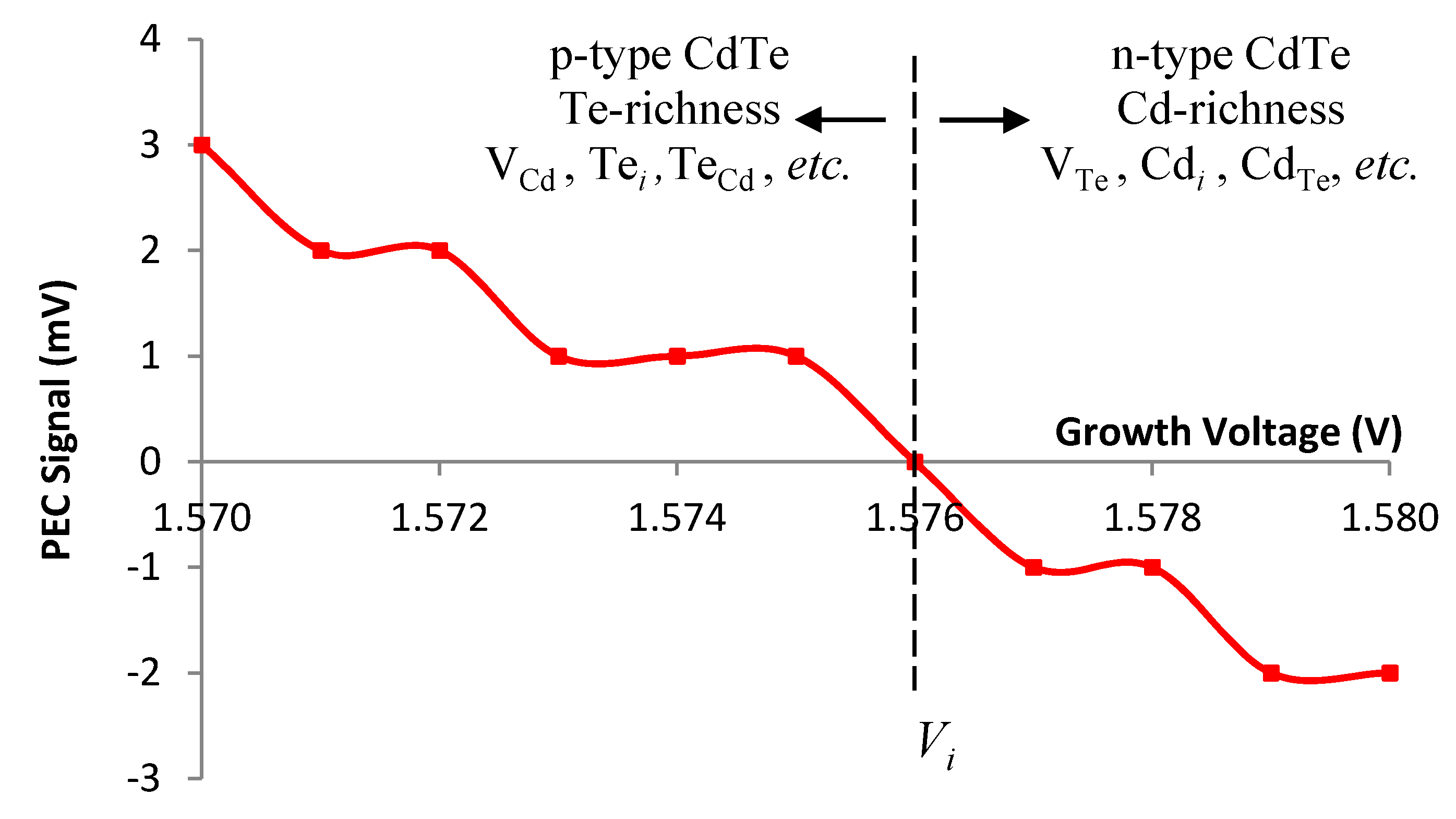
3.1. Ease of Growing Both n-Type and p-Type CdTe

The author’s group explores electrodeposition of semiconductors in details and it has been experimentally observed that both n-, i-, and p-type CdTe layers can be grown simply by varying the growth voltage [25,45]. A typical electrodeposition bath contains high concentration of Cd ions (0.5–1.5 M CdSO4) and low concentration of Te ions, together with 1000 ppm level of Cl. Electrodeposition has been carried out using a two-electrode system, and simply by changing growth voltage, p-type, i-type and n-type CdTe layers can be produced [25]. Figure 1 shows the variation of photoelectrochemical (PEC) signal for CdTe layers as a function of growth voltage. PEC signal is the open circuit voltage created at the solid/liquid (CdTe/Na2S2O3 aqueous solution) junction and is used to determine the electrical conduction type of a semiconducting layer. At low cathodic voltages (V < Vi—see Figure 1), the CdTe layers are Te-rich and p-type in electrical conduction. At higher cathodic voltages (V > Vi), the layers are rich in Cd and therefore n-type in electrical conduction. At the transition voltage Vi, the layer is stoichiometric, resistive and shows the highest crystallinity. These observations therefore strongly indicate the ease of production of CdTe in both n-type and p-type simply by changing the material composition. This also highlights the necessity of knowing the electrical conductivity type of CdTe before fabricating solar cells, in order to critically analyse experimental results and draw the right conclusions. Any growth technique could vary the Cd:Te ratio during the growth process simply by slight changes in growth parameters, and hence easily convert its electrical conduction type. This could create a huge confusion in interpretation of final results as it is now becoming clear from the reported results and new findings.
Figure 1. Photoelectrochemical (PEC) signal as a function of electrodeposition voltage for ED-CdTe layers grown in the vicinity of the stoichiometry point (Vi). Note the possible transition from p-type to n-type, due to Te-richness and Cd-richness. Most possible native defects within CdTe layers are also given in the two regions [25].
Coatings 04 00282 g001
The literature is rich in publications reporting the growth of both n-type and p-type CdTe [25,29,45]. As shown in Figure 1, the material can be converted into p- or n-type easily by changing the growth voltage by a few millivolts. Therefore, the defect distribution in CdTe can vary drastically by changing growth conditions. As shown in Figure 1, the materials grown at Vi have 50:50 (Cd:Te) stoichiometry, highest crystallinity and the lowest electrical conductivity. Cd-rich materials grown at cathodic voltages greater than Vi have defects of VTe, Cdi, CdTe, etc., and Te-rich materials grown at cathodic voltages less than Vi have defects of VCd, Tei, TeCd, etc. Heat treatment of materials grown in the vicinity of Vi can be converted from p to n and from n to p as demonstrated later in Figure 4, Figure 5 and Figure 6.

3.2. p-Type Doping by Chlorine Complexes

Recent cathodoluminescence (CL) results reported by Mazzamuto et al. [20] is worth discussing in detail, and these results are shown in Figure 2. The results were recorded for different CSS-CdTe layers grown, as a function of pressure of Freon gas inserted into the chamber during post-growth annealing process. The peak at 1.57 eV shows the band edge emission and the increase of CL peak at 1.40 eV is the most interesting. This peak grows as the concentration of Cl and F (halogens) increased in the annealing chamber. This means that these halogens introduce a defect or doping level very close to the valence band maximum making the material p-type. This is a key experimental observation to conclude that increased halogen concentration makes CdTe p-type. The presence of this peak at ~1.40 eV has been observed by few other research groups using PL and CL measurements [13,17,46].
Most of the researchers believe this to be a complex between VCd and Cl or F, but this seems to be another assumption in the PV field needing careful attention and rectification in order to understand this key processing step. This will be discussed in details in a later section of this paper.
Figure 2. Comparison of CL spectra acquired for (a) un-treated CSS-CdTe and treated CSS-CdTe in 400 mbar Ar, and HCF2Cl (Freon) atmosphere for 10 min using (b) 30 mbar, (c) 40 mbar and (d) 50 mbar Freon partial pressure [20].
Coatings 04 00282 g002

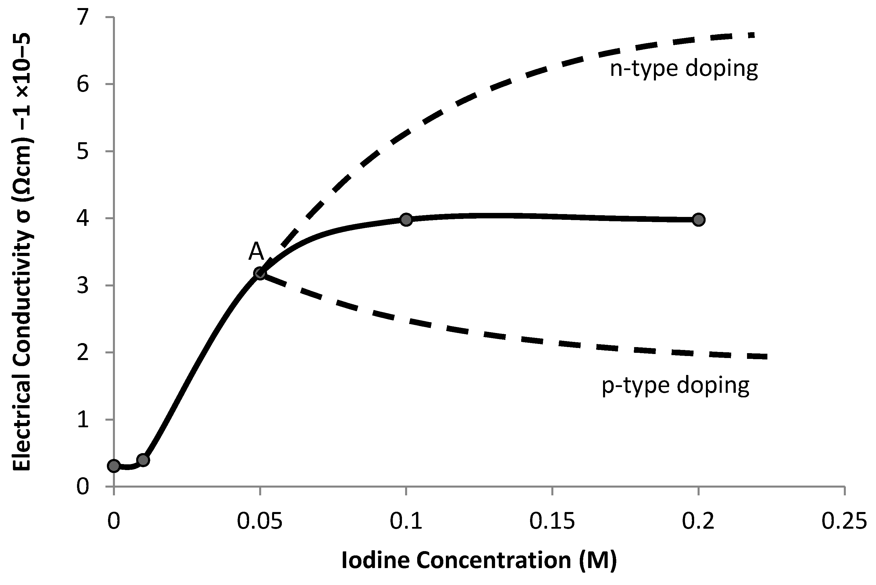
3.3. Variation of Electrical Conductivity

Halogen doping in CdTe needs careful observations and consideration. The group VII elements (halogens; F, Cl, Br, and I) are in general shallow donors in CdTe when group VI, (Te) atoms are replaced by group VII halogens [32,33]. However, the experimental observations described above show that Cl and F can also be p-type dopants. This amphoteric behaviour of halogens makes it more complex to understand the CdCl2 treatment. In fact both behaviours have been shown in previous experimental results published by the author’s group [31].
Figure 3 shows the variation of electrical conductivity (σ) as a function of iodine (I) concentration in the electrolytic bath, which contains Cl and I. While Cl concentration was constant, I concentration was gradually increased and the variation of σ was observed as given in Figure 3. At low I concentrations, σ increases due to n-type doping as a result of iodine behaving as a shallow donors. However, as the iodine concentration increased, σ saturates due to a triggering of p-doping mechanism at point A. After this point, there are two competing mechanisms to dope the material n-type and p-type, and therefore σ remains almost constant at ~3.9 × 10⁻⁵ (Ω·cm)−1. In this case, the behavior of I must be very similar to that of Cl or halogens in general. This constant conductivity must be the reason for good device performance, whatever the amount of CdCl2 used for CdCl2 treatment. This appears to be due to inherent self-compensation taking place in CdTe due to both n-type and p-type doping taking place simultaneously when sufficient amount of halogens is incorporated in CdTe. Fortunately, this natural amphoteric behavior of halogens is helping to produce a healthy device and avoiding device deterioration due to possible heavy doping of the material. It is also reported that I-doping of CdTe drastically reduces the mid-gap defect states [47], reducing recombination process, and, hence, helping to achieve high efficiency solar cell devices.
Figure 3. Typical variation of electrical conductivity (σ) of CdTe as a function of increasing iodine concentration in the electrolytic bath. Note the initial n-type doping and final saturation of σ, as a result of triggering of p-type doping at point A, due to high iodine concentration. Self-compensation mechanism sets the final conductivity at σ = 3.9 × 10⁻⁵ (Ω·cm)−1 (ρ = 2.6 × 10⁴ Ω·cm), producing semi-insulating CdTe layers.
Coatings 04 00282 g003
In this iodine doping experiment in the presence of Cl in the bath, the electrical conductivity increased only by a factor of ~10. Shah et al. [48] also reported the electrical resistivity drop by only a factor of ~20 in CdCl2-treated CdTe samples grown by CSS method.

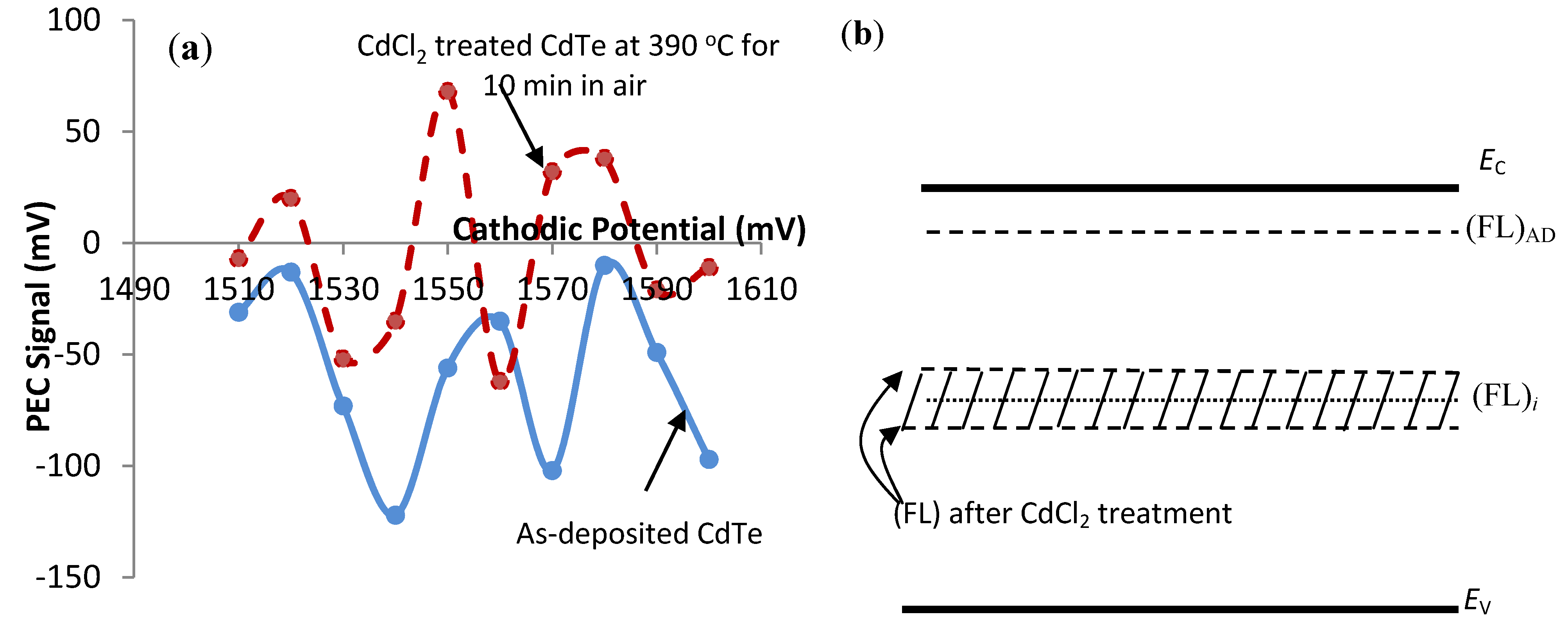
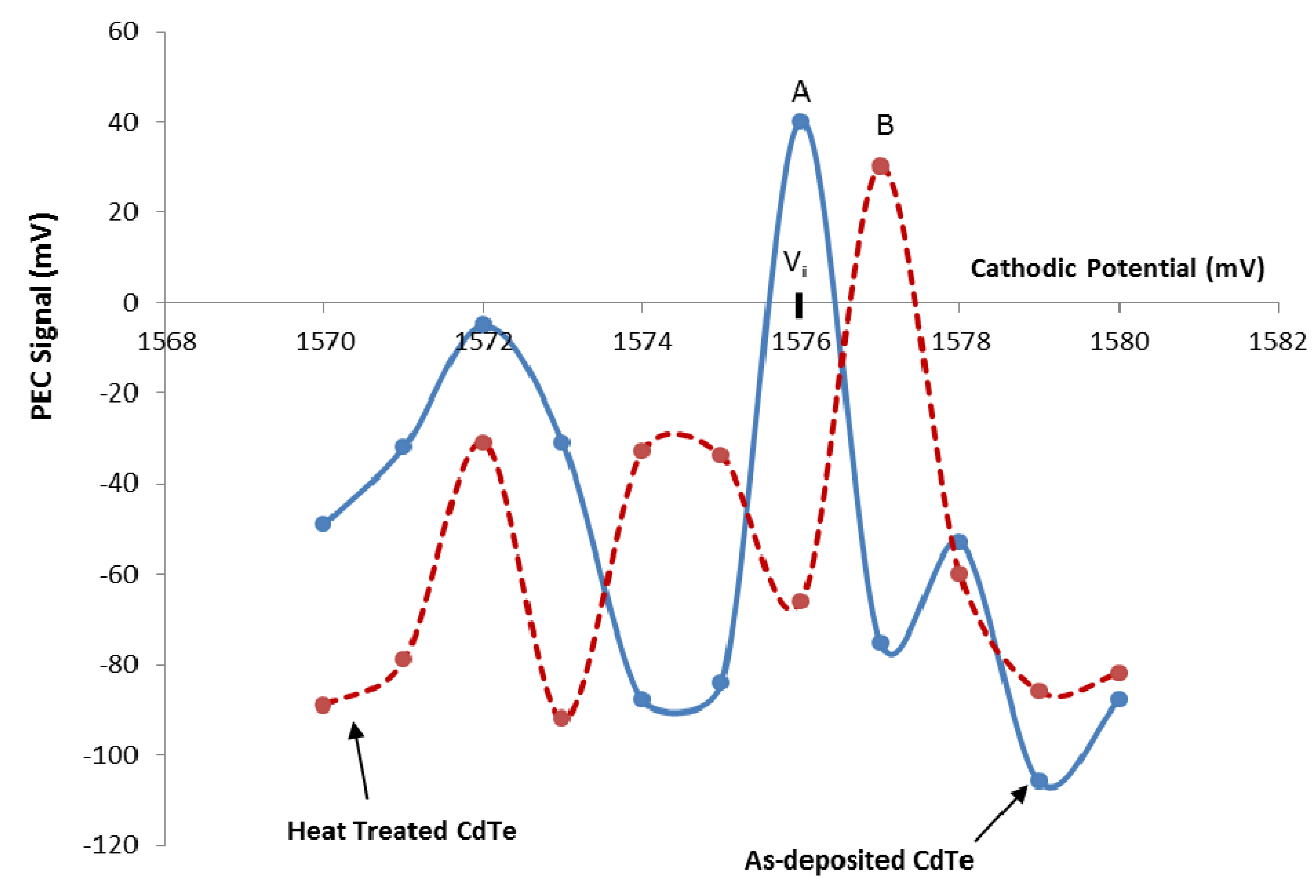
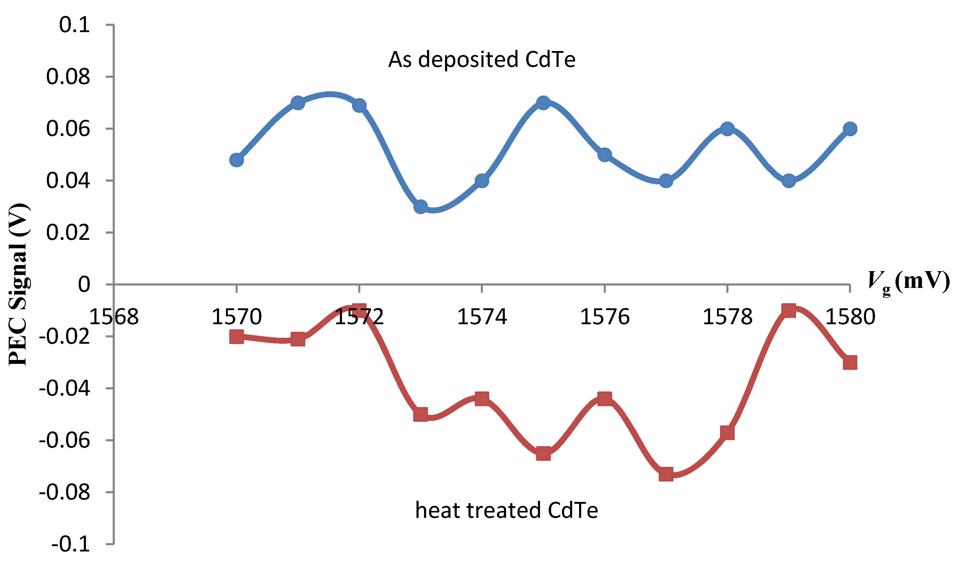
3.4. Photoelectrochemical (PEC) Cell Studies

PEC observations have been an invaluable method to determine the electrical conduction type of thin semiconducting films grown on glass/FTO substrates. Conventional Hall Effect measurements cannot be performed due to the underlying conducting FTO layer, unless the layer is transferred to an insulating support, which is extremely difficult, destructive and time consuming. Therefore the PEC has been successfully applied to fulfill this purpose. This is by forming a depletion layer at solid/liquid junction and measuring its open circuit voltage under illumination [37]. The sign of the PEC signal determines the electrical conduction type and the magnitude of the PEC signal qualitatively indicates the suitability of doping concentration in the semiconducting material.
Figure 4a shows the PEC signals for ten CdTe layers electrodeposited at different voltages. These as-grown layers are all n-type, but when CdCl2-treated, the PEC signals show the changes towards p-type CdTe. This observation clearly indicates the trend of moving from n-type towards p-type conduction. In other words, the doping concentration changes from high n-type towards low n-doping or intrinsic values and then to p-type CdTe. This is mainly due to re-distribution and annealing-out of defects in the material layers. The material’s doping concentration changes, but could remain as n-type, i-type, or convert to p-type during this heat treatment depending on the defect structure present in the starting material. In this particular set of 10 samples, four samples converted to p-type while the other six samples remained as n-type layers. In fact two of the six samples reached almost zero PEC values becoming semi-insulating or insulating CdTe materials.
Figure 4. (a) Typical variation of the PEC signal when CdTe undergoes CdCl2 treatment and (b) the corresponding FL positions before and after CdCl2 treatment.
Coatings 04 00282 g004
These results enable us to visualise the movement of the Fermi Level (FL) in the bandgap during this CdCl2 treatment. Figure 4b shows the position of the FL with respect to the two main energy band edges, Ev and Ec. For intrinsic CdTe, the FL should be in the middle (~0.72 eV above the Ev) of the forbidden bandgap. As deposited CdTe layers show large negative PEC signals in the order of 100 mV, and therefore the material is n-type and the (FL)AD should be in the upper half of the bandgap close to Ec as shown in Figure 4b. CdCl2 treatment reduces the magnitude of the negative PEC signal and changes the material towards p-type conduction. This means that the FL moves towards the middle of the bandgap and enters the shaded region in the vicinity of (FL)i, giving rise to insulating material. For four samples out of this set, the FL has crossed to the lower half of the bandgap becoming p-type in electrical conduction. This FL variation is clear as a function of CdCl2 treatment and can be translated into the variation of doping concentration in the material. This means that the as-deposited layers have high excess donor concentration (NDNA), but with CdCl2 treatment, NA increases gradually reducing (NDNA), bringing the CdTe closer to intrinsic material (NDNA). Depending on the doping concentrations, the layer, therefore, becomes p-type when NA > ND. The doping concentration is then (NAND) and the layer is p-type. It is also indicating that high-performing CdTe solar cell material has semi-insulating properties and the FL lies close to the middle of the band gap. A large body of experimental results produced in the author’s group shows that high efficiency solar cells are formed when the material is n-type rather than p-type [34,35]. This information has also been reported by Schulmeyer et al. by investigating the relationship between the efficiency and the position of the Fermi Level (FL) in the bandgap [49]. These authors show that high efficiency is achieved when the FL is situated above the midgap of CdTe, i.e., when the material is low n-doped. A similar conclusion was also drawn by Bayhan et al. [30] by doping CdTe p-type using the p-type dopant, Sb. The improvement of devices by trial and error method could therefore finally settle down with high efficiency devices based on n-type CdTe layers, and if the interpretations are based on a simple p-n junction device, it creates confusion rather than enlightenment.
The results shown in Figure 5 also bring important information to this discussion. This represents the PEC signal of another set of CdTe layers grown as a function of growth voltage. Vi represents the inversion voltage and produces stoichiometric CdTe layers when the pH of the electrolyte is 2.00 ± 0.02. When the materials are grown close to this point, and heat-treated with CdCl2 treatment, defect re-distribution takes place and the shift can be either way due to the final set of defects and hence the doping concentration. Here, the sample-A converts from p-type to n-type, and sample-B converts from n-type to p-type. In the past, n-type to p-type conversion was always assumed in discussing and interpreting CdS/CdTe solar cells, but this is not always the case. The general trend is to reduce the n-type doping concentration towards that of i-CdTe and some layers completely transform into p-type. However, when close to the inversion point, the material layers transform from p-type to n-type as well. There are several reports in the literature on the p-type to n-type conversion of CdTe layers [50,51]. This again highlights the importance of knowing the right electrical conduction type of CdTe layer before fabricating solar cells and interpreting device results.
As another example, Figure 6 shows the p-type nature of a set of 11 as-deposited CdTe layers. When heat-treated in air, without CdCl2 treatment, all the samples become n-type in electrical conduction from their initial p-type electrical conduction. Therefore, there is no specific trend of type conversion, but this strongly depends on the initial material as well as its impurity and defect structure due to native imperfections present.
Figure 5. PEC signals observed before and after heat treatment in air (without CdCl2 treatment) for a set of electrodeposited CdTe layers grown in the vicinity of the stoichiometric voltage (Vi). Moving towards p-type is less than when CdCl2 is present, but note the sample A, turning from p- to n-, and sample B, turning from n- to p-, after heat treatment in air. When close to the intrinsic point, transition in both directions is possible since NAND. Defect re-distribution could change the electrical conductivity in either direction.
Coatings 04 00282 g005
Figure 6. A set of electrodeposited p-type CdTe, and their type conversion to n-type after heat treatment in air, without CdCl2 treatment.
Coatings 04 00282 g006

3.5. Columnar Growth of CdS and CdTe

Different research groups use varying thicknesses for CdS and CdTe layers to fabricate thin film solar cells. The thickness used for CdS varies from 10–50 nm [9] to 1–2 µm [10]. Similarly the CdTe layer thickness varies from 1.5 to 8.0 µm [9,11,12]. Therefore, the thinnest device is only ~1.5 µm thick and arises in the case of electroplating which is the growth method used by the author’s group. In this case and every other situation with thinner layers, surface and interface morphologies play a crucial role in device performance. If the layers are not grown in layer-by-layer mode, the structure will be full of pinholes and gaps, and therefore the back electrical contact will easily reach the front contact thereby short-circuiting the device. New experimental observations are presented below in order to highlight the importance of morphology.
Figure 7a shows the SEM picture of a thin layer of electroplated CdS. It is clear that the layer is not uniform and does not completely cover the FTO substrate. In the past, depending on the 2D-SEM, CdS layer was understood as a thin layer consisting of grains with ~20 nm diameter [9]. However, as a result of the spiky nature of FTO surface and the application of a constant voltage to this surface during electroplating, high electric fields exist at the FTO spikes. Therefore, CdS nucleates at these points and grow as columns normal to the substrate. As a result, CdS layer does not uniformly cover the FTO layer, until very thick layers are formed.
The electrodeposition of CdTe on glass/FTO/ED-CdS substrates covers some of the gaps but as shown in Figure 7b, pinholes still exist in the CdTe layer. Scientific literature, reports columnar growth [29] of CdTe, but electrodeposition enhances this growth pattern. This situation can be changed to a certain extent by using both thick CdS and CdTe layers. But in techniques such as electroplating, and in materials reduction efforts, the layers are extremely thin with CdS ~50–100 nm and CdTe ~1.5 µm and therefore other methods should be employed to overcome these issues. This is where the buffer layers are necessary to reduce pinholes, and pinhole-plugging layers are essential for covering remaining pinholes in this device, especially when very thin layers are used.
Figure 7. Typical 2D-SEM images of (a) electrodeposited CdS on glass/FTO substrate and (b) electrodeposited CdTe on glass/FTO/CdS substrate.
Coatings 04 00282 g007
Columnar type materials or nano- and micro-rods introduce both advantages and disadvantages to the research and development of thin film CdTe solar cells. The electroplated materials naturally grow as rods due to nucleation at spikes of FTO where high electric fields are present. These rods have near-perfect crystalline nature [52], and, therefore, the charge carrier mobilities along these nano-rods have highest possible values. In addition, the grain boundary scattering becomes minimal during PV activity across the device structure. However, the disadvantage is the formation of pinholes across the device due to the columnar shapes of these rods normal to the substrate. There are therefore two ways to progress; keeping the columnar nature, but using a suitable method to plug pinholes, or changing the growth behavior to avoid rod-like grain formation. We believe that our repeatedly observed, excessively high Jsc values arise due to these properties in CdS/CdTe devices [2,31,53]. Alternatively, the buffer layers can be used to change the growth mode of CdS from nano-rods to layer-by-layer mode, reducing pinhole formation. In this case, the advantages introduced by columnar shaped materials are lost in device performance. Both routes should be followed in this case to explore and establish a reproducible and consistent device structure. One method will be better than the other for achieving high efficiencies, and the research should be directed towards finding the best method. While ED-CdS grains tend to form columnar-type materials preferentially, CBD-CdS particles deposit on FTO surface uniformly, covering the surface completely. In this respect, CBD-CdS is more suitable for avoiding pinholes in the CdS layer.

4. Critical Discussion of Reported and New Results

This section combines the summary of results reported in Section 2, together with new key observations presented in Section 3. The key issues are then raised, critically analysed and discussed in order to contribute to better understanding of the CdCl2 treatment.

4.1. Grain Growth

The above summary of reported results clearly shows that the presence of Cl or halogens in general, helps in grain growth process by acting as a fluxing agent. This reduces the number of grain boundaries and therefore the density of defects, in addition to reducing the scattering of charge carriers at grain-boundaries within the material. This helps in improving the electrical properties of CdCl2-treated layers. What is interesting to note is that, even when the initial CdTe layer has large grains and there is no apparent grain growth, the effect of CdCl2 treatment on device performance is still helpful and drastic. Therefore, this indicates the presence of other key important improvements during this processing step in addition to grain growth. While the grain growth trend is widely accepted, establishment of correct doping levels for devices, defect passivation and reduction of pinholes could be the most effective processes taking place during CdCl2 treatment and should be thoroughly investigated.

4.2. Effects of Oxygen and Cd

In addition to the effect of Cl, oxygen and Cd seem to play very important roles. The results reported in the literature clearly show that CdCl2-treated materials (in the absence of oxygen) produce comparatively low device parameters [36]. Researchers have gone to build equipment to carry out CdCl2 treatment in the UHV conditions [49]. The results show that highest efficiencies achieved for ANTEC-CdTe material is ~9% in the absence of O2, compared to much higher values when the CdCl2 treatment is carried out in the presence of O2. Therefore, CdCl2 treatment in the presence of O2 seems to be the best condition. O2 may introduce CdO into CdS and CdTe layers, and completely change the wetting properties, growth behavior, or electrical properties of these layers. CdO is known to have n-type conduction and almost similar bandgap (2.20 eV) to CdS (2.42 eV) and hence could introduce useful results to the device [29].
The effect of large amounts of Cd in the form of CdCl2 during heat treatment of CdTe layer is not considered and discussed in the past. The presence of excess Te and Te precipitation is a natural occurrence in CdTe and Cd must be converting these excess Te into CdTe and thus improving the stoichiometry of the layers. The X-ray and γ-ray detector development community has done deep research in this area, showing the reduction of Te-precipitation by CdCl2 treatment [40,41,42]. However, the PV community has not taken up this knowledge to date for research and discussion of CdCl2 treatment.
All CdCl2 treatments are carried out in the presence of thick CdCl2 layers, but the discussions are always on complexes of Cl and Cd-vacancies (VCd-Cl). In the case of CdCl2 treatment, Cd-rich environment is present and therefore Te-vacancies (VTe) should be present in these layers rather than Cd-vacancies. Hence the complexes between Cl and Te-vacancies (VTe-Cl) could be the most possible p-type dopant rather than the complexes between Cd-vacancies and Cl (VCd-Cl), which are said to be created during CdCl2 treatment. This issue must be critically examined and explored in order to understand the CdCl2 treatment.

4.3. Interactions at CdS/CdTe Interface

Soft-XPS studies on numerous interfaces between inorganic semiconductors show that these interfaces undergo chemical reactions, alloying as well as in- and out- diffusion of semiconductor constituent atoms, even below room temperature [54]. Therefore CdS/CdTe is not an exception and all these interactions are expected during growth, heat treatment and ageing. There are several publications in the literature reporting the experimental observation of CdSxTe(1−x) phase at the interface [10,17,24]. This formation of intermediate material is helpful in creating a gradual energy band gap transition from 2.42 eV (Eg of CdS) to 1.45 eV (Eg of CdTe), producing a graded bandgap hetero-junction and therefore enhancing the internal electric field of the device which helps in charge carrier separation and collection. It is interesting to note the beneficial effects when CdS layer thickness is reduced down to extremely low values of 10–50 nm [9]. In this case CdS must be fully absorbed into the CdTe layer, and CdS is simply providing a better nucleation environment for device quality CdTe layer to grow. It is also relevant to note that Das and Morris [55] reported superior devices without CdS in compared to their devices with CdS. They must have used a good cleaning process for the TCO in order to grow device quality CdTe in their experiments. In this case researchers should question where the PV active junction is. According to the author’s understanding in 2002 [2], after a long exposure to CBD-CdS/Electroplated CdTe structure, this device is a combination of n-n hetero-junction and a large Schottky barrier at the back contact. After another decade, it is becoming clear that there are two types of solar cells under research and development. Some groups are working on genuine p-n junction devices and others on n-n hetero-junction and a large Schottky barrier at the back contact. The device must be identified first in order to analyse and describe results accurately. Confusions raised by researchers can be explained by identifying this difference.

4.4. Surface Roughness

Increase in surface roughness is practically not helpful for a thin film solar cell device especially as it regards making effective electrical back contacts. However, the use of thick electrical contacts can remove this disadvantage. The formation of large and columnar grains helps in charge carrier transport normal to the substrate during PV action by minimizing scattering due to grain boundaries. This will help in maximising charge carrier mobility thus enhancing the performance of the device. It should be noted that Hall mobility measured parallel to the substrate for CdTe thin films can be two or three orders of magnitude low, when compared to the electron conduction, normal to the substrate, along columns or within single grains. The reason is the vast difference in electron scattering taking place during electron transport parallel to the substrate due to crossing of grain boundaries in the material by electrons. The electrons transporting normal to the substrate, during PV action, experience minimum scattering when compared to electrons transporting parallel to the substrate during Hall Effect measurements, which experience maximum scattering due to crossing of large numbers of grain boundaries. Therefore, the Hall mobilities reported in the literature for CdTe polycrystalline layers do not represent the mobility of photo-generated charge carriers during PV action. The mobility of charge carriers during PV action can be a few orders of magnitude higher than the Hall mobility parallel to the substrate.

4.5. Lifetime of Charge Carriers

Enhancement of lifetime of charge carriers is most important in increasing device performance. The possible reasons could include reduction of grain boundaries, passivation of detrimental native defects, reduction of recombination, etc. Improved lifetime of photo-generated charge carriers enables their effective separation and transfer to respective electrical contacts, before their recombination. It is experimentally shown that inclusion of iodine in CdTe drastically reduces mid-gap “Killer Centres” [47] and therefore helps in the improvement of charge carrier lifetime and improvement of device parameters. All halogens (F, Cl, I) studied to date seem to have this property and therefore CdCl2 treatment creates similar situation.

4.6. Doping Concentrations

In order for thin film PV devices to work, the most important thing to do should be to build a healthy depletion region across the device structure. Typical CdS/CdTe thin film solar cell has a thickness of ~2 µm to ~8 µm, according to current research, and the ideal scenario is that the depletion region thickness should be approximately equal to the thickness of the CdS/CdTe structure. In order to have a depletion region of ~2 µm, the doping concentration of CdTe should be ~1.0 × 1015 cm−3 [56]. For a device with ~8 µm, the doping concentration should be further reduced to ~1.0 × 1014 cm−3 or below. In this case, the full device thickness is covered by the depletion region thus producing a fully depleted device and the whole thickness is PV active. In other words, the internal electric field exists across the entire thickness making the device more effective. Careful observation of the published results in the literature show that, high efficiency devices (say >10%) have doping concentrations in the range of ~1.0 × 10¹⁴ to ~5.0 × 1015 cm−3 [57,58,59,60]. Therefore, by the various improvements mentioned above, the CdCl2 treatment incidentally sets the doping concentration to this most important range producing efficient devices. It is surprising to see that this right doping concentration is set up by the CdCl2 treatment, without any dependence on the concentration of Cl used in the CdCl2 treatment. It can be recalled that there seems to be two competing doping processes taking place during this processing step, as mentioned earlier. Halogens (F, Cl and I) seem to be acting as both n-type and p-type dopant simultaneously (amphoteric behavior) in CdTe, setting up the right doping concentration for this device. One process is the normal n-doping of halogens by replacing Te atoms at lower halogen concentrations. The second process seems to be the “anomalous” complex formation between the halogens and an unknown native defect in CdTe. This anomalous p-type doping process is triggered when high concentrations of halogens are incorporated into CdTe as shown by the results in Figure 3. This native defect that facilitates p-type doping needs to be experimentally identified, in order to fully understand CdCl2 treatment, and this has been discussed in Section 4.2. Suitable experiments are necessary to investigate the doping concentration before and after the CdCl2 treatment to confirm this and strengthen our understanding in this processing step.

4.7. Preventing Device Leakage

Grain boundaries and un-filled gaps (pinholes) provide easy paths for the two electrical contacts to short-circuit the device. Therefore, it is important to electrically passivate these paths and mechanically block these pinholes. Therefore, there are two paths to follow; encouraging columnar type layers to grow in a compact way and establishing an effective pinhole plugging process, or encouraging layer-by-layer growth by avoiding columnar-type material formation and therefore removing pinhole formation. In the latter case, buffer layers are essential to change the natural nucleation and growth behaviour of CdS and CdTe. Avoidance of pinhole formation by using buffer layers, and plugging of remaining pinholes are necessary in order to develop highly efficient thin film solar cells. In order to fabricate a robust solar cell therefore, 4-layer device structures should be established by incorporating buffer and pinhole plugging layers to the basic CdS/CdTe structure. This approach is more appropriate for CdS/CdTe devices with lower thicknesses.

4.8. Dealing with n- and p-Type CdTe

The large body of experimental results and new findings show the existence of CdTe in both n- and p- type electrical conduction types. Doping of CdTe seems to be affected by (i) composition of the material; (ii) effects of shallow dopants by replacement of host atoms (n-doping by Group-VII and Group-III elements and p-doping by Group I and V elements) and (iii) p-type doping due to formation of complexes between halogens and a native defect. Equal amounts of Cd and Te produce stoichiometric, highly crystalline, resistive and i-type CdTe, and slight richness in Te and Cd produces p-type and n-type CdTe respectively. Addition of external dopants and impurity incorporation during growth or processing can also convert the material into n- or p-type conduction type. In addition, self-compensation takes place easily in this material due to formation of complexes between halogen and native defects. It has also been experimentally shown that the heat treatment in air or CdCl2 treatment changes the doping concentration of this material. In general, these treatments reduce the n-doping concentration and take the material to i-type or p-type region. When the material is close to i-type, it can change from n- to p- or p- to n- depending on the defects and impurity distribution in the layers.
With all the above possibilities, CdTe layers used to make CdS/CdTe solar cells have been assumed as p-type in electrical conduction most of the times. This certainly has led to contradicting and confusing conclusions and therefore future R&D programmes need to experimentally check the starting material’s conduction type before the interpretation of experimental results. The ease of CdTe material’s presence in both n- and p-type conduction types has created a very complex situation.
A good example is the work by T Schulmeyer et al. [49], in which they have measured the FL position by photoemission technique. These authors worked on ANTEC-CdTe, measuring the FL movement in the bandgap as a function of CdCl2 treatment, and confirmed that high efficiency solar cells were obtained when the FL is 0.85 eV above the Ev. That is, when the material is n-type in electrical conduction compared to when it is p-type in electrical conduction. This material was p-type before CdCl2 treatment and the FL moved upwards to ~Ev + 0.85 eV during CdCl2 treatment. Clearly the material became semi-insulating and n-type, and produced high efficiencies. In their own words, the authors concluded by stating: “This surprising result does not correspond to the accepted model of the device physics of the CdS/CdTe solar cell”. This indeed confirms the requirement of deep understanding of the physics of this device before its further development. Now it is clear that the two types of devices are present in the field of CdTe solar cells grown by other methods as well. It should be noted that the mobility of electrons are much higher in n-type CdTe (~1000 cm2·V−1·s−1) than the mobility of holes in p-type CdTe (~20–80 cm2·V−1·s−1) and therefore leads to both high charge carrier movement and high device performance in devices with n-CdTe.
Unless this CdS/CdTe device is researched with open mindedness, the manufacturing process will experience reproducibility and yield issues in the future. Once fully understood, this device is capable of entering into mid −20% efficiency region, breaking the stagnation observed in the past few decades.

5. Toxicity and Availability of Cd and Te Elements

It is also relevant to discuss briefly the toxicity and availability of both Cd and Te elements. Cd is a heavy metal, well known as a toxic material. However, the world produces over 22,000 metric tons of Cd today as a by-product of Cu and Zn refinement [61]. A good fraction of this Cd is used in Ni-Cd batteries and the rest could severely pollute the environment if not managed properly. Once Cd is chemically reacted with S and Te, CdS, and CdTe stable compounds are formed. These are less toxic and in the past, these compounds have been used as pigments. Therefore, the smartest way to utilise already produced Cd is to convert Cd into less toxic CdS and CdTe, fabricate CdS/CdTe solar panels and produce clean energy, minimising CO2 emission. Therefore manufacturing CdS/CdTe solar panels becomes an excellent way to manage large amounts of Cd already being produced as a by-product. At the same time, solar PV manufacturers are arranging to re-cycle solar panels at the end of their lifetime to protect the environment.
Another concern is the availability of adequate Cd and Te to move forward for large scale manufacturing of CdS/CdTe solar panels. Concerns are more critical for Te element, for its scarcity compared to cadmium. This analysis has been carried out by Zweibel [62] in detail, and the reader is directed to his critical analysis. As a solution to this issue, the scientific research should be directed towards extremely thin CdTe layers (~0.60 µm) instead of ~2.00 µm thick layers.

6. Concluding Remarks and Further Studies Required

The summary of reported results, the new experimental evidence and critical discussion above suggest that it is necessary to carry out systematic and key investigations in order to fully understand the CdCl2 treatment of CdTe. The following areas are the most important for future research in order to elucidate the mechanisms taking place during this crucial processing step.

6.1. Phase Transition Observed in CdTe Layer

There is need to establish whether the (111) highly oriented CdTe films or randomly oriented CdTe films showing several strong peaks with comparable intensities produce the highest solar cell efficiencies. This structure-property relationship is an essential knowledge to establish in CdTe solar cell development. There are indications that the CdTe layer undergoes a structural phase transition close to 385 °C.

6.2. Conductivity Type of CdTe before Fabricating Devices

The research work should start by determining the electrical conduction type of the starting CdTe layer. Assumptions are not adequate since the electrical conduction type can change during the growth process due to composition change, addition of any dopants during the growth and processing, and self-compensation effects. CdTe can easily become n- i- or p-type depending on the composition changes and heat treatment after CdCl2 treatment. The interpretations given without knowing the exact electrical conductivity type of the material, can lead only to drawing inaccurate and confusing conclusions.

6.3. Effects of Oxygen and Cd

Scientific literature indicates that the CdCl2 treatment in the presence of oxygen produces better devices. The inclusion of oxygen in the material and device structure should be examined in a systematic way in order to understand this processing step. The effect of excessive Cd in removal of Te-precipitation in CdTe is important and deserves comprehensive research. This has not been considered or discussed in the CdTe solar cell development programmes.

6.4. Changing of Doping Concentration

The electrical conductivity variation and doping concentration variation should be explored carefully in order to examine and understand CdCl2 treatment. The final performance of the fully fabricated devices depends on the doping concentration of CdTe. However, systematic doping concentration measurements before and after CdCl2 treatment are rare in the literature.

6.5. Defects in CdS and CdTe

The defects in both CdS and CdTe layers play a crucial role in determining efficiency of CdS/CdTe solar cells. Therefore, suitable techniques should be used in a comprehensive way in order to study the defects mapping of these two materials. The study of defects in a narrow energy range is not helpful but the defects mapping throughout the band gap of CdS and CdTe will be extremely useful. Only a few defect levels will dominate in deciding the electrical properties of the device, and these dominating defect levels should be identified.

6.6. Microscopic Current Collection

The role of columnar-type material layers and therefore enhanced grain boundary charge collection should be explored in detail to understand the CdCl2 treatment in CdTe solar cell development [63]. Recent work shows that solar cells with excessively high Jsc values [2,31,34,35] arise due to involvement of columnar type material grains in the device structure. The effect of doping at grain boundaries should be explored using techniques such as electron beam induced current (EBIC), and the use of buffer layers and pinhole-plugging layers should be thoroughly investigated in order to unravel and understand the secrets behind this device and improve its conversion efficiency to higher values, beyond 20%.

Acknowledgments

The author would like to thank and acknowledge the contributions made by C. J. Blomfield, S. M. McGregor, A. P. Samantilleke, N. B. Chaure, Jayne Wellings, G. Muftah, D. G. Diso, A. R. Weerasinghe, P. A. Bingham, O. K. Echendu, F. Fauzi, H. I. Salim, N. A. Abdul-Manaf, O. I. Olusola and M. L. Madugu. The collaborating teams in Italy (Nicola Romeo and Allesio Bosio) and in USA (Thad Druffle and Ruvini Dharmadasa) are gratefully acknowledged for their contributions through discussions on new findings. Although a limited number of references have been cited in this paper, the author wishes to acknowledge and thank many scientists who contributed to this area of research over the past three decades. Gareth Roberts (Late), Mike Petty, Robin Williams and Emeric Rhoderick are gratefully acknowledged for their guidance during the author’s early stage of scientific research to develop in this field.

Conflicts of Interest

The author declares no conflict of interest.

References

  1. Wesoff, E. First Solar on the Future of Photovoltaics: Part 2. In order to thrive, First Solar must deploy 65 GW of photovoltaic panels over the next decade. Available online: http://www.greentechmedia.com/articles/read/First-Solar-on-the-Future-of-Photovoltaics-Part-2/ (accessed on 20 March 2014).
  2. Dharmadasa, I.M.; Samantilleke, A.P.; Young, J.; Chaure, N.B. New ways of developing glass/conducting glass/CdS/CdTe/metal thin-film solar cells based on a new model. Semicond. Sci. Technol. 2002, 17, 1238–1248. [Google Scholar] [CrossRef]
  3. Green, M.A.; Emery, K.; Hishikawa, Y.; Warta, W.; Dunlop, E.D. Solar cell efficiency tables (version 42). Prog. Photovolt. Res. Appl. 2013, 21, 827–837. [Google Scholar]
  4. First Solar CdTe 18.7% Efficient Cell Breaks Record. Compound Semiconductor Website. Available online: http://www.compoundsemiconductor.net/csc/news-details/id/19736074/name/First-Solar-CdTe-18.7-efficient-cell-breaks-recor.html (accessed on 20 March 2014).
  5. First Solar Sets World Record for CdTe Solar Cell Efficiency. First Solar Website. Available online: http://investor.firstsolar.com/releasedetail.cfm?ReleaseID=828273 (accessed on 20 March 2014).
  6. First solar sets CdTe module efficiency world record, launches series 3 black module. Available online: http://investor.firstsolar.com/releasedetail.cfm?releaseid=755244 (accessed on 5 June 2013).
  7. Nakayama, N.; Matsumoto, H.; Yamaguchi, K.; Ikagami, S.; Hioki, Y. Ceramic thin film CdTe solar cell. Jan. J. Appl. Phys. 1976, 15, 2281–2282. [Google Scholar] [CrossRef]
  8. Fritsche, J.; Gunst, S.; Golusda, E.; Lejard, M.C.; Thißen, A.; Mayer, T.; Klein, A.; Wendt, R.; Gegenwart, R.; Bonnet, D.; et al. Surface analysis of CdTe thin film solar cells. Thin Solid Films 2001, 387, 161–164. [Google Scholar] [CrossRef]
  9. Razykov, T.M.; Ferekides, C.S.; Morel, D.; Stefanakos, E.; Ullal, H.S.; Upadhyaya, H.M. Solar photovoltaic electricity: Current status and future prospects. Solar Energy 2011, 85, 1580–1608. [Google Scholar] [CrossRef]
  10. McCandless, B.E.; Birkmire, R.W. Analysis of post deposition processing for CdTe/CdS thin film solar cells. Solar Cells 1991, 31, 527–535. [Google Scholar] [CrossRef]
  11. Caraman, I.; Vatavu, S.; Rasu, G.; Gaşin, P. The luminescence of CdS and CdTe thin films, components of photovoltaic cells. Chalcogenide Lett. 2006, 3, 1–7. [Google Scholar]
  12. Romeo, N.; Bosio, A.; Tedeschi, R.; Romeo, A.; Canevari, V. A highly efficient and stable CdTe/CdS thin film solar cell. Solar Energy Mater. Solar Cells 1999, 58, 209–218. [Google Scholar] [CrossRef]
  13. Metzger, W.K.; Albin, D.; Romero, M.J.; Dippo, P.; Young, M. CdCl2 treatment, S diffusion, and recombination in polycrystalline CdTe. J. Appl. Phys. 2006, 90. [Google Scholar] [CrossRef]
  14. Jahn, U.; Okamoto, T.; Yamada, A.; Konagai, M. Doping and intermixing in CdS/CdTe solar cells fabricated under different conditions. J. Appl. Phys. 2001, 90, 2553–2558. [Google Scholar] [CrossRef]
  15. Komin, V.; Tetali, B.; Viswanathan, V.; Yu, S.; Morel, D.L.; Ferekides, C.S. The effect of the CdCl2 treatment on CdTe/CdS thin film solar cells studied using deep level transient spectroscopy. Thin Solid Films 2003, 431–432, 143–147. [Google Scholar]
  16. Compann, A.; Bhat, A. Laser-driven physical vapor deposition for thin-film CdTe solar cells. Int. J. Sol. Energy 1992, 12, 155–169. [Google Scholar] [CrossRef]
  17. Potter, M.D.G.; Halliday, D.P.; Cousin, M.; Durose, K. A study of the effects of varying cadmium chloride treatment on the luminescent properties of CdTe/CdS thin film solar cells. Thin Solid Films 2000, 361–362, 248–252. [Google Scholar]
  18. Romeo, A.; Bätzner, D.L.; Zogg, H.; Tiwari, A.N. Recrystallization in CdTe/CdS. Thin Solid Films 2000, 361–362, 420–425. [Google Scholar]
  19. Cunningham, D.; Rubcich, M.; Skinner, D. Cadmium telluride PV module manufacturing at BP Solar. Prog. Photovolt. 2002, 10, 159–168. [Google Scholar] [CrossRef]
  20. Mazzamuto, S.; Vailant, L.; Bosio, A.; Romeo, N.; Armani, N.; Salviati, G. A study of the CdTe treatment with a Freon gas such as CHF2Cl. Thin Solid Films 2008, 16, 7079–7083. [Google Scholar]
  21. Peter, L.M.; Wang, R.L. Channel flow cell electrodeposition of CdTe for solar cells. Electrochem. Commun. 1999, 1, 554–558. [Google Scholar] [CrossRef]
  22. Moutinho, H.R.; Al-Jassim, M.M.; Abufoltuh, F.A.; Levi, D.H.; Dippo, P.C.; Dhere, R.G.; Kazmerski, L.L. Studies of recrystallization of CdTe thin films after CdCl2 treatment [Solar cells]. In Proceedings of 26th IEEE Photovoltaic Specialists Conference (PVSC), Anaheim, CA, USA, 29 September–3 October 1997; pp. 431–434.
  23. Rami, M.; Benamar, E.; Fahoume, M.; Chraibi, F.; Ennaoui, A.M.J. Effect of heat-treatment with CdCl2 on the electrodeposited CdTe/CdS heterojunction. Condens. Matter. 2000, 3, 66–70. [Google Scholar]
  24. Paulson, P.D.; Dutta, V. Study of in situ CdCl2 treatment on CSS deposited CdTe films and CdS/CdTe solar cells. Thin Solid Films 2000, 370, 299–306. [Google Scholar] [CrossRef]
  25. Diso, D.G. Research and development of CdTe based thin film PV solar cells. Ph.D. Thesis, Sheffield Hallam University, Sheffield, UK, October 2011. [Google Scholar]
  26. Schaffner, J.; Motzko, M.; Tueschen, A.; Swirschuk, A.; Schimper, H.-J.; Klein, A.; Modes, T.; Zywitzki, O.; Jaegermann, W. 12% efficient CdTe/CdS thin film solar cells deposited by low-temperature close space sublimation. J. Appl. Phys. 2011, 110, 064508:1–064508:6. [Google Scholar]
  27. Lee, J. Effects of heat treatment of vacuum evaporated CdCl2 layer on the properties of CdS/CdTe solar cells. Curr. Appl. Phys. 2011, 11, S103–S108. [Google Scholar] [CrossRef]
  28. Kim, M.; Sohn, S.H.; Lee, S.H. Reaction kinetics study of CdTe thin films during CdCl2 heat treatment. Solar Energy Mater. Solar Cells 2011, 95, 2295–2301. [Google Scholar]
  29. Chu, T.L.; Chu, S.S. Thin film II–VI photovoltaics. Solid State Electron. 1995, 38, 533–549. [Google Scholar] [CrossRef]
  30. Bayhan, H.; ErÇelebi, C. Effects of post deposition treatments on vacuum evaporated CdTe thin films and CdS/CdTe heterojunction devices. Tr. J. Phys. 1998, 22, 441–451. [Google Scholar]
  31. Chaure, N.B.; Samantilleke, A.P.; Dharmadasa, I.M. The effects of inclusion of iodine in CdTe thin films on material properties and solar cell performance. Solar Energy Mater. Solar Cells 2003, 77, 303–317. [Google Scholar]
  32. De Nobel, D. Phase equilibria and semiconducting properties of cadmium telluride. Philips Res. Rep. 1959, 14, 361–399. [Google Scholar]
  33. Semiconductors and Semimetals, Vol. 13 (Cadmium Telluride); Zanio, K. (Ed.) Academic Press: New York, NY, USA, 1978.
  34. Dharmadasa, I.M.; Diso, D.G.; Echendu, O.K.; Salim, H.I.; Abdul Manaf, N.A.; Dergachevaa, M.B.; Mita, K.A.; Urazov, K.A. Thin film photovoltaic solar cells with nano- and micro-rod type II-VI semiconducting materials grown by electroplating. In Proceedings of the 9th Photovoltaic Science, Applications and Technology Conference C95, Swansea, UK, 10–12 April 2013; pp. 79–82.
  35. Dharmadasa, I.M.; Diso, D.G.; Echendu, O.K.; Salim, H.I.; Abdul Manaf, N.A.; Dergacheva, M.B.; Mit, K.A.; Urazov, K.A. Next generation solar cells using graded bandgap structures utilising nano- and micro-rod type semiconductors. In Proceedings of the 2nd International Conference on Solar Energy Materials, Solar Cells and Solar Energy Applications (SOLAR ASIA), Kuala Lumpur, Malaysia, 22–24 August 2013; pp. 17–22.
  36. Rios-Flores, A.; Pena, J.L.; Castro-Pena, V.; Ares, O.; Castro-Rodriguez, R.; Bosio, A. A study of vapor CdCl2 treatment by CSS in CdS/CdTe solar cells. Solar Energy 2010, 84, 1020–1026. [Google Scholar]
  37. Dharmadasa, I.M. Advances in Thin Film Solar Cells; Pan Stanford Publishing Pte. Ltd.: Temasek Boulevard, Singapore, 2013. [Google Scholar]
  38. Mathew, X. Photo-induced current transient spectroscopic study of the traps in CdTe. Solar Energy Mater. Solar Cells 2003, 76, 225–242. [Google Scholar] [CrossRef]
  39. Marfaing, Y. Impurity doping and compensation mechanisms in CdTe. Thin Solid Films 2001, 387, 123–128. [Google Scholar] [CrossRef]
  40. Ayoub, M.; Hage-Ali, M.; Zumbiehl, A.; Regal, R.; Koebel, J.M.; Rit, C.; Fougères, P.; Siffert, P. Study of the resistivity mapping in CdTe:Cl-correlation with annealing and Te-precipitates. IEEE Trans. Nucl. Sci. 2002, 49, 1954–1959. [Google Scholar] [CrossRef]
  41. Bugár, M.; Belas, E.; Grill, R.; Procházka, J.; Uxa, S.; Hlidek, P.; Franc, J.; Fesh, R.; Höschl, P. Inclusions elimination and resistivity restoration of CdTe:Cl crystals by two-step annealing. IEEE Trans. Nucl. Sci. 2011, 58, 1942–1948. [Google Scholar]
  42. Ayoub, M.; Hage-Ali, M.; Koebel, J.M.; Zumbiehl, A.; Klotz, F.; Rit, C.; Regal, R.; Fougères, P.; Siffert, P. Annealing effects on defect levels of CdTe:Cl materials and the uniformity of the electrical properties. IEEE Trans. Nucl. Sci. 2003, 50, 229–237. [Google Scholar] [CrossRef]
  43. Emziane, M.; Durose, K.; Romeo, N.; Bosio, A.; Halliday, D.P. Effect of CdCl2 activation on the impurity distribution in CdTe/CdS solar cell structures. Thin Solid Films 2005, 480–481, 377–381. [Google Scholar]
  44. Emziane, M.; Ottley, C.J.; Durose, K.; Halliday, D.P. Impurity analysis of CdCl2 used for thermal activation of CdTe-based solar cells. J. Phys. D 2004, 37, 2962–2965. [Google Scholar] [CrossRef]
  45. Kampmann, A.; Cowache, P.; Vedel, J.; Lincot, D. Investigation of the influence of the electrodeposition potential on the optical, photoelectrochemical and structural properties of as-deposited CdTe. J. Electroanal. Chem. 1995, 387, 53–64. [Google Scholar] [CrossRef]
  46. Ferekides, C.S.; Marinskiy, D.; Viswanathan, V.; Tetali, B.; Palekis, V.; Selvaraj, P.; Morel, D.L. High efficiency CSS CdTe solar cells. Thin Solid Films 2000, 361–362, 520–526. [Google Scholar]
  47. Tran, T.K.; Tomm, J.W.; Giles, N.C.; Wagner, B.K.; Parikh, A.; Summers, C.J. Strong room temperature excitonic resonance in CdTe:I. J. Cryst. Growth 1996, 159, 368–371. [Google Scholar] [CrossRef]
  48. Shah, N.A.; Ali, A.; Hussain, S.; Maqsood, A. CdCl2-treated CdTe thin films deposited by the close space sublimation technique. J. Coat. Technol. Res. 2010, 7, 105–110. [Google Scholar] [CrossRef]
  49. Schulmeyer, T.; Fritsche, J.; Thißen, A.; Klein, A.; Jaegermann, W.; Campo, M.; Beier, J. Effect of in situ UHV CdCl2-activation on the electronic properties of CdTe thin film solar cells. Thin Solid Films 2003, 431–432, 84–89. [Google Scholar]
  50. Mayers, P.V. Design of a thin film CdTe solar cell. Solar Cells 1988, 23, 59–67. [Google Scholar] [CrossRef]
  51. Yang, S.-Y.; Chou, J.-C.; Ueng, H.-Y. Influence of electrodeposition potential and heat treatment on structural properties of CdTe films. Thin Solid Films 2010, 518, 4197–4202. [Google Scholar] [CrossRef]
  52. Chen, F.; Qiu, W.; Chen, X.; Yang, L.; Jiang, X.; Wang, M.; Chen, H. Large-scale fabrication of CdS nanorod arrays on transparent conductive substrates from aqueous solutions. Solar Energy 2011, 85, 2122–2129. [Google Scholar] [CrossRef]
  53. Echendu, O.K.; Fauzi, F.; Weerasinghe, A.R.; Dharmadasa, I.M. High short-circuit current density CdTe solar cells using all-electrodeposited semiconductors. Thin Solid Films 2014, 556, 529–534. [Google Scholar] [CrossRef]
  54. Margaritondo, G.; Franciosi, A. Synchrotron radiation photoemission spectroscopy of semiconductor surfaces and interfaces. Ann. Rev. Mater. Sci. 1984, 14, 67–93. [Google Scholar] [CrossRef]
  55. Das, S.K.; Morris, G.C. Preparation and properties of electrodeposited indium tin oxide/SnO2/CdTe and indium tin oxide/SnO2/CdS/CdTe solar cells. J. Appl. Phys. 1993, 73. [Google Scholar] [CrossRef]
  56. Sze, S.M. Physics of Semeconductor Devices, 2nd ed.; John Wiley & Sons: New York, NY, USA, 1981. [Google Scholar]
  57. Potlag, T.; Ghimpu, L.; Gashin, P.; Pudov, A.; Nagle, T.; Sites, J. Influence of annealing in different chlorides on the photovoltaic parameters of CdTe/CdS solar cells. Solar Energy Mat. Solar Cells 2003, 80, 327–334. [Google Scholar] [CrossRef]
  58. Dhere, R.G.; Bonnet-Eymard, M.; Charlet, E.; Peter, E.; Ducnow, J.N.; Li, J.V.; Kuciauska, D.; Gessert, T.A. CdTe solar cell with industrial Al:ZnO on soda-lime glass. Thin Solid Fims 2011, 519, 7142–7145. [Google Scholar] [CrossRef]
  59. Britt, J.; Ferekides, C. Thin-film CdS/CdTe solar cell with 15.8% efficiency. Appl. Phys. Lett. 1993, 62. [Google Scholar] [CrossRef]
  60. Woodcock, J.M.; Turner, A.K.; Ozsan, M.E.; Summers, J.G. Thin film solar cells based on electrodeposited CdTe. In Conference Record of the Twenty Second IEEE Photovoltaic Specialists Conference-1991, (Cat. No.91CH2953-8), Las Vegas, NV, USA, 7–11 October 1991.
  61. World Cadmium Producing Countries. World Map Website. Available online: http://www.mapsofworld.com/minerals/world-cadmium-producers.html (accessed on 15 April 2014).
  62. Zweibel, K. The impact of tellurium supply on cadmium telluride photovoltaics. Science 2010, 328. [Google Scholar] [CrossRef]
  63. Mataré, H.F. Enhanced carrier collection at grain-boundary barriers in solar cells made from large grain polycrystalline material. Solid State Electron. 1978, 22, 651–658. [Google Scholar] [CrossRef]

