1. Introduction
Photovoltaic (PV) solar energy conversion is an attractive method for clean energy generation. PV technology comes at the top end of the renewable energy list, and therefore worldwide research is continuing to develop low-cost and high-efficiency solar panels. The CdS/CdTe-based thin film solar cell is progressing forward, entering into large scale manufacturing by the First Solar Company. Although scaling up and manufacturing have been successfully established in industry [
1,
2], the scientific understanding of material issues and device physics need drastic improvements for further development of the device. In 1993 lab-scale device efficiency was reported as 15.8% [
3], and following this achievement there was a long period of stagnation with little progress seen in the improvement of the record efficiency moving from 15.8% to 16.5% [
4]. Then due to involvement of industry, lab-scale efficiency rapidly improved from 16.5% in 2001 to 20.4% [
5] within a few years (2010–2014). Deep understanding of materials, processing steps and devices will help to make greater strides in the near future with this device.
CdTe is an excellent material that can be grown by more than 14 deposition techniques [
6]. The growth techniques are very different, but the CdS/CdTe thin film solar cell is capable of producing efficiencies over 10% after heat treatment with CdCl
2. Although CdCl
2 treatment has been known to scientists since 1976 [
7] and used widely to produce devices, the effects of this processing step are not fully understood to date. This paper concentrates on electrodeposition as the growth technique for CdTe and presents a summary of results, comparing relevant results published in the literature and new experimental results. Various complexities arising from materials issues and device configurations are also discussed and presented.
2. Experimental Details
An electrochemical technique was used to deposit the main material, CdTe, of the CdS/CdTe-based solar cell. The base material used to fabricate this thin film solar cell was commercially available TEC-15 FTO (fluorine doped tin oxide) on glass substrates. The sheet resistance of the FTO layer is 15 Ω/□. CdS layers were typically grown by either chemical bath deposition (CBD) or electrodeposition (ED). These layers were heat treated in air at 400 °C for 20 min and CdTe was deposited on CdS by electroplating. After heating in air at a suitable temperature with CdCl2 treatment, and surface etching, a back metal contact was formed to complete the full device structure; glass/FTO/CdS/CdTe/back metal contact. Most of the CdTe layers were grown on glass/FTO substrates for growth optimisation and material characterisation. Then using the best conditions, CdTe layers were grown on glass/FTO/CdS for material characteristics testing and device fabrication and assessment.
CdTe deposition by electroplating was carried out using a 2-electrode system consisting of glass/FTO working electrode as the cathode and a high purity carbon electrode as an anode immersed in an electrolyte. The conventional 3-electrode system was not used in order to avoid the reference electrode acting as an impurity source. The aqueous electrolyte solution was prepared by dissolving 1 M CdSO4 of 99% purity in de-ionized water, electro-purifying for a period of ~50 h, and by adding 1000 ppm level of CdCl2 and low concentration of TeO2 solution into the electrolyte. The exact amount of TeO2 solution added is not known due to the very low solubility of TeO2 in water. However, 2 mL of TeO2 solution was added at the beginning from a saturated solution of TeO2 in dilute H2SO4. The pH of the deposition electrolyte was then adjusted to 2.00 ± 0.02 using high purity H2SO4 or NH4OH. Approximate growth voltages were estimated by recording a voltammogram (I-V curve for current transport through the electrolyte), and accurate growth voltages were determined after characterising the material layers grown at fixed voltages. The resulting CdTe layers were studied using a range of relevant techniques for their compositional, morphological, electrical and optical properties and hence the optimum growth conditions were established.
Identification of phases and their chemical compositions were investigated using X-ray Diffraction (XRD), and Energy Dispersive Analysis of X-rays (EDAX). The XRD measurement was done using a Philips X’pert pro diffractometer with Cu-Kα excitation wavelength of 1.541 Å, while EDAX was carried out using a detector attached to FEG NOVA NANO SEM equipment (FEI Company, Holland). Morphology of the surfaces was observed using Scanning Electron Microscopy (SEM), Atomic Force Microscopy (AFM) and Transmission Electron Microscopy (TEM). The SEM images were taken using the same FEG NOVA NANO system mentioned above, while AFM and TEM measurements were carried out using JSPM-5200 system (JEOL, Tokyo, Japan), and JEOL JEM-2000FX (JEOL, Tokyo, Japan) respectively. The thicknesses were measured using a UBM Microfocus optical measuring system (UBM Messetechnik GmbH, Ettlingen, Germany) as well as SEM cross sections. The theoretical estimation of thicknesses was done using Faraday’s laws of electrolysis. Electrical properties were measured using DC electrical conductivity measurements (obtained with a Kiethly 619 electrometer/multimeter) and photo-electrochemical (PEC) cell method. Optical properties were measured using a Cary 50 scan UV-Vis spectrophotometer (Varian Australia Pty. Ltd) and the defect levels were observed by means of photoluminescence measurements obtained using a Renishaw inVia Raman microscope (Renishaw, Hoffman Estates, IL, USA) with a CCD detector and a 632 nm He-Ne laser excitation source.
For device fabrication, it is essential to grow CdTe on glass/FTO/CdS substrates, in addition to improving electrodeposited layers by heat treatments and processes such as CdCl2 treatment. Successive deposition of CdS and CdTe layers, processing of these structures and deposition of the back metal contact completes the device fabrication. The area of the back metal contact was ~0.031 cm2 (2 mm diameter circular contacts), which accurately defines the solar cell active area, and when necessary, it is easy to isolate individual devices by removing material around the metal contact.
The rectification properties of completed devices were characterised using I-V measurements under dark conditions. Similar measurements under illuminated conditions were used to estimate solar cell parameters; open circuit voltage (Voc), short circuit current density (Jsc), fill factor (FF) and the conversion efficiency (η). Capacitance-Voltage (C-V) measurements were carried out to determine the doping concentration and approximate width of the depletion region.
3. Results and Discussion
3.1. Electrodeposition of CdTe
The electric current passing through the aqueous electrolyte as a function of the voltage applied between the anode and the cathode (voltammogram) provides guidance for selecting the material deposition voltage.
Figure 1 shows typical voltammograms for (a) 1 M CdSO
4 solution; (b) TeO
2 solution; and (c) the combined electrolyte with a mixture of 1 M CdSO
4 and TeO
2 solutions. The pH of each solution was adjusted to 2.00 ± 0.02 before taking the voltammograms.
Figure 1a shows the deposition of Cd at
Vg ~900 mV and
Figure 1b shows the deposition of Te at
Vg ~200 mV, following the
E0 values of Cd (
E0 = −0.403 V) and Te (
E0 = +0.593 V) [
8]. When the two solutions are mixed (
Figure 1c), the voltammogram indicates the growth of Te-rich CdTe starting from ~1200 mV, and the formation of CdTe layers with varying stoichiometry. With the help of these voltammograms and XRD of layers grown at different fixed voltages, it is possible to identify a range of voltages (1.500–1.600 V) suitable for CdTe growth. By growing materials systematically at constant voltages in this range and characterising the layers, an optimum growth voltage can be established. The formation of stoichiometric CdTe depends on parameters like concentration of electrolyte constituents, pH value, temperature, stirring and the applied voltage. Therefore, a set of growth parameters should be established in order to grow stoichiometric CdTe layers.
3.2. Phase Identification and Composition of Layers
3.2.1. X-ray Diffraction (XRD)
X-ray diffraction is widely used to identify material phases, crystallinity and the size of crystallites within the layers. A typical X-ray diffraction pattern for an as-deposited CdTe layer grown on glass/FTO substrate is shown in
Figure 2a. The diffraction pattern is dominated by the (111) peak indicating the highly preferential growth along this particular crystallographic direction. The other two CdTe peaks, (220) and (311), are extremely weak due to the preferential growth along the (111) plane.
Figure 2b shows the XRD pattern of as-deposited CdTe layer on glass/FTO/CdS substrate.
Figure 1.
Typical voltammograms for (a) 1 M CdSO4 solution; (b) TeO2 solution; and (c) the deposition electrolyte containing a mixture of 1 M CdSO4 and TeO2 solutions. Inset shows the expanded forward cycle showing the crossing point at ~200 mV.
Figure 1.
Typical voltammograms for (a) 1 M CdSO4 solution; (b) TeO2 solution; and (c) the deposition electrolyte containing a mixture of 1 M CdSO4 and TeO2 solutions. Inset shows the expanded forward cycle showing the crossing point at ~200 mV.
Figure 2.
X-ray diffraction (XRD) patterns of (a) as-deposited CdTe (AD-CdTe) layer on glass/FTO; and (b) as-deposited CdTe layer on glass/FTO/CdS substrate. All other low-intensity peaks arise from the fluorine doped tin oxide (FTO) substrate. The peak marked with “*” represent either TeO2 or Cd3TeO6. The peak parameters are more appropriate to Cd3TeO6 reference values.
In electrodeposition, the composition of CdTe can be varied by changing the growth voltage. At a certain narrow window of growth voltages, stoichiometric CdTe is produced. In this region the crystallinity of CdTe is highest; this is demonstrated by the high intensity of the (111) peak. The crystallinity suffers when the layer is rich in Te at lower cathodic growth voltages or rich in Cd at higher cathodic growth voltages. Typical results with electrolytes having pH = 1.44 are shown in
Figure 3b. Crystallinity is highest at 1.526 ± 0.003 V for pH = 1.44 with this point changing to 1.576 ± 0.003 V for pH = 2.00 (
Figure 3a). This narrow voltage window varies with the pH value of the electrolyte. It is noted that this range is extremely narrow, being only ~10 mV in width. For device development, it is an essential requirement to start with a crystalline material layer in order to reduce defects and grain boundary effects.
Upon heat treatment in air, or CdCl
2 treatment followed by heat treatment in air, at temperatures up to ~385 °C, enhancement in the crystallinity of the layer is observed. This is experimentally shown by the increase in intensity of the (111) peak and the decrease in full width at half maximum (FWHM) (see
Figure 4). A low intensity peak at 2θ = 22.6° (marked * in
Figure 2b and
Figure 4) corresponds to TeO
5 or Cd
3TeO
6, but it is more representative of Cd
3TeO
6. Electroplated CdTe layers from aqueous solutions are exposed to atmosphere and hence oxygen can form bonds with surface Cd and Te showing Cd
3TeO
6 properties. The absence of this peak in
Figure 2a may be due to the presence of relatively lower Te content in the electrolyte during deposition since TeO
2 solution is manually added to deposition electrolyte from time to time.
Recently published results [
9] also show that the CdTe layer undergoes re-organisation of the film structure at a temperature of ~385 °C. Subsequently, CdTe films grown at low temperatures show the (111) preferred orientation, whereas high temperature-grown CdTe films show randomly oriented grains with up to four reflections being observed in the XRD patterns; (111), (220), (311) and (400) [
9,
10]. This difference can also be observed during heat treatment of low temperature-grown materials. If the heat treatment temperature is below 385 °C, (111) preferred orientation is observed, but when heat-treated at temperatures above 385 °C, intensity of the (111) peak reduces and reflections from (220), (311) and (400) planes increase showing the random nature of the CdTe crystallites within the layer [
9,
10]. It seems that there is a sharp structural transition from highly preferential (111) orientation to randomly oriented poly-crystals when heat treated at 385 ± 5 °C. The structural transitions taking place in CdTe is further described in
Section 3.7.6.
Figure 3.
Intensity of (111) peak as a function of growth voltage for (a) pH = 2.00 and (b) pH = 1.44. The growth of stoichiometric CdTe is shown at 1.576 V and 1.526 V at the two different pH values for the samples showing highest crystallinity.
Figure 3.
Intensity of (111) peak as a function of growth voltage for (a) pH = 2.00 and (b) pH = 1.44. The growth of stoichiometric CdTe is shown at 1.576 V and 1.526 V at the two different pH values for the samples showing highest crystallinity.
Figure 4.
XRD patterns of glass/FTO/CdS/CdTe structure for (a) as-deposited CdTe and (b) heat treated CdTe (~380 °C for 20 min) with CdCl2 treatment. Note the increase in intensity of the (111) peak and decrease in full width at half maximum (FWHM) indicating the re-crystallisation after heat treatment with CdCl2 treatment.
3.2.2. Energy Dispersive Analysis of X-rays (EDAX)
Typical EDAX results of glass/FTO/ED-CdTe layers show the presence of Cd and Te in the film. Careful analysis of the area under each peak allows the estimation of atomic composition of these layers. EDAX results of Cd and Te composition analysis were Cd:Te = 51.5:48.5 and 51.2:48.8 for as-deposited and annealed samples respectively, when grown closer to optimised conditions. Whilst caution must be used when interpreting EDAX data owing to limitations in the accuracy of this technique, it can be clearly shown that the materials are rich in Cd relative to Te.
3.3. Morphology and Thickness of Electroplated Layers
3.3.1. Scanning Electron Microscopy (SEM)
Scanning electron microscopy is useful in checking the uniformity of large area material coverage. In particular, the presence of various surface defects and Te precipitation in CdTe can be detected using this method. The research and development community of X-ray and γ-ray detectors has widely used infra-red optical microscopy to observe Te-precipitation in CdTe crystals and to find the ways to remove these precipitates [
11].
Figure 5 shows the SEM micrograph of ED-CdTe layer with low magnification (×1000 in
Figure 5a), in order to illustrate the uniform coverage.
Figure 5.
Scanning Electron Microscopy (SEM) images of ED-CdTe layer surface with (a) low magnification of ×1000 and (b) intermediate magnification of ×10,000 indicating uniform coverage of the substrate.
Figure 5.
Scanning Electron Microscopy (SEM) images of ED-CdTe layer surface with (a) low magnification of ×1000 and (b) intermediate magnification of ×10,000 indicating uniform coverage of the substrate.
Deep knowledge in surface morphology is extremely important in the development of thin film solar cells. At a magnification of ×10,000 the CdTe layer appears to consist of cauliflower-like clusters. When magnified to ×150,000 and ×350,000, the structure of these clusters is shown in
Figure 6a,b. On the surface, micron-sized large agglomerations are observed consisting of many smaller grains of the size of a few tens of nanometers. After heat treatment with CdCl
2, these smaller grains become larger grains of the size in the (1–2) µm range (see
Figure 8c).
Figure 6.
(a) A typical SEM image of glass/FTO/AD-CdTe surface with magnification of 150,000 and (b) an SEM image of glass/FTO/ZnS/CdS/HT-CdTe surface with magnification of 350,000. Scale bar: (a) 500 nm; (b) 200 nm.
Figure 6.
(a) A typical SEM image of glass/FTO/AD-CdTe surface with magnification of 150,000 and (b) an SEM image of glass/FTO/ZnS/CdS/HT-CdTe surface with magnification of 350,000. Scale bar: (a) 500 nm; (b) 200 nm.
SEM is also widely used for examining the cross sections with high magnification. This enables the determination of material grain sizes as seen by the 2D-images and estimation of layer thicknesses. A 2D-SEM cross-section image of CdTe is later shown in
Figure 9b. This image clearly shows the presence of SiO
2 (~100 nm) on glass, FTO (~700 nm) layer and the CdTe (~1.1 μm). However, the cross-section does not reveal the grain size or morphology of CdTe layer. This may be due to charging effects or vibrations during the measurements.
3.3.2. Atomic Force Microscopy (AFM)
AFM images provide another complimentary method to examine surfaces of thin layers with high magnification. 2D-AFM images provide information on surface morphology and 3D-AFM images can be more useful to observe fine details of material grains in nano- and micro- scales.
Figure 7a presents typical 2D and 3D-AFM images showing the morphology details of electro-plated CdS layers.
Figure 7b shows similar images obtained for ED-CdTe layers. It is evident that both CdS and CdTe grow as nano- and micro-size grains normal to the FTO surface. This is expected due to spiky nature of FTO surface and application of a DC voltage to this surface during electroplating. Presence of high electric fields at spikes during electroplating creates nucleation at these points. Since any material prefers to grow on its own surface, CdS and CdTe grains grow normal to the FTO surface while slowly increasing in diameter laterally. Low temperature growth techniques such as electroplating do not provide adequate energy for depositing atoms for lateral diffusion. As a result, well defined nano- and micro-grains or pillars are formed during electroplating.
Figure 7.
Typical 2D- and 3D-Atomic Force Microscopy (AFM) images of (a) electrodeposited (ED)-CdS and (b) ED-CdTe surfaces. 2D-images show presence of large clusters and 3D-images show their fine structures.
Figure 7.
Typical 2D- and 3D-Atomic Force Microscopy (AFM) images of (a) electrodeposited (ED)-CdS and (b) ED-CdTe surfaces. 2D-images show presence of large clusters and 3D-images show their fine structures.
3.3.3. Transmission Electron Microscopy (TEM)
Transmission electron microscopy carried out on electrodeposited CdTe layers on glass/FTO/CdS substrates identifies different layers in this structure as shown in
Figure 8a. As-deposited CdTe layers consist of small grains of the dimensions of tens of nanometers, but annealing in the presence of CdCl
2 produces large grains of size up to ~2.0 µm (see
Figure 8c). Many of these grains show columnar shapes normal to the FTO/CdS substrate. The production of large CdTe grains extending from CdS layer to the top surface is the key property needed for fabrication of high efficiency solar cells as described later in
Section 3.7.8.
It should be noted that all the three techniques discussed above (SEM, AFM and TEM) are very different in operation when used to acquire images and hence structural information. SEM and TEM require sample preparation using high energy ion beams, and these preparation techniques may affect the nature of the surface or cross-section under test. Especially, the thinning of CdTe structures using Ga ion beam (for TEM) may initiate chemical reactions between the sample and Ga, and form phases such as Ga
2Te
3. Since the heat of formation of Ga
2Te
3 is −65.0 kcal·mol
−1 when compared to that of CdTe (−22.4 kcal·mol
−1) [
12,
13], it is possible to form more stable Ga
2Te
3 by breaking CdTe bonds during sample preparation. These ion beams could also damage crystals and hence could produce an un-representative image for the structure under test. In the case of SEM, the real image can in some cases be masked by vibrations or charging effects of the sample. AFM images are completely different due to the probing of the surface using a fine cantilever tip. Therefore, extreme care should be taken in drawing conclusions from these techniques and all information available should be considered together before drawing conclusions.
Figure 8.
Transmission Electron Microscopy (TEM) images of (a) as-deposited glass/FTO/CdS/CdTe; (b) heat-treated structure with 0.01% CdCl2; and (c) heat-treated structure with 1.0% CdCl2 for comparison. Note the formation of large grains comparable to CdTe layer thickness and complete absorption of the CdS layer into CdTe layer under this condition.
3.3.4. Measurement of the Thicknesses of ED-CdTe Layers
Theoretical estimate of CdTe layer thickness can be conveniently done by using Faraday’s law of electrodeposition [
14]. The thickness,
T can be calculated using Equation (1) below:
where
I is the average current through the electrolyte during growth period of
t,
M is the molar mass of CdTe,
n is the number of electrons involved in formation of one molar of CdTe (
n = 6),
F is the Faraday’s constant,
A is the area of the deposited layer and ρ is the density of CdTe. At higher deposition voltages (
Vg > 1.50 V), the thickness estimates are not accurate as a result of electric charges consumed in the electrolysis of water.
Thin film thicknesses in the nano-scale can be experimentally estimated using techniques such as thickness profiling using laser profilometer, Dek-Tak as well as by SEM cross-sectional measurements. A typical theoretical thickness determination result for ED-CdTe layers is shown in
Figure 9a. A SEM cross-section showing a CdTe layer of thickness ~1.1 μm is also shown in
Figure 9b. It is important to note that these thicknesses depend strongly on the deposition current density, which can be affected by parameters such as pH, temperature, concentration of ionic species in the electrolyte and deposition time.
Figure 9.
(a) Theoretical estimation of CdTe layer thickness and (b) a cross section of ~1.1 μm-thick CdTe layer as estimated from SEM cross section (Growth time = 105 min).
Figure 9.
(a) Theoretical estimation of CdTe layer thickness and (b) a cross section of ~1.1 μm-thick CdTe layer as estimated from SEM cross section (Growth time = 105 min).
3.4. Electrical Properties
3.4.1. DC conductivity measurements
To develop electronic devices using semiconducting materials, it is essential to know the electrical conductivity (σ) or the resistivity (ρ = 1/σ) of the material layers. However, the most well established Hall Effect measurements cannot be performed on ED-CdTe due to the presence of conducting layer (FTO) underneath CdTe. The only possible method is the DC conductivity measurement of FTO/CdTe/metal structures forming ohmic contacts at the CdTe/metal interface. Al, In or In/Ga eutectic are suitable for this purpose, but the columnar nature of material grains creates a severe problem by shorting the material structure through pin-holes in the layer. However, the use of thicker layers for this measurement solves this issue, although the DC conductivity can be different for thicker layers than for layers used in devices. Another complication can arise due to Fermi level pinning at CdTe/metal interfaces, resulting in the formation of Schottky barriers instead of the desired ohmic contacts. These experiments therefore need extreme care and understanding during measurements.
3.4.2 Photoelectrochemical (PEC) Cell
One of the important parameters of a semiconductor to know before any device fabrication and development is its electrical conductivity type; n-type, i-type or p-type. This is usually determined by the Hall Effect or thermo-electric effect, but both techniques are not applicable to glass/FTO/ED-CdTe layers, due to the underlying conductor (FTO layer). Therefore the only possibility remaining is to use photo-electrochemical (PEC) cell measurements to determine the electrical conduction type [
15]. In this measurement, glass/FTO/CdTe is immersed in a suitable electrolyte to form a solid/liquid junction at the CdTe/electrolyte interface. This is very similar to the formation of Schottky barrier at the CdTe/metal interface. The band bending takes place at the interface according to the electrical conduction type and a depletion region is formed within the CdTe layer. The potential difference between FTO and the electrolyte can be measured using a second electrode immersed in the electrolyte, both in dark and illuminated conditions. This difference in these two voltages is a measure of the open circuit voltage (PEC signal) created by the solid/liquid interface. The sign of the PEC signal determines the electrical conductivity type of the semiconducting layer. The results of PEC can be affected by surface oxidation and Fermi level pinning, and therefore should be carried out with extreme care. Both metallic and insulating layers provide PEC signals close to zero, and moderately doped semiconducting layers produce large signals of positive or negative signs indicating p-type or n-type electrical conduction depending on the calibration of the system. The system can be calibrated using a known material like n-type CdS to draw definite conclusions.
Typical PEC signals observed for a series of CdTe samples grown at different cathodic voltages are shown in
Figure 10a,b. Each experimental point shown is the average of five measurements, and therefore error bars are purposely omitted to keep the clarity of the diagram. From the
E0 values of Cd (
E0 = −0.403 V) and Te (
E0 = +0.593 V), the easier material to electrodeposit is Te since it has a more positive
E0 value. To attract more Cd, large cathodic voltages need to be applied. It is therefore clear that the CdTe layers grown at low voltages are rich in Te, and show p-type electrical conduction. The layers grown at high cathodic voltages are rich in Cd, and show n-type electrical conduction.
Figure 10.
(a) Photoelectrochemical (PEC) measurements indicating the growth of p-type CdTe (Te-rich) at lower Vg and n-type CdTe (Cd-rich) at higher Vg values. The inversion voltage at pH = 2.00 ± 0.02 is ~1.576 V. (b) After heat treatment with CdCl2 treatment, a set of electrodeposited n-CdTe layers turning towards i-type and p-type electrical conduction.
Although the PEC technique is simple, it provides crucial information for device development. For electrolytes with pH = 2.00 ± 0.02 and using the two-electrode system, the transition from n-type to p-type (i-point) takes place at Vg ~1.576 V. Indeed, when stoichiometric CdTe is formed with Cd:Te = 50:50, the material should show the highest crystallinity and the lowest electrical conduction, or intrinsic semiconducting properties. At this point the Fermi level should be in the mid-gap and the intrinsic carrier concentration is of the order of n = p ~ 1010 cm−3.
Stoichiometric materials are electrodeposited close to the inversion voltage of 1.576 V at pH = 2.00 ± 0.02. It should be noted that this particular voltage value is sensitive to the pH, and concentration of Cd and Te ions in the electrolyte. The growth of p- and n-type CdTe layers in this case is due to the variation of composition in the material. Clearly, the material composition is changing from Te-rich to Cd-rich when crossing the voltage,
Vi, and therefore the set of defects are very different. Heat treatment in air or CdCl
2 treatment followed by heat treatment in air can drastically change this native defect structure. When the materials are grown in the vicinity of
Vi, it has been observed that both n → p and p → n conversions are possible [
16,
17]. In general, the experimentally observed trend, when CdCl
2 treated, is to move from n-type towards p-type. In other words, if the starting material is n-type (Fermi level close to the CB), the Fermi level (FL) moves towards the VB, when heat treated with CdCl
2. The final position of the FL depends on the state of the initial material, the amount of CdCl
2 used and the heat treatment temperature and the duration [
17].
3.5. Optical Properties
3.5.1. Optical Absorption (UV-Vis)
In the process of PV device development, optical absorption, transmission and the energy bandgap (Eg) of the materials are crucial parameters to determine and understand. Optical absorption in the UV-Visible and IR regions is a convenient method available for researchers. The energy bandgap in particular is essential for design and development of PV devices in order to achieve improved performance.
Once the optical absorption is measured, a Tauc plot can be produced by plotting (
ahν)
2 versus hν, and the energy bandgap can be determined.
Figure 11a,b show the absorbance curve and the Tauc plot for electrodeposited CdTe layer. Thick layers, greater than ~1.5 µm, show
Eg of 1.48 eV, very close to the
Eg of bulk materials [
18]. Thin layers usually exhibit slightly higher
Eg values due to incomplete surface coverage and quantum effects. The optical absorption properties of CdTe in general improve when grown on glass/FTO/CdS, compared to those grown on glass/FTO surfaces.
The analysis of optical absorption results are generally carried out by Tauc plots ((
ahν)
2 versus hν) as described above. However, it is also a usual practice to plot
A2 versus hν, where
A is the absorbance measured in these experiments. Both methods are used in this work (see later in
Figure 14), but we observe similar results from both approaches, within the experimental error of ±0.02 eV.
Figure 11.
(a) Absorbance vs. wavelength and (b) the Tauc plot, for electroplated CdTe layer on glass/FTO substrate.
Figure 11.
(a) Absorbance vs. wavelength and (b) the Tauc plot, for electroplated CdTe layer on glass/FTO substrate.
3.5.2. Photoluminescence Studies
Photoluminescence (PL) is an accurate technique to investigate electron transitions from various energy levels to lower energy states. The band-to-band transitions of electrons emit photons with energy equivalent to the Eg of the material. In addition, emissions can take place from the conduction band to defect levels and defect levels to the valence band. Therefore, peaks can arise below the energy bandgap value but interpretation of results can be complicated due to very different transitions. However, when compared with results from other techniques, defect level positions in the bandgap can be identified.
Figure 12 shows the room temperature photoluminescence (PL) spectra for as-deposited and intense pulsed light (IPL)-treated electrodeposited CdTe layers in the energy range of 1.0–1.9 eV [
19,
20]. In this series of experiments, CdTe was treated with IPL instead of the usual heat treatment in air. The advantage of this technique is the rapid annealing of the CdTe layer starting from the top surface of CdTe, without heating the underlying substrate [
19,
20]. For this PL work, the wavelength of the laser beam used for excitation was 632 nm (1.96 eV). The signal observed for the as-deposited layer has a broad peak with a low intensity. This indicates the presence of a large number of shallow donor and acceptor type defects in the material. Therefore donor to acceptor like transitions occur producing photons less than the
Eg. Also emissions greater than the E
g are present due to the existence of nano-size particles showing quantum confinement effects. As a result, the band to band emissions are low, and both high and low energy photons are emitted producing a weak and broad signal.
Figure 12.
Room temperature photoluminescence (PL) studies of electrodeposited CdTe layers with intense pulsed light (IPL) treatments in air without CdCl2 treatment.
Figure 12.
Room temperature photoluminescence (PL) studies of electrodeposited CdTe layers with intense pulsed light (IPL) treatments in air without CdCl2 treatment.
As the layers are treated with pulse energy densities ranging from 8.6 to 21.6 J·cm
−2, the band to band emissions were also observed to increase. The width of the peak (
i.e., FWHM) also decreases showing the best results at treatments with 21.6 J·cm
−2 (
Figure 12 inset). Photon emissions below the
Eg are reduced due to the reduction of donor and acceptor like defects in the material. Photons emitted with energy greater than the
Eg decrease due to coalescence of nano-sized particles into large grains, thereby reducing the quantum effects. Therefore the optimum IPL pulse for ED-CdTe appears to be close to 21.6 J·cm
−2. Treatment with higher energy pulses (25.9 J·cm
−2) displayed a reduction in band to band emissions, reducing the peak intensity and a slight shift to higher energies. This indicates deterioration of the film. This work was concentrated on the band to band optical transitions at room temperatures. In order to observe defect levels in the bandgap, low temperature PL work is needed and this is in progress.
3.6. Device Processing Steps
Fabrication of thin film solar cells based on CdS/CdTe consists of the following processing steps.
- (i)
Thorough cleaning of glass/FTO surfaces
- (ii)
Deposition of CdS layer and heat treatment at ~400 °C for 20 min
- (iii)
Deposition of CdTe layer on CdS and heat treatment in air with CdCl2 treatment
- (iv)
Chemical etching of the CdTe surface and making of the back electrical contact to complete the device
As a result of these basic steps, the device structure in
Figure 13 is formed. Once the two layers are formed without pin-holes and with improved electronic properties, the device structure shows excellent PV activity with high efficiencies. The material qualities vary from laboratory to laboratory, and the processing steps vary from researcher to researcher and hence the device performance varies widely. The highest efficiency reported to date for lab-scale small devices is 20.4% by the First Solar Company [
5]. Some processing steps are essential to improve the device performance and are discussed under separate headings below.
Figure 13.
Schematic diagram of the CdS/CdTe thin film solar cell showing the basic layers required for a complete device.
Figure 13.
Schematic diagram of the CdS/CdTe thin film solar cell showing the basic layers required for a complete device.
3.6.1. CdS Layers and Heat Treatment
Many different methods have been used to grow CdS layers, such as chemical bath deposition (CBD), electrodeposition (ED), spray pyrolysis, sputtering and close spaced sublimation (CSS) [
17,
21,
22,
23,
24]. These methods can be divided into two different categories; low-temperature and high-temperature growth methods. Techniques such as CBD and ED produce CdS layers at temperatures below 100 °C and as-deposited layers are not suitable for device fabrication. These layers must therefore undergo heat treatment at approximately 400 °C for 20 min in air to improve their structural, electrical and optical properties before depositing CdTe on the glass/FTO/CdS substrates. The authors’ research concentrates on CBD-CdS, ED-CdS and ED-CdTe layers. Therefore, most of the results shown here are examples of these three material layers. Heat treatment in air in general improves the crystallinity, and sharpens the optical absorption edge.
Figure 14 shows typical XRD, optical absorption spectra and SEM images of heat treated CBD-CdS and ED-CdS for comparison. These films exhibit cubic and hexagonal polycrystalline materials respectively but both layers are n-type with energy bandgap of 2.42 eV.
Figure 14.
(a,b) XRD, (c,d) optical absorption and (e,f) SEM results of (a,c,e) heat-treated cubic chemical bath deposited (CBD)-CdS and (b,d,f) hexagonal electrodeposited (ED)-CdS layers used in CdS/CdTe solar cells.
Figure 14.
(a,b) XRD, (c,d) optical absorption and (e,f) SEM results of (a,c,e) heat-treated cubic chemical bath deposited (CBD)-CdS and (b,d,f) hexagonal electrodeposited (ED)-CdS layers used in CdS/CdTe solar cells.
The 2D-SEM images show that these layers consist of nano-particles with sizes up to ~80 nm, but the combination of material characterisation methods indicates that these are columnar type grains, growing normal to the FTO substrates. At low thicknesses, there are gaps between the columns, but these gaps close up as the materials grow in the lateral directions. After the heat treatment of the CdS layer, the CdTe layer is then deposited followed by CdCl2 treatment and heat treatment in air as discussed earlier.
3.7. Device Characterisation
3.7.1. Current-Voltage (I-V) under Dark and Illuminated Conditions
Completed devices need to have good rectification properties in order to observe photovoltaic activity. Therefore the I-V measurements under dark conditions are useful to study all properties such as rectification factor (RF), ideality factor (
n), saturation current (
I0), potential barrier height (ф
b), series resistance (
Rs) and shunt resistance (
Rsh) of the rectifying devices.
Figure 15a shows a typical log-linear I-V curve of such a device and a typical set of parameter ranges observed are shown in
Table 1.
The conversion efficiency of a solar cell is highly dependent on the parameters shown in
Table 1. The I-V curves of the devices are usually measured under AM1.5 illumination conditions to evaluate their PV performance.
Figure 15b shows a typical I-V curve under AM1.5 illumination for a solar cell fabricated with electrodeposited CdS and CdTe layers. Typical parameter ranges observed for electroplated devices are given in
Table 2.
Figure 15.
Current-voltage characteristics (a) under dark conditions using the log-linear scale and (b) under AM1.5 illumination using the linear-linear scale, for glass/FTO/CdS/CdTe/Au solar cell structures.
Figure 15.
Current-voltage characteristics (a) under dark conditions using the log-linear scale and (b) under AM1.5 illumination using the linear-linear scale, for glass/FTO/CdS/CdTe/Au solar cell structures.
Table 1.
Typical parameter ranges observed for electrodeposited CdS/CdTe solar cells under dark condition and comments on desired values.
Table 1.
Typical parameter ranges observed for electrodeposited CdS/CdTe solar cells under dark condition and comments on desired values.
| Device parameter | Experimentally observed values | Comments on desirable values |
|---|
| Rectification factor at 1.0 V, RF | 102–105 | Highest possible |
| Ideality factor, n | 1.80–2.50 | Closer to unity |
| Saturation current density, J0 (A·cm−2) | 8.0 × 10⁻⁸−1.0 × 10⁻⁷ | Lowest possible |
| Potential barrier height, фb (eV) | Greater than 1.10 | Barrier height = 1.20 eV (~E5) |
| Series resistance, Rs (Ω) | 150–300 | Lowest possible (Ideally zero) |
| Shunt resistance, Rsh (Ω) | 3500–4600 | Highest possible (Ideally infinity) |
Table 2.
Typical solar cell parameter ranges observed for CdS/CdTe structures with electroplated materials under AM1.5 illumination.
Table 2.
Typical solar cell parameter ranges observed for CdS/CdTe structures with electroplated materials under AM1.5 illumination.
| Device parameters | Range of values observed |
|---|
| Open circuit voltage, Voc (mV) | 630–830 |
| Short circuit current density, Jsc (mA·cm−2) | 5–40 |
| Curve factor or fill factor, FF | 0.33–0.65 |
| Conversion efficiency, η (%) | 2–12 |
It is encouraging to observe Voc values over 800 mV and high current densities for devices with ED-CdTe layers. Although achieving large values for all three parameters (Voc, Jsc and FF) together in one device is a real challenge, the above values indicate the high potential of this device, at full optimisation. These parameters show that by exploring the electroplating technique, high performance solar cells can be achieved.
3.7.2. Capacitance-Voltage (C-V) Measurements
Capacitance of the device as a function of bias voltage is measured with a high frequency signal, usually at ~1 MHz (see
Figure 16a). This data enables the plotting of Mott-Schottky graphs (
Figure 16b) to determine doping concentration of the device material and the diffusion voltage (
VD) of the device structure. The results shown in
Figure 16 produce (
Nd −
Na) ~ 2.5 × 10
15 cm
−3 and diffusion voltage (
VD) ~ 1.07 V. For devices showing C-V variation and higher efficiency, the value of the doping concentration estimate lies in the range ~1.0 × 10
14–5.0 × 10
15 cm
−3 [
3,
33,
34,
35]. These measurements also enable the estimation of the width of the depletion region at zero bias conditions. However, fully depleted devices show a constant capacitance value independent of the bias voltage, and this capacitance is approximately equal to the geometrical capacitance of the structure, estimated using
C = ε
rε
oA/
d with ε
r ~ 11 for CdTe. The geometrical capacitance calculated for the device in
Figure 16 is ~184 pF. For fully depleted devices, C-V measurements cannot be used for extraction of further device parameters.
Figure 16.
(a) Capacitance-Voltage plot and (b) corresponding Mott-Schottky plot for CdS/CdTe solar cell structure, when depletion width is less than the device thickness.
Figure 16.
(a) Capacitance-Voltage plot and (b) corresponding Mott-Schottky plot for CdS/CdTe solar cell structure, when depletion width is less than the device thickness.
3.7.3. EBIC Measurements
Electron beam induced current (EBIC) measurements of the cross-section of solar cells can be useful in determining the PV active junctions of these devices. As the electron beam is scanned across the device cross-section, the induced current peak is observed at the PV junction. Careful observations of the reported EBIC results for CdS/CdTe devices show the appearance of EBIC at the CdS/CdTe interface [
36], CdTe/metal interface [
37] and anywhere in between [
38]. These observations must arouse scientific curiosity on the position of the rectifying junction in this device. Since CdTe is a material that shows n-, i- and p-type electrical conduction, this is a crucial area to explore in order to achieve full understanding of CdS/CdTe solar cells.
3.7.4. Phase Diagram of CdTe
In order to understand the behaviour of CdTe at different stoichiometries during heat treatments in air; and with CdCl
2 treatment, it is appropriate to study and observe the relevant phase diagram. The phase diagram of CdTe is shown in
Figure 17 to aid this discussion.
Pure and stochiometric CdTe (Cd:Te = 50:50) melts at 1092 °C and exhibits no sub-liquidus phase changes. However, this only applies for pure and stoichiometric CdTe. Even small deviations from the pure stoichiometry result in large sub-liquidus regions of (liquid + CdTe) with a Cd-rich liquid phase for Cd-enriched compositions and a Te-rich liquid for Te-rich compositions. This phase diagram then shows solidus temperatures of 322 °C for Cd-rich compositions and 450 °C for Te-rich compositions (corresponding with the melting points of pure Cd and pure Te, respectively). Therefore, it can be shown that for even small deviations from stoichiometric CdTe, some amount of liquid phase will be present above 322 °C for Cd-rich compositions and above 450 °C for Te-rich compositions. The relative amounts of liquid will increase as a function of the amount of deviation from pure stoichiometry. This has implications for the processing of CdTe devices which are not stoichiometric and which may be processed at temperatures above 322 °C or 450 °C, depending on the process methodology. For example, the presence of liquid phase during heat treatments may affect morphology and microstructure. Treatment with CdCl2 may introduce further, different liquid phases during heat treatment and, again this may lead to some of the microstructural changes (improvements) observed following CdCl2 treatment.
Figure 17.
Phase diagram for CdTe showing the effects of temperature and stoichiometry. Re-drawn from [
39].
Figure 17.
Phase diagram for CdTe showing the effects of temperature and stoichiometry. Re-drawn from [
39].
It is a well-established phenomenon that the melting point of any pure material is drastically reduced due to the addition of impurities. In this respect, when polycrystalline layers are grown with a large number of grain boundaries containing oxygen and excess Cd and Cl are added during CdCl2 treatment, liquid is readily formed at the grain boundaries when compared to grains with a stoichiometric CdTe crystal structure. Then the formation of a thin layer of liquid-CdTe can be visualised during the heat treatment process. The free flow of Cl around the grains and diffusion into the body of the grains can be expected. This process may, therefore, form a thin skin of Cl-doped CdTe layer around each CdTe grain in the thin film layers. The precise mechanism/s by which CdCl2 treatment leads to these improvements is/are still not fully understood, but it seems likely that liquid and solid phase interactions are involved, and a more detailed understanding of phase relations within the Cd-Te-Cl system is required.
It is also important to raise the special situation created by this liquidation along grain boundaries. During heat treatment, when the grain boundaries become a liquid phase, the solid crystallites can suddenly lose their preferred orientation set-up during low temperature growth. The solid grains are surrounded by a thin layer of liquid and therefore the crystallites can float freely and solidify showing random orientation during the cooling process. This has indeed been experimentally observed in poly-crystalline CdTe layers and the observed experimental results are presented in
Section 3.7.6.
3.7.5. Summary of Electrodeposition of CdTe Results
In order to develop thin film devices based on CdTe, the first step needed is to grow stoichiometric material of the highest crystallinity and with good adhesion to the substrate. The results of electrodeposition of CdTe presented in this paper are graphically summarised in
Figure 18. The obvious choice is to grow materials with a cathodic voltage,
Vg = 1.576 ± 0.003 V, close to the inversion point,
i, to obtain the best crystalline and stoichiometric material at pH = 2.00 ± 0.02. At this voltage, the crystallinity is highest due to growth of a single phase consisting of stoichiometric CdTe. This region of
Vg is shown by curve A in
Figure 18 as described in
Figure 3 in
Section 3.2.1. The curve A shows the variation of intensity of (111) peak representing the highest crystallinity at the inversion point i. The use of low
Vg produces Te-rich CdTe and higher
Vg produces Cd-rich CdTe. As presented in
Section 3.4.1, these material layers show varying electrical conduction type as shown by the curve
BiB'. Te-rich CdTe layers show p-type electrical conduction, while Cd-rich CdTe layers show n-type electrical conduction. This provides a convenient method for controlling the doping concentration of CdTe, which is essential for fabricating electronic devices.
Figure 18.
Graphical presentation of the summary of results for electrodeposited CdTe layers. The inversion point, i at Vg = 1.576 V produces stoichiometric and highly crystalline CdTe. The variation of electrical conduction type and doping concentration are shown by the curves BiB' and CiC' respectively. Electronic device quality materials can be grown in the shaded region and possible native defects in both p- and n-CdTe layers are also indicated on the two main regions.
The material grown at i-point is stoichiometric and mostly exhibits resistive intrinsic property. Then as
Vg is reduced from 1.576 V, the p-type doping concentration increases along curve
iC (see
Figure 18). When
Vg is increased from 1.576 V, the n-type doping concentration increases along curve
iC'. The observation of reported results in the literature indicates that the best solar cell efficiency for CdTe is produced when the doping concentration is in the range ~1.0 × 10
14–5.0 × 10
15 cm
−3 [
3,
33,
34,
35]. This doping concentration range is also helpful in creating a healthy depletion region comparable to the thickness of the CdTe solar cell ~1.5–2.0 µm [
1]. Therefore the
Vg values to be explored are close to
Vg ~1.576 V. However, it should be noted that the CdCl
2 treatment modifies the doping of CdTe during heat treatment and hence introduces an unknown factor. Understanding this processing step is a challenging task, and therefore, this step must be optimised using a trial and error method by varying the heat treatment temperature and time.
The defect types and their concentrations are heavily dependent on the initial growth voltage, when all other growth parameters are kept constant. The layers grown at cathodic voltages greater than that of the
i-point are rich in Cd and hence Te-vacancies (V
Te), Cd in Te sites (Cd
Te), Cd interstitials (Cd
i) and grain boundaries can be expected to be dominant in these layers. On the other hand, the layers grown at cathodic voltages less than 1.576 V are rich in Te, and hence Cd-vacancies (V
Cd), Te in Cd sites (Te
Cd), Te interstitials (Te
i) and grain boundaries may dominate the layers. Therefore these initial materials are very different in terms of defect distributions and doping concentrations. During heat treatment of CdCl
2 treated CdTe layers, these defect concentrations can vary and the material layers grown closer to the
i-point can show type conversion in both directions. Indeed, in this research programme, n → p and p → n type conversions were observed when layers were grown close to the
i-point. The PL results discussed in
Section 3.5.2 and
Figure 12, show the annealing out of defects when these layers are heat treated by conventional methods or treated by the IPL method. During heat treatment, it is possible to rapidly diffuse the defects in the crystalline grains to the surrounding liquid phase, to drastically improve the electrical and optical properties of the polycrystalline CdTe layers.
3.7.6. Structural Transition in CdTe Thin Films
The large body of experimental observations using XRD and SEM in the literature, and the results presented in this paper lead us to conclude that two noticeable structural transitions (ST) take place in CdTe thin films when heat treated or IPL treated with CdCl
2 treatment. According to our current understanding, the structural changes of CdTe layers during heat treatment are pictorially presented in
Figure 19. XRD results show that low temperature grown materials are cubic and highly preferentially oriented along (111) atomic planes (Region-1 in
Figure 20). All other peaks arising from CdTe; (220), (311) and (400) show weak intensities showing this preferential growth. Gradual heat treatment shows the improvement of crystallinity in this material preserving the preferential orientation. However, when the temperature reaches 385 ± 5 °C, the CdTe layer undergoes a rapid structural transition; demonstrated by the collapse of (111) peak intensity and increase in the other two peaks (220) and (311). The SEM images recorded in a systematic way using IPL treatment showed this unique feature as presented in
Figure 20. The low temperature grown material grains melt into a continuous layer, observed on the surface, with smaller grains embedded in this layer. The material layer seems to be continuous and pin-hole free and shows the highest intensity for (111) peak showing a highly oriented material layer, suggesting the presence of some level of liquid phase during heat treatment which subsequently crystallises upon cooling. Higher processing temperatures convert this uniformly distributed layer into one with large grains of the size of ~1 µm. As a result, the surface roughness increases, and all three XRD peaks show comparable intensities showing the presence of randomly oriented crystals in the layer (Region-2 in
Figure 19). The intensities of the four peaks vary in XRD patterns, depending on the substrates and heat treatment conditions used. There are examples in the literature showing all four XRD peaks for CdTe layers grown [
10,
40].
Figure 21 shows XRD patterns as examples of ED-CdTe in (Region-1) turning into ED-CdTe in (Region-2) after heat treatment with CdCl
2 treatment.
The SEM images of IPL treated CdTe visually show this structural transition, but the determination of temperature of the layer is not possible in this experimental set-up. However, the comprehensive
in-situ XRD measurement by Kim
et al. [
9] shows that this rapid structural transition occurs at 385 ± 5 °C.
Figure 19.
Schematic diagrams summarising CdTe grain growth patterns, corresponding XRD patterns and approximate solar cell efficiencies against growth or heat treatment temperature. Note three regions identified with a sudden phase transition at ST1 = 385 °C, and a slow phase transition taking place after ST2 > 430 °C.
Figure 20.
SEM topographical images of IPL treated CdTe. The films were treated using 100 pulses of light with an energy density of (a) 0 (i.e., as deposited), (b) 12.9, (c) 21.6, and (d) 25.9 J·cm−2. Note the gradual growth of grains, melting of the material and then sudden transformation of the layer into much larger grains creating gaps in between and increasing surface roughness.
Figure 21.
Typical XRD patterns of CdTe layers in (a) Region-1 and (b) Region-2. XRD patterns in Region-2 can have three or four peaks with varying intensities depending on the substrates used, growth conditions and post-growth processing steps.
Figure 21.
Typical XRD patterns of CdTe layers in (a) Region-1 and (b) Region-2. XRD patterns in Region-2 can have three or four peaks with varying intensities depending on the substrates used, growth conditions and post-growth processing steps.
This work with aqueous electrodeposition of CdTe shows that the highest efficiency achieved can be up to ~12% in Region-1. In this region, grain boundary concentrations are less before the transition, but after phase change, grain boundary effects must be higher due to randomly oriented grains. In addition, the surface roughness increases due to formation of large grains in the film. Therefore, these detrimental effects will show in device performance. Indeed, Abbas
et al. [
41] recently showed this effect by studying the variation of device efficiency for low-temperature grown CdTe by sputtering as a function of heat treatment temperature. For lower heat treatments, efficiency increases gradually, until ~400 °C and then efficiency decreases, although the grain sizes have increased. Therefore it appears that the highest efficiency in Region-1 can be produced with highly oriented CdTe thin films along (111) planes.
The CdTe layers grown or heat treated in Region-2 seem to produce a layer with larger grains but randomly oriented. Therefore, for these layers, four CdTe XRD peaks can be observed depending on the growth and heat treatment conditions, but device efficiency tends to reduce most probably due to surface roughness, pin-holes created and the scattering of charge carriers at the grain boundaries, created by the random nature of the large grains. It is interesting to note that this heat treatment temperature lies between the Cd-rich solidus-line and the Te-rich solidus line in the CdTe phase diagram shown in
Figure 17.
The CdTe layers grown or annealed at high temperatures above 430 °C tend to form even larger grains, again acquiring (111) preferred orientation [
10,
40]. These layers again show gradual increase of (111) peak intensity and reduction of the other CdTe related XRD peaks. Also, these grains are much larger than those observed in Region-2, and can extend up to ~10 µm diameter. The devices obtained for this material show efficiencies beyond 15%. Therefore, the most desirable material layers are the ones with largest grains with (111) preferred orientation. If any growth or processing steps are capable of producing layer-by-layer growth of CdTe with (111) orientation, the device efficiencies could attain much higher values into the mid 20 percents.
Figure 19 also indicates the efficiency trends (not to scale) in these currently identified three regions.
3.7.8. Effects of Nano- and Micro-Rods on Devices
As presented in
Section 3.3.2 and
Section 3.3.3, CdS and CdTe naturally grow as columns or pillars when electrodeposited. It is also important to note the columnar growth of CdTe when grown by other methods as well [
41]. This shows the nature of this material growth and these rod-type layers introduce several advantages. During the PV effect of this device, charge carriers flow along the rods, normal to the FTO surface and therefore the mobility of charge carriers can be extremely high. This is due to the presence of crystalline material within the rod-shaped grains. The electrons experience minimum scattering from grain boundaries due to the motion of photo-generated charge carriers along the grains.
A schematic diagram of solar cells fabricated with rod-type materials is shown in
Figure 24. During CdCl
2 treatment, a liquid layer is formed at the grain boundaries, and Cl is readily mobile along the grain boundaries. However the diffusion of Cl is slow into the crystalline materials in the grain [
45]. Therefore, the Cl-diffused layer is simply a thin skin for each CdTe grain existing between the CdS and the back electrical contact. The Cl also tends to change the doping concentration, taking the material towards p-type properties. As a result, a lateral electric field (
Et) is created in addition to the main electric field
En (see
Figure 24c). The effect of these two fields is the flow of holes along the grain boundaries to the back contact and the flow of electrons along the middle of the rod-type grain. Since the number of photo-generated electrons and holes are equal and the grain boundary paths are narrow when compared to the cross section of the grains, the current density flowing along the grain boundaries is much higher than that along the grains. Therefore the cross-section EBIC images should show brighter grain boundaries when compared to the body of the columnar shaped grains or pillars. This has been reported recently by other groups [
36] experimentally showing these effects. This unique charge carrier separation behaviour within the material provides two separate paths for electrons and holes, and therefore minimises the recombination of charge carriers. This is another advantage introduced by rod-type materials in solar cells. In fact, this special situation creates vertical junctions around grain boundaries in addition to the main horizontal junction formed at the CdS/CdTe interface (for a p-n junction device) or at the CdTe/metal interface (for a n-n hetero + Schottky barrier at the back contact). These vertical junctions at grain boundaries and hence the enhancement of device parameters (mainly
Jsc) was theoretically predicted by Mataré in 1979 [
46]. After a third of a century, giving a pleasant surprise, this process was identified through experimental work in CdS/CdTe polycrystalline thin film solar cells [
32,
47].
In addition to the drastic reduction of recombination, charge carriers should have the highest possible mobility values in rod-type CdS and CdTe. Rod-type materials grow with the highest crystallinity and therefore photo-generated charge carriers flowing normal to the FTO substrate do not undergo grain boundary scattering. If mobility is measured using the Hall Effect, the mobility (µ‖) will be extremely low due to carriers crossing grain boundaries when transported parallel to the substrate. Charge carriers undergo severe scattering due to millions of grain boundaries. Therefore solar cells made with rod-type materials or pillars normal to FTO should have high device parameters, due to reduced recombination and the highest mobility of charge carriers across the device structure. The charge carrier mobility along fully crystallised pillar type materials (µ┴) can be several orders of magnitude larger due to the absence of scattering during movement of charge carriers normal to the FTO surface during PV action.
One disadvantage created by the rod-type material is the easy formation of pin-holes which short-circuit the device. However, the introduction of a pin-hole plugging layer can eliminate this disadvantage, keeping the above mentioned extra-ordinary advantages to increase device performance. Combining all the advantages of rod-type materials, it is possible to fabricate graded bandgap devices using electroplated materials. One such device is schematically shown in
Figure 25a, and its energy band diagram shown in
Figure 25b. Although this structure is on an n-type window material, most of the advantages described above can be achieved using these structures. The preliminary results obtained for such a three-layer graded bandgap device are shown in
Figure 25c. The rectification factor of these laboratory-scale, 2 mm and 3 mm diameter devices exceeds 10
4 and the solar cell parameters under AM1.5 illumination conditions show
Voc ~ 640 mV,
Jsc ~ 40.8 mAcm
−2, FF ~ 0.40 and efficiency ~10.4%. We recognize that the high
Jsc values are due to graded bandgap devices utilising all UV, visible and IR radiation from the solar spectrum, heat energy absorption from the surroundings via impurity PV effect [
48] and impact ionisation. Work is progressing along these lines and therefore, the next generation of solar cells can be developed using low-cost materials in a graded bandgap device architecture.
Figure 24.
Schematic diagram of (a) rod-type CdS/CdTe solar cells; (b) doping effects of grains after CdCl2 treatment; (c) presence of local electric fields (Et) in addition to the main electric field (En) within the device; and (d) photo-generated charge carrier separation and collection with high current densities along grain boundaries.
In graded bandgap devices, it is possible to utilise IR-radiation also to create e-h pairs using a multi-step absorption process. This process is shown in both
Figure 23 and
Figure 25b, and can be considered as the “impurity PV effect”. This is a classic case of utilising naturally occurring defects to the advantages of the device through relevant device designs. This effect has been experimentally observed for graded bandgap devices fabricated using well researched AlGaAs alloy, and recently reported in reference [
48]. These devices are capable of producing over 850 mV open circuit voltage under complete darkness, proving the utilisation of IR-radiation from the surroundings. The combination of the use of IR-radiation from the solar spectrum and from the surroundings under normal one-sun illumination is extremely attractive in effective photon harvesting. In this research programme, we observed considerable
Voc values under dark conditions indicating the presence of “impurity PV effect” in both CdTe and CIGS thin film solar cells for some devices. Work is in progress to explore these useful phenomena in thin film solar cells.
Figure 25.
(a) Schematic diagram of a three-layer ZnS/CdS/CdTe graded bandgap solar cell fabricated with n-type materials; (b) its energy band diagram; and (c) the dark current-voltage (I-V) characteristics showing excellent rectification properties.
Figure 25.
(a) Schematic diagram of a three-layer ZnS/CdS/CdTe graded bandgap solar cell fabricated with n-type materials; (b) its energy band diagram; and (c) the dark current-voltage (I-V) characteristics showing excellent rectification properties.
The stability of CdS/CdTe devices is good in terms of laboratory testing over time, when stored in normal atmospheric conditions without any encapsulation. However, at present the devices with excessively high Jsc values, observed for certain batches, show instability. After several measurements or a few days at laboratory conditions, the devices revert back to average current densities ~25 mA·cm−2. Our experience indicates that these changes are due to defects in the device structure, and are currently under careful investigation.
4. Conclusions
The summary of a comprehensive research programme presented in this paper and the combination of relevant results from the literature lead to the following conclusions.
Electrodeposition of semiconductors is a simple but powerful technique for growing materials for devices in the nanotechnology area and for macro-electronic devices such as PV panels and display devices. However, intense research is required to achieve its full potential. Both CdS and CdTe can be electrodeposited using a 2-electrode system without a reference electrode, a possible detrimental impurity source. The results presented show the ability to grow rod-type or columnar-type material grains with properties like compactness, uni-directional growth and normal to the growth substrates. This nano- and micro-rods growth pattern could open new applications in many other electronic devices.
Characterisation of electrodeposited CdTe layers using a PEC cell shows the ability to grow n-, i- and p-type CdTe simply by changing the growth voltage. This is a unique situation for this simple growth technique, and immensely useful for electronic device fabrication. The PEC cell has also shown n → p and p → n conversion when the growth voltages are close to the stoichiometric growth voltage. In addition, the PEC cell has also revealed an important trend of changing the doping concentration of CdTe after CdCl2 treatment. Most of the n-type CdTe grown by ED, moves towards p-type conduction after CdCl2 treatment. In other words, the Fermi level moves starting from closer to the conduction band towards the middle of the band gap. The final position of the FL depends on the initial material used and the heat treatment temperature and time.
The results presented also highlight two structural transitions taking place in CdTe layers during CdCl2 heat treatment. The material layers improve in all properties upon heat treatment or IPL treatment. CdTe grown by low temperature methods like ED and sputtering, shows highly preferential thin films along (111) planes. As the heat treatment temperature gradually increases, material crystallinity improves forming a uniform layer at ~385 °C, after which a drastic structural change occurs, forming large grains with random orientations. In this temperature range, the intensity of the (111) XRD peak collapses and the other three peaks increase in intensity. Although the grain size increases, the solar cell device efficiency peaks around this transition temperature ~385 °C, and up to ~12% efficiency can be achieved. A second transition also takes place slowly after 430 °C, and these randomly oriented grains coalesce to form larger grains re-gaining the (111) preferred orientation. After this transition, the layers produce device efficiencies in excess of 15%.
Room temperature PL studies on IPL-treated CdTe, also confirms the above conclusions. As the IPL treatment increases the band-to-band PL intensity improves, indicating the annealing-out of defects. However, after a certain point, PL intensity decreases showing deterioration of the material again. Therefore, the solar cell device efficiency could also peak at this first transition as already observed by other researchers.
CdTe exists in all three electrical conduction forms; n-type, i-type and p-type. Therefore, it is essential to know its electrical conduction type, before development of solar cells based on CdTe. At present the authors recognize the existence of two types of CdS/CdTe solar cells; simple p-n junctions and combination of n-n and large Schottky barrier at the back metal contact. Therefore this device understanding is crucial before its development to achieve higher efficiencies. Thorough device understanding will lead to a rapid increase in efficiency of the current record values.
Next generation solar cells can be developed by using rod-shaped or columnar-type materials in graded bandgap device architecture. These devices are capable of absorbing UV, visible and IR radiation from the solar spectrum. These devices also combine impact ionisation and impurity PV effect to create more charge carriers in the device. In addition, the devices make use of IR radiation from the surroundings to enhance charge carriers and hence the short-circuit current density of the device. As Mataré [
46] predicted 35 years ago, the grain boundaries in CdTe poly-crystalline films effectively separate and collect charge carriers using vertically oriented junctions in addition to the main horizontal junction. PV technology therefore has a long way to go with these types of devices in order to achieve high performance solar cells with efficiencies in the mid-20 percents.
The main author’s long experience in thin film solar cell development using CdTe, CIGS and AlGaAs indicates that the information presented in this paper for CdTe solar cells can be observed in any other thin film solar cells under the right conditions. By carefully examining the reported results on a-Si and poly-Si, these reports also indicate that some of the phenomena take place in all thin film solar cells. Therefore, new research in PV should be directed towards gaining positive effects from columnar-type materials, effective collections from grain boundaries, combination of the impurity PV effect by utilising natural defects (rather than intentionally adding defects or introducing “inter band states”), and use of impact ionisation to create more e-h pairs in solar cells. The graded bandgap solar cell structures incorporating all the above features have a great future in next generation high efficiency solar cell development.
Acknowledgments
Numerous researchers have contributed to this research programme over the years. In particular, the main author would like to acknowledge the contributions from Chris Blomfield, Stephen McGregor, John McChesney, Anura Samanthilake, Nandu Chaure, Gavin Tolan, Gaafar Muftah, Jayne Wellings, Dahiru Diso, Osama El-Sherif, Ajith Weerasinghe, Fijay Fauzi, Azlian Abdul-Manaf, Mohammed Madugu and Olajide Olusola. To enable this research, funding received from Sheffield Hallam University, EPSRC, British Council, Commonwealth Scholarship programme, DTI-UK and several Governments (Malaysian, Kurdistan, Libyan and Nigerian) are gratefully acknowledged.
Author Contributions
SHU-Solar Energy Group members (I. M. Dharmadasa, P. A. Bingham, O. K. Echendu and H. I. Salim): Electrodeposition of CdS and CdTe, material characterisation, device fabrication assessment and development, interpretation of results, understanding the science behind materials and devices, drafting of manuscript, drawing diagrams and completing the paper; US-PV group members (T. Druffel, R. Dharmadasa, G. U. Sumanasekera and R. R. Dharmasena): Electrodeposition of CdS and CdTe, IPL treatment, SEM and PL studies, and comments to improve the paper during writing stage; Electroplating group at D.V.Sokolsky Institute, Kazakhstan (M. B. Dergacheva, K. A. Mit and K. A. Urazov): Electroplating of CdS and CdTe, AFM studies, solar cell fabrication and characterisation; Univ. of Durham (L. Bowen): High resolution SEM on CdTe surfaces and cross-sections; CREST, Loughborough University (M. Walls and A. Abbas): TEM studies of CdTe layers.
Conflicts of Interest
The authors declare no conflicts of interest.
References
- Cunningham, D.; Rubcich, M.; Skinner, D. Cadmium telluride PV module manufacturing at BP Solar. Prog. Photovolt. Res. Appl. 2002, 10, 159–168. [Google Scholar] [CrossRef]
- First Solar Sets New World Record for CdTe Solar Cell Efficiency. First Solar Website. Available online: http://investor.firstsolar.com/releasedetail.cfm?releaseid=743398 (accessed on 1 February 2014).
- Britt, J.; Ferekides, C. Thin Film CdS/CdTe Solar cell with 15.8% Efficiency. Appl. Phys. Lett. 1993, 62, 2851–2852. [Google Scholar] [CrossRef]
- Wu, X.; Keane, J.C.; Dhere, R.G.; DeHart, C.; Albin, D.S.; Duda, A.; Gessert, T.A.; Ashar, S.; Levi, D.H.; Sheldon, P. 16.5%-efficient CdS/CdTe polycrystalline thin film solar cells. In Proceedings of 17th European PVSEC, Munich, Germany, 22–26 October 2001; pp. 995–1000.
- First Solar Sets World Record for CdTe Solar Cell Efficiency. First Solar Website. Available online: http://investor.firstsolar.com/releasedetail.cfm?ReleaseID=828273 (accessed on 20 March 2014).
- Razykov, T.M.; Ferekides, C.S.; Morel, D.; Stefanakos, E.; Ullal, H.S.; Upadhyaya, H.M. Solar photovoltaic electricity: Current status and future prospects. Sol. Energy 2011, 85, 1580–1608. [Google Scholar]
- Nakayama, N.; Matsumoto, H.; Yamaguchi, K.; Ikagami, S.; Hioki, Y. Ceramic thin film CdTe solar cell. Jpn. J. Appl. Phys. 1976, 15, 2281–2282. [Google Scholar] [CrossRef]
- Vanysek, P. Electrochemical series. Available online: http://downloads.gphysics.net/UACh/Medicina/TablasIones.pdf (accessed on 1 February 2014).
- Kim, M.; Sohn, S.; Lee, S. Reaction kinetics study of CdTe thin films during CdCl2 heat treatment. Sol. Energy Mater. Sol. Cells 2011, 95, 2295–2301. [Google Scholar] [CrossRef]
- Romeo, A.; Batzner, D.L.; Zogg, H.; Tiwari, A.N. Recrystallisation in CdTe/CdS. Thin Solid Films 2000, 361–362, 420–425. [Google Scholar] [CrossRef]
- Sordo, S.D.; Abbene, L.; Caroli, E.; Mancini, A.M.; Zappettini, A.; Ubertini, P. Progress in the development of CdTe and CdZnTe semiconductor radiation detectors for astrophysical and medical applications. Sensors 2009, 9, 3491–3526. [Google Scholar] [CrossRef] [Green Version]
- Kopy, A.I.; Pavlovich, I.I.; Feichuk, P.I.; Scherbak, L.P. Behaviour of the III group impurities in the crystals of solid solutions based on the IV and II group tellurides. J. Thermoelectr. 2004, 45–51. [Google Scholar]
- Standard thermodynamic properties of chemical substances. Available online: http://www.update.uu.se/~jolkkonen/pdf/CRC_TD.pdf (accessed on 22 February 2014).
- Faraday’s Law. Available online: http://www.electrolytics.org/faradaysLaw.html (accessed on 1 February 2014).
- Dharmadasa, I.M. Advances in Thin-Film Solar Cells; Pan Stanford Publishing Pte. Ltd: Boulevard, Singapore, 2012. [Google Scholar]
- Yang, S.Y.; Chou, J.C.; Ueng, H.Y. Influence of electrodeposition potential and heat treatment on structural properties of CdTe films. Thin Solid Films 2010, 518, 4197–4202. [Google Scholar] [CrossRef]
- Basol, B.M. Electrodeposited CdTe and HgCdTe solar cells. Sol. Cells 1988, 23, 69–88. [Google Scholar] [CrossRef]
- Chu, T.L.; Chu, S.S. Thin film II-VI Photovoltaics. Solid-State Electron. 1995, 38, 533–549. [Google Scholar] [CrossRef]
- Dharmadasa, R.; Echendu, O.K.; Dharmadasa, I.M.; Druffel, T. Rapid thermal processing in CdS/CdTe thin film solar cells by intense pulse light sintering. ECS Trans. 2013, 58, 67–75. [Google Scholar]
- Dharmadasa, R.; Dharmadasa, I.M.; Druffel, T. Intense pulsed light treatment of cadmium telluride nanoparticle based thin films. ACS Appl. Mater. Interfaces 2014, 6, 5034–5040. [Google Scholar] [CrossRef]
- Lokhande, C.D. Chemical deposition of CdS thin films from an acidic bath. Mater. Chem. Phys. 1990, 26, 405–409. [Google Scholar] [CrossRef]
- Orton, J.W.; Goldsmith, B.J.; Chapmann, J.A.; Powell, M.J. The mechanism of photoconductivity in polycrystalline cadmium sulphide layers. J. Appl. Phys. 1982, 53, 1602–1614. [Google Scholar] [CrossRef]
- Romeo, N.; Bosio, A.; Canevari, V.; Seuret, D. Low-resistivity CdS thin films grown by r.f. sputtering in an Ar-H2 atmosphere. Sol. Cells 1987, 22, 23–27. [Google Scholar] [CrossRef]
- Schaffner, J.; Feldmeier, E.; Swirschuk, A.; Schimper, H.J.; Klein, A.; Jaegermann, W. Influence of substrate temperature, growth rate and TCO substrate on the properties of CSS deposited CdS thin films. Thin Solid Films 2011, 519, 7556–7559. [Google Scholar] [CrossRef]
- Dharmadasa, I.M. Recent developments and progress on electrical contacts to CdTe, CdS and ZnSe with special reference to barrier contacts to CdTe. Prog. Cryst. Growth Characterisation 1998, 36, 249–290. [Google Scholar] [CrossRef]
- Echendu, O.K.; Weerasinghe, A.R.; Fauzi, F.; Dharmadasa, I.M. High short-circuit current density CdTe solar cells using all electrodeposited semiconductors. Thin Solid Films 2014, 556, 529–534. [Google Scholar]
- Vigil-Galan, O.; Cruz-Orea, A.; Mejia-Carcia, C.; Fandino, J.; Garcia Sanchez, M.F. Passivation properties of nitric/phosphoric etching on CdTe films: Influence of the etching time and nitric acid concentration. Thin Solid Films 2011, 519, 7164–7167. [Google Scholar] [CrossRef]
- Mazzamuto, S.; Vaillant, L.; Bosio, A.; Romeo, N.; Armani, N.; Salviati, G. A study of the CdTe treatment with a Freon gas such as CHF2Cl. Thin Solid Films 2008, 516, 7079–7083. [Google Scholar] [CrossRef]
- Meyers, P.V. Design of a thin film CdTe solar cell. Sol. Cells 1988, 23, 59–67. [Google Scholar] [CrossRef]
- Zappettini, A.; Bissoli, F.; Gombia, E.; Bosio, A.; Romeo, N. Characterization of Sb2Te3 ohmic contacts on p-type CdTe single crystals. IEEE Trans. Nucl. Sci. 2005, 52, 1961–1963. [Google Scholar] [CrossRef]
- Dharmadasa, I.M.; Blomfield, C.J.; Scott, C.G.; Coratger, R.; Ajuston, F.; Beauvillain, J. Metal/n-CdTe intefaces: A study of electrical contacts by deep level transient spectroscopy and ballistic electron emission microscopy. Solid-State Electron. 1998, 42, 595–604. [Google Scholar]
- Dharmadasa, I.M.; Samantilleke, A.P.; Chaure, N.B.; Young, J. New ways of developing glass/conducting glass/CdS/CdTe/metal thin-film solar cells based on a new model. Semicond. Sci. Technol. 2002, 17, 1238–1248. [Google Scholar] [CrossRef]
- Potlag, T.; Ghimpu, L.; Gashin, P.; Pudov, A.; Nagle, T.; Sites, J. Influence of annealing in different chlorides on the photovoltaic parameters of CdTe/CdS solar cells. Sol. Energy Mat. Sol. Cells 2003, 80, 327–334. [Google Scholar] [CrossRef]
- Dhere, R.G.; Bonnet-Eymard, M.; Charlet, E.; Peter, E.; Ducnow, J.N.; Li, J.V.; Kuciauska, D.; Gessert, T.A. CdTe solar cell with industrial Al:ZnO on soda-lime glass. Thin Solid Films 2011, 519, 7142–7145. [Google Scholar] [CrossRef]
- Woodcock, J.M.; Turner, A.K.; Ozsan, M.E.; Summers, J.G. Thin film solar cells based on electrodeposited CdTe. In Conference Record of the Twenty Second IEEE Photovoltaic Specialists Conference-1991, Las Vegas, NV, USA, 7–11 October 1991.
- Zywitzki, O.; Modes, T. High resolution EBIC investigations on cross sections of cadmium telluride thin film solar cells. In Proceedings of the 27th European Photovoltaic Solar Energy Conference and Exhibition, Frankfurt, Germany, 25–28 September 2012; pp. 2226–2231.
- Gessert, T.A.; Remero, M.J.; Johnston, S.; Keyes, B.; Dippo, P. Spectroscopic cathodoluminescence studies of the ZnTe:Cu contact process for CdS/CdTe solar cells. In Conference Record of the Twenty-Ninth IEEE Photovoltaic Specialists Conference 2002, New Orleans, LA, USA, 19–24 May 2002; pp. 535–538.
- Nakayama, N.; Arita, T.; Aramoto, T.; Nishio, T.; Higuchi, H.; Omura, K.; Hiramatsu, K.; Ueno, N.; Murozono, M.; Takakura, H. Junction structure and physical properties of heteroepitaxial CdS/CdTe. Sol. Energy Mater. Sol. Cells 1994, 35, 271–278. [Google Scholar] [CrossRef]
- Zanio, K. Semiconductors and Semimetals. Volume 13: Cadmium Telluride; Academic Press: New York, NY, USA, 1978; p. 2. [Google Scholar]
- Ferekides, C.S.; Marinskiy, D.; Viswanathan, V.; Tetali, B.; Paleki, V.; Selvaraji, P.; Morel, D.L. High efficiency CSS CdTe solar cells. Thin Solid Films 2000, 361–362, 520–526. [Google Scholar]
- Abbas, A.; West, G.D.; Bowers, J.W.; Kaminski, P.M.; Maniscalco, B.; Walls, J.M.; Sampath, S.; Barth, K.L. Cadmium chloride assisted re-crystallisation of CdTe: The effect of the annealing temperature. In Proceedings of the 39th Solar IEEE Photovoltaic Specialists Conference, Tampa, FL, USA, 16–21 June 2013.
- Schulmeyer, T.; Fritsche, J.; Thiβen, A.; Klein, A.; Jaegermann, W.; Campo, M.; Beier, J. Effect of in situ UHV CdCl2-activation on the electronic properties of CdTe thin film solar cells. Thin Solid Films 2003, 431–432, 84–89. [Google Scholar] [CrossRef]
- Diso, D.G.; Fauzi, F.; Echendu, O.K.; Dharmadasa, I.M. Optimisation of CdTe electrodeposition voltage for development of CdS/CdTe solar cells. Thin Solid Films 2014, in press. [Google Scholar]
- Kauppinen, H.; Baroux, L.; Saarinen, K.; Corbel, C.; Hautojarvi, P. Identification of cadmium vacancy complexes in CdTe(In), CdTe(Cl) and CdTe(I) by positron annihilation with core electrons. J. Phys. 1997, 9, 5495–5505. [Google Scholar]
- Marfaing, Y. Impurity doping and compensation mechanisms in CdTe. Thin Solid Films 2001, 387, 123–128. [Google Scholar] [CrossRef]
- Matare, H.F. Enhanced carrier collection at grain-boundary barriers in solar cells made from large grain polycrystalline material. Soli-State Electron. 1979, 22, 651–658. [Google Scholar] [CrossRef]
- Dharmadasa, I.M.; Diso, D.G.; Echendu, O.K.; Salim, H.I.; Abdul Manaf, N.A.; Dergacheva, M.B.; Mit, K.A.; Urazov, K.A. Thin film photovoltaic solar cells with nano- and micro-rod type II-VI semiconducting materials grown by electroplating. In Proceedings of the 9th Photovoltaic ScienceApplications and Technology Conference C95, Swansea, UK, 10–12 April 2013; pp. 79–82.
- Dharmadasa, I.M.; Elsherif, O.; Tolan, G.J. Solar cells active in complete darkness. J. Phys. 2011, 286. [Google Scholar] [CrossRef]
© 2014 by the authors; licensee MDPI, Basel, Switzerland. This article is an open access article distributed under the terms and conditions of the Creative Commons Attribution license (http://creativecommons.org/licenses/by/3.0/).


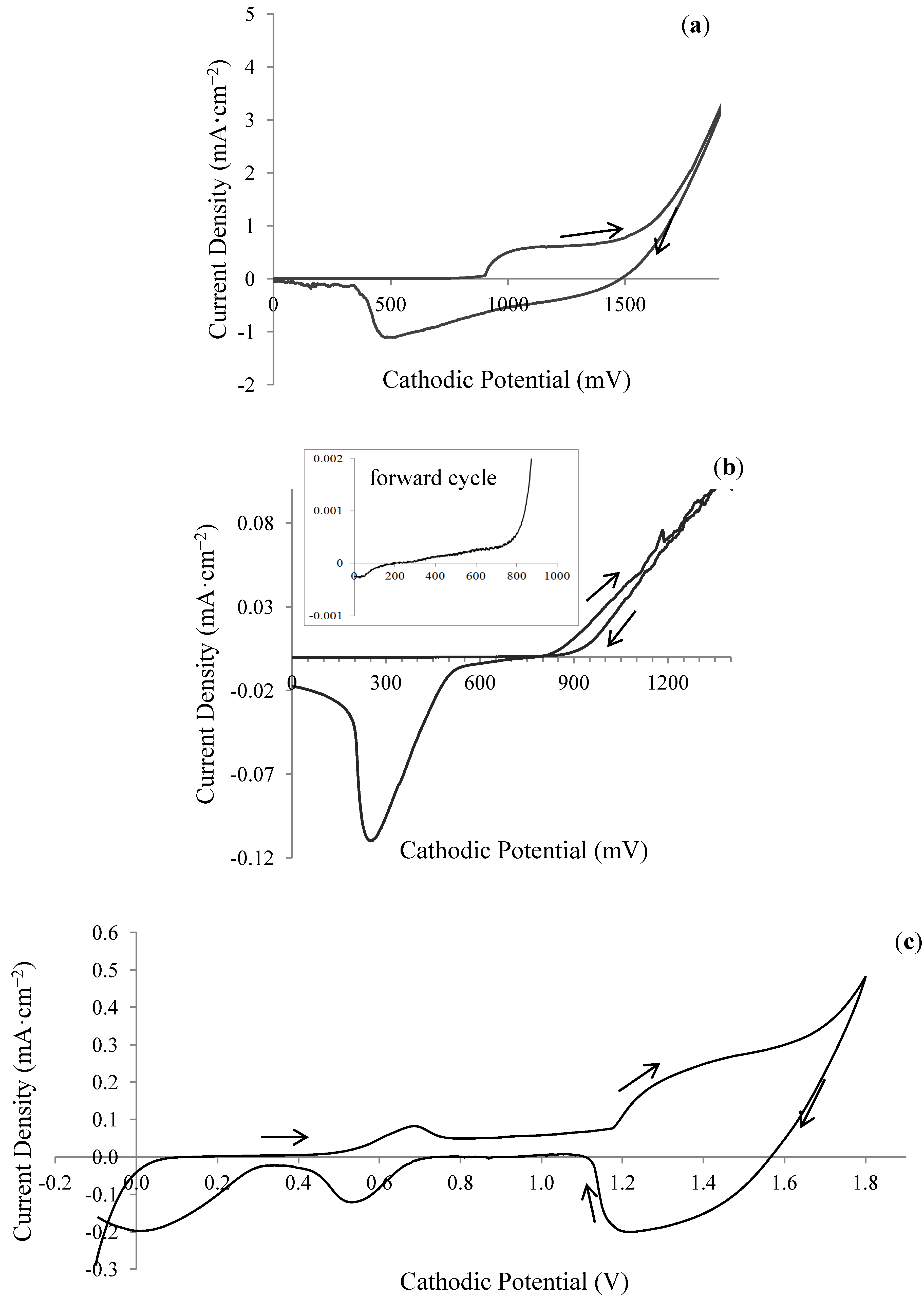
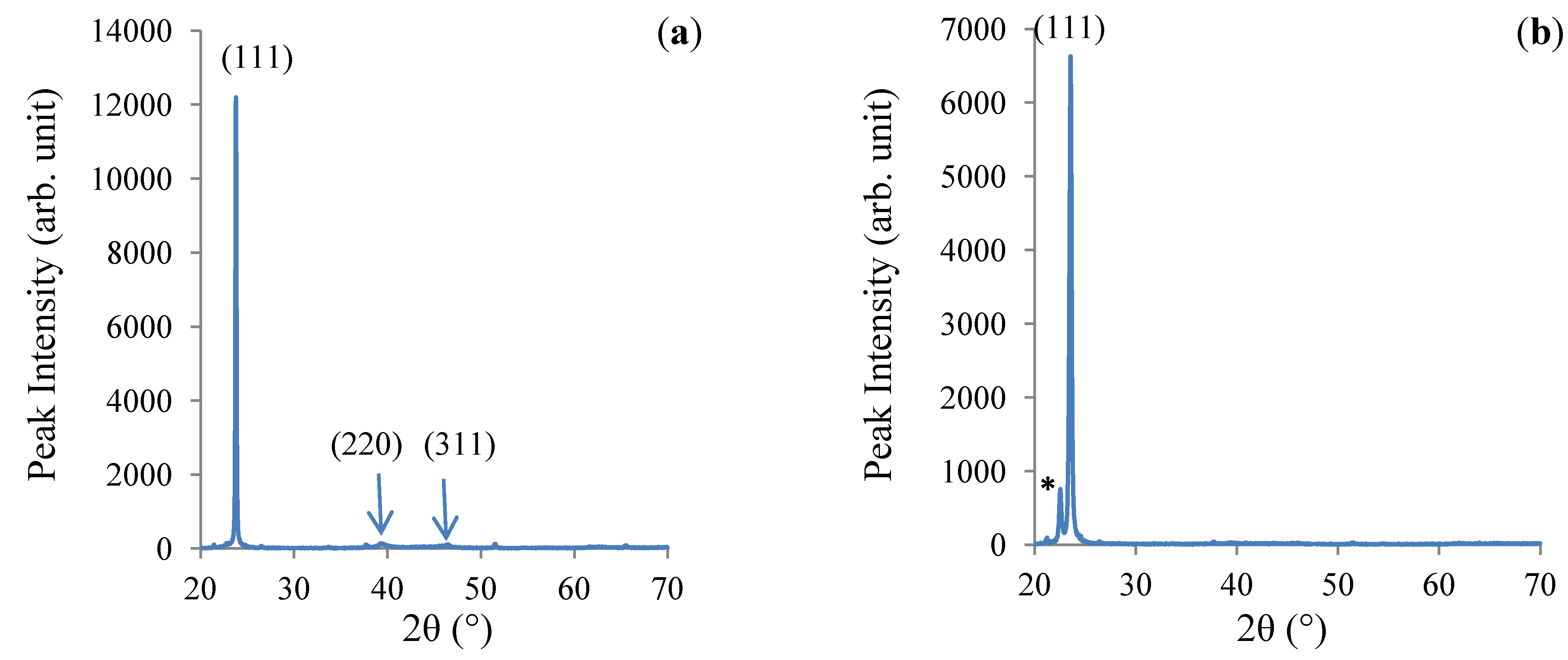
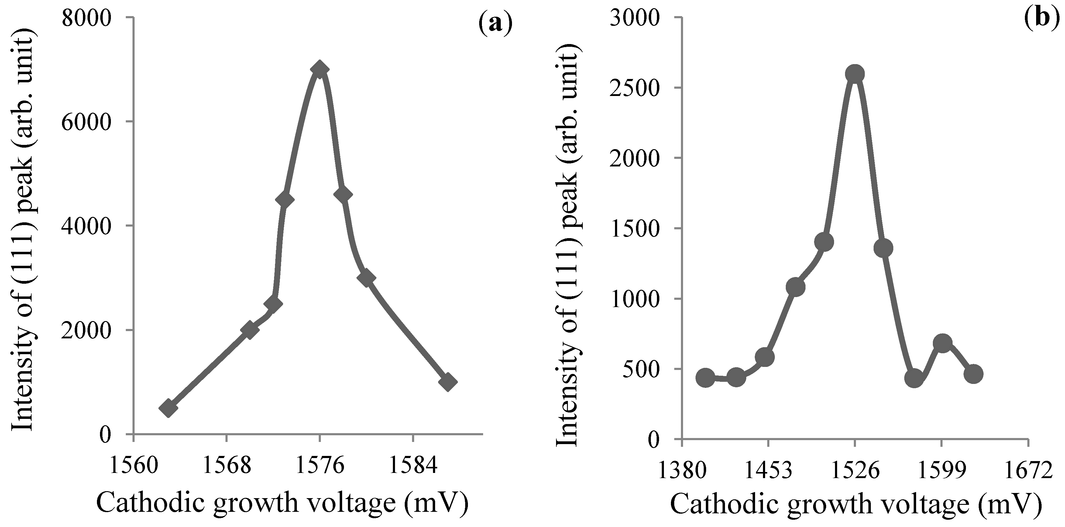
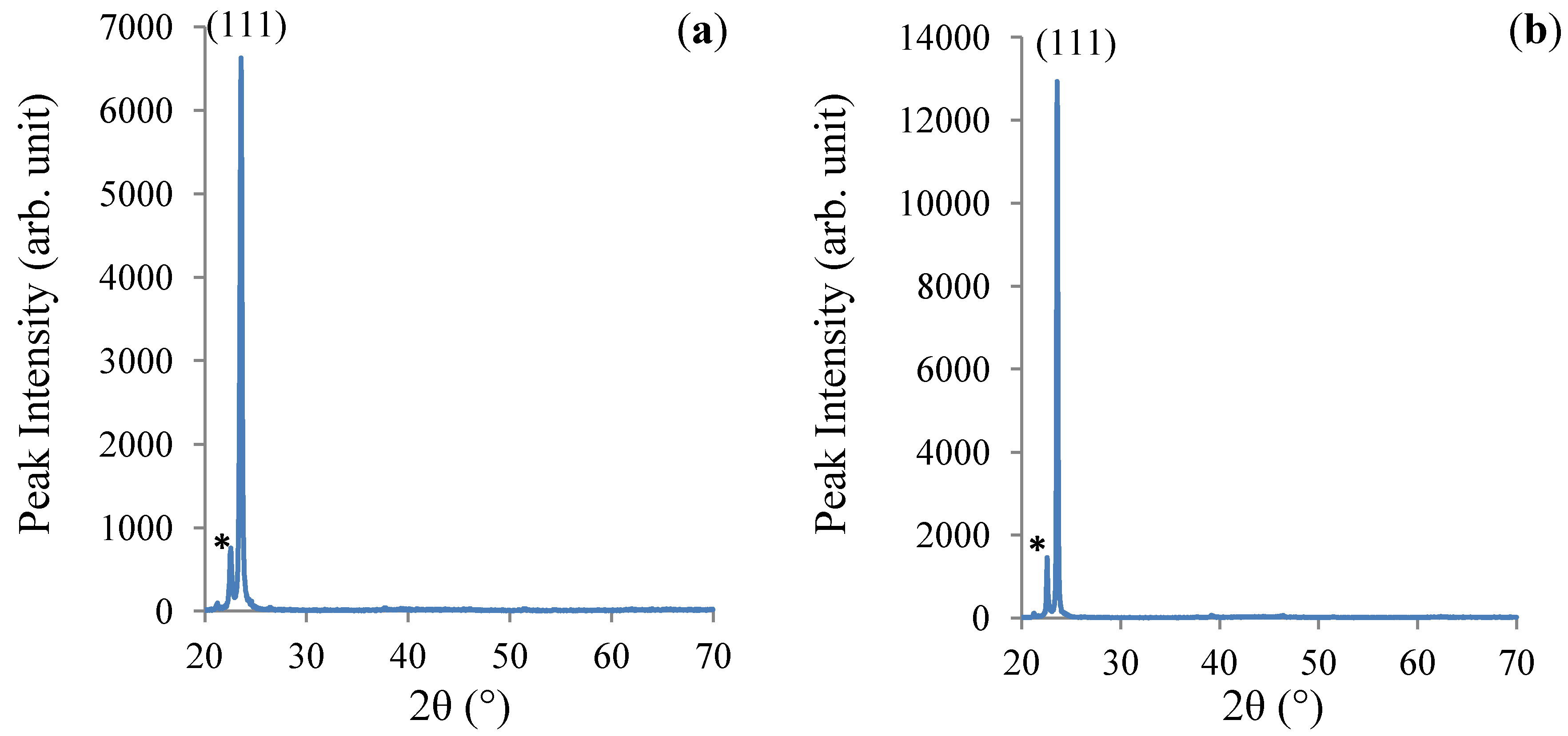
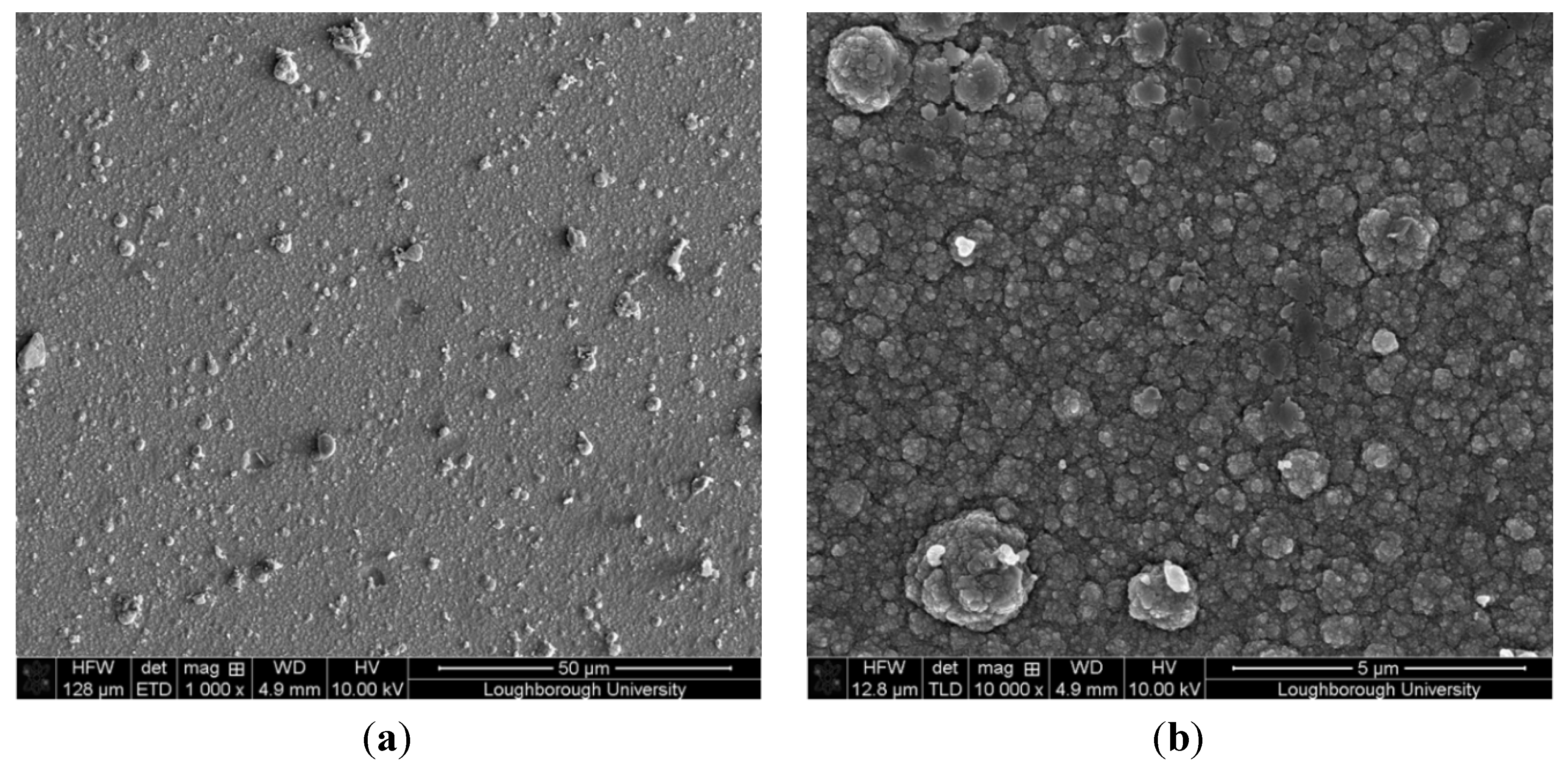
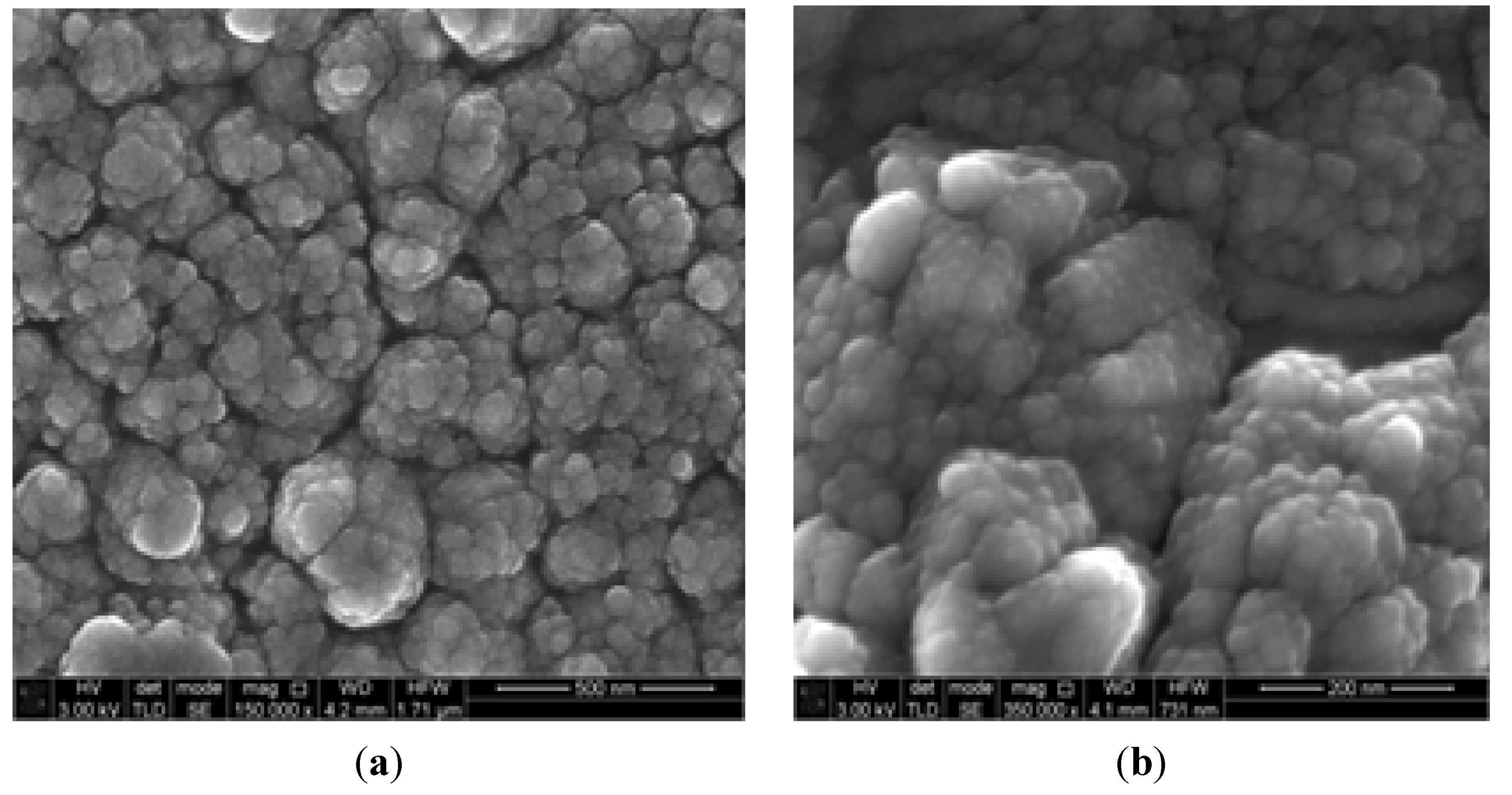
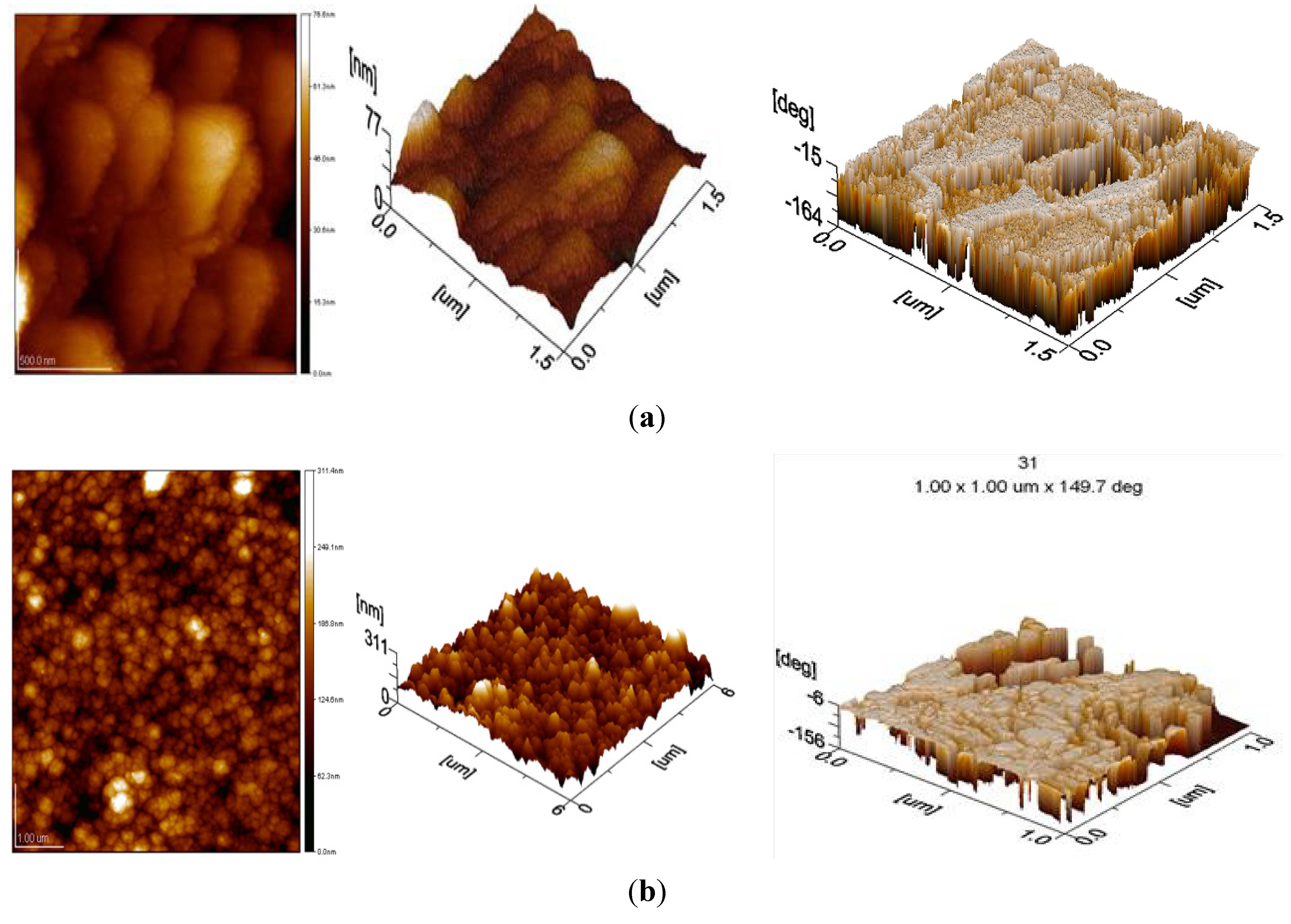
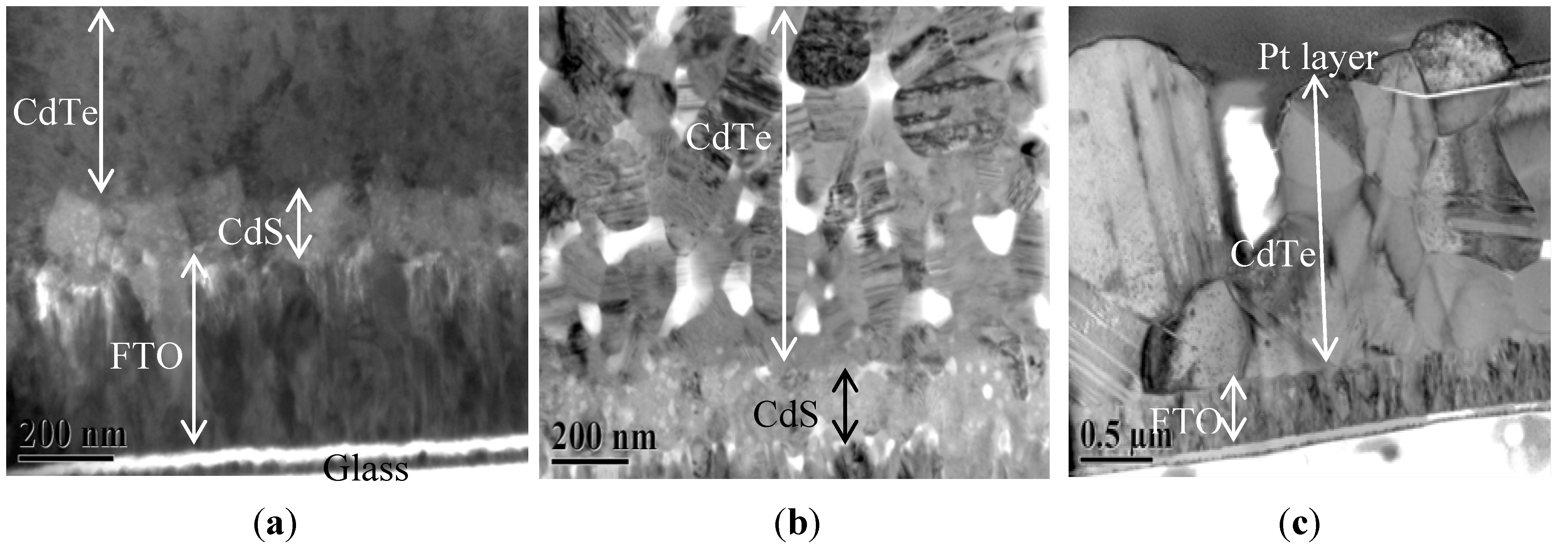
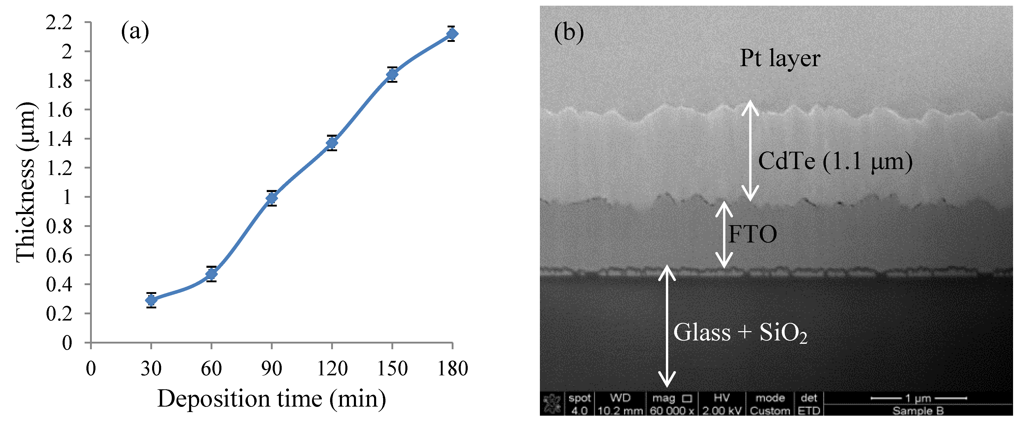
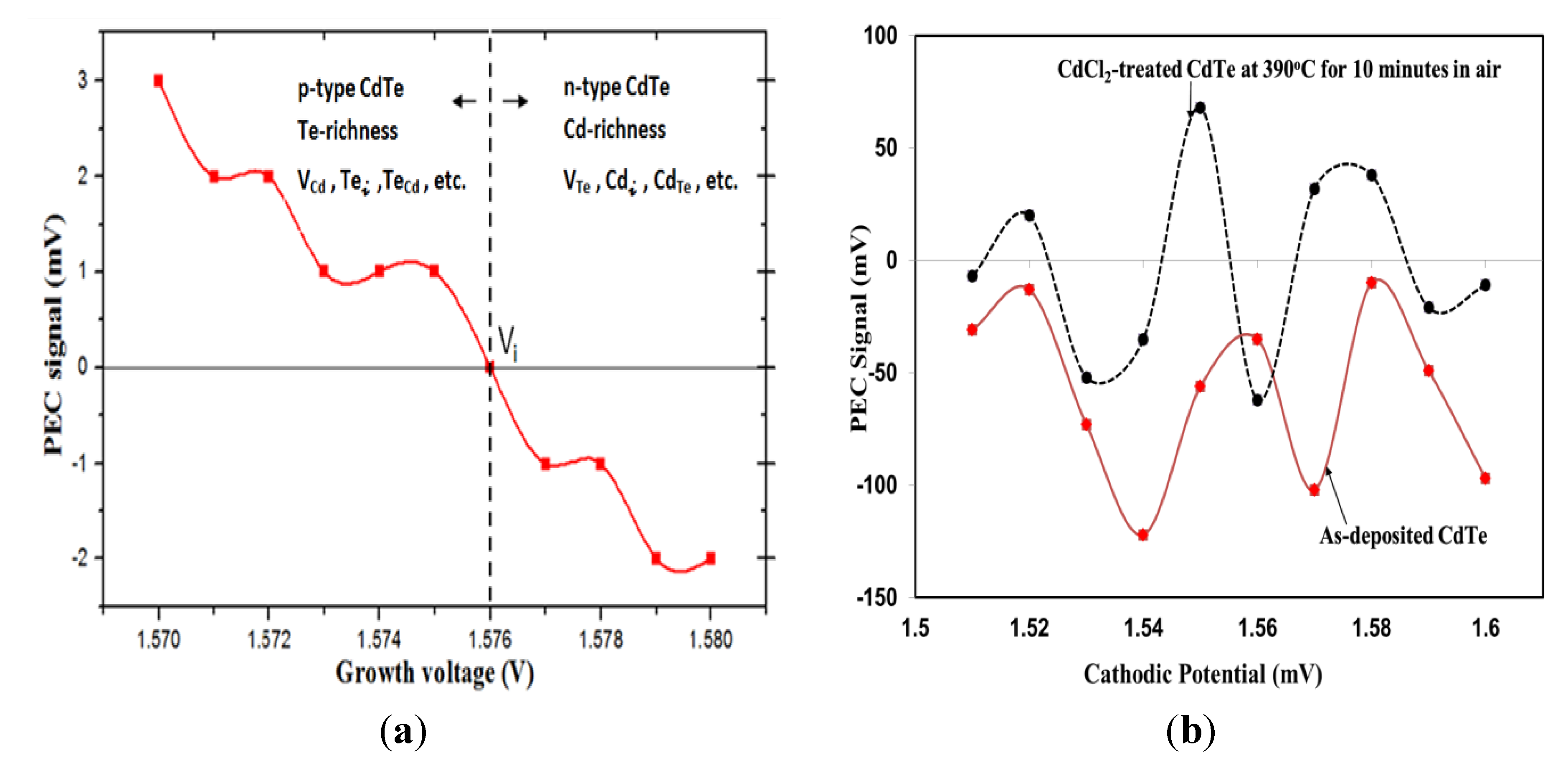
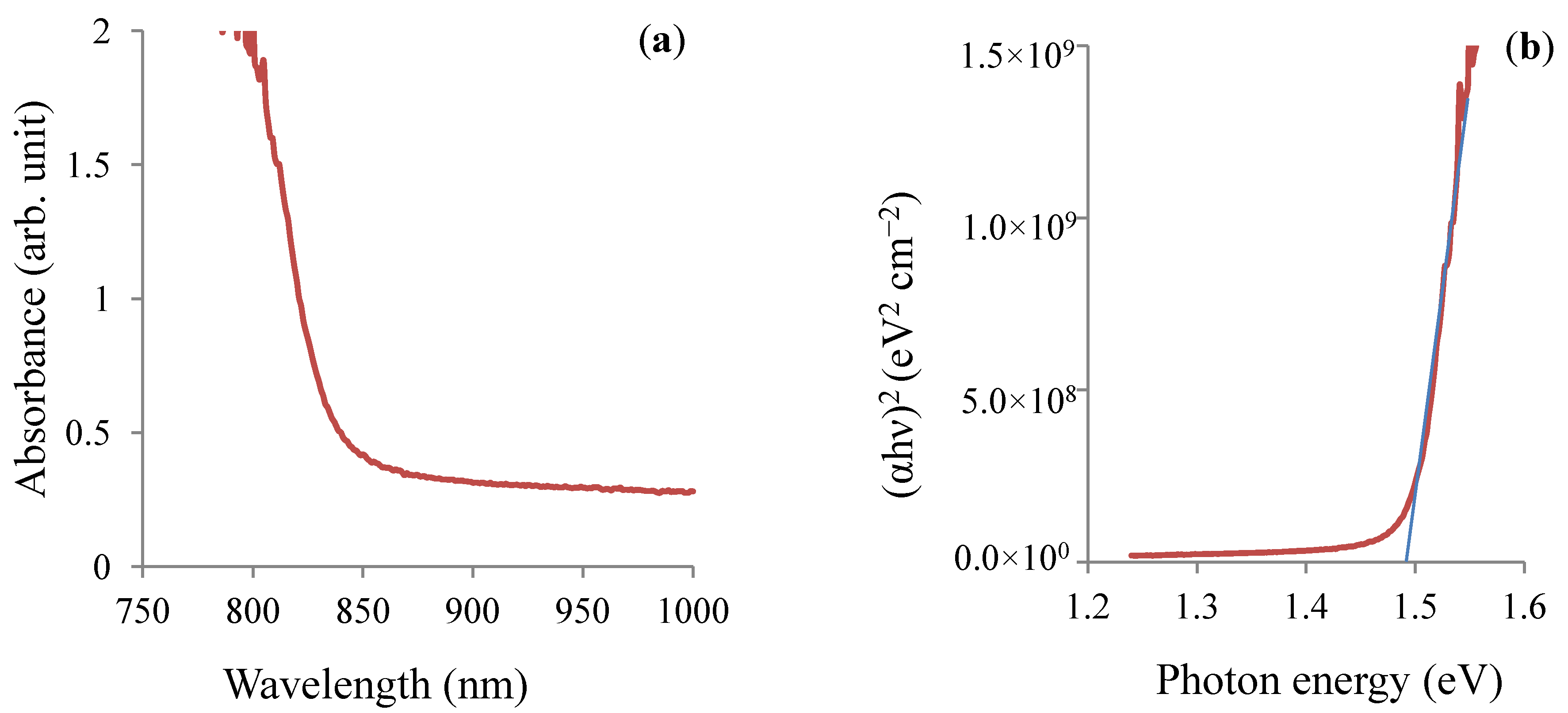
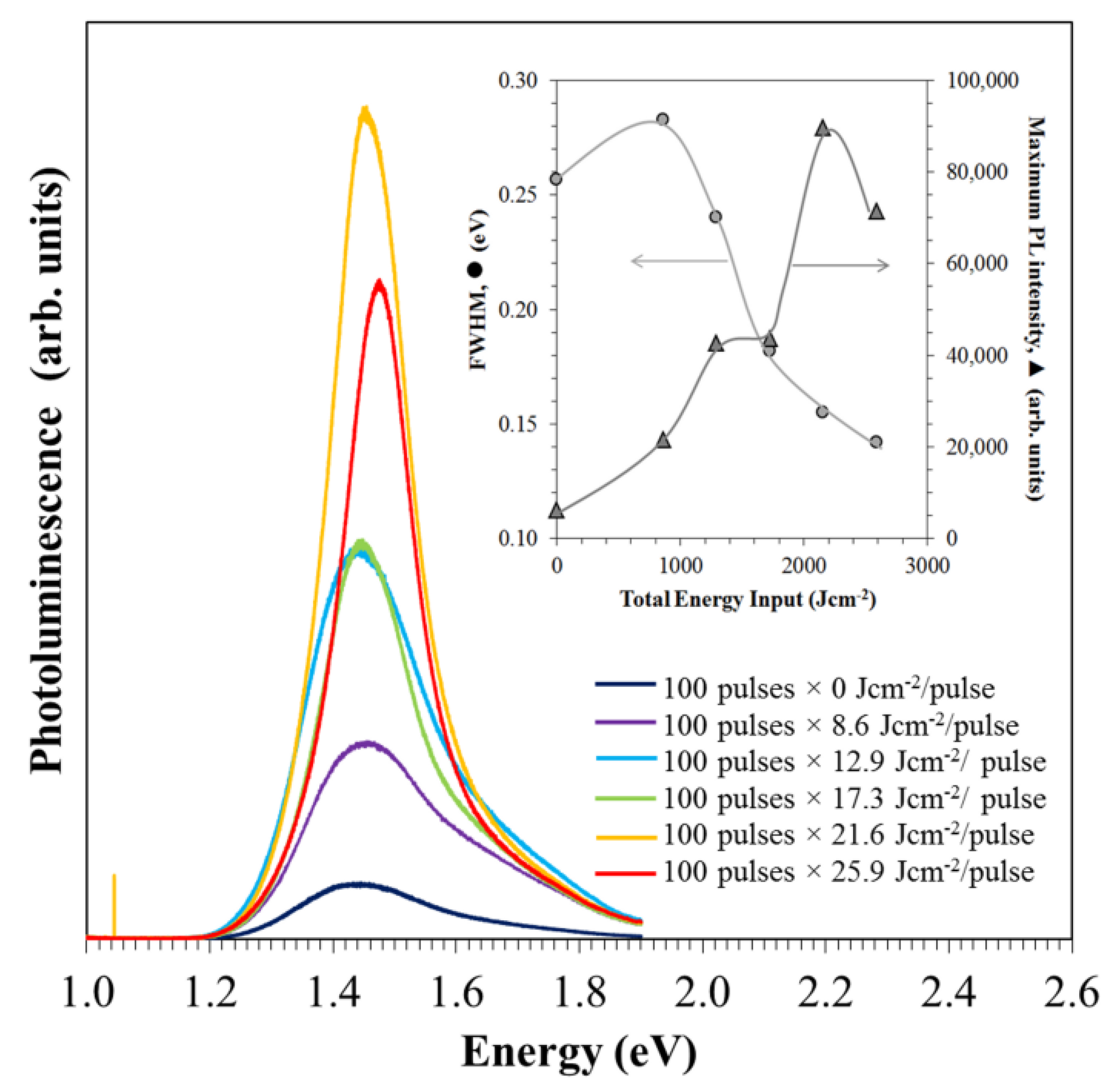
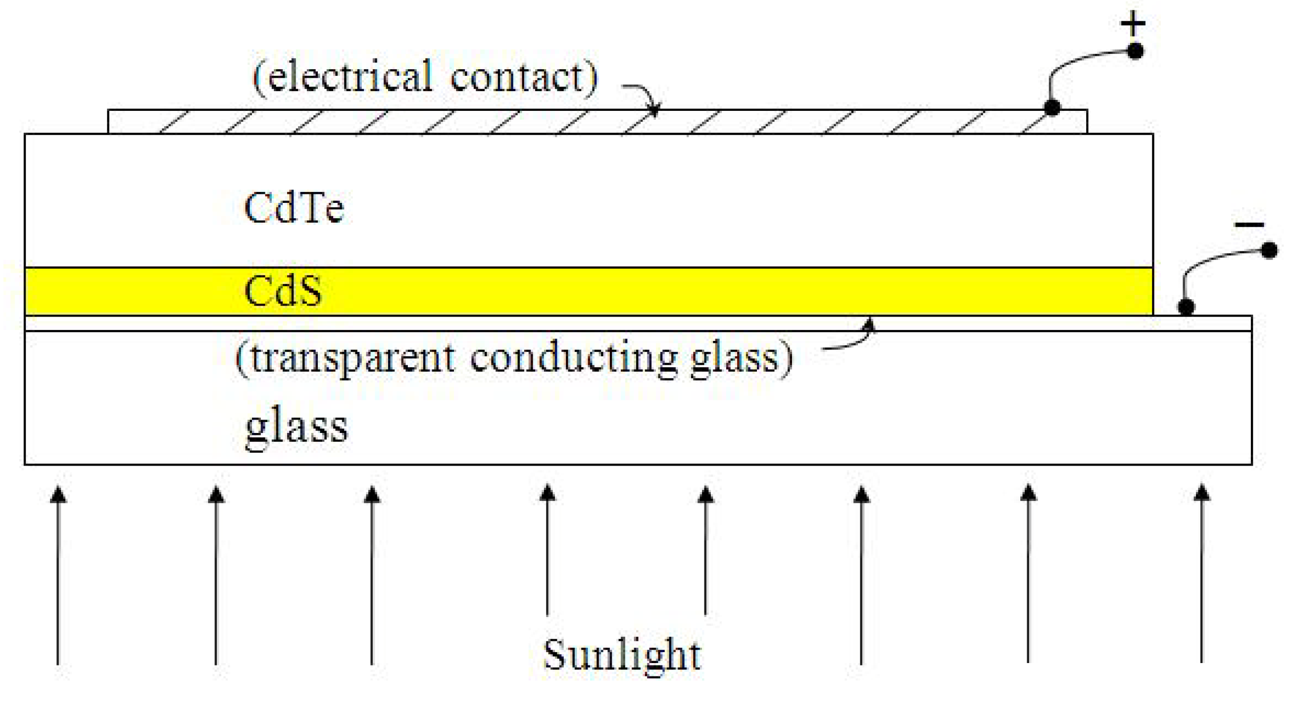
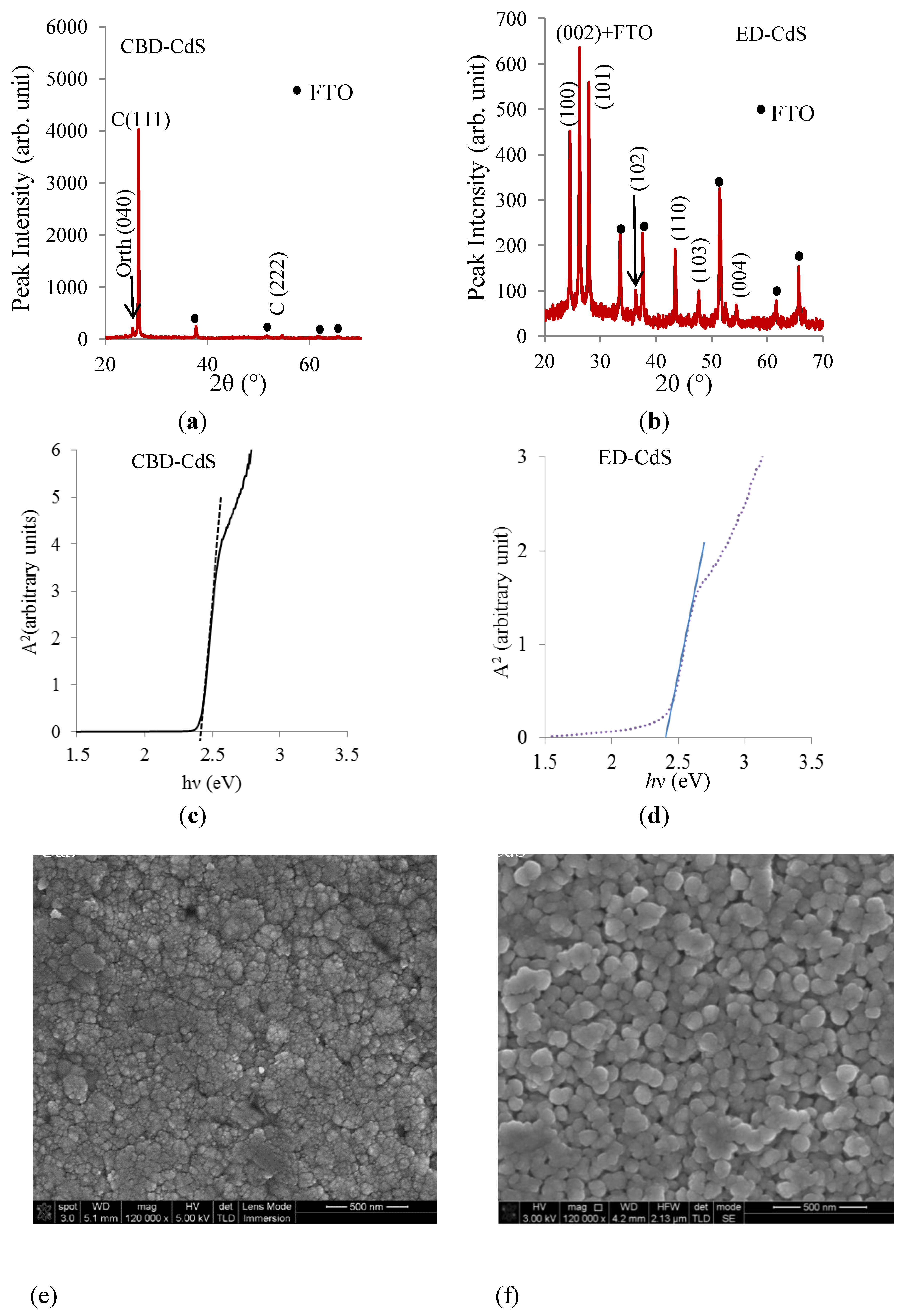
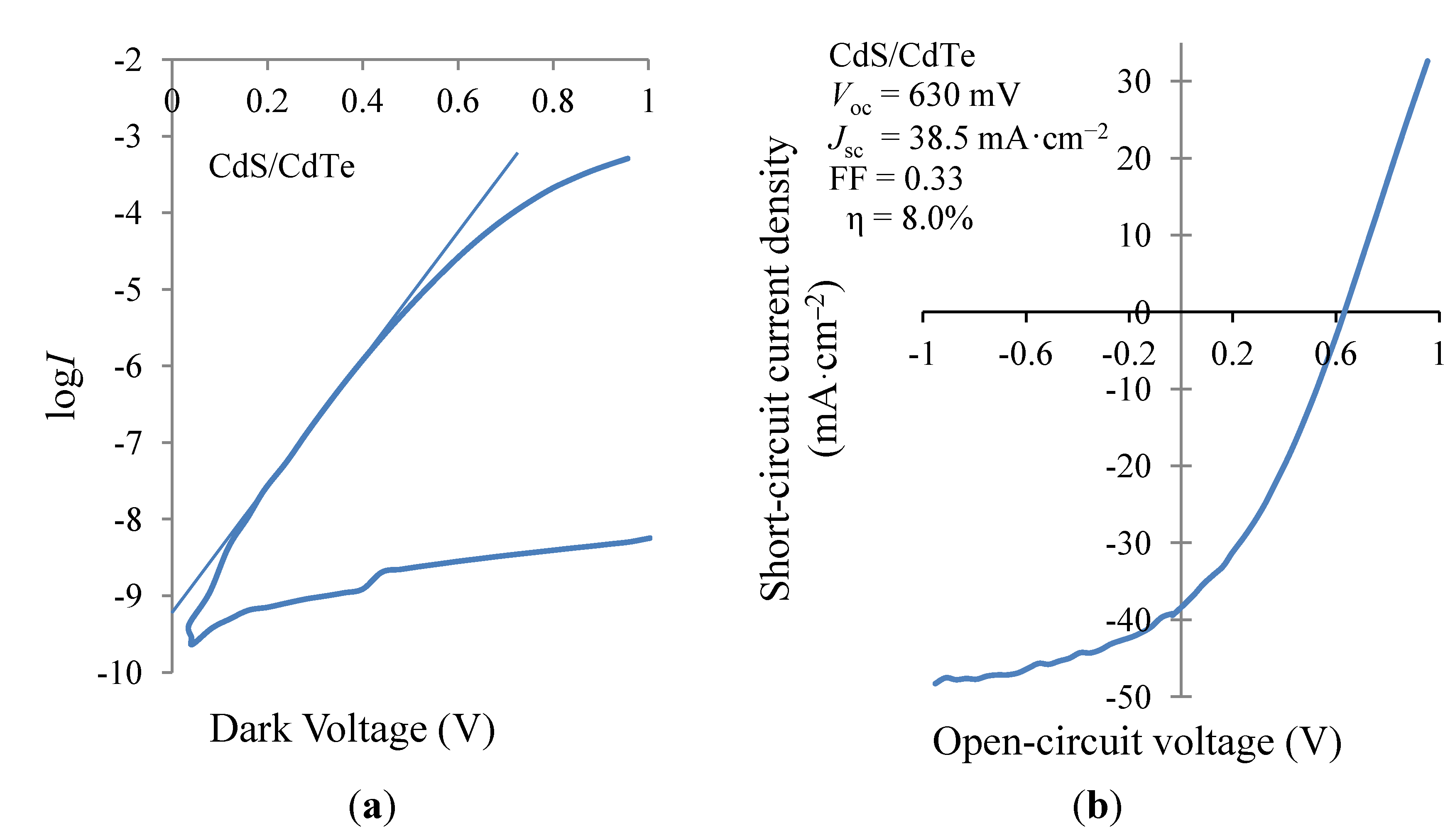
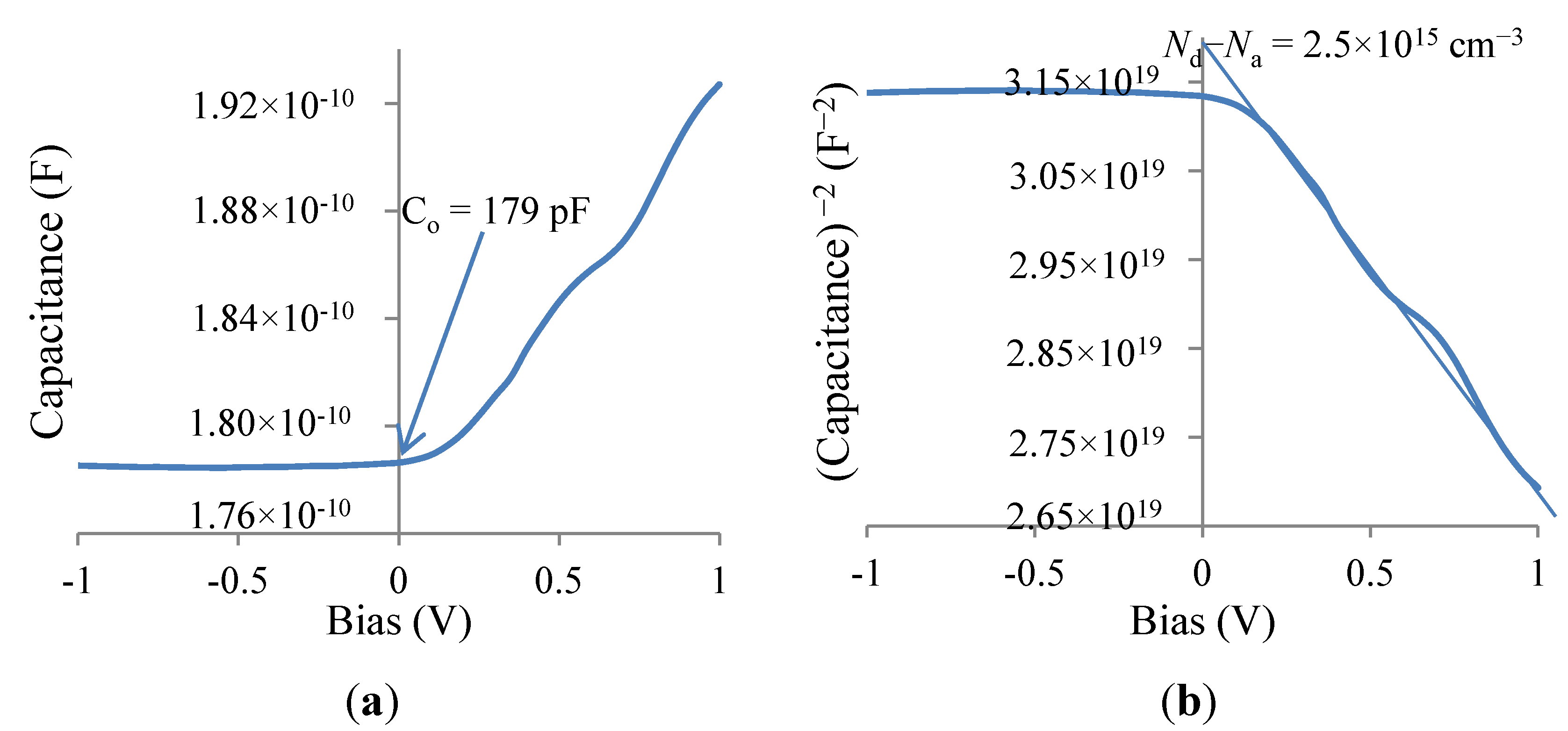
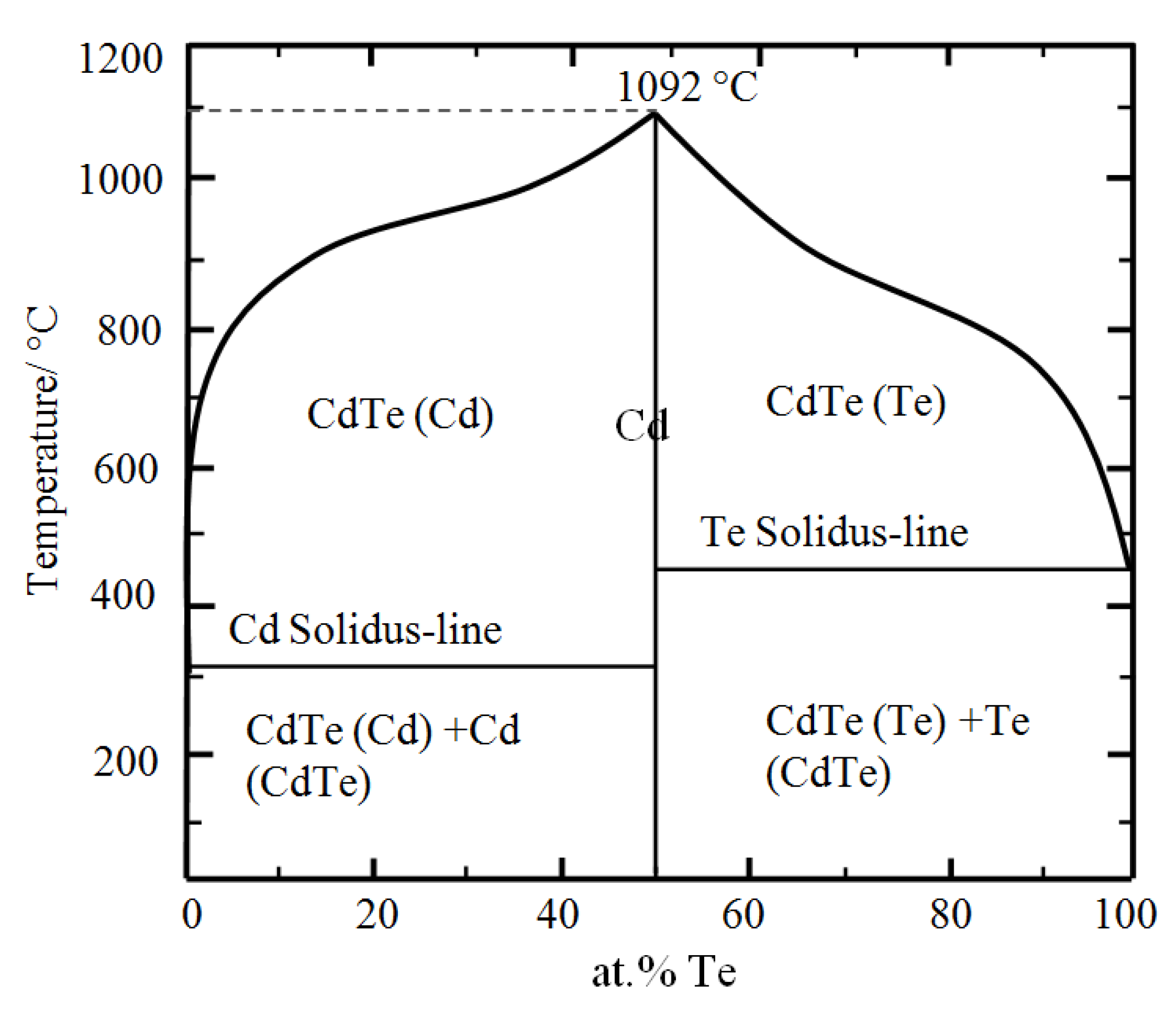
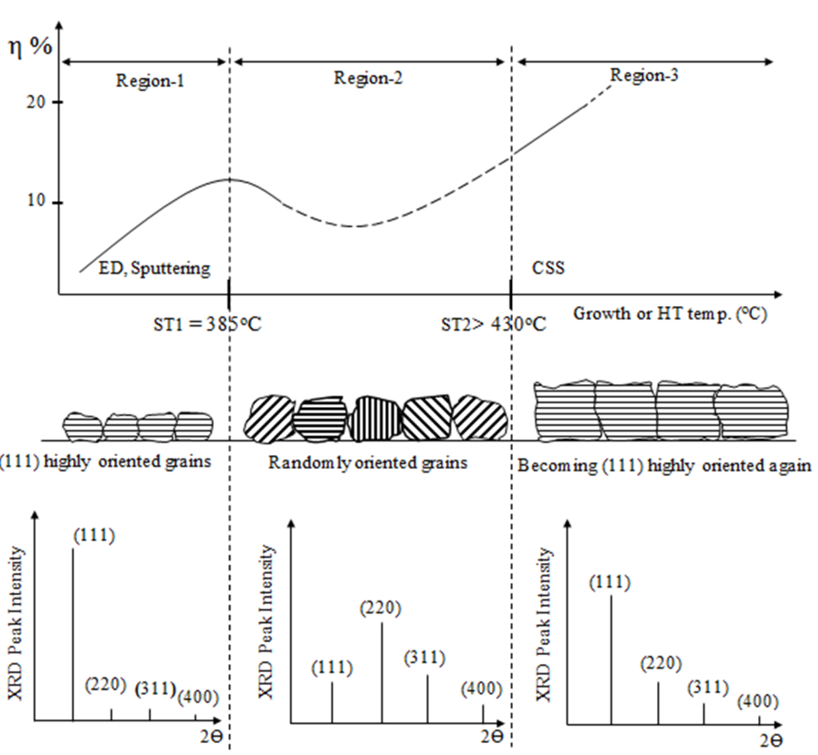
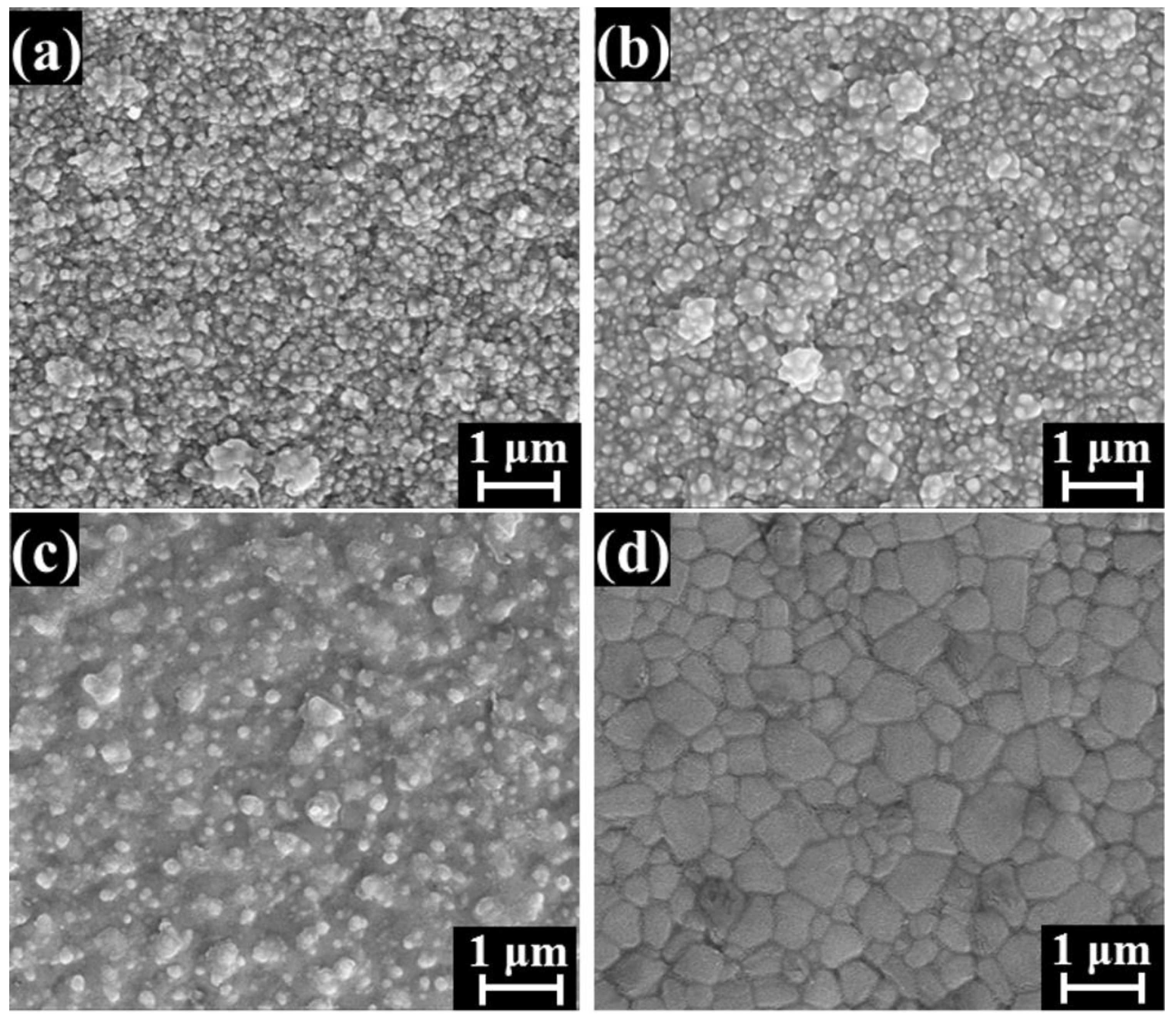
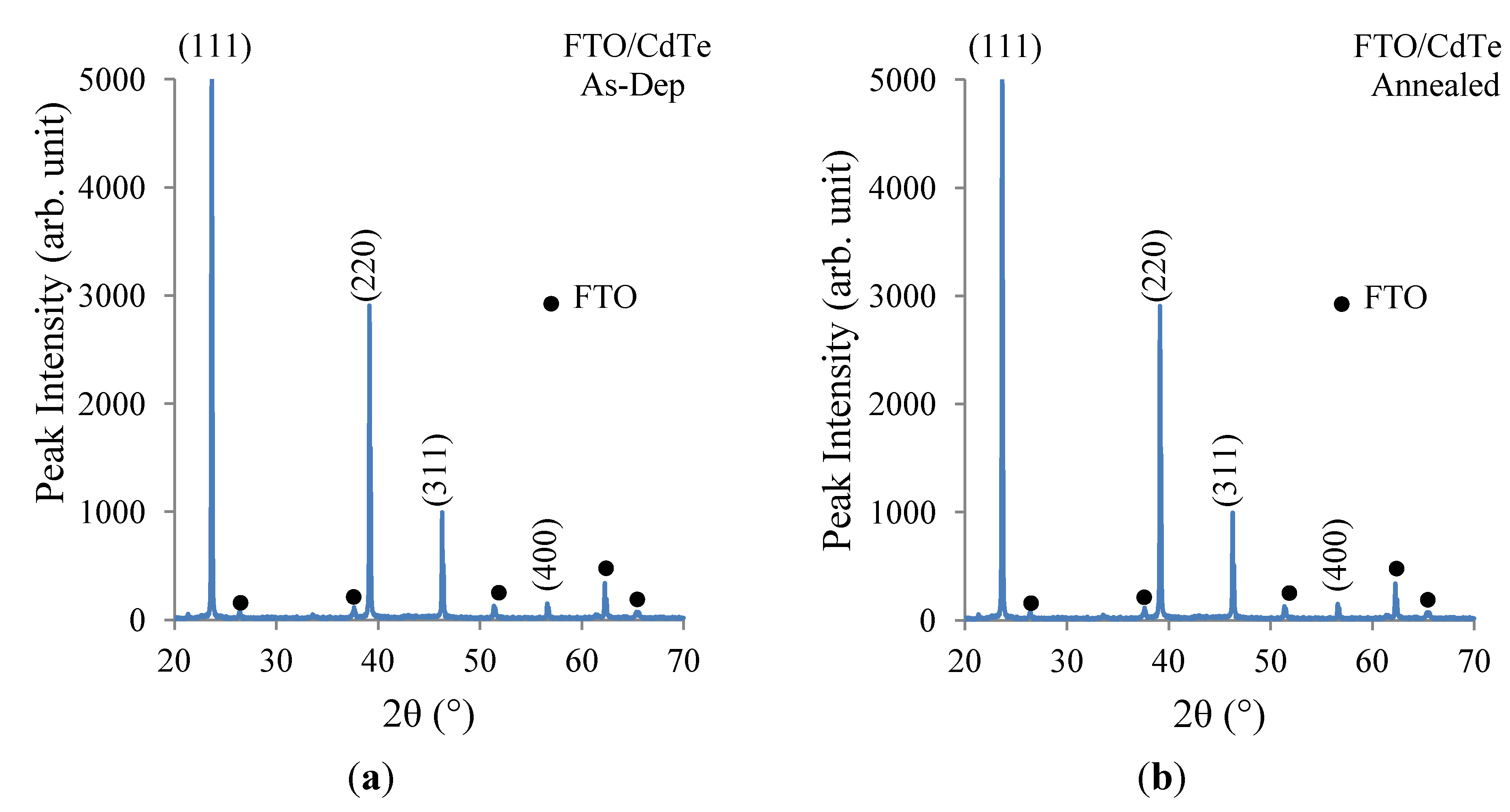
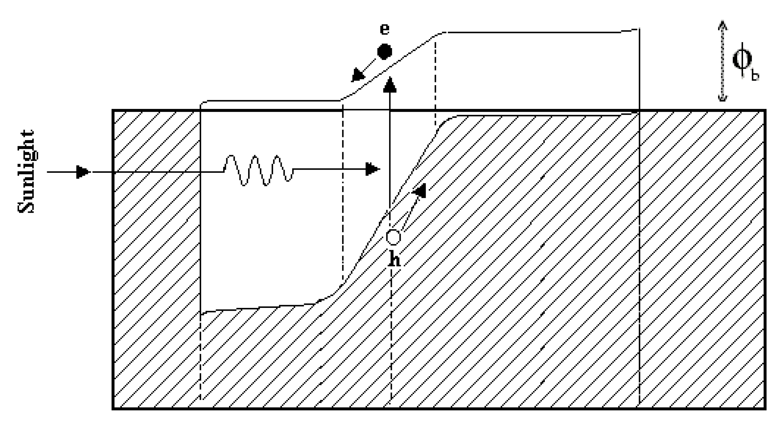
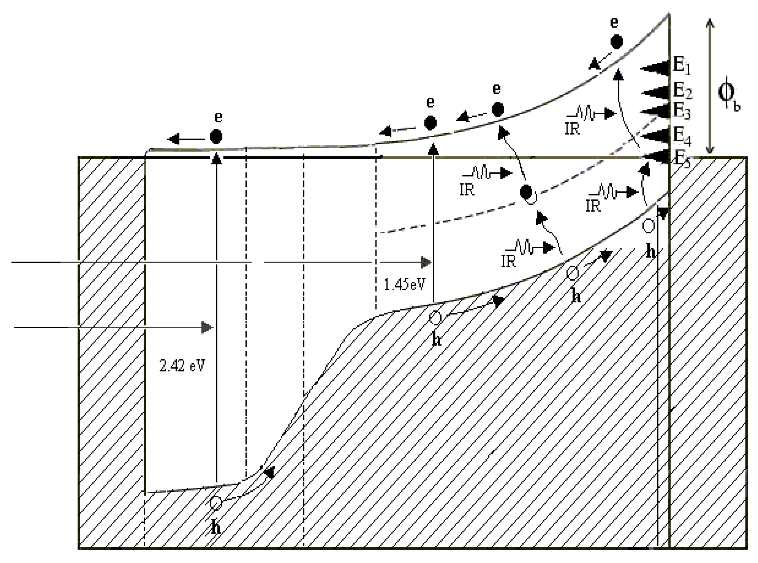
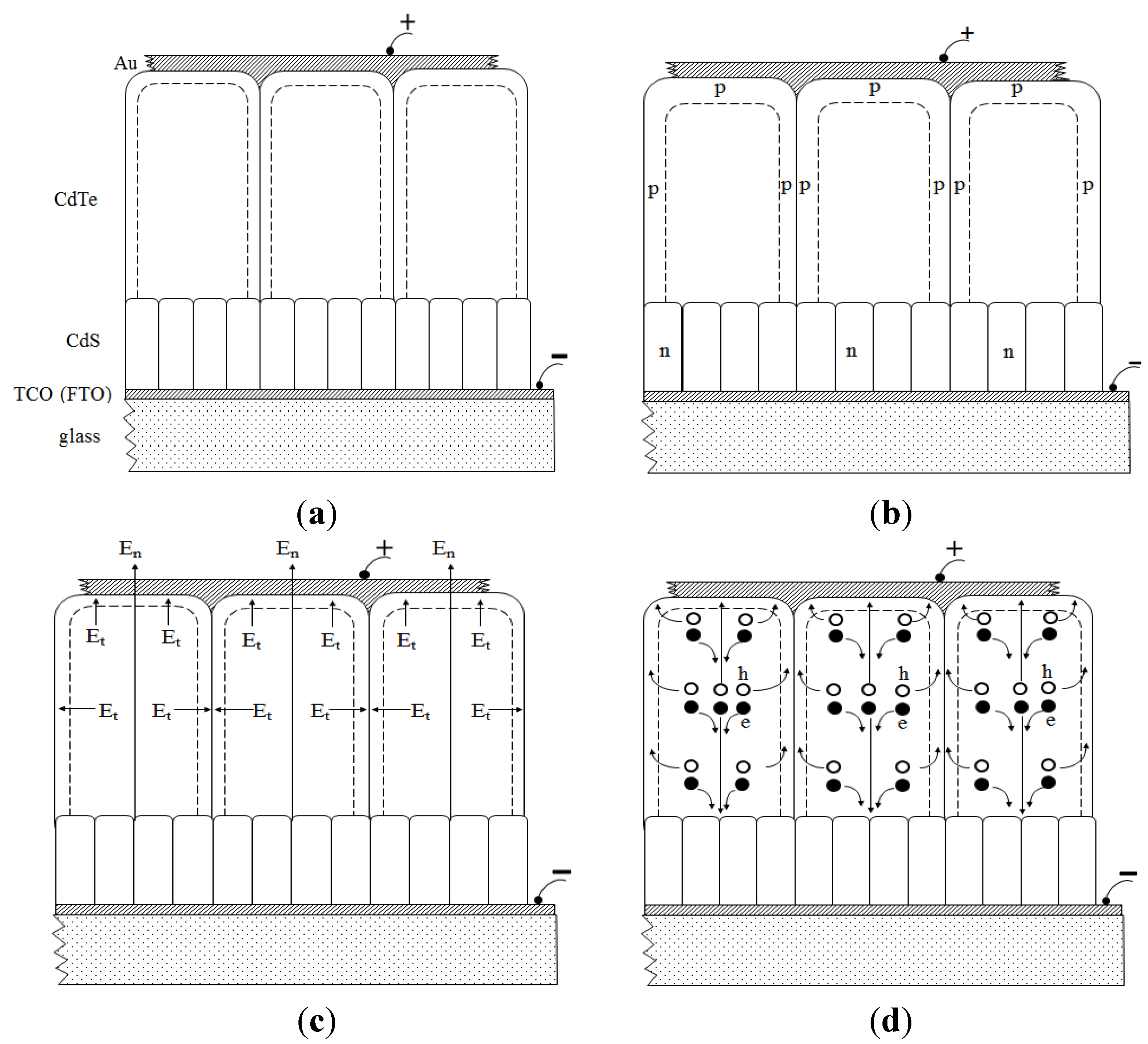
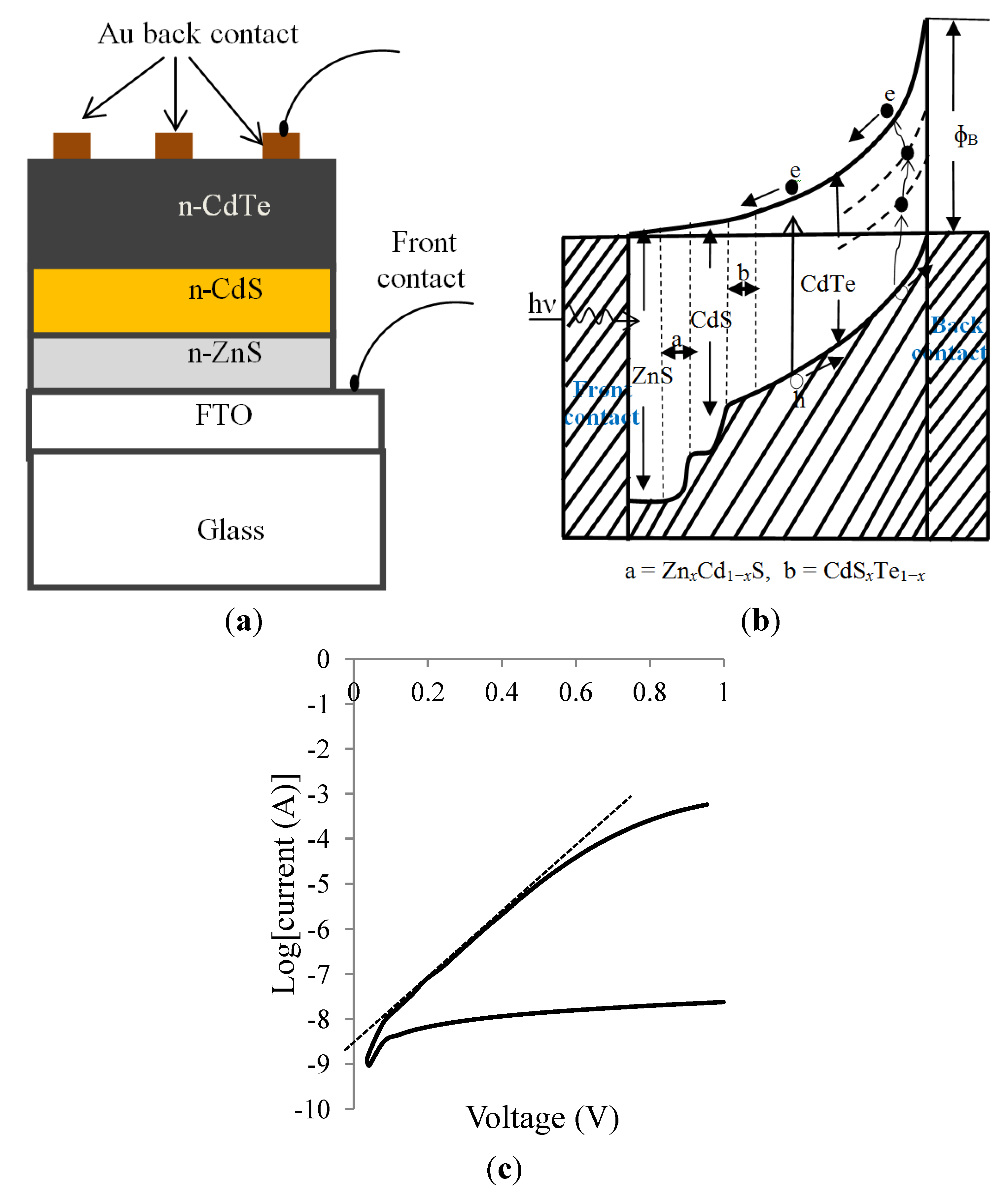


