Article

The Effect of Post-Baking Temperature and Thickness of ZnO Electron Transport Layers for Efficient Planar Heterojunction Organometal-Trihalide Perovskite Solar Cells

1
Department of Chemical and Materials Engineering, Chang Gung University, Taoyuan 33302, Taiwan
2
Division of Neonatology, Department of Pediatrics, Chang Gung Memorial Hospital, Linkou, Taoyuan 33305, Taiwan
3
Center for Reliability Sciences and Technologies, Chang Gung University, Taoyuan 33302, Taiwan
4
Department of Engineering and Science, National Tsing Hua University, Hsinchu 30013, Taiwan
5
Electro Organic Division, Central Electrochemical Research Institute, Karaikudi 630 006, Tamil Nadu, India
*
Authors to whom correspondence should be addressed.
Coatings 2017, 7(12), 215; https://doi.org/10.3390/coatings7120215
Submission received: 31 October 2017 / Revised: 10 November 2017 / Accepted: 25 November 2017 / Published: 30 November 2017

Abstract

:
Solution-processed zinc oxide (ZnO)-based planar heterojunction perovskite photovoltaic device is reported in this study. The photovoltaic device benefits from the ZnO film as a high-conductivity and high-transparent electron transport layer. The optimal electron transport layer thickness and post-baking temperature for ZnO are systematically studied by scanning electron microscopy, photoluminescence and time-resolved photoluminescence spectroscopy, and X-ray diffraction. Optimized perovskite solar cells (PSCs) show an open-circuit voltage, a short-circuit current density, and a fill factor of 1.04 V, 18.71 mA/cm2, and 70.2%, respectively. The highest power conversion efficiency of 13.66% was obtained when the device was prepared with a ZnO electron transport layer with a thickness of ~20 nm and when post-baking at 180 °C for 30 min. Finally, the stability of the highest performance ZnO-based PSCs without encapsulation was investigated in detail.

1. Introduction

Recently, organometal-trihalide perovskite-structured photovoltaic devices (CH3NH3PbX3, X = Cl, Br or I) have received much attention because of their outstanding power conversion efficiency (PCE) and unique optoelectronic characteristics. The characteristics of a high-performance perovskite-structured photovoltaic device include high visible absorption behavior [1], a long carrier diffusion length [2], high ambipolar charge mobility [3,4], tolerance of defect [5], and a simple low-temperature solution process [6]. The first attempt using CH3NH3PbX3 as an active layer for light harvesting was adopted in liquid-type dye-sensitized solar cells with a PCE of 3.8% [7]. The perovskite-structured active layer suffers severe damages from liquid electrolytes because it can be dissolved in polar electrolytes. However, the problem can be improved by using solid hole transport materials to replace the liquid electrolytes [8]. Two main architectures have been used to fabricate perovskite solar cells (PSCs). One is based on a mesoporous TiO2 scaffold, a perovskite-structured active layer, a hole transport layer (2,2′,7,7′-Tetrakis-(N,N-di-4-methoxyphenylamino)-9,9′-spirobifluorene,spiro-MeOTAD), and an Au electrode, which has achieved a power conversion efficiency as high as 22.1% [9]. The other consists in planar PSCs and adopts poly(3,4-ethylenedioxtthiophene): polystyrene sulfonic acid (PEDOT:PSS) and [6,6]-phenyl-C61-butyric acid methyl ester (PCBM) as hole and electron transport materials, respectively. Since the PEDOT:PSS and PCBM are organic materials, the process temperature must be lower than 150 °C. In contrast, the perovskite-structured photovoltaic device with a mesoporous metal oxide scaffold, such as TiO2 or Al2O3, can provide a high specific area substrate on which the perovskite-structured active layer absorber can be grown [3]. As a structure-directing support, the TiO2 scaffolds need to accept the electrons from the absorber and transport them to the electrode. However, TiO2 scaffolds as electron transport layers have certain problems, such as severe J-V hysteresis phenomena owing to poor conductivity of TiO2 [10]. While TiO2 presents a single anatase phase, the electron transport properties can be improved by ascending the calcination temperature to 500 °C [11]. However, the disadvantage of TiO2 is that high-temperature sintering is often required to obtain the desired nanostructures, which is a barrier to low cost and stretchable device fabrication. ZnO is a practical alternative to TiO2 to the electron transport layer of solar cells [12,13], lasing [14], detectors [14], LED [15], etc. since it is also an n-type material with a wide direct band gap (Eg = 3.37 eV at 300 K). The low-temperature process ability, comparable energy levels, and ambient stability make it an excellent electron transport material [16]. Furthermore, ZnO shows an electron mobility higher than that of TiO2, which makes it a potential candidate for electron transport layers. Moreover, the ZnO electron transport layer can be easily deposited through electrodeposition [17], atomic layer deposition [18,19,20], or spin-coating [21,22,23]. These methods are carried out without the need for a high-temperature sintering step, so it is an ideal material for deposition onto thermally sensitive substrates, such as ITO glass or ITO/PET substrates.
Timothy et al. [24] and Song et al. [22] reported low-temperature ZnO nanoparticle processing. Zhang et al. [25] employed low-overvoltage electrodeposition on ZnO layers with PSCs. Seok et al. [26] implemented highly dispersed Zn2SnO4 nanoparticles as an electron transport layer in a perovskite photovoltaic device at a low temperature. Despite being promising for low-temperature processing, these steps comprise time-consuming precipitation, dilution, and washing processes coupled with long reaction times, a need for sophisticated handling, and/or delicate electrochemical machinery [27]. In spite of the several advantages of ZnO, the PCE of ZnO-based PSCs with a traditional n-i-p structure is generally lower than that of TiO2-based PSCs. The problem is that low-temperature processing leaves surface hydroxyl groups and/or residual acetate ligands on the surface of ZnO, and the hydroxyl group decomposes CH3NH3PbI3 into PbI2 and CH3NH3I [28,29]. To avoid this process, the surface of ZnO has been modified by thermal annealing to remove the hydroxide [29], and a buffer layer, such as PCBM and poly(ethylenimine) (PEI), has been placed between the perovskite and ZnO layers to minimize the effect of the surface state of ZnO on the performance of the PSCs [28].
Here, we prepared the ZnO electron transport layer by the simple spin-coating method and then deposited the CH3NH3PbI3 layer in a two-step process [1]. The influences of the thickness and baking temperature of the ZnO electron transport layer on the performance and stability of the solar cells were investigated systematically. The surface morphology, crystallization, and defects of the ZnO films were evaluated via scanning electron microscopy (SEM), X-ray diffraction (XRD), photoluminescence and time-resolved photoluminescence spectroscopy (TRPL), and atomic force microscopy (AFM). The effect of ZnO electron transport layers on the performance of perovskite photovoltaic devices was revealed. The stability of the performance of the perovskite photovoltaic device was determined over the course of more than 1300 h.

2. Materials and Methods

2.1. Synthesis of ZnO Precursor

The ZnO precursor solution (0.5 M) was synthesized by mixing 0.910 g of zinc acetate dihydrate (Zn(CH3COO)2), 9.310 g of 2-methoxethanol, and 0.305 g of monoethanolamine (MEA) under stirring at 65 °C for 2 h until a transparent and homogeneous solution was obtained [30].

2.2. Preparation of Perovskite Solar Cells

The fluorine-doped tin oxide (FTO, surface resistivity is ~7 Ω/sq) glass serves as a substrate for this study. It was cleaned by a chemical solution including neutral liquid (Extran® MA 02, Merck, Darmstadt, Germany), acetone, isopropyl alcohol (IPA), and de-ionized water in an ultrasonic bath for 10 min, and dried with a jet of nitrogen. Finally, the substrate was then baked at 100 °C for 30 min to eliminate the residual solvents. Various ZnO electron transport layers were coated on the FTO glass by the spin-coating method at 5000 revolutions per minute (rpm) for 20 s, and baked at different temperatures (100 °C, 120 °C, 150 °C, 180 °C, and 250 °C) for 30 min. After the preparation of the ZnO electron transport layer, the perovskite light harvester was deposited in a two-step process [1]. Lead iodide (PbI2) solution was prepared by dissolving 392.0 mg PbI2 (99.998%, Sigma-Aldrich, St. Louis, MO, USA) in 1.0 mL of N,N-dimethylformamide (DMF, 99.8%, Sigma-Aldrich). The 80.0 μL PbI2 solution was spin-coated on the ZnO electron transport layer at 3000 rpm for 30 s, and baked at 100 °C for 10 min. The 200.0 μL of 0.044 M (7 mg/mL) CH3NH3I dissolved in IPA was spin-coated on the top of the PbI2 layer at 3000 rpm for 30 s, and baked at 100 °C for 10 min to convert it into CH3NH3PbI3 (MAPbI3). The Spiro-MeOTAD in 1.0 mL chlorobenzene was added with 28.8 μL of 4-tert-butyl pyridine (96.0%, Sigma-Aldrich) and 17.5 μL of lithium bis(trifluoromethane sulfonyl) imide (LiTFSI) solution (520 mg/mL acetonitrile (99.8%, Sigma-Aldrich)). One hundred microliters of the Spiro-MeOTAD solution was spin-coated on the MAPbI3 layer at 2000 rpm for 30 s. Finally, the MoO3 layer with a 10 nm thickness and silver electrode with a 100 nm thickness were thermally evaporated on the top of the Spiro-MeOTAD layer, respectively. The construction of the perovskite-structured photovoltaic device is shown in Figure 1a and the energy level of materials in device is shown in Figure 1b.

2.3. Characterization

A scanning electron microscope (S-800, Hitachi, Tokyo, Japan) operated at 10.0 kV was used to produce the SEM images. XRD patterns were collected from 10 to 50° of 2θ with a multi-function high power X-ray diffractometer (D8 Discover SSS, Bruker, Billerica, MA, USA) equipped with a 2D detector using Cu Kα radiation. The solar simulator used was a 3A (AAA) solar simulator (KXL-500F, Wacom, Kazo, Japan). Before each measurement, the intensity of light for the simulator was calibrated by a silicon diode with a KG-5 filter (2.0 cm × 2.0 cm). The silicon diode was calibrated from time to time using a secondary reference silicon cell. The current of the silicon cell with a KG-5 filter under 1.0 sun should be 70.6 mA, which was calibrated by TERTEC Org., Taoyuan, Taiwan (following IEC 60904 [31]). The area of the test cell was 0.10 cm2, which was defined by a thin black metal mask. The computer-controlled digital source meter (Keithley 2400, Keithley, OH, USA) was applied to measure the photocurrent density–voltage (J-V) characteristics under 1.0 sun illumination (100 mW/cm2, AM 1.5G). AFM (Dimension-3100 Multimode, Veeco Digital Instruments, Plainview, NY, USA) in tapping mode was used to measure the surface morphology of various ZnO electron transport layers. The steady-state PL spectra were recorded by pumping the specimen with different ZnO electron transport layers using a continuous-wave diode laser (λexe ~ 440 nm, PDLH-440-25, Dong Woo Optron Co. Ltd., Seoul, Korea). The recorded data were analyzed by a photomultiplier tube detector system (PDS-1, Dong Woo Optron Co. Ltd.) and a monochromator (Monora150i, Dong Woo Optron Co. Ltd.) of standard photon-counting electronics. TRPL spectra were measured by a time-correlated single photon counting (WELLS-001FX, Dong Woo Optron Co. Ltd.) spectrometer. A pulse laser (λexe ~ 440 nm) with an average power of 1.0 mW, operating at 312.5 MHz, with a 2 μs duration was used for excitation.

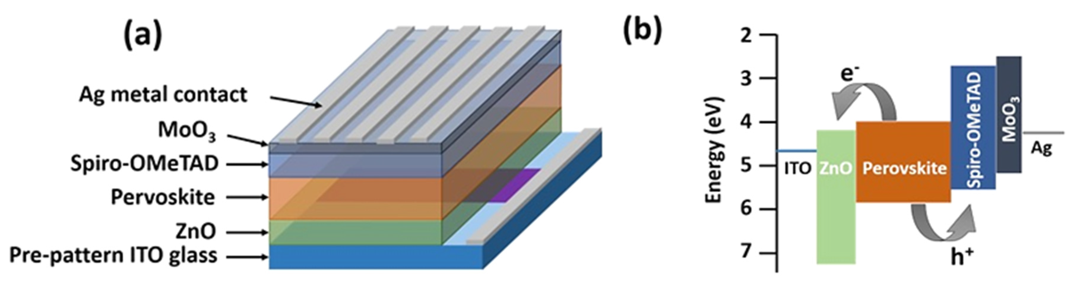
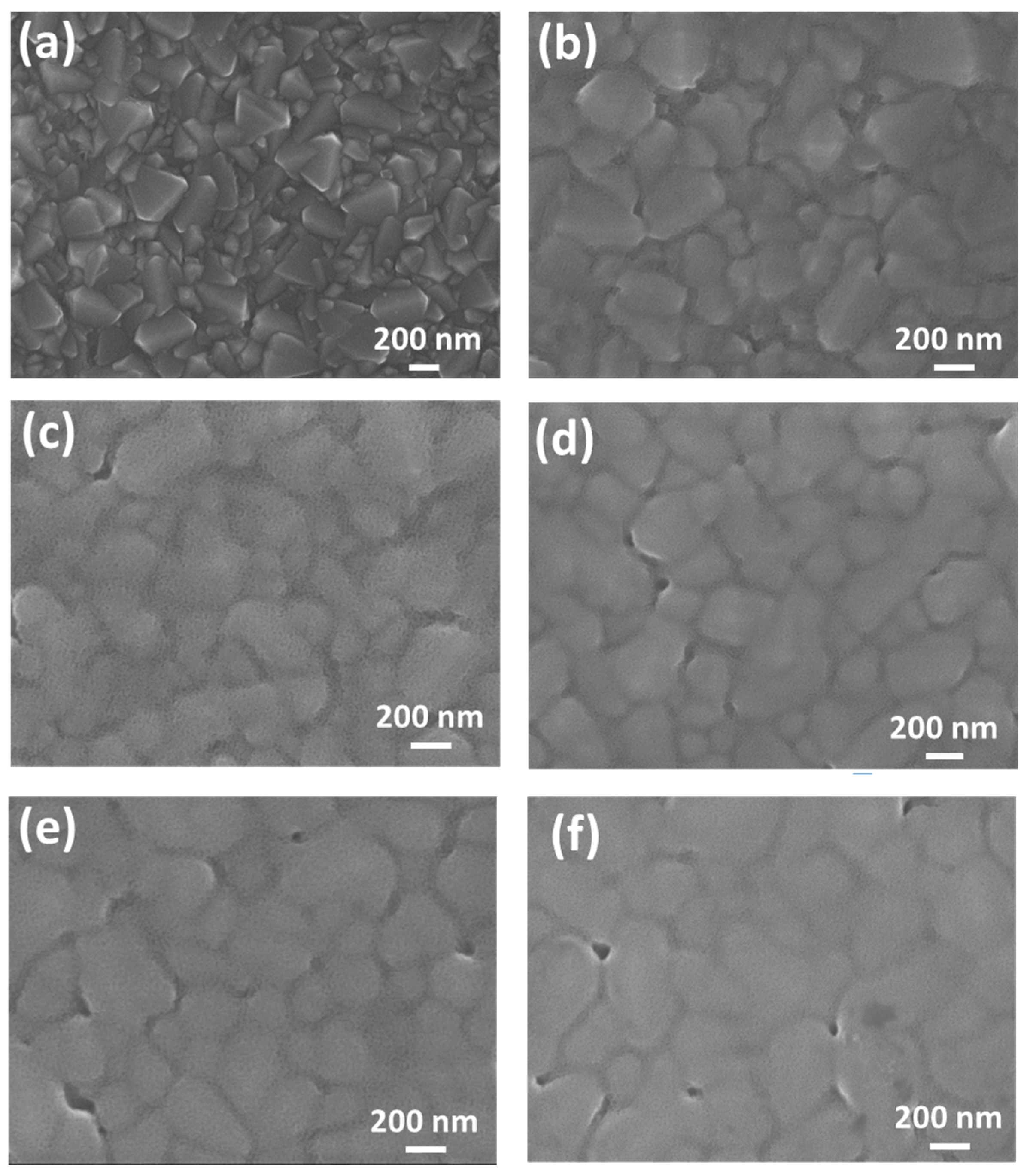
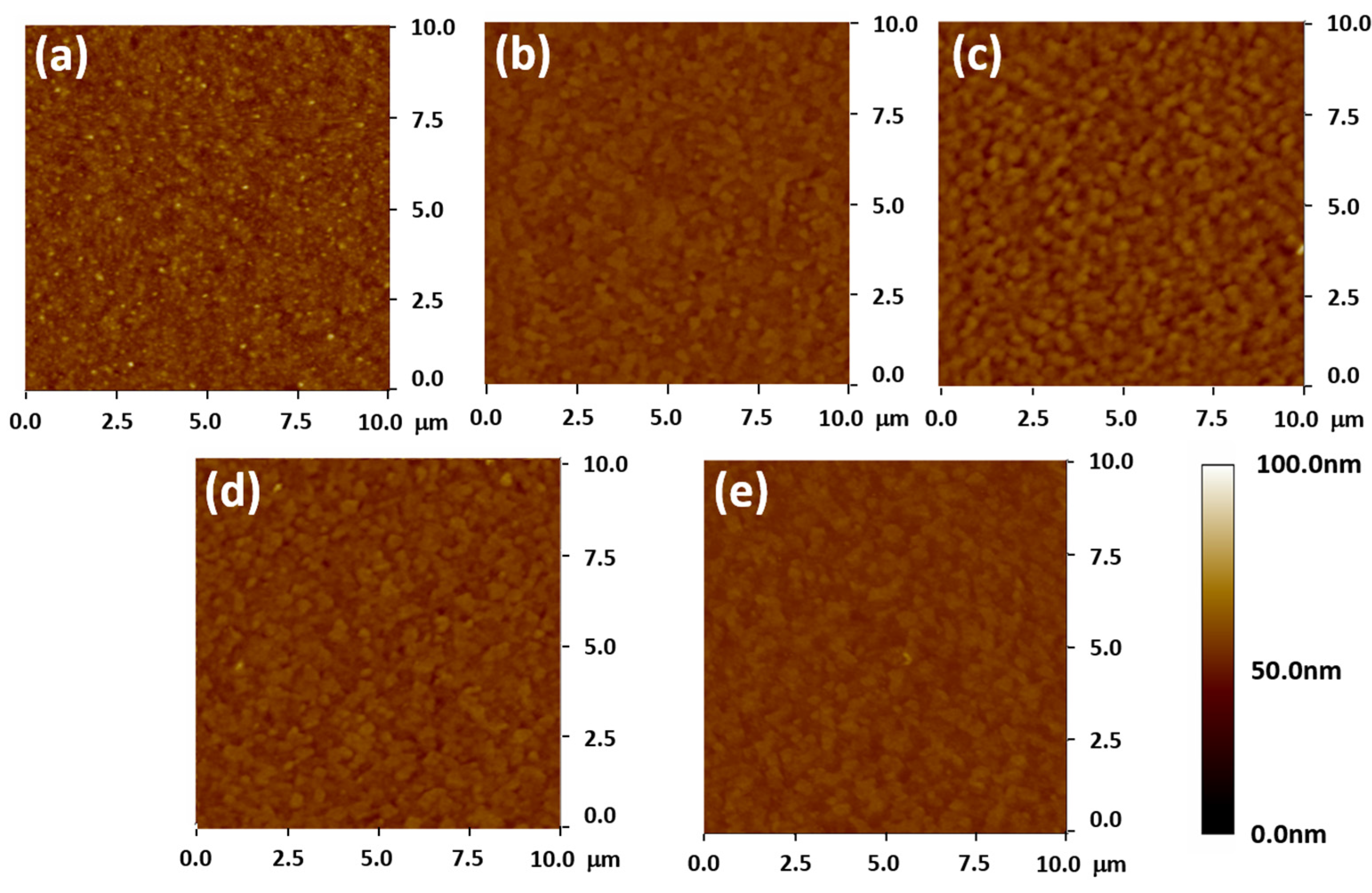
3. Results and Discussion

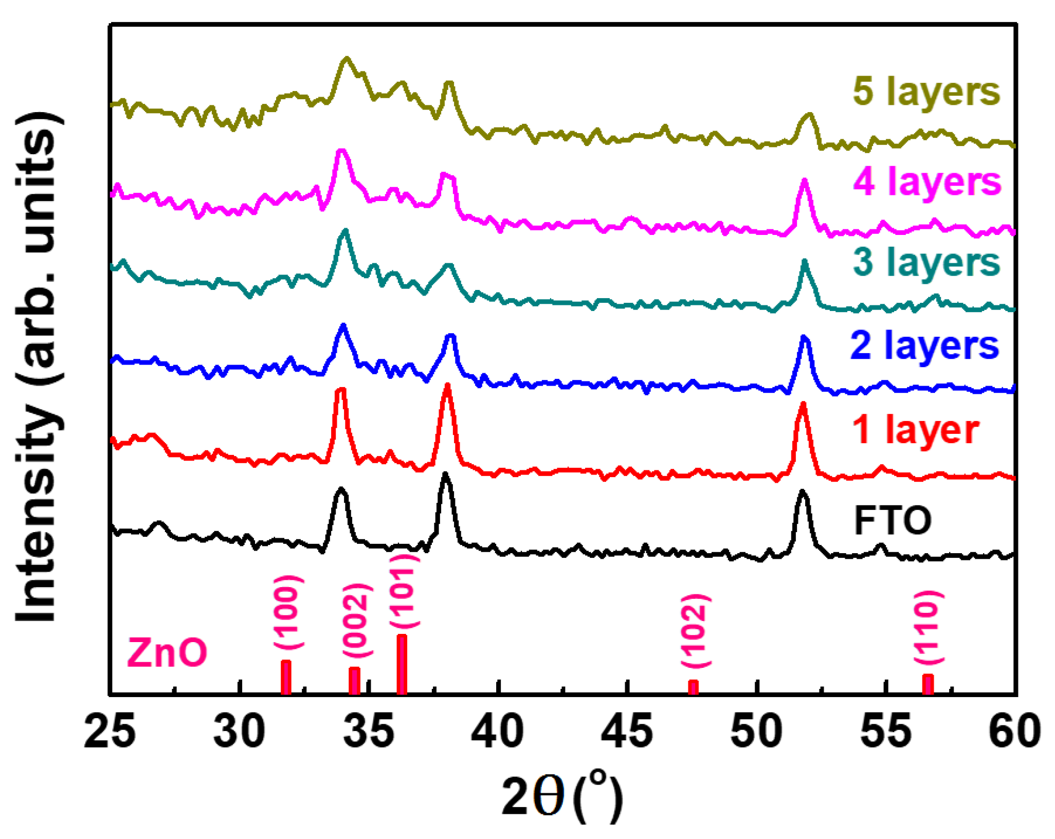
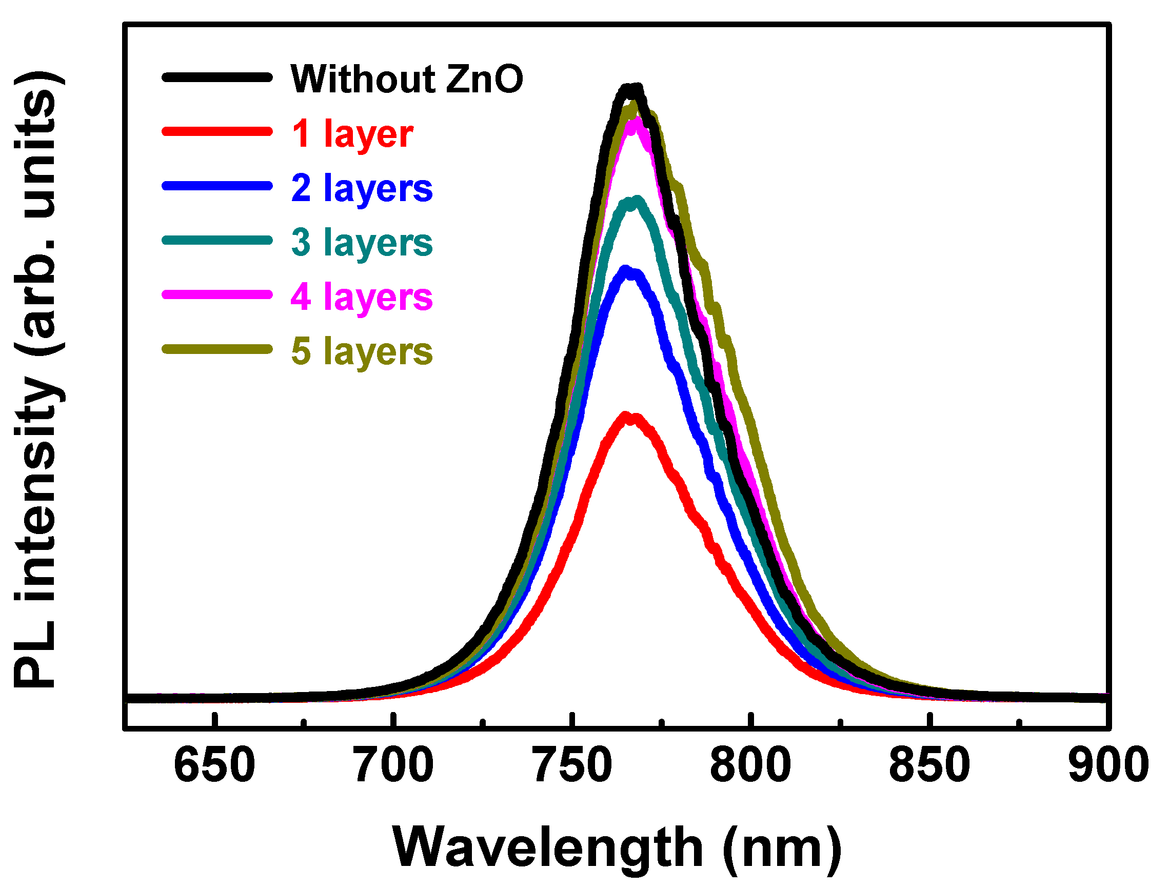
3.1. Influence of ZnO Electron Transport Layer Thickness

The construction of the PSC and an energy level diagram is shown in Figure 1. Figure 2 shows the surface microstructure of various ZnO electron transport layers with different coating layers. It is evident that the ZnO electron transport layer replicates the underlying FTO relief morphology remarkably and that the surface lacks pinholes and rugged edges. This reveals that the optimization of the ZnO electron transport layer works to cover on the surface of the FTO glass well. Thus, it is suitable for the planar perovskite-structure photovoltaic device [32]. Here, the ZnO electron transport layer is also known as the hole blocking layer that can avoid the intimate contact between the MAPbI3 and the FTO, so the layer can suppress the charge recombination inside the cells.
XRD patterns of various ZnO electron transport layers with different coating layers are shown in Figure 3. It is worth noting that the ZnO diffraction peaks cannot be observed when the ZnO thickness is less than two layers. As there are more than two coating layers, the 2θ diffraction peaks of ZnO weakly appears at 31.77°, 34.42°, and 36.25° corresponding to (100), (002), and (101), which is in accordance with JCPDS Card No. 36-1451. This is due to the fact that ZnO films are very thin and have low-crystallinity (most of the films are amorphous).
In the PL spectrum (pumping with 532 nm laser), an emission peak is noted at 768 nm, indicating a direct bandgap emission from first conduction band to first valence band [20]. Because the exciton binding energy of MAPbI3 is about 30–50 meV, which is larger than the thermal energy of 25 meV at room temperature [33]. Taking 50 meV as an example, the fraction of excitons generated by photons can be deduced from statistical physics to yield. About 34% of the excitons produced by photons will be spontaneously dissociated and about 66% of the excitons will remain. Therefore, the PL originates mainly from the radiative recombination of electron-hole pairs (excitons). The PL intensity can be used to evaluate the exciton quenching (exciton dissociation) at the interface between MAPbI3 and ZnO. The thickness of ZnO thin films highly influences the PL intensity of MAPbI3, which means that the exciton quenching efficiency is related to the electrical properties of ZnO thin films. The PL spectra of the sample in this study, with MAPbI3 coated on various ZnO electron transport layers on bare glass, are shown in Figure 4. The radiative recombination mainly dominates the PL signal. Therefore, the relative PL signal intensity can be applied to evaluate the electron-hole pair quenching behavior at the interface between the ZnO electron transport layer and the MAPbI3 layer. The lower relative PL signal intensity represents high quench efficiency. Specifically, the electron can be efficiently collected by ZnO electron transport layer [20]. In Figure 4, it is obvious that one layer of ZnO shows a relatively lower signal intensity, which indicates that this layer collects electrons highly efficiently. As the ZnO coating layer increases, the relative PL signal intensity gradually increases, which is due to the thickness-dependent electron mobility of ZnO films [34].The increased PL signal reveals that the electron-hole pair is hardly separated and collected at the interface of perovskite-structured active layer and ZnO. In other words, the electron collection ability decreases as the thickness of the ZnO electron transport layer increases [20,35]. This might be attributed to the increase in series resistance (RS) as the ZnO thickness increases. Based on the above evaluations, we believe that a one-time coating (~20 nm) is found to be optimum since it had the best quench efficiency in this study.

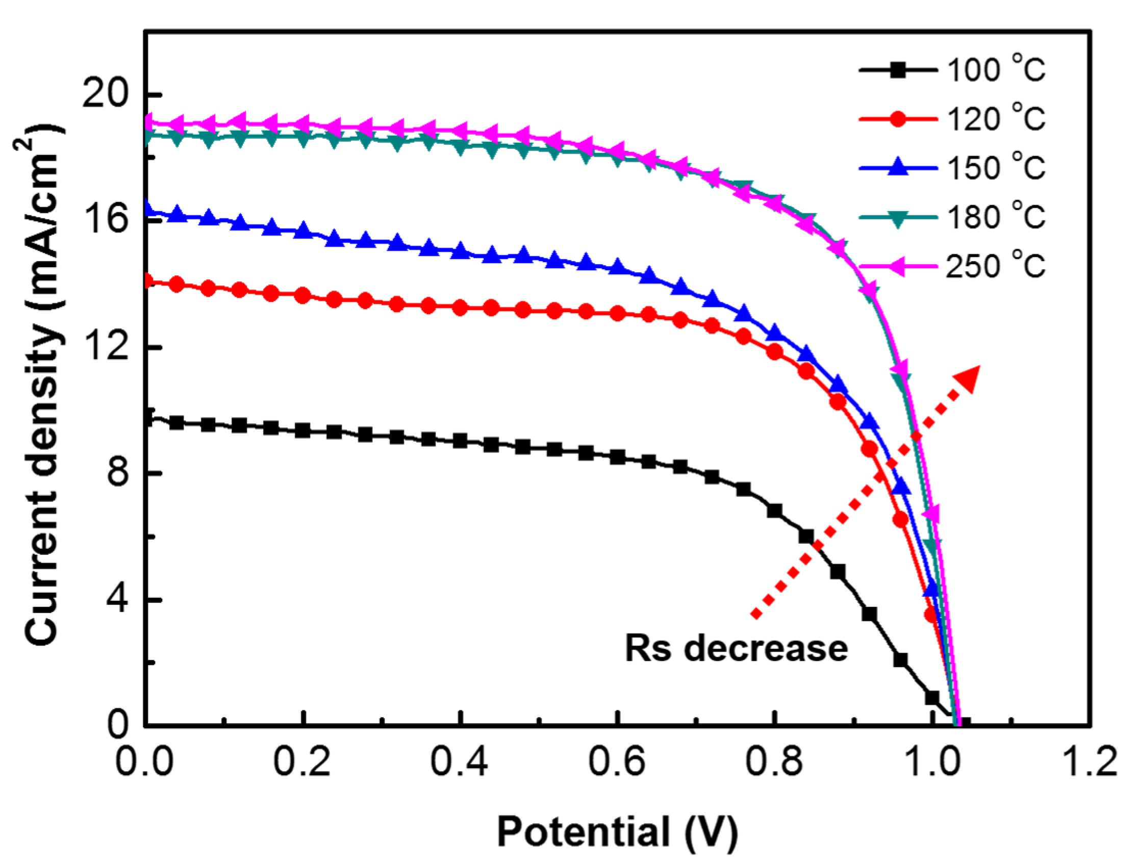
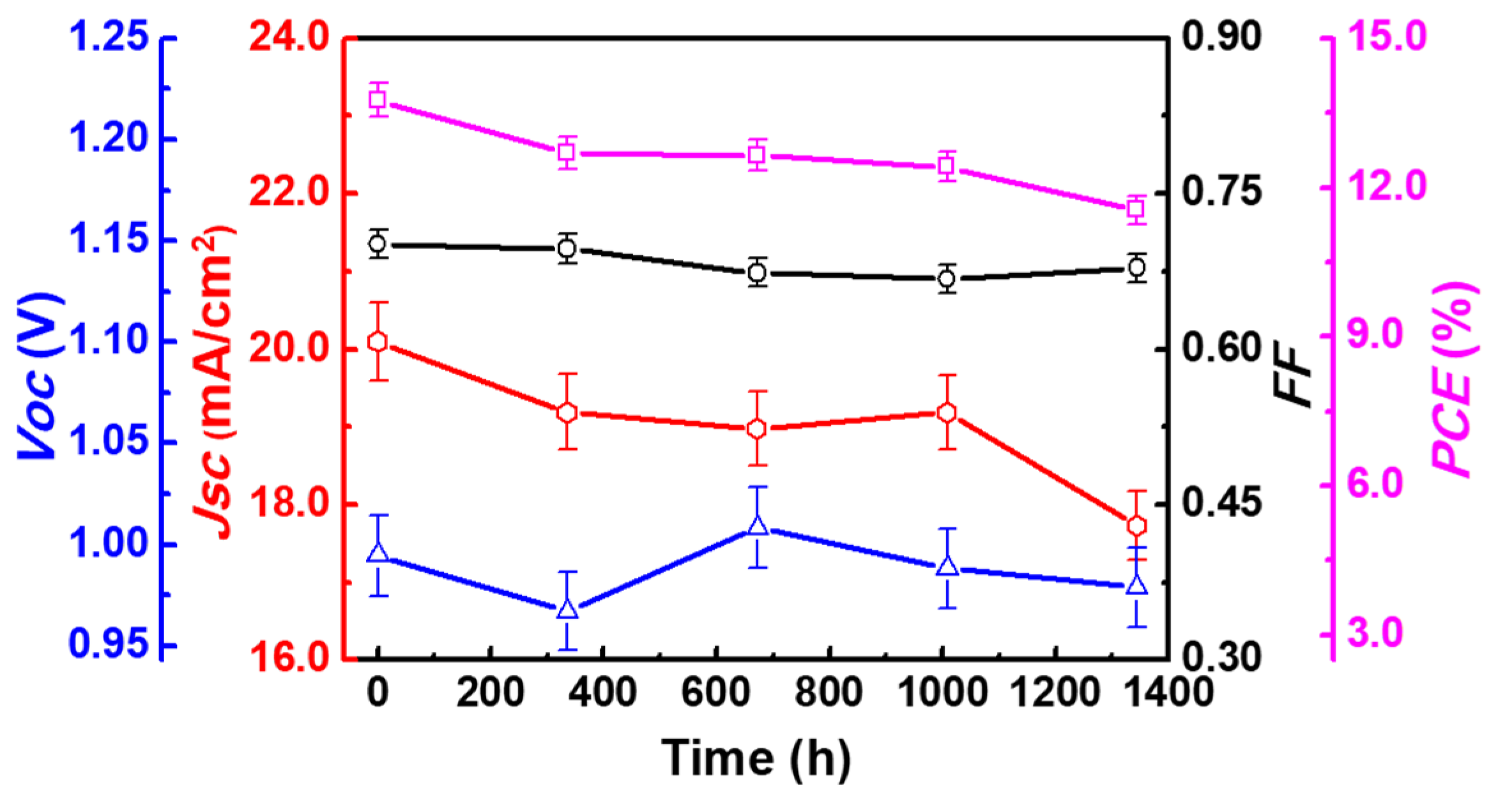
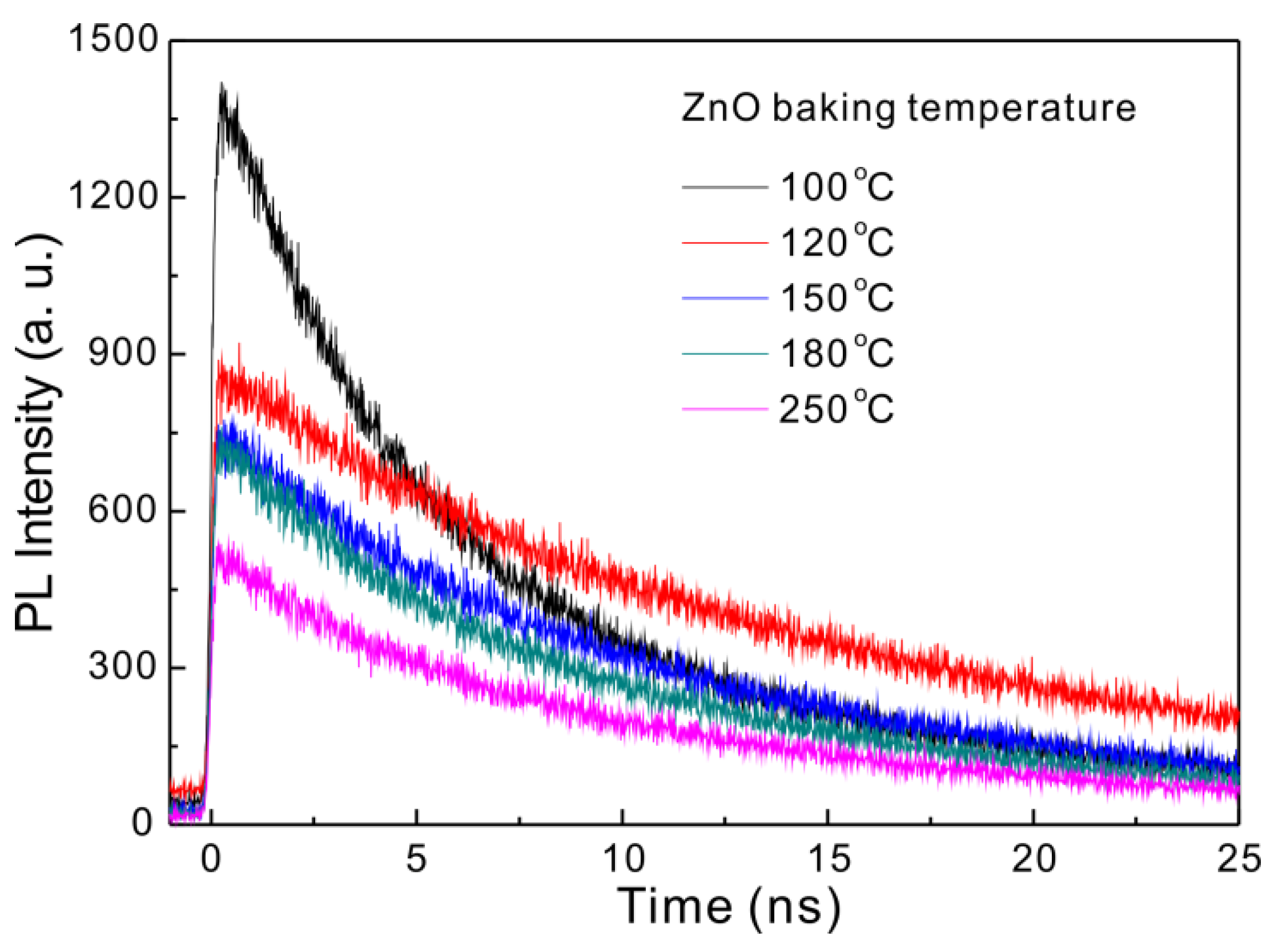
3.2. Influence of Baking Temperature

As mentioned in the introduction, the surface of ZnO can be modified by thermal annealing to remove the hydroxide. Therefore, the baking temperature of the ZnO electron transport layer is an important issue for the fabrication of the efficient ZnO-based PSCs. Here, the baking temperature of the ZnO electron transport layer was set at 100 °C, 120 °C, 150 °C, 180 °C, and 250 °C, respectively, and the baking time was fixed at 30 min. The AFM was used to observe the topography of the ZnO electron transport layers with respect to the various baking temperatures. The AFM topographic images were acquired in tapping mode over an area of 10 μm × 10 μm at a scanning speed of 2 MHz, as shown in Figure 5, where the various ZnO electron transport layers are compact and flat. Moreover, various ZnO electron transport layers with different baking temperatures usually show ~3 nm of root-mean-square roughness value, which benefits subsequent layers, such as MAPbI3 and Spiro-MeOTAD. The flatter surface contributes to the full coverage of the MAPbI3 and Spiro-MeOTAD layers and their molecular arrangements.
The time-resolved photoluminescence decays (TRPL) of the MAPbI3/ZnO/FTO glass with different baking temperatures are shown in Figure 6. The lifetimes of the excitons for samples baking at 100 °C, 120 °C, 150 °C, 180 °C, and 250 °C can be obtained by fitting the relaxation curves with a constant exponentially decaying function: 5.81 ns, 13.81 ns, 10.45 ns, 8.66 ns, and 9.36 ns, respectively. At the baking temperature of 100 °C, the sample had the largest PL intensity at the initial time (t = 0), and this indicates that the interface between the ZnO electron transport layer and MAPbI3 shows the lowest efficiency of exciton dissociation, which results in the smallest short current density. When the ZnO film baking temperature was increased from 120 to 180 °C, the lifetime of excitons was reduced from 13.81 to 8.66 ns, which is due to the higher conductivity of the ZnO electron transport layer. In accordance with the Onsager–Braun theory, the efficiency of the exciton dissociation at the interface between MAPbI3 and the ZnO electron transport layer increases with the conductivity (electron mobility) of the ZnO electron transport layer [36].
The J-V curves of perovskite-structured photovoltaic devices based on various ZnO electron transport layers with different baking temperatures are shown in Figure 7. The series resistance (RS) of ZnO-based perovskite photovoltaic device decreases when the baking temperature is increased, which reveals that the interface resistances of ZnO/perovskite and the conductivity of the ZnO electron transport layer improved when the baking temperature was increased from 100 to 180 °C. When the baking temperature was higher than 250 °C, the shunt resistance (Rsh) of the perovskite photovoltaic device decreased, as a result of the formation of the pinholes in the ZnO electron transport layer. In our previous work [20], it was shown that the short-circuit current density of perovskite photovoltaic devices was proportional to the efficiency of the exciton dissociation at the interface between the perovskite layer and the ZnO electron transport layer, and this could be evaluated by nanosecond TRPL spectroscopy. Table 1 summarizes the photovoltaic performances of various ZnO-based PSCs with different baking temperatures of ZnO electron transport layers.
Finally, the stability of the highest performance ZnO-based PSC without encapsulation was investigated as a function of time and is shown in Figure 8. The devices were placed in the dark at 5.0% RH and 25 °C and present a slight decay in performance after 1300 h. This reveals that ZnO films in an optimized thermal treatment process, in order to avoid the formation of hydroxide or acetate ligands, have an excellent ZnO/perovskite interface, resulting in a PSC with high efficiency and stability, which may confirm Kelly’s group report [29]. The performance decay is due to the decrease in the short circuit current density (JSC), which declined from 20 to 18 mA/cm2. On the contrary, the VOC is found to be remarkably stable. The degradation of the JSC may also originate from the migration of iodine ions in the perovskite film, leading to an oxidation of the metallic contact and current loss. Another reason could be the leakage of additives in the spiro-MeOTAD, causing a progressive decrease in conductivity, as this compound has been identified as one of the main sources of instability in the solar cell. Moreover, an increase in contact resistance occurs due to the partial peel of Ag electrodes after several device measurements. These devices will be fabricated well with encapsulation and welding wires in further experiments in order to fully understand the degradation mechanism of PSCs at accelerated aging test conditions.

4. Conclusions

The photovoltaic performance is explored here by a planar heterojunction perovskite-structured solar cell with a ZnO/CH3NH3PbI3/Spiro-MeOTAD/MoO3/Ag configuration. We carried out a detailed study on a ZnO electron transport layer and considered film thickness, surface morphology, crystallinity, post-baking temperatures, and PL properties, which are critical parameters for improving the performance of ZnO-based perovskite-structured photovoltaic devices. The highest-performing device exhibited a power conversion efficiency of about 13.66% when it was prepared with a ZnO thickness of ~20 nm and a post-baking temperature of 180 °C for 30 min. This is partly due to the highly conductive nature of ZnO thin films. Finally, the device performances stay remarkably constant for more than 1300 h stored in dark and dry conditions.

Acknowledgments

The authors acknowledge the financial support of the Ministry of Science and Technology, Taiwan (grand number: MOST 104-2731-M-182-001-MY2, MOST 106-2218-E-182-005-MY2, and MOST 106-2221-E-182-057-MY3), and the financial support of the Chang Gung Memorial Hospital, Linkou, Taiwan (CMRPD2F0161 and BMRPC074).

Author Contributions

Kun-Mu Lee and Ming-Chung Wu conceived and designed the experiments; Yin-Hsuan Chang and Ting-Han Lin performed the experiments; Ting-Han Lin and Chuan-Jung Lin analyzed the data; Kun-Mu Lee and Vembu Suryanarayanan wrote the paper.

Conflicts of Interest

The authors declare no conflicts of interest.

References

  1. Burschka, J.; Pellet, N.; Moon, S.-J.; Humphry-Baker, R.; Gao, P.; Nazeeruddin, M.K.; Graetzel, M. Sequential deposition as a route to high-performance perovskite-sensitized solar cells. Nature 2013, 499, 316–319. [Google Scholar] [CrossRef] [PubMed]
  2. Xing, G.; Mathews, N.; Sun, S.; Lim, S.S.; Lam, Y.M.; Graetzel, M.; Mhaisalkar, S.; Sum, T.C. Long-range balanced electron- and hole-transport lengths in organic-inorganic CH3NH3PbI3. Science 2013, 342, 344–347. [Google Scholar] [CrossRef] [PubMed]
  3. Lee, M.M.; Teuscher, J.; Miyasaka, T.; Murakami, T.N.; Snaith, H.J. Efficient hybrid solar cells based on meso-superstructured organometal halide perovskites. Science 2012, 338, 643–647. [Google Scholar] [CrossRef] [PubMed]
  4. Chen, Y.; He, M.; Peng, J.; Sun, Y.; Liang, Z. Structure and growth control of organic-inorganic halide perovskites for optoelectronics: From polycrystalline films to single crystals. Adv. Sci. 2016, 3, 1500392. [Google Scholar] [CrossRef] [PubMed]
  5. Green, M.A.; Ho-Baillie, A.; Snaith, H.J. The emergence of perovskite solar cells. Nat. Photonics 2014, 8, 506–514. [Google Scholar] [CrossRef]
  6. Zhu, W.; Bao, C.; Wang, Y.; Li, F.; Zhou, X.; Yang, J.; Lv, B.; Wang, X.Y.; Yu, T.; Zou, Z. Coarsening of one-step deposited organolead triiodide perovskite films via Ostwald ripening for high efficiency planar-heterojunction solar cells. Dalton Trans. 2016, 45, 7856–7865. [Google Scholar] [CrossRef] [PubMed]
  7. Kojima, A.; Teshima, K.; Shirai, Y.; Miyasaka, T. Organometal halide perovskites as visible-light sensitizers for photovoltaic cells. J. Am. Chem. Soc. 2009, 131, 6050–6051. [Google Scholar] [CrossRef] [PubMed]
  8. Im, J.-H.; Lee, C.-R.; Lee, J.-W.; Park, S.-W.; Park, N.-G. 6.5% efficient perovskite quantum-dot-sensitized solar cell. Nanoscale 2011, 3, 4088–4093. [Google Scholar] [CrossRef] [PubMed]
  9. Yang, W.S.; Park, B.-W.; Jung, E.H.; Jeon, N.J.; Kim, Y.C.; Lee, D.U.; Shin, S.S.; Seo, J.; Kim, E.K.; Noh, J.H.; et al. Iodide management in formamidinium-lead-halide-based perovskite layers for efficient solar cells. Science 2017, 356, 1376–1379. [Google Scholar] [CrossRef] [PubMed]
  10. Matas Adams, A.; Marin-Beloqui, J.M.; Stoica, G.; Palomares, E. The influence of the mesoporous TiO2 scaffold on the performance of methyl ammonium lead iodide (MAPI) perovskite solar cells: Charge injection, charge recombination and solar cell efficiency relationship. J. Mater. Chem. A 2015, 3, 22154–22161. [Google Scholar] [CrossRef]
  11. Wang, H.-H.; Chen, Q.; Zhou, H.; Song, L.; Louis, Z.S.; Marco, N.D.; Fang, Y.; Sun, P.; Song, T.-B.; Chen, H.; et al. Improving the TiO2 electron transport layer in perovskite solar cells using acetylacetonate-based additives. J. Mater. Chem. A 2015, 3, 9108–9115. [Google Scholar] [CrossRef]
  12. Hadouchi, W.; Rousset, J.; Tondelier, D.; Geffroy, B.; Bonnassieux, Y. Zinc oxide as a hole blocking layer for perovskite solar cells deposited in atmospheric conditions. RSC Adv. 2016, 6, 67715–67723. [Google Scholar] [CrossRef]
  13. Ahmed, M.I.; Hussain, Z.; Mujahid, M.; Khan, A.N.; Javaid, S.S.; Habib, A. Low resistivity ZnO-GO electron transport layer based CH3NH3PbI3 solar cells. AIP Adv. 2016, 6, 065303. [Google Scholar] [CrossRef]
  14. Li, C.; Zang, Z.; Han, C.; Hu, Z.; Tang, X.; Du, J.; Leng, Y.; Sun, K. Highly compact CsPbBr3 perovskite thin films decorated by ZnO nanoparticles for enhanced random lasing. Nano Energy 2017, 40, 195–202. [Google Scholar] [CrossRef]
  15. Zhang, L.; Yang, X.; Jiang, Q.; Wang, P.; Yin, Z.; Zhang, X.; Tan, H.; Yang, Y.; Wei, M.; Sutherland, B.R.; et al. Ultra-bright and highly efficient inorganic based perovskite light-emitting diodes. Nat. Commun. 2017, 8, 15640. [Google Scholar] [CrossRef] [PubMed]
  16. Park, H.-Y.; Lim, D.; Kim, K.-D.; Jang, S.-Y. Performance optimization of low-temperature-annealed solution-processable zno buffer layers for inverted polymer solar cells. J. Mater. Chem. A 2013, 1, 6327–6334. [Google Scholar] [CrossRef]
  17. Xu, L.; Guo, Y.; Liao, Q.; Zhang, J.; Xu, D. Morphological control of ZnO nanostructures by electrodeposition. J. Phys. Chem. B 2005, 109, 13519–13522. [Google Scholar] [CrossRef] [PubMed]
  18. Carcia, P.; McLean, R.; Reilly, M. High-performance ZnO thin-film transistors on gate dielectrics grown by atomic layer deposition. Appl. Phys. Lett. 2006, 88, 3509. [Google Scholar] [CrossRef]
  19. Dong, X.; Hu, H.; Lin, B.; Ding, J.; Yuan, N. The effect of ALD-ZnO layers on the formation of CH3NH3PbI3 with different perovskite precursors and sintering temperatures. Chem. Commun. 2014, 50, 14405–14408. [Google Scholar] [CrossRef] [PubMed]
  20. Lee, K.-M.; Chang, S.H.; Wang, K.-H.; Chang, C.-M.; Cheng, H.-M.; Kei, C.-C.; Tseng, Z.-L.; Wu, C.-G. Thickness effects of ZnO thin film on the performance of tri-iodide perovskite absorber based photovoltaics. Sol. Energy 2015, 120, 117–122. [Google Scholar] [CrossRef]
  21. Liu, D.; Yang, J.; Kelly, T.L. Compact layer free perovskite solar cells with 13.5% efficiency. J. Am. Chem. Soc. 2014, 136, 17116–17122. [Google Scholar] [CrossRef] [PubMed]
  22. Song, J.; Liu, L.; Wang, X.-F.; Chen, G.; Tian, W.; Miyasaka, T. Highly efficient and stable low-temperature processed ZnO solar cells with triple cation perovskite absorber. J. Mater. Chem. A 2017, 5, 13439–13447. [Google Scholar] [CrossRef]
  23. Han, G.S.; Shim, H.-W.; Lee, S.; Duff, M.L.; Lee, J.-K. Low-temperature modification of ZnO nanoparticles film for electron-transport layers in perovskite solar cells. Chemsuschem 2017, 10, 2425–2430. [Google Scholar] [CrossRef] [PubMed]
  24. Liu, D.; Kelly, T.L. Perovskite solar cells with a planar heterojunction structure prepared using room-temperature solution processing techniques. Nat. Photonics 2014, 8, 133–138. [Google Scholar] [CrossRef]
  25. Zhang, J.; Pauporté, T. Effects of oxide contact layer on the preparation and properties of CH3NH3PbI3 for perovskite solar cell application. J. Phys. Chem. C 2015, 119, 14919–14928. [Google Scholar] [CrossRef]
  26. Shin, S.S.; Yang, W.S.; Noh, J.H.; Suk, J.H.; Jeon, N.J.; Park, J.H.; Kim, J.S.; Seong, W.M.; Seok, S.I. High-performance flexible perovskite solar cells exploiting Zn2SnO4 prepared in solution below 100 °C. Nat. Commun. 2015, 6, 7410. [Google Scholar] [CrossRef] [PubMed]
  27. Mahmud, M.A.; Elumalai, N.K.; Upama, M.B.; Wang, D.; Chan, K.H.; Wright, M.; Xu, C.; Haque, F.; Uddin, A. Low temperature processed ZnO thin film as electron transport layer for efficient perovskite solar cells. Sol. Energy Mater. Sol. Cells 2017, 159, 251–264. [Google Scholar] [CrossRef]
  28. Cheng, Y.; Yang, Q.-D.; Xiao, J.; Xue, Q.; Li, H.-W.; Guan, Z.; Yip, H.-L.; Tsang, S.-W. Decomposition of organometal halide perovskite films on zinc oxide nanoparticles. ACS Appl. Mater. Interfaces 2015, 7, 19986–19993. [Google Scholar] [CrossRef] [PubMed]
  29. Yang, J.; Siempelkamp, B.D.; Mosconi, E.; De Angelis, F.; Kelly, T.L. Origin of the thermal instability in CH3NH3PbI3 thin films deposited on ZnO. Chem. Mater. 2015, 27, 4229–4236. [Google Scholar] [CrossRef]
  30. Zang, Y.; Li, C.-Z.; Chueh, C.-C.; Williams, S.T.; Jiang, W.; Wang, Z.-H.; Yu, J.-S.; Jen, A.K.Y. Integrated molecular, interfacial, and device engineering towards high-performance non-fullerene based organic solar cells. Adv. Mater. 2014, 26, 5708–5714. [Google Scholar] [CrossRef] [PubMed]
  31. IEC 60904:2017 Series Photovoltaic Devices—All Parts; International Electrotechnical Commission: London, UK, 2017.
  32. Song, J.; Bian, J.; Zheng, E.; Wang, X.-F.; Tian, W.; Miyasaka, T. Efficient and environmentally stable perovskite solar cells based on ZnO electron collection layer. Chem. Lett. 2015, 44, 610–612. [Google Scholar] [CrossRef]
  33. Sum, T.C.; Mathews, N. Advancements in perovskite solar cells: Photophysics behind the photovoltaics. Energy Environ. Sci. 2014, 7, 2518–2534. [Google Scholar] [CrossRef]
  34. David, C.L.; Kevin, D.L.; Darren, B.T.; Buguo, W. High conductance in ultrathin films of ZnO. Jpn. J. Appl. Phys. 2014, 53, 05FJ01. [Google Scholar]
  35. Li, Y.; Yan, W.; Li, Y.; Wang, S.; Wang, W.; Bian, Z.; Xiao, L.; Gong, Q. Direct observation of long electron-hole diffusion distance in CH3NH3PbI3 perovskite thin film. Sci. Rep. 2015, 5, 14485. [Google Scholar] [CrossRef] [PubMed]
  36. Deibel, C.; Strobel, T.; Dyakonov, V. Origin of the efficient polaron-pair dissociation in polymer-fullerene blends. Phys. Rev. Lett. 2009, 103, 036402. [Google Scholar] [CrossRef] [PubMed]
Figure 1. (a) The construction of the perovskite solar cell (PSC), and (b) the energy level diagram of materials used in the perovskite photovoltaic device in this study.
Coatings 07 00215 g001
Figure 2. Various ZnO electron transport layers spin-coated on the FTO glass: (a) Bare FTO; (b) one layer; (c) two layers; (d) three layers; (e) four layers; and (f) five layers.
Coatings 07 00215 g002
Figure 3. The XRD patterns of various ZnO electron transport layers, baking at 180 °C.
Coatings 07 00215 g003
Figure 4. PL spectra of perovskite films with various ZnO electron transport layers on a bare glass substrate, baking at 180 °C.
Coatings 07 00215 g004
Figure 5. AFM images of the ZnO electron transport layer (~20 nm) with different baking temperatures: (a) 100 °C; (b) 120 °C; (c) 150 °C; (d) 180 °C; and (e) 250 °C.
Coatings 07 00215 g005
Figure 6. The time-resolved photoluminescence decays of MAPbI3/ZnO (~20 nm)/FTO glass with the different baking temperatures.
Coatings 07 00215 g006
Figure 7. The J-V curves of perovskite photovoltaic devices based on ZnO layer with different baking temperatures.
Coatings 07 00215 g007
Figure 8. Stability of the ZnO-based perovskite photovoltaic device stored in a dark condition (5.0% RH and 25 °C).
Coatings 07 00215 g008
Table 1. The photovoltaic performances and carrier lifetime of MAPbI3 solar cell with different baking temperatures of the ZnO electron transport layer.
Baking Temp. (°C)VOC (V)JSC (mA/cm2)FF (%)Efficiency (%)Lifetime (ns)
1001.058.8156.05.185.81
1201.0314.0965.39.4713.81
1501.0316.3559.210.4910.45
1801.0418.7170.213.668.66
2501.0319.1267.813.349.36

