Article

A 300-mV ΔΣ Modulator Using a Gain-Enhanced, Inverter-Based Amplifier for Medical Implant Devices

by
Ali Fazli Yeknami
School of Electrical Engineering and Computer Science, Oregon State University, 1148 Kelley Engineering Center, Corvallis, OR 97331, USA
J. Low Power Electron. Appl. 2016, 6(1), 4; https://doi.org/10.3390/jlpea6010004
Submission received: 30 September 2015 / Revised: 2 March 2016 / Accepted: 8 March 2016 / Published: 11 March 2016
(This article belongs to the Special Issue Implantable Bio-Electronic Circuits and Systems)

Abstract

:
An ultra-low-voltage low-power switched-capacitor (SC) delta-sigma (ΔΣ) modulator running at a supply voltage as low as 300 mV is presented for biomedical implant devices, e.g., cardiac pacemakers. To reduce the supply voltage, an inverter-based amplifier is used in the integrators, whose DC gain and gain-bandwidth (GBW) are boosted by a simple current-mirror output stage. The full input-feedforward loop topology offers low integrators internal swing, supporting ultra-low-voltage operation. To demonstrate the concept, a second-order loop topology was chosen. The entire modulator operates reliably against process, voltage and temperature (PVT) variations from a 300 mV ± 10% supply voltage only, while the switches are driven by a charge pump clock boosting scheme. Designed in a 65 nm CMOS technology and clocked at 256 kHz, the simulation results show that the modulator can achieve a 64.4 dB signal-to-noise ratio (SNR) and a 60.7 dB signal-to-noise and distortion ratio (SNDR) over a 1.0 kHz signal bandwidth while consuming 0.85 μW of power.

1. Introduction

Supply voltage reduction, as a direct consequence of the process technologies’ scaling, is further enforced by battery-operated biomedical implant devices, such as pacemakers, cardiac defibrillators and neural recording integrated circuits, to make their operating supply compatible with human body potentials [1,2], in the range of few hundreds of mVs. Therefore, designing analogue-to-digital converters (ADCs) operating at a very low supply voltage is inevitable for the measurement of various electrophysiological signals (e.g., ECGs, EEGs, etc.).
Pacemakers need to sense the cardiac signals, which mainly are situated in very low frequencies from nearly DC to several hundred hertz [3,4,5,6,7]. The cardiac signals are sensed by the low-noise amplifier, amplified by a gain stage; the undesired interferences are filtered out, and then, the detected analog signal is digitized by a back-end ADC. The ADC architecture and circuit design play a key role in maintaining ultra-low-power efficiency while providing a high conversion accuracy (or resolution). ADC resolutions from eight bit to 13 bit have been reported previously [5,6,7]. The low frequency noise, including flicker noise, needs to be treated properly in the circuit implementation.
There are two critical factors that can determine the lowest operating power supply of the traditional sigma-delta (ΔΣ) modulators: operational transconductance amplifiers (OTAs) in the integrators and the adequate driving voltage of the switching transistors [8,9,10,11,12,13,14]. The conventional analog circuit topologies are no longer practical in ultra-low-voltage operations (below 0.6 V), and also, stacking more than two transistors is impossible due to the limited overdrive and voltage headroom. The inverter is the simplest amplifier, which can sustain a supply voltage of less than the sum of the absolute threshold voltages of the NMOS and PMOS transistors [12], also known as a Class-C inverter. The DC gain and gain-bandwidth product (GBW) of the CMOS inverter degrade significantly at supplies far below the nominal VTN + |VTP| = 0.62 V and need to be enhanced for a robust and high-performance modulator design. Chae and Han [12] proposed an inverter-based ΔΣ modulator using a cascode inverter for boosting the DC gain. In this paper, we present a fully-differential second-order feedforward ΔΣ modulator for ultra-low-voltage low-power biomedical applications, which uses a novel gain-enhanced inverter-based, current mirror amplifier to replace the OTA in the integrators. Moreover, a clock boosting scheme is used to sufficiently drive the switching transistors. While all transistors operate at gate voltage less than 300 mV, the effective gate voltage of the switches is 600 mV with the aid of a charge pump clock doubler [
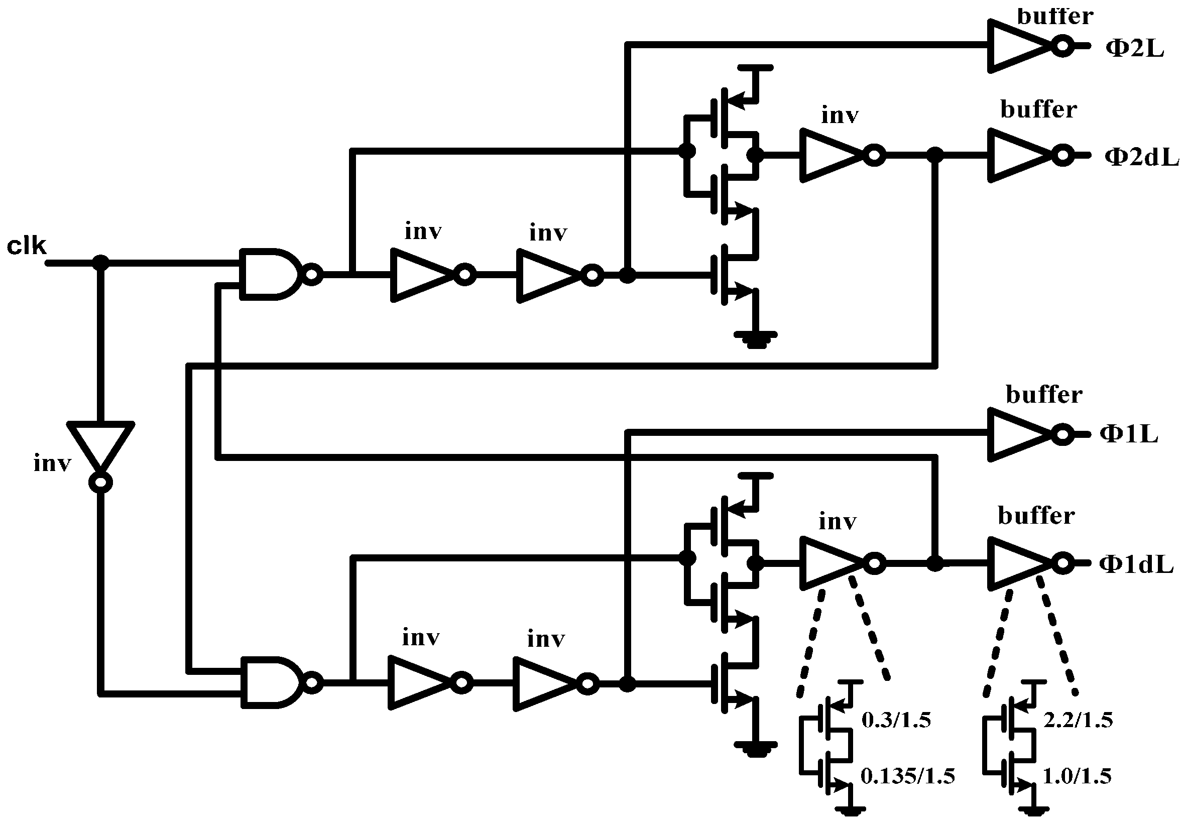
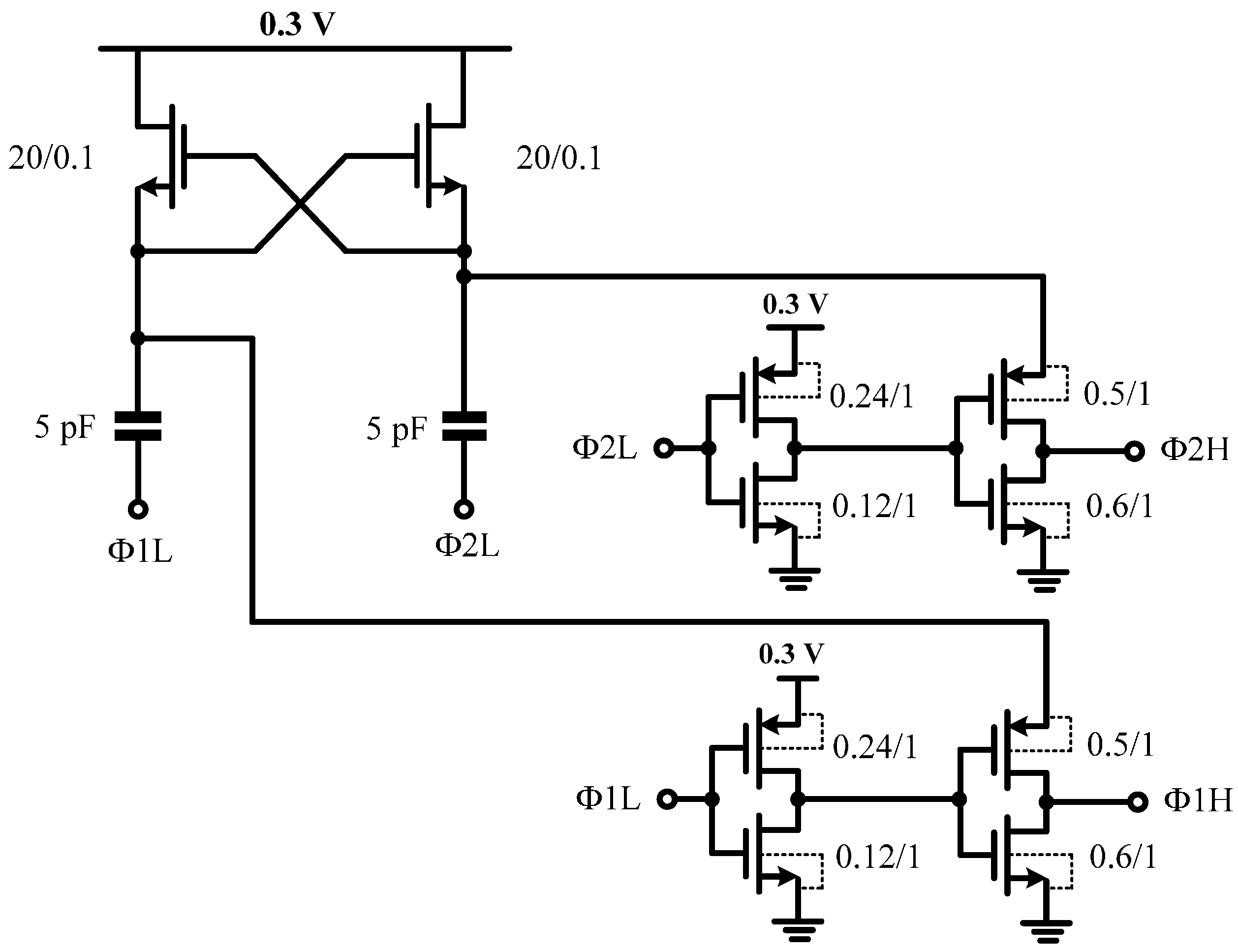
13]. The single-bit quantizer, including the preamplifier, dynamic comparator and latch, was designed in a deep sub-threshold regime, providing very high power efficiency.
The rest of the paper is organized as follows: Section 2 describes the proposed gain-enhanced inverter-based amplifier and its advantages and drawbacks. Section 3 discusses the modulator architecture and its low-voltage and low-power design considerations. Section 4 presents the modulator circuit design. Section 5 discusses the simulation results. In Section 6, the proposed modulator is compared to the reported state-of-the-art ultra-low-voltage modulators. Conclusions are drawn in Section 7.

2. Proposed Gain-Enhanced Inverter-Based OTA

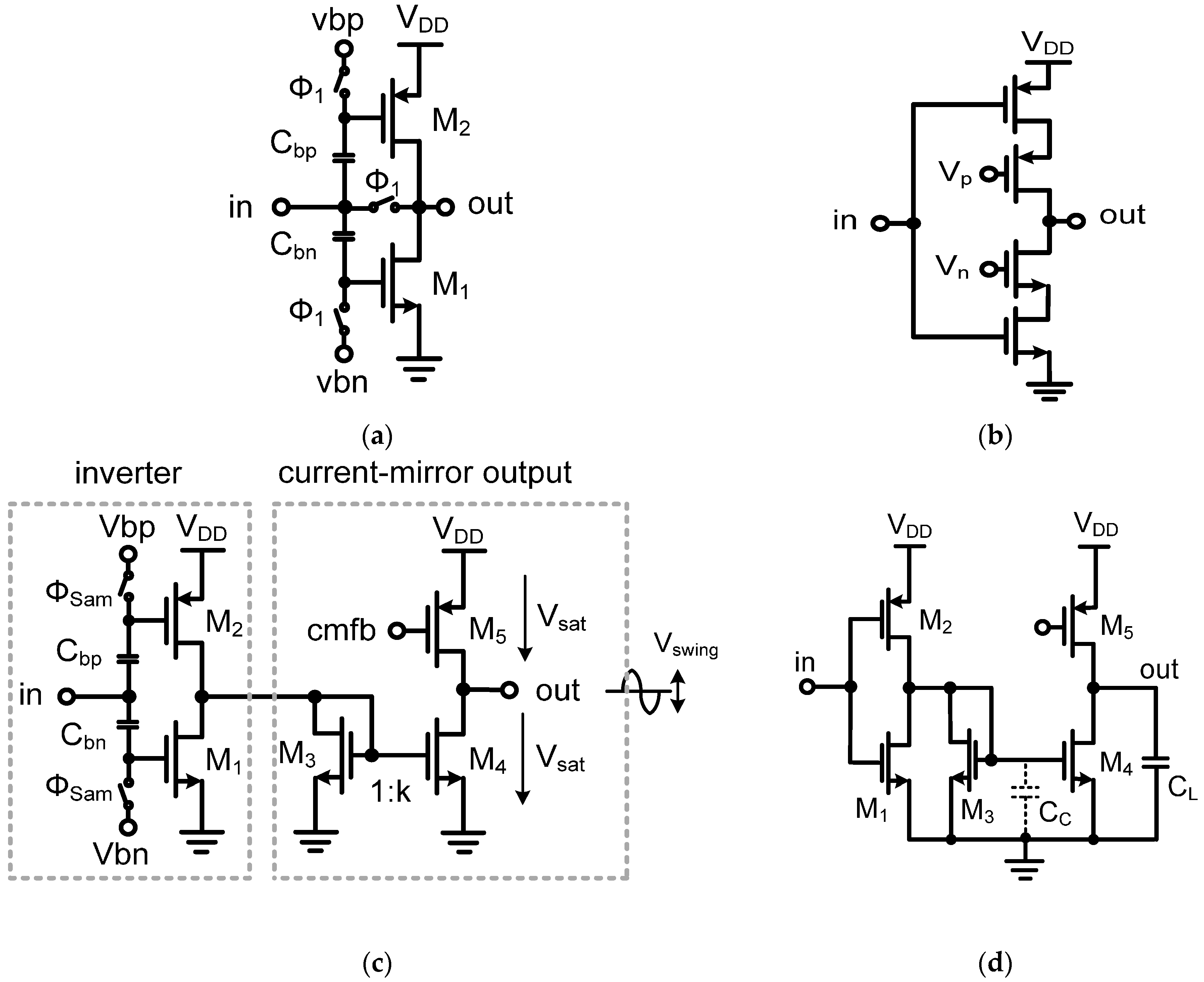
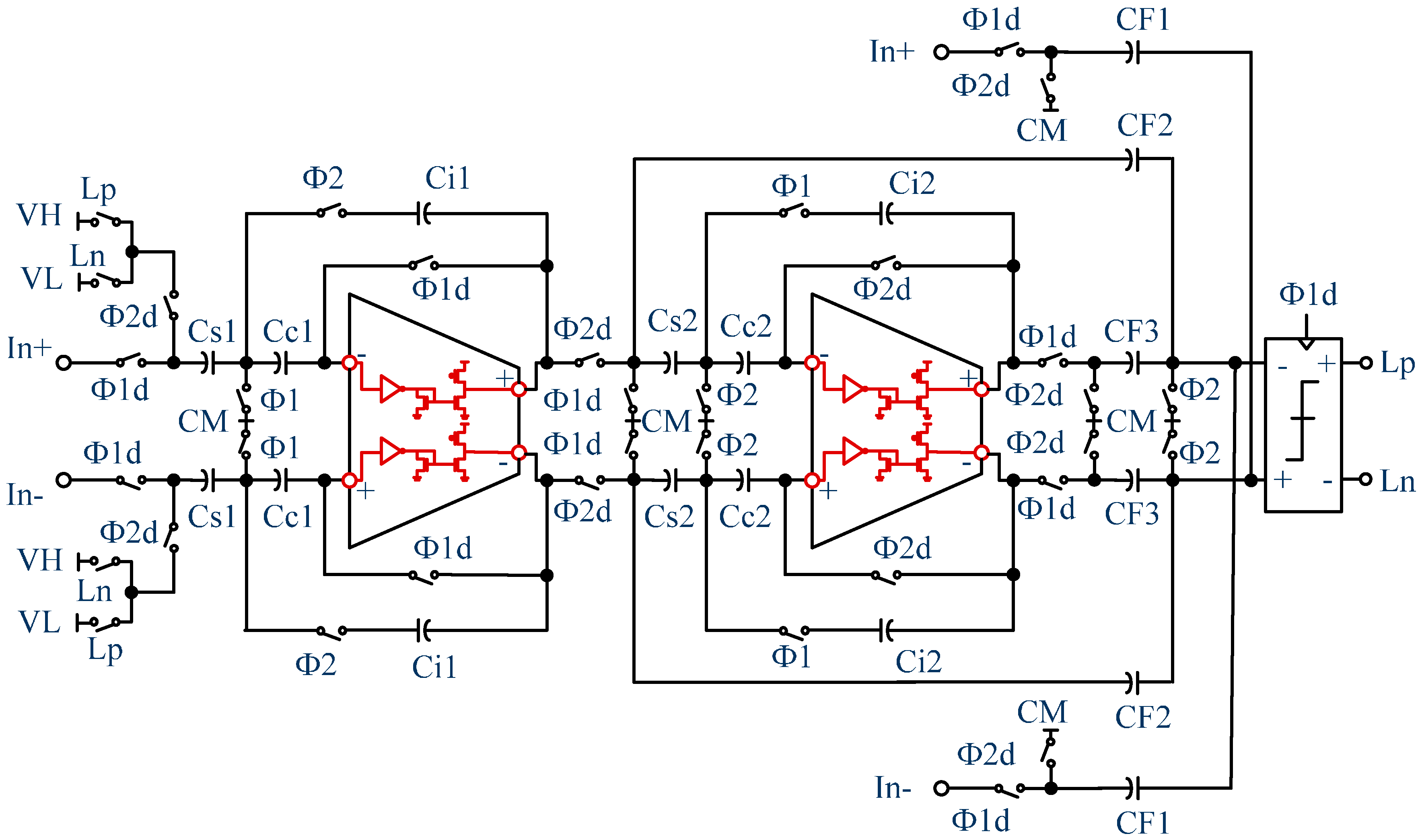
A novel inverter-based amplifier is proposed for ultra-low-voltage applications, which is composed of a Class-C inverter and a current mirror output stage. Figure 1 shows the schematics of the basic CMOS inverter, the cascode inverter and the proposed inverter-based, current mirror OTA (Figure 1c).
A switched-capacitor (SC) biasing scheme using floating capacitors Cbp and Cbn (Figure 1c) is used to define the operating point of the inverter M1–M2. These capacitors are periodically refreshed by the bias voltages Vbn and Vbp during the sampling phase ФSamSam = Ф1d in the first integrator; ФSam = Ф2d in the second integrator) and work as floating batteries between the input and the gates of the transistors. It is worth mentioning that the pre-charging Vbn and Vbp occurs simultaneously with sampling the signal onto CS1 (CS2) and the inverter offset onto CC1 (CC2) in phase ФSam (Figure 4). The sampling clock speed is low (i.e., 256 kHz), so initially, the Cbp = Cbn = 0.5 pF are charged in the early phase of ФSam (Cbp = Cbn << CCi), and then, the amplifier is placed in the unity feedback configuration for offset sampling when its biasing was set appropriately. The Vbp and Vbn are generated using a constant-gm biasing circuit followed by a level shifter to eliminate the Vsat problem as in [15], which provides wider overdrive voltage and, in turn, a smaller transistor width. At the output stage, an energy-efficient SC common-mode feedback (CMFB) circuit is employed [8], which derives the gate of PMOS transistor M5, in order to set the output CM level at the middle of the supply voltage for the maximum output swing.
The DC gain and GBW of the CMOS inverter degrade significantly at supplies far below the nominal VTN + |VTP|, which need to be enhanced for a robust and high-performance modulator design. The aim of the proposed technique is to boost the gain and GBW simultaneously by mirroring a small fraction (~10%) of the bias current of the inverter M1–M2 through transistor M3 to the output. The factor k is the current ratio of the current mirror M3–M4 and is defined as (W/L)M4/(W/L)M3. The approximate gain and GBW of the proposed amplifier shown in Figure 1c can be determined from its small-signal model using sub-threshold current as:
A e n = g m 1 + g m 2 g m 3 + g d s 1 + g d s 2 + g d s 3 . g m 4 g d s 4 + g d s 5
( g m 1 + g m 2 ) × k × R o u t
G B W = k × ( g m 1 + g m 2 ) 2 π C L = k ( 2 α ) I D 2 2 π C L n V T
where gmi and gdsi represent the transconductance and output conductance of the i-th transistor, respectively. Rout is the total output resistance, which is equal to (gds4 + gds5)−1. CL is the total load capacitor for the frequency compensation. n and VT are the sub-threshold parameters. We consider α = ID3/ID2 as the ratio of the currents of M3 and M2. In addition, it can be shown that the term gm4/(gm3 + gds1 + gds2 + gds3) is approximately equal to k. A large device size of M1–M2 has to be prevented, as it creates large parasitic capacitors, which can limit the amplifier speed.
To explain the gain-enhancement technique, the DC gain of the basic inverter (Figure 1a) and the proposed amplifier (Figure 1c) given by Equation (1) can be written in the following forms in Equations (3) and (6):
A 0 = ( g m 1 + g m 2 ) R o u t = 2 I D n V T × 1 λ I D = 2 n λ V T
VT is the thermal voltage; n is the non-ideality factor; and λ is the channel length modulation coefficient. A0 is the intrinsic gain achieved by an inverter in the sub-threshold regime. In deep submicron technologies, by shrinking the transistor length, the effect of channel length modulation becomes more important. As a consequence, the output resistance and, thus, the DC gain of the inverter are normally low.
In Figure 1c, the bias current of the diode-connected device (i.e., ID3) is equal to α ID2, where α in this design is approximately 0.1. The M1 transistor then shunts the rest of the current to the ground. Assuming M1 carries (1 − α) × ID2, from Equation (1), the gain of the proposed OTA can be expressed as:
A e n = ( g m 1 + g m 2 ) × k × R o u t = [ ( 1 α ) I D 2 n V T + I D 2 n V T ] × k × 1 λ 4 I D 4
Now, the biasing current of M4 is:
I D 4 = k × I D 3 = k × α I D 2
Finally, the enhanced gain of the OTA is given by:
A e n = 2 α 2 α × 2 n λ V T = ( 1 α 0.5 ) A 0
From Equation (6), it can be seen that the gain is enhanced (1/α − 0.5)-times. The gain increase can be adjusted by the α factor during the design. With α = 0.1 in this design, the gain can be enhanced 9.5-times directly from Equation (6). With α = ID3/ID2 as the ratio of the currents in M3 and M2, the current mismatch can affect the gain enhancement (Section 2.2). In typical corner simulation from a 0.3 V supply, the α factor is about 0.12, which corresponds to a gain enhancement of eight-times, whereas in the worst-case corner, it is approximately 0.13, corresponding to a gain enhancement of seven-times.
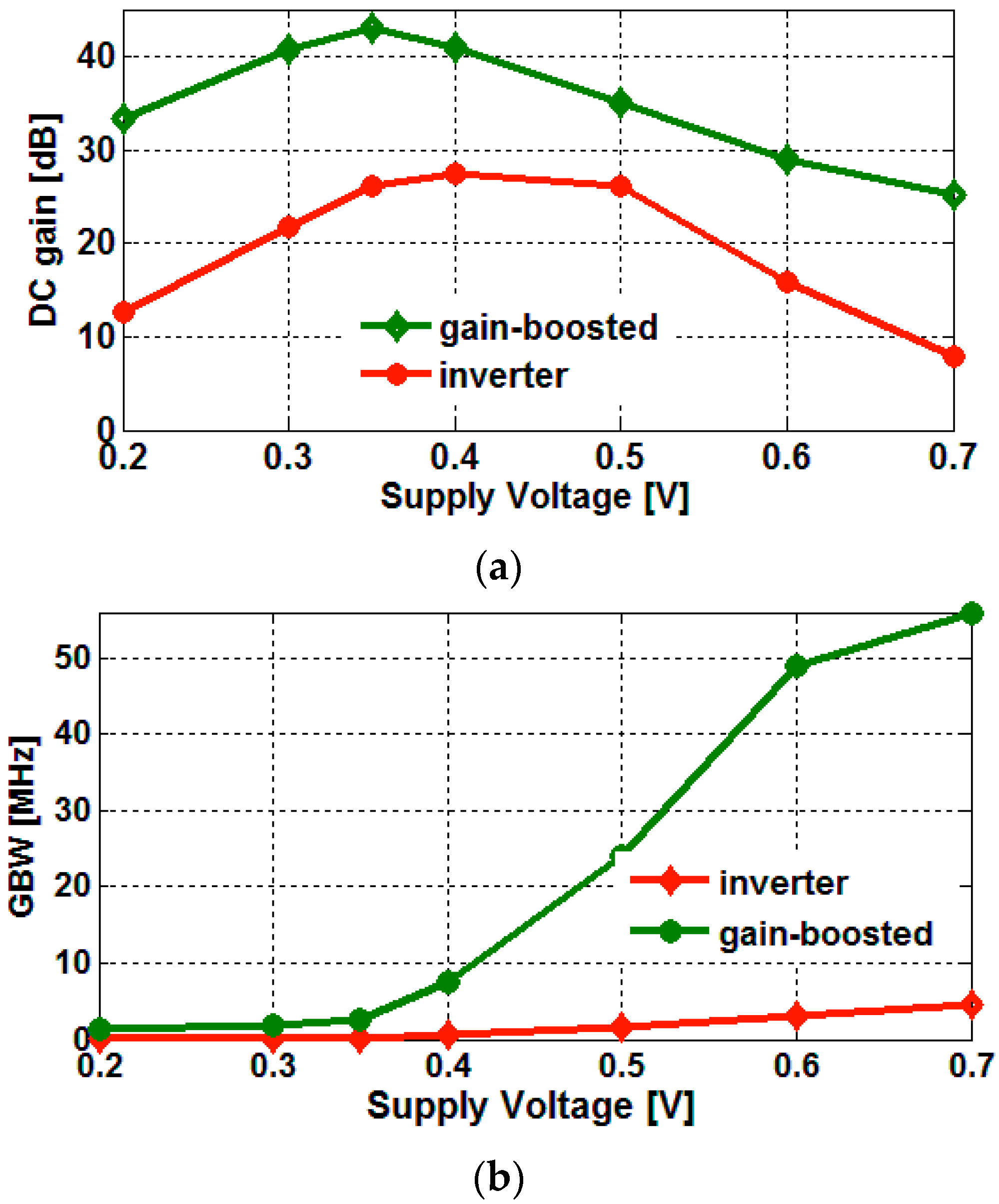
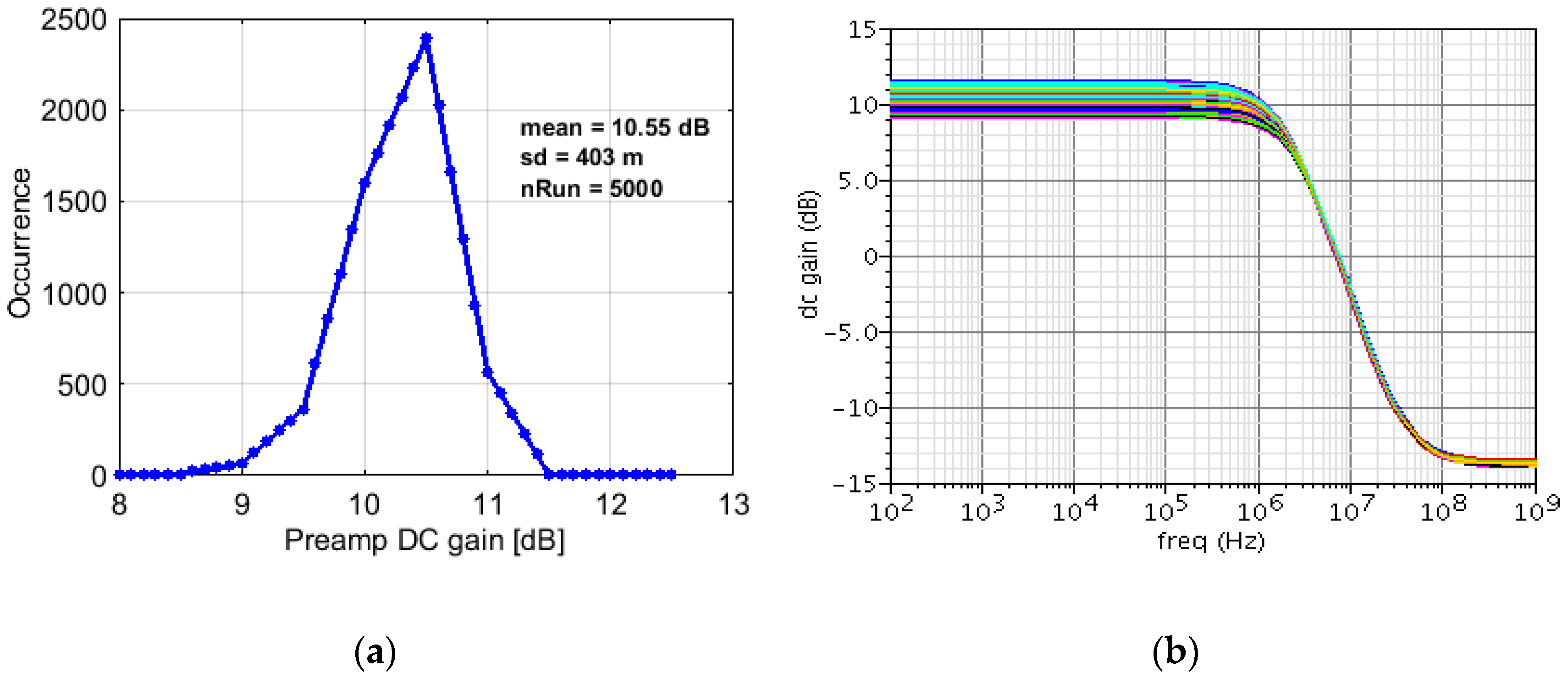
Figure 2a shows the variations of the DC gain with respect to the supply voltage (VDD) for the basic inverter shown in Figure 1a and the gain-enhanced inverter shown in Figure 1c. Figure 2b,c also shows the variations of the GBW as a function of the VDD for both the basic inverter and the gain-enhanced inverter. For PMOS transistor M2, the overdrive voltage (i.e., VDDVbp − |VTP|) depends on VDD and increases by increasing VDD. Similarly, for NMOS device M1, the overdrive voltage (i.e., VbnVTN) is enhanced linearly with VDD to accommodate a wider input linear range in this analysis.
For VDDs far below VTN + |VTP|, the DC gain and GBW degrade significantly. A large device size in M1–M2 has to be avoided, as this creates large parasitic capacitances, which can limit the OTA performance. The aim of this work is to enhance the gain and GBW simultaneously by mirroring a small fraction of the bias current of the inverter M1–M2 to the output stage (with α ~ 10% and k = 8).
Shown in Figure 2, with the current mirror gain-enhancement technique, the simulated DC gain and GBW increase to 40 dB and 1.9 MHz from 22 dB and 0.38 MHz, respectively, from a 0.3 V supply and a 3 pF load capacitance in a typical (TT) process corner, at 27 °C. The phase margin is 66 °C. The transistors sizes of the developed inverter-based current mirror amplifier are summarized in Table 1. The DC gain gets worse in FS (fast NMOS, slow PMOS) and SF (slow NMOS, fast PMOS) process corners (i.e., 37 dB at VDD = 0.3 V), whereas its deviation is trivial for FF and SS corners (i.e., 39 dB at VDD = 0.3 V).
In practice, the gain enhancement can be restricted by several factors: phase margin, matching of bias currents between the M1 and M3 transistors and thermal noise. These factors are discussed below.

2.1. Frequency Response and Internal Parasitic Pole

Using the gain-enhancement technique increases the impedance of the internal node at the gate of the diode-connected M3. The total parasitic capacitance at this node is represented by CP in Figure 1d. The parasitic non-dominant pole due to the impedance 1/gm3 of the transistor M3 operating in the sub-threshold regime and the parasitic capacitor CP can be expressed as:
P n d = g m 3 2 π C P = α I D 2 2 π C P n V T
where CP is approximately Cgs3 + Cgs4. To maintain a reasonably safe phase margin, the Pnd has to be placed more than three-times the unity GBW given by Equation (2). Thus, the following criteria for α can be derived with respect to CP/CL and k:
1 α 0.5 1 6 k C L C P
Recalling (1/α − 0.5) in Equation (6) as the gain-enhancement factor, Equation (8) represents the maximum gain-enhancement that can be achieved by the proposed technique. The larger the CL/CP, the greater is the gain enhancement and the phase margin, but this costs more power. The dominant pole in this design is set by CL, which can be expressed by:
P 1 = 1 2 π R o u t C L = g d s 4 + g d s 5 2 π C L

2.2. Bias Current Matching

As described earlier, the ratio of the bias currents of transistors M3 and M2, defined as α = ID3/ID2, plays an important role for enhancing the amplifier gain given by Equation (6). Practically, the matching between ID3 = α ID2 and ID1 = (1 − α) ID2 determines the real α factor and, thus, the gain enhancement. To ensure good matching between those currents, the gate bias voltages of M1–M2 both are generated from the same reference current source using current mirrors. For good matching, transistors should be sized properly.

2.3. Thermal Noise

A drawback of the gain-enhanced, inverter-based amplifier, as compared to the basic CMOS inverter, is that it exhibits more input-referred thermal noise, related to the gm3 of the device M3. Since the correlated double-sampling (CDS) technique, as an auto-zeroing technique, is used in the corresponding integrator, the low frequency flicker noise is attenuated at the cost of an increased white noise floor due to the noise folding accompanied by the sampling [16]. The foldover thermal noise of the integrator is the dominant source of the noise, in which the thermal noise is amplified by a factor GBW/fS, with sampling frequency fS [16]. As a result, the input-referred noise power of the Class-C inverter and the gain-enhanced inverter shown in Figure 1c, denoted by GE-inv, can be expressed, respectively, as:
V n f o l d , i n v 2 ¯ = G B W f s . 4 k T γ g m 1 + g m 2 [ v 2 / H z ]
V n f o l d , G E i n v 2 ¯ = G B W f s . 4 k T γ g m 1 + g m 2 ( 1 + g m 3 g m 1 + g m 2 ) [ v 2 / H z ]
where the noise of the gain-enhanced amplifier has an additional term corresponding to gm3. Therefore, M3 has to be sized carefully, such that the thermal noise is minimized and the non-dominant pole, i.e., gm3/2πCP with CP the parasitic capacitance at the gate of M3 and M4, is placed more than 3× the GBW for a reasonably safe phase margin.

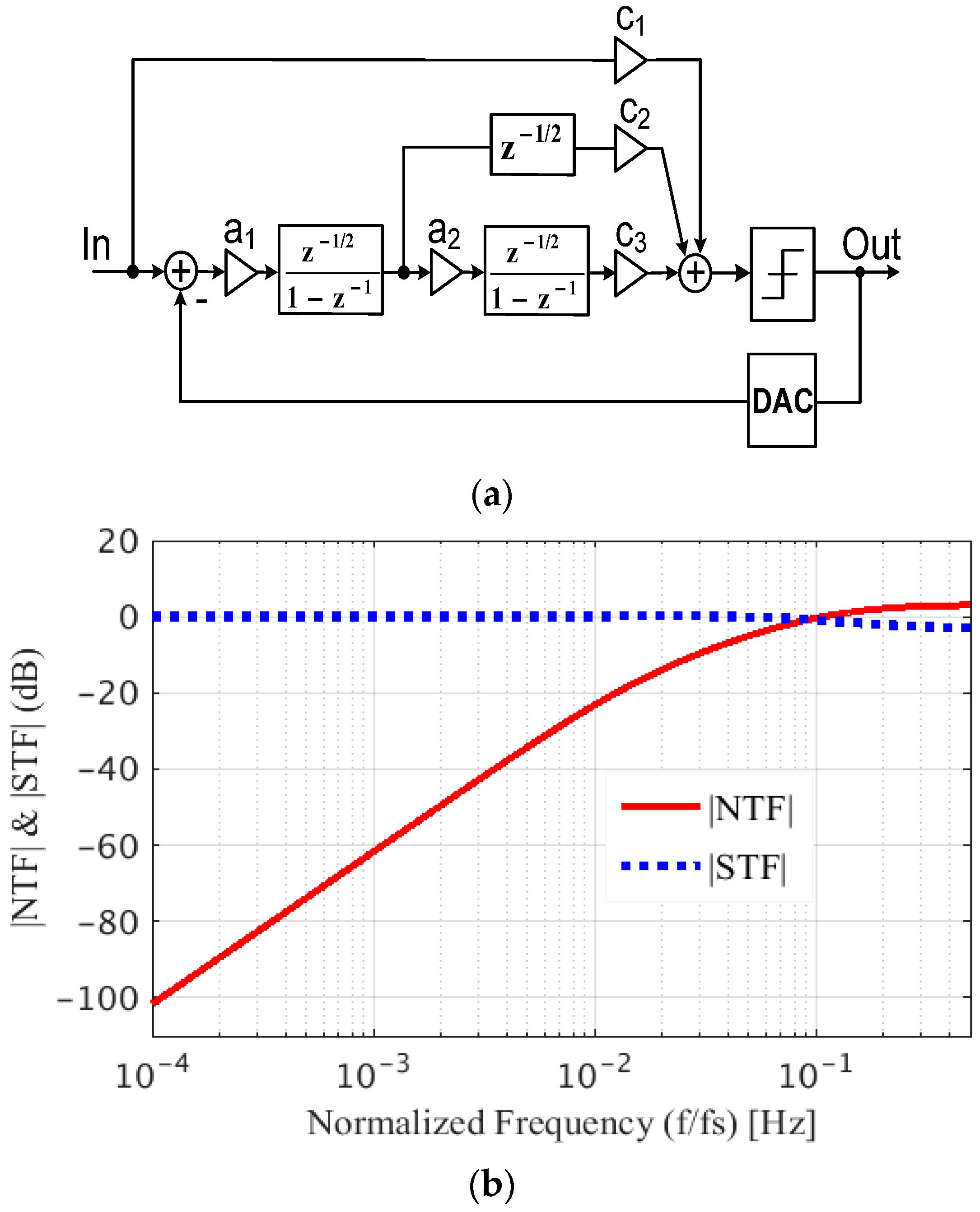
3. Modulator Architecture

Output swing is of great importance in ultra-low-voltage low-power designs, which directly determines the modulator dynamic range (DR) and, ultimately, the power consumption. The minimum swing Vswing that the amplifier shown in Figure 1c can still operate with imposes a hard limit equal to 2Vsat + Vswing for the supply voltage scaling, with saturation voltage Vsat. The limited voltage swing is therefore translated into the demanding requirement of a low-swing loop topology. Compared to the traditional feedback topology, the full input-feedforward architecture suggests the integrators to process only the quantization error, thereby reducing the integrators’ swing considerably [17]. This is beneficial for the amplifiers’ relaxed requirements for slew-rate. Figure 3a shows the input-feedforward loop architecture for a second-order modulator. Half-cycle delay integrators are adopted in this structure to realize the CDS scheme for the inverter’s offset cancellation. The loop coefficients were optimized with behavioral simulations as (a1 a2 c1 c2 c3) = (0.1 0.6 1 7 1). The coefficients are determined from the loop stability constraint, the maximum linear swing of the integrators and the required SNR. Figure 3b depicts the magnitude of the signal transfer function (STF) and the noise transfer function (NTF) of the target modulator. As expected, the STF is unity, and the NTF has a 40 dB/dec noise suppression in the baseband.
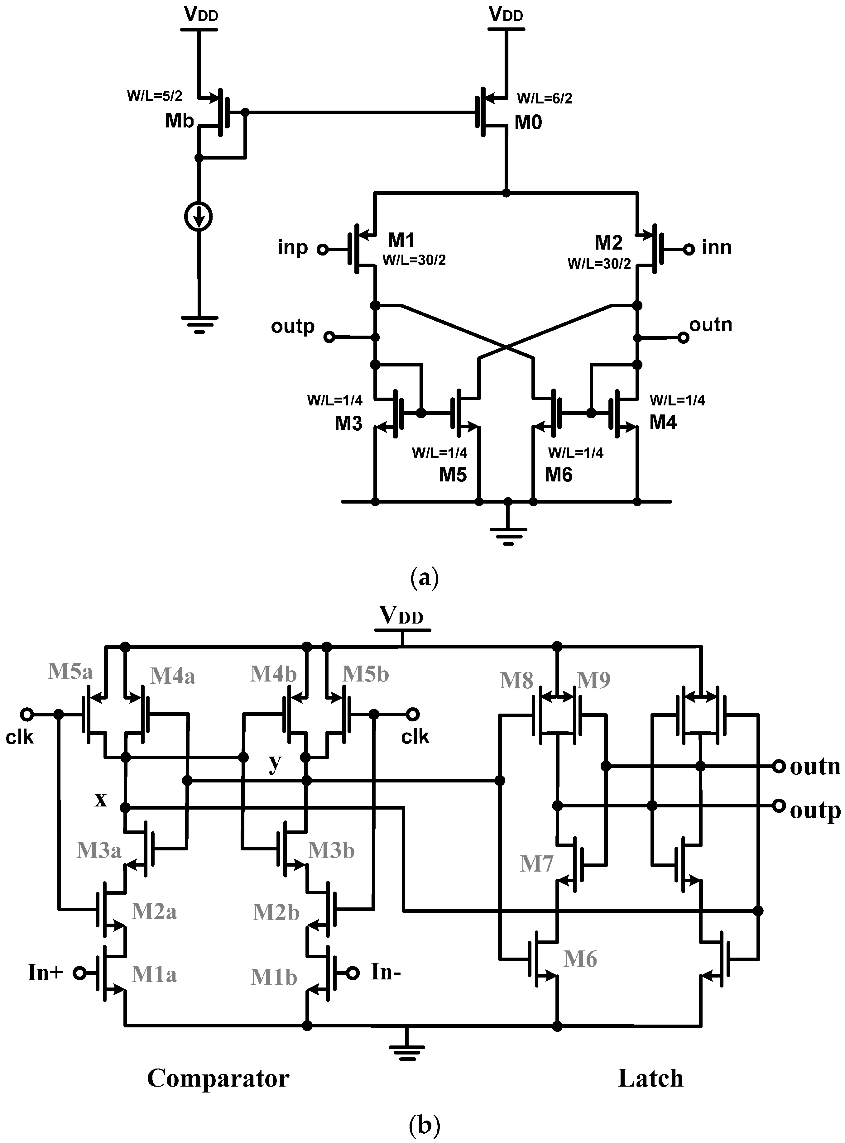
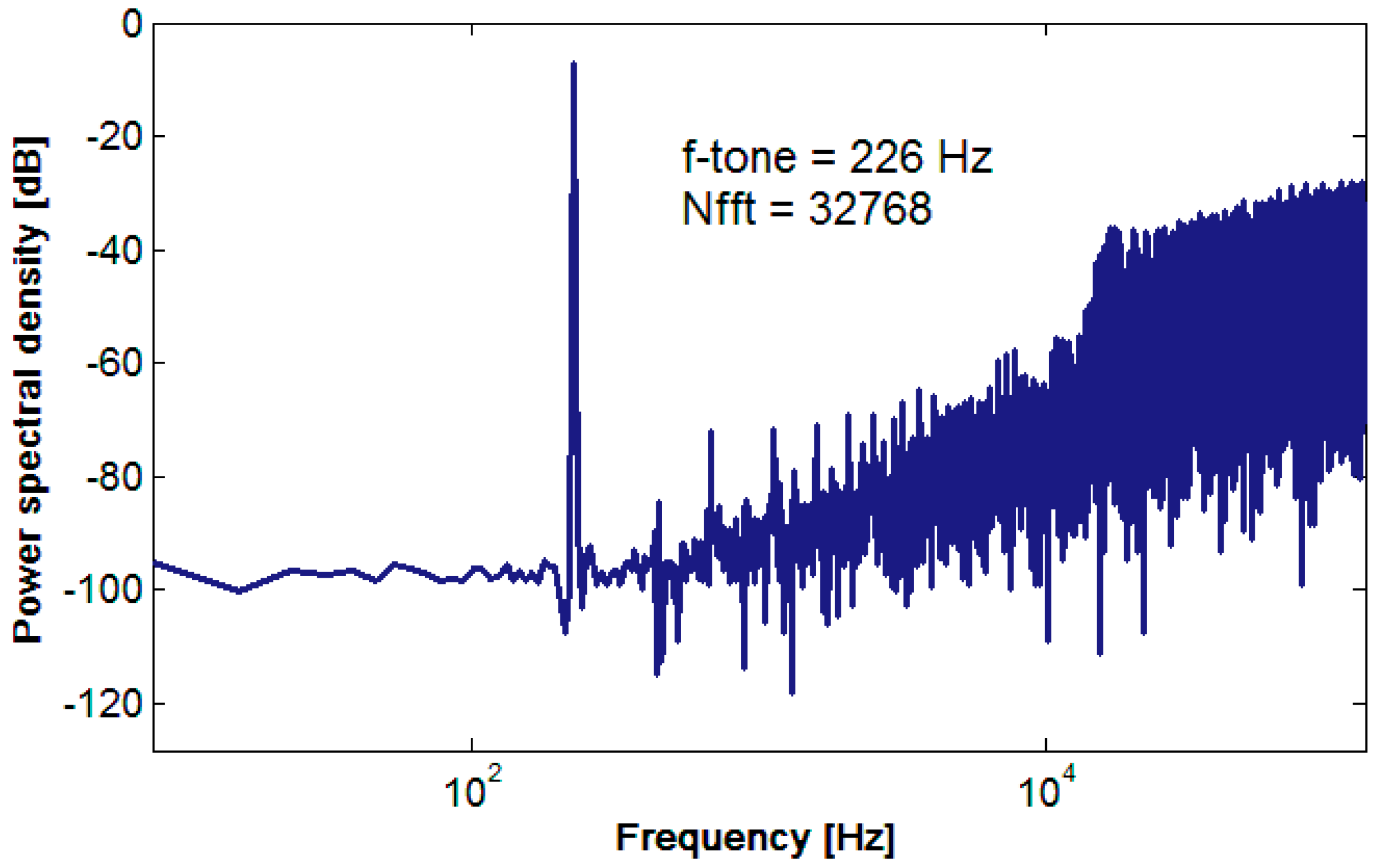
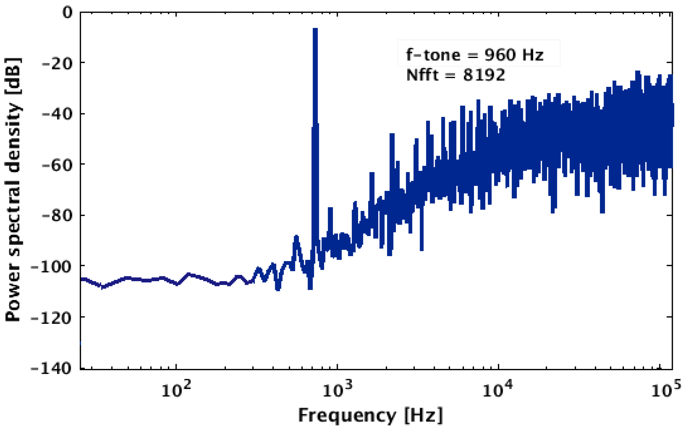
The single-bit quantizer is inherently linear. A multi-bit quantizer is not preferable for the low power and moderate resolution in this application, because the internal DAC becomes nonlinear, requiring dynamic element matching (DEM) or other complementary techniques for DAC linearization, which increase the hardware complexity and, thus, the total power consumption.

4. Modulator Circuit Design and Building Blocks

In this section, the details of modulator circuit design and its building blocks are discussed.

4.1. Modulator Circuit

Figure 4 shows the schematic of the designed second-order SC ΔΣ modulator using the proposed pseudo-differential integrators. The SC CMFB circuit is not shown and is omitted for simplicity. The proposed inverter-based amplifier in feedback configuration does not provide a virtual ground at the integrator input, because it has only one input terminal (Figure 1c). Combined with the CDS technique to cancel out the input offset and to attenuate the 1/f noise [16], two instances of the designed inverter-based amplifier are used to realize a pseudo-differential integrator with a virtual ground. There is a half-cycle delay between the integrators, i.e., when the first integrator samples the input onto CS1 and the offset of the inverter onto CC1, the second integrator is in charge transfer phase and vice versa. Since all feedforward paths have to create full delay paths according to Figure 3a, a half-cycle delay element is inserted in the internal feedforward path using SC implementation.
The summation of the feedforward paths is realized by the parallel capacitor branches at the quantizer input by using an SC passive network. The feedforward architecture is preferable due to its relaxed OTA’s performance requirements and low internal swings.

4.2. Low-Voltage Clocking and Clock-Boosting Circuitries

Figure 5 shows the non-overlapping clock generation circuitry used to provide the clock timing required by the modulator. The entire circuit employs low-VTH low-power (LVTLP) devices enabling operation at 300 mV. The transistor aspect ratios of the CMOS inverters and the output buffers are specified in µm/µm in the figure. The aspect ratios of the CMOS NAND gate for PMOS and NMOS devices are 0.24 µm/1.5 µm and 0.135 µm/1.5 µm, respectively. In order to open and close the switches properly, they are implemented as transmission gates with low-VTH transistors, driven by an ultra-low-voltage charge-pump clock doubler [13].
Figure 6 shows the schematic of the clock boosting circuit, which is composed of a charge-pump voltage doubler with two cross-coupled NMOS devices, two capacitors as large as 5 pF and two inverters as the buffer and level shifter. Low-VTH devices were employed in the charge-pump circuit and level shifters for low voltage operation at 300 mV. The Ф1L and Ф2L are two non-overlapping clocks generated by the circuit in Figure 5 with a voltage level equal to 0.3 V, whereas Ф1H and Ф2H are level shifted up to 0.6 V. Hereafter, for simplicity, we denote Ф1H and Ф2H as Ф1 and Ф2, as in Figure 4. In a similar way, the Ф1d and Ф2d are generated and level shifted.

4.3. Ultra-Low-Voltage Sub-Threshold Quantizer

The single-bit quantizer is implemented using a dynamic comparator preceded by a single-stage preamplifier, as shown in Figure 7. Table 2 summarizes the transistors dimension in µm. At a 0.3 V supply, the regular preamplifier and comparator circuits do not function properly in the strong inversion.
The input signals have a common-mode level equal to 0.15 V (i.e., VDD/2), which is not adequate to turn on the input transistors. The threshold voltage of the used low-VTH transistors in this technology itself is more than 0.15 V. On the other hand, stacking more than three transistors is impractical. Therefore, the single-bit quantizer (including the preamplifier circuit and the dynamic comparator and latch) is designed in the deep sub-threshold regime, providing very high power efficiency. The entire circuit dissipates only 6 nW, while clocked at 256 kHz. The quantizer operating at 0.3 V ± 10% was simulated against process, voltage and temperature (PVT) variations. It is capable of detecting an input signal as low as 200 µV, whereas the modulator’s least significant bit (LSB) is 300 µV for a full-scale reference voltage of 300 mV and 10 bit resolution.
The gain of the preamplifier degrades to 5 dB at a 0.3 V supply. Thus, it employs a gain-enhanced positive feedback in order to boost the low-frequency gain [2]. The preamplifier exploits low-VTH transistors, providing more headroom for ultra-low voltage operation. For robust function against PVT variations, the effect of mismatch and process variations over DC gain was simulated using Monte Carlo analysis. Figure 8a shows the histogram of the DC gain for 5000 runs, which demonstrates the mean value of 10.55 dB. The frequency response was also simulated for 1000 runs, as depicted in Figure 8b. The worst-case DC gain in this plot is more than 9 dB.

5. Simulation Results

The proposed 0.3 V delta-sigma modulator was designed and simulated in a 65 nm CMOS process. Figure 9 shows the output power spectrum for a −2 dB full-scale (dBFS), 226 Hz sine-wave input. Figure 10 shows the power spectrum for a 960 Hz input, near the signal bandwidth edge, with a full scale input amplitude (i.e., 0 dBFS). The differential input signal range is 500 mVpp. The modulator performance is simulated against process corners and 10% supply voltage variations, the achieved worst-case peak SNR and SNDR are 64.4 dB and 60.7 dB, respectively, within a 1.0 kHz signal bandwidth with a 256 kHz sampling clock frequency. The total power consumption from a 0.3 V power supply is 0.85 μW, in which the digital power is only 9%, including clock generation and clock boosting circuitries. Figure 11 presents the modulator SNDR versus the input differential amplitude in dBFS. The performance metrics are summarized in Table 3. The resulting figure of merit (FOM) is 0.46 pJ/conversion-step, by calculating FOM = power/(2ENOB × 2 × bandwidth) with ENOB as the effective number of bits. The modulator can work up to a 0.5 V power supply.

6. Comparison of the Power Efficiency

The performance of the presented modulator in Section 4 and Section 5 is compared to previous state-of-the-art low-voltage modulators in Table 4. Two commonly-used FOMs are employed, which are defined below:
F O M 1 = P o w e r 2 ( S N D R 1.76 ) / 6.02 × 2 × B W
F O M 2 = D R d B + 10 log ( B W P o w e r )
The FOM1 favors high-resolution ADCs, whereas the FOM2 favors high-DR ADCs. These FOM definitions disregard VDD, the threshold voltage of the corresponding technology, and the available swing. According to the FOM definitions given above, the designed inverter-based, second-order modulator achieves 0.46 pJ/conversion-step and 156 dB, respectively, which are comparable to the other state-of-the-art modulators operating with supply voltages below 0.4 V. Among others, the passive modulator in [
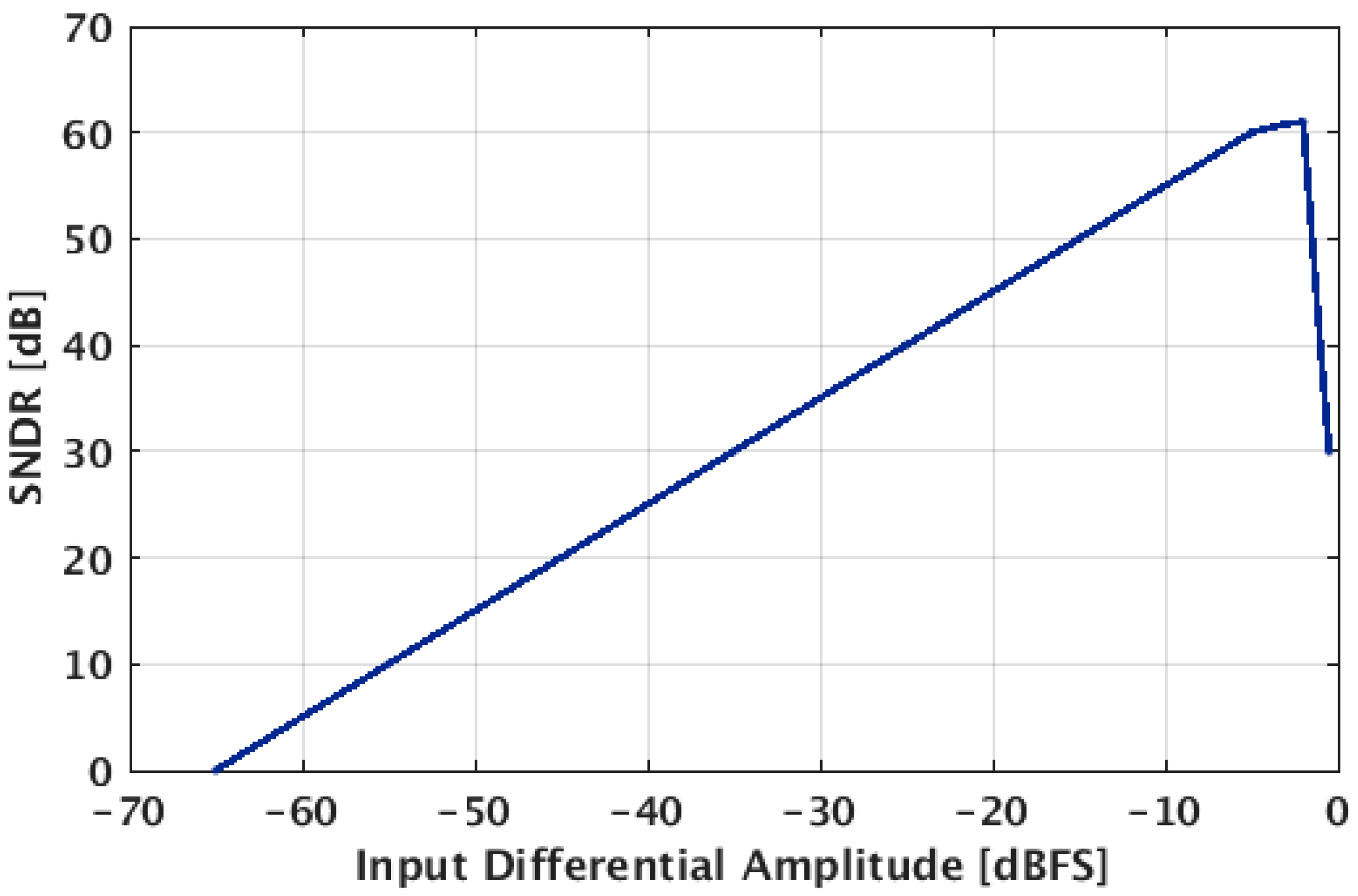
2] operating at a 0.5 V supply consumes the lowest power (only 250 nW) while gaining moderate resolution (65 dB SNDR) and 72 dB DR. It looks attractive when using both FOM definitions given by Equations (12) and (13).
The modulator design in the ultra-low voltage domain (below 0.5 V) is becoming more and more challenging due to the limited available signal swing and switch overdrive voltage. The output swing of an OTA directly determines the integrators’ swing, which indeed defines the modulator reference voltage. As a consequence, the maximum input signal, Vin.max, that determines the DR of the ADC at a given input-referred noise floor Pn is limited by the reference voltage or the integrators’ swing. The DR can be derived as:
D R = 10 log V i n . max 2 / 2 P n + P D
where PD is the input-referred distortion. To maintain the same DR in lower supply voltages, the noise floor and distortion power have to be decreased, requiring higher power consumption [21]. Generally speaking, for a better power efficiency, it is not desirable to reduce the supply voltage, because the analog power increases. However, specific applications, such as body implants (e.g., cardiac pacemakers, cochlear implants, etc.), demand ultra-low-voltage operation in the order of human body potentials.
It should be noted that the threshold voltage does not scale at the same proportion as the supply voltage, which limits the available overdrive voltage of the operating switches in SC designs. For fair comparisons of the modulators listed in Table 4, in addition to the commonly-used FOM1 and FOM2, the proposed FOM3 takes into account the VDD, as well.
F O M 3 = P o w e r × V D D 2 ( S N D R 1.76 ) / 6.02 × 2 × B W
In fact, the most effective comparison among different modulators is when we consider the threshold voltage in addition to the supply voltage, VDD, because the available voltage headroom for analog blocks and the overdrive voltage for the switching transistors (i.e., VGSVTH) depend directly on VTH. Therefore, for a fair comparison, we need to consider the term VDDVTH in the numerator of the FOM3 given by Equation (15), rather than merely VDD. For simplicity, we assume all technologies used in Table 4 have the same VTH. According to FOM3 and considering operating VDD, the proposed modulator achieves a competitive figure of merit of 0.139 pJ.V/conversion-step.

7. Conclusions

An ultra-low-voltage, energy-efficient ΔΣ modulator is introduced in this paper for medical implant devices. In the absence of cascoding, a new gain-enhanced inverter-based amplifier was proposed to compensate for the reduced inverter’s DC gain and GBW. To overcome the switches’ overdrive limitation, the charge pump clock doublers were used to boost the clock signals’ level. The single-bit quantizer, including the preamplifier, dynamic comparator and latch, was designed in the deep sub-threshold regime, providing very high power efficiency. The entire modulator operates reliably against PVT variations from a 300 mV ± 10% supply voltage. The modulator design is compatible with human body potentials, as well as the energy efficiency intended for the target applications.

Acknowledgments

The author would like to thank Gabor C. Temes of Oregon State University for his valuable guidelines, recommendations and proofreading. He also would like to thank Atila Alvandpour of Linköping University for the project support.

Author Contributions

In this research work, the author Ali Fazli Yeknami contributed to the literature search and came up with the idea of the new gain-enhanced inverter-based amplifier technique that can reliably work at supply voltages near 300 mV. He was responsible for simulating the entire delta-sigma modulator against PVT variations, for a comprehensive comparison with other ultra-low voltage designs. The manuscript was written by Ali Fazli Yeknami and proofread for the technical writing and formatting aspects by Gabor C. Temes of Oregon State University. The author also had extensive discussions with Atila Alvandpour at Linköping University from the standpoint of the project specifications and biomedical design requirements.

Conflicts of Interest

The author declares no conflict of interest.

References

  1. Muller, R.; Gambini, S.; Rabaey, J.M. A 0.013 mm2 5 μW DC-coupled neural signal acquisition IC with 0.5 V supply. IEEE J. Solid-State Circuits 2012, 47, 232–243. [Google Scholar] [CrossRef]
  2. Yeknami, A.F.; Alvandpour, A. A 0.5-V 250-nW 65-dB SNDR Passive ΔΣ Modulator for Medical Implant Devices. In Proceedings of 2013 IEEE International Symposium on Circuits and Systems (ISCAS), Beijing, China, 19–23 May 2013; pp. 2010–2013.
  3. Gerosa, A.; Neviani, A. A 1.8 µW sigma-delta modulator for 8-bit digitization of cardiac signals in implantable pacemakers operating down to 1.8 V. IEEE Trans. Circuits Syst. II Express Briefs 2005, 52, 71–76. [Google Scholar] [CrossRef]
  4. Zou, X.; Xu, X.; Yao, L.; Lian, Y. A 1-V 450-nW Fully Integrated Programmable Biomedical Sensor Interface Chip. IEEE J. Solid-State Circuits 2009, 44, 1067–1077. [Google Scholar] [CrossRef]
  5. Lu, T.-C.; Van, L.-D.; Lin, C.-S.; Huang, C.-M. A 0.5 V 1 KS/s 2.5 nW 8.52-ENOB 6.8 fJ/Conversion-Step SAR ADC for Biomedical Applications. In Proceedings of IEEE Custom Integrated Circuits Conference (CICC), San Jose, SC, USA, 19–21 September 2011; pp. 1–4.
  6. Yeknami, A.F.; Alvandpour, A. Low-Power Low-Voltage ΔΣ Modulator Using Switched-Capacitor Passive Filter. In VLSI-SOC: At the Crossroads of Emerging Trends; Orailoglu, A., Ugurdag, H.F., Sliveira, L.M., Margala, M., Reis, R., Eds.; Springer: Dordrecht, The Netherlands, 2015; Volume 461, pp. 94–118. [Google Scholar]
  7. Yeknami, A.F.; Alvandpour, A. A 0.7-V 400-nW Fourth-Order Active-Passive Delta-Sigma Modulator with One Active Stage. In Proceedings of 21st IEEE International Conference on Very Large Scale Integration (VLSI-SoC), Istanbul, Turkey, 7–9 October 2013; pp. 1–6.
  8. Yeknami, A.F.; Alvandpour, A. A 2.1 μW 80 dB SNR DT ΔΣ modulator for medical implant devices in 65 nm CMOS. J. Analog Integr. Circuits Signal Proc. 2013, 77, 69–78. [Google Scholar] [CrossRef]
  9. De Melo, J.L.; Querido, F.; Paulino, N.; Goes, J. A 0.4-V 410-nW Opamp-Less Continuous-Time Σ∆ Modulator for Biomedical Applications. In Proceedings of 2014 IEEE International Symposium on Circuits and Systems (ISCAS), Melbourne, Australia, 1–5 June 2014; pp. 1340–1343.
  10. Roh, H.; Lee, H.; Choi, Y. A 0.8-V 816-nW delta-sigma modulator for low-power biomedical applications. J. Analog Integr. Circuits Signal Proc. 2010, 63, 101–106. [Google Scholar] [CrossRef]
  11. Yeknami, A.F.; Qazi, F.; Alvandpour, A. Low-power DT ΔΣ modulators using SC passive filters in 65 nm CMOS. IEEE Trans. Circuits Syst. I 2014, 61, 358–370. [Google Scholar] [CrossRef]
  12. Chae, Y.; Han, G. Low voltage, low power, inverter-based switched-capacitor delta-sigma modulator. IEEE J. Solid-State Circuits 2009, 44, 458–472. [Google Scholar] [CrossRef]
  13. Pan, F.; Samaddar, T. Charge Pump Circuit Design, 1st ed.; McGraw-Hill Electronic Engineering Series; McGraw-Hill: New York, NY, USA, 2006. [Google Scholar]
  14. Pun, K.P.; Chatterjee, S.; Kinget, P.R. A 0.5 V 74-dB SNDR 25-kHz continuous-time delta-sigma modulator with a return-to-open DAC. IEEE J. Solid-State Circuits 2007, 42, 496–507. [Google Scholar] [CrossRef]
  15. Michel, F.; Steyaert, M. A 250 mV 7.5 µW 61 dB SNDR SC ΔΣ modulator using near-threshold-voltage-biased inverter amplifiers in 130 nm CMOS. IEEE J. Solid-State Circuits 2012, 47, 709–721. [Google Scholar] [CrossRef]
  16. Enz, C.C.; Temes, G.C. Circuit techniques for reducing the effects of op-amp imperfections: autozeroing, correlated double sampling, and chopper stabilization. Proc. IEEE 1996, 84, 1584–1614. [Google Scholar] [CrossRef]
  17. Yao, L.; Steyaert, M.; Sansen, W. Low-Power Low-Voltage Sigma-Delta Modulators in Nanometer CMOS; Springer: Dordrecht, The Netherlands, 2006. [Google Scholar]
  18. Wismar, U.; Wisland, D.; Andreani, P. A 0.2 V, 7.5 µW, 20 kHz ΣΔ Modulator with 69 dB SNR in 90 nm CMOS. In Proceedings of 33rd European Solid State Circuits Conference (ESSCIRC), Munich, Germany, 11–13 September 2007; pp. 206–209.
  19. Qiao, Z.; Zhou, X.; Li, Q. A 250 mV 77 dB DR 10 kHz BW SC ΔΣ Modulator Exploiting Sub Threshold OTAs. In Proceedings of 40th European Solid State Circuits Conference (ESSCIRC), Venice, Italy, 22–26 September 2014; pp. 419–422.
  20. Yoon, Y.; Roh, H.; Roh, J. A True 0.4-V Delta-Sigma Modulator Using a Mixed DDA Integrator Without Clock Boosted Switches. IEEE Trans. Circuits Syst. II Express Briefs 2014, 61, 229–233. [Google Scholar] [CrossRef]
  21. Yeknami, A.F. Low-Power Delta-Sigma Modulators for Medical Applications. Ph.D. Thesis, Linköping University, Linköping, Sweden, 21 January 2014. [Google Scholar]
Figure 1. Schematic of the inverter amplifiers: (a) conventional CMOS inverter with biasing; (b) cascode inverter; (c) inverter-based current-mirror operational transconductance amplifier (OTA) using an input inverter stage and a current mirror output stage; single-ended is shown; (d) parasitic capacitance at internal node.
Jlpea 06 00004 g001
Figure 2. (a) DC gain and (b) gain-bandwidth (GBW) variations versus supply voltage for the CMOS inverter shown in Figure 1a and the proposed gain-enhanced, inverter-based amplifier shown in Figure 1c; (c) the zoomed version of the Figure 2b for clarity.
Jlpea 06 00004 g002aJlpea 06 00004 g002b
Figure 3. (a) The scaled modulator input-feedforward architecture using a second-order loop filter and a single-bit quantizer. Integrators with half-cycle delay were used to adopt the built-in correlated double-sampling (CDS) scheme for offset cancellation and 1/f noise attenuation; (b) the magnitude of the noise transfer function (NTF) and signal transfer function (STF) of the modulator with respect to the normalized frequency.
Jlpea 06 00004 g003
Figure 4. Schematic diagram of the one-bit second-order switched-capacitor (SC) delta-sigma modulator using pseudo-differential integrators. Each integrator circuit shown in red represents the proposed inverter-based current mirror amplifier discussed in Section 2. VH and VL denote the positive and negative reference voltages. CM, common mode.
Jlpea 06 00004 g004
Figure 5. Clock generation circuitry using low-VTH low-power (LVTLP) devices. The transistor aspect ratios of the inverters and the output buffers are given in µm/µm. This provides two non-overlapping clocks (Ф1L, Ф2L) and their delays (Ф1dL, Ф2dL) to avoid signal-dependent charge injection.
Jlpea 06 00004 g005
Figure 6. Clock doubler with a charge-pump circuit and level shifters using low-VTH devices. The transistor aspect ratios are specified in µm/µm.
Jlpea 06 00004 g006
Figure 7. (a) Low-voltage differential gain-enhanced preamplifier circuit operating in the sub-threshold regime. The transistors aspect ratios are specified in µm/µm. (b) Low-voltage dynamic comparator and latch designed in the sub-threshold regime. The transistors aspect ratios are summarized in Table 2.
Jlpea 06 00004 g007
Figure 8. (a) Histogram of the DC gain of the low-voltage preamplifier shown in Figure 7a operating in the sub-threshold regime from the Monte Carlo simulations; (b) Bode plot of the frequency response from Monte Carlo simulations.
Jlpea 06 00004 g008
Figure 9. Simulated output power spectrum of the designed modulator for the input signal frequency of 226 Hz with a −2 dBFS amplitude.
Jlpea 06 00004 g009
Figure 10. Simulated output power spectrum of the designed modulator for the input signal frequency of 960 Hz and a full-scale amplitude (0 dBFS). The effective signal bandwidth is 1 kHz.
Jlpea 06 00004 g010
Figure 11. Simulated signal-to-noise and distortion ratio (SNDR) versus input differential amplitude in dBFS.
Jlpea 06 00004 g011
Table 1. Transistor aspect ratios and bias setting for the gain-enhanced current mirror inverter amplifier in a 65 nm CMOS.
TransistorW/L (µm/µm)
M11/0.8
M29/0.8
M32/0.2
M416/0.2
M55/0.25
CapacitorValue (pF)
Cbn = Cbp0.5
CLoad3.0
Table 2. Transistor aspect ratios of the clocked comparator and latch designed in the sub-threshold regime.
Transistors in ComparatorW/L (µm/µm)
M1a/M1b8/0.18
M2a/M2b4/0.18
M3a/M3b3/0.18
M4a/M4b25/0.18
M5a/M5b30/0.18
Transistors in LatchW/L (µm/µm)
M61/0.18
M70.5/0.18
M81/0.18
M91/0.18
Table 3. Simulated performance results.
MetricsSimulated Value
Supply voltage0.3 V
Technology65 nm CMOS
Clock frequency256 kHz
Signal bandwidth1 kHz
Differential input range0.5 Vpeak-to-peak
Temperature range0 to 100 °C
Peak SNRslow corner 64.4 dB
typical corner 65.5 dB
fast corner 67 dB
Peak SNDRslow corner 60.7 dB
typical corner 62 dB
fast corner 63.2 dB
Dynamic range65 dB
Power consumption0.85 µW
Table 4. Performance comparison with previously-reported low-voltage low-power delta-sigma modulators. FOM, figure of merit.
Parameters[15][18][19][9] [20]This Work
VDD (V)0.250.20.30.40.40.3
Bandwidth (Hz)10 k20 k20 k10 k20 k1 k
Power consumption (µW)7.57.579.30.411400.85
Sampling frequency (Hz)1.4 M12 M2.56 M2 M3.2 M256 k
SNDR (dB)6160.374586860.7
DR (dB)6468.977647465
Technology (nm)1309013013013065
FOM1 (pJ/step)0.4770.2220.4810.0321.70.464
FOM2 (dB)155163161168155.5156
FOM3 (pJ.V/step)0.1190.0440.1440.0130.680.139
Results from simulation. Other references provide experimental results.

