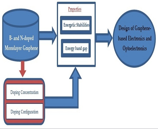
1. Introduction
Graphene, a single atomic layer of graphite which exhibits exceptional structural, mechanical, electrical, optical, and chemical properties, has applications in numerous fields [
1]. Graphene has attracted the attention of researchers from both experimental and theoretical points of view after its successful isolation in 2004 [
2], especially for electronics owing to its exceptional properties [
3] such as ballistic electron transport at room temperature [
4], high charge carrier mobility [
5], room-temperature fractional quantum Hall effect [
6], and finite electrical conductivity at zero charge carrier density [
7]. These features of graphene that make it a potential candidate for future nanoelectronics [
8,
9] arise from its unique zero energy band gap with linear energy-momentum relation around the Dirac point [
10,
11]. However, the absence of a band gap in graphene limits its applications in various nanoelectronic devices, such as
p-
n junction diodes and transistors, and in other energy-related devices such as supercapacitors, solar cells, and fuel cells.
In order to exploit the potential of graphene for electronics, a sizeable band gap should open up in graphene. Until now, various approaches such as application of an external electric field [
12], chemical functionalization [
13], use of graphene nanoribbons [
14], and doping with heteroatoms [
15] have been proposed for opening a band gap in graphene. Among these, substitutional doping is suggested to be the most effective method for modifying the electronic properties of graphene, due to the strong dependency of the material properties on the structure. Doping of graphene with other elements would not result in significant degradation of other favorable features of graphene that makes it suitable for enabling nano-sized electronics. The introduction of dopants into the graphene lattice could also lead to important modifications of physical and chemical properties that could be tailored for developing various graphene-based devices with applications in sensing [
16,
17,
18,
19,
20,
21,
22], energy storage [
23,
24,
25,
26], gas storage [
27,
28,
29], etc. Among various dopant atoms, boron (B) and nitrogen (N) atoms have gained significant research attention being the nearest neighbors to carbon (C) that provide a strong probability of entering the graphene lattice and due to the electron acceptor and donor nature of B and N atoms that produces
p-type and
n-type graphene, respectively [
30,
31,
32,
33]. The
p-type and
n-type graphene sheets produced by B- and N-doping could be employed for the fabrication of complementary devices in future graphene-based electronic circuits.
There have been many reports on band gap engineering of graphene using substitutional doping [
15,
30,
34,
35,
36,
37,
38,
39,
40,
41,
42,
43,
44,
45,
46,
47]. For instance, Wu et al. [
37] investigated the geometry, electronic structure, and magnetic properties of graphene doped with light non-metallic atoms such as B, N, O, and F. An ab initio study on the band gap opening in graphene by single B- and N-atom doping in 8, 18, 32, and 50 host C atoms has also been reported [
42]. All these works on doped graphene systems have shown that dopant atoms modify the electronic band structure of graphene by introducing an energy gap so that the behavior of graphene changes from semi-metallic to semiconducting. However, one B- and N-atom doping in 3N × 3N (where N is an integer) graphene supercells have shown zero band gap at the Dirac point [
38,
42,
44], whereas, in the case of the one B- and N-atom doping in the (3N − 1) × (3N − 1) and (3N + 1) × (3N + 1) supercells of pristine graphene, there is a band gap which can be tunable by the doping concentration. Zhou et al. [
44] discovered an interesting 3N rule for periodically doped graphene sheets, which suggests that when the primitive cell is 3N × 3N, the doped graphene has a zero gap or negligible gap, and the properties of doped graphene can be predicted by their primitive cell sizes.
The effect of doping graphene with B and N concentrations varying from 2% to 12% (simulated by varying the number of dopants from one to six in 50 host atoms) on the geometry and electronic structure of single-layer graphene has been systematically analyzed by Rani and Jindal [
30]. They observed a dependence of the band gap not only on the concentration of dopants, but also on the position of the dopant atom in the graphene sheet. The results showed a maximum band gap upon placing the dopants at the same sublattice locations and a minimum band gap upon placing the dopants at alternate sublattice locations of the graphene. Another study presented the electronic and magnetic properties of single-layer graphene doped with N atoms and analyzed the dependence of magnetic moments and band gaps in graphene on N-substitutional doping configurations by considering two N atoms in graphene supercells containing 8, 18, and 32 host C atoms [
43].
A systematic analysis of the structural and electronic properties of N-doped graphene with two N-substitutional dopants in 3N × 3N graphene supercells by considering different doping configurations has not been reported. To the best of our knowledge, a similar study on B-doped graphene with more than one dopant in 3N × 3N graphene supercells has also still not appeared in the literature. In this paper, we investigate the atomic structures, the stabilities, and the electronic properties—specifically the band structures of graphene doped with B and N atoms in 8, 18, 32 and 72 host C atoms. As B and N atoms can be placed at C sites of the crystal lattice in many different configurations, several substitutional dopant sites in the graphene sheet are analyzed. The effect of B- and N-doping on the structural and electronic properties of graphene is analyzed by varying the doping concentrations from 1.39% to 25% and by considering different configurations for the same doping concentration. The dependence of the cohesive energy per atom on the doping concentration and the different doping configurations are also studied to understand the stabilities and to compare the energetics of the B- and N-doped systems. Fourteen doping concentrations between 1.39% and 25% are considered for the study.
2. Computational Method
All calculations are performed within the framework of density functional theory (DFT) as implemented in ABINIT code [
48]. The generalized gradient approximation (GGA) exchange-correlation (XC) functional in the Perdew–Burke–Ernzerhof (PBE) form [
49] is adopted in the structural optimization and electronic structure calculations of both pristine graphene and different doped graphenes. Norm-conserving Troullier–Martins type pseudopotentials [
50] are used to describe the electron–ion interactions. The energy convergence criterion is chosen to be ~10 meV/atom. A plane-wave basis set with converged cutoff energy of 816 eV is used (see
Supplementary Figure S1). The sampling of the Brillouin zone is performed using the k-point mesh generated by the Monkhorst–Pack scheme [
51]. Converged k-point grids corresponding to a 24 × 24 × 1 grid for a graphene unit cell are used for different graphene supercells (see
Supplementary Figure S2). For all systems, the relaxation of basis vectors and atomic coordinates are performed by minimizing the total energy. Structural optimization has been conducted using the Broyden–Fletcher–Goldfard–Shanno (BFGS) minimization until the residual forces on atoms are lower than 0.0025 eV/Å.
A single-layer graphene sheet is modeled using four different supercell sizes, i.e., a 2 × 2 ((3N − 1) × (3N − 1), where N = 1) supercell with 8 C atoms, a 3 × 3 (3N × 3N, where N = 1) supercell with 18 C atoms, a 4 × 4 ((3N + 1) × (3N + 1), where N = 1) supercell with 32 C atoms, and a 6 × 6 (3N × 3N, where N = 2) supercell with 72 C atoms, where the distance between the adjacent graphene layers along the perpendicular direction is taken as 10 Å to avoid interlayer interactions due to periodic boundary conditions. B- and N-doped graphenes are simulated by replacing the C atom in the supercell structure by a B or N atom and by choosing the corresponding pseudopotentials. B- and N-doping concentrations from 1.39% to 25% are modeled through the substitution of one and two C atoms in the 2 × 2 supercell by dopant atoms, which corresponds to 12.5% and 25% doping concentrations, respectively; the substitution of one, two, three, and four C atoms in the 3 × 3 supercell by dopant atoms, which corresponds to 5.56% 11.11%, 16.67%, and 22.22% doping concentrations, respectively; the substitution of one and two C atoms in the 6 × 6 supercell by dopant atoms, which corresponds to 1.39% and 2.78% doping concentrations, respectively; the substitution of one, two, three, four, five, and six C atoms in the 4 × 4 supercell by dopant atoms, which corresponds to 3.13%, 6.25%, 9.38%, 12.5%, 15.63%, and 18.75% doping concentrations, respectively.
In all cases, we first optimize the geometry of the B- and N-doped systems. The cohesive energy per atom,
, is calculated as [
30]
where
and
represent the total energies of the considered doped system and of the individual elements present within the doped system. The total energies of the individual elements (C, B, or N) are calculated by defining a large supercell and adding the element (C, B, or N) at (0, 0, 0).
is the total number of atoms present in the system, and
ni is the total number of species
i present in the configuration. The values of
indicate the energetic stability of the systems. The lesser the value, the more stable the system is. Finally, the electronic band structures are computed for the optimized doped systems from which the widths of the band gap are determined. We elucidate the dependence of the band gap and the cohesive energy per atom on the concentration and position of the dopant atoms.
3. Results
3.1. Pristine Graphene
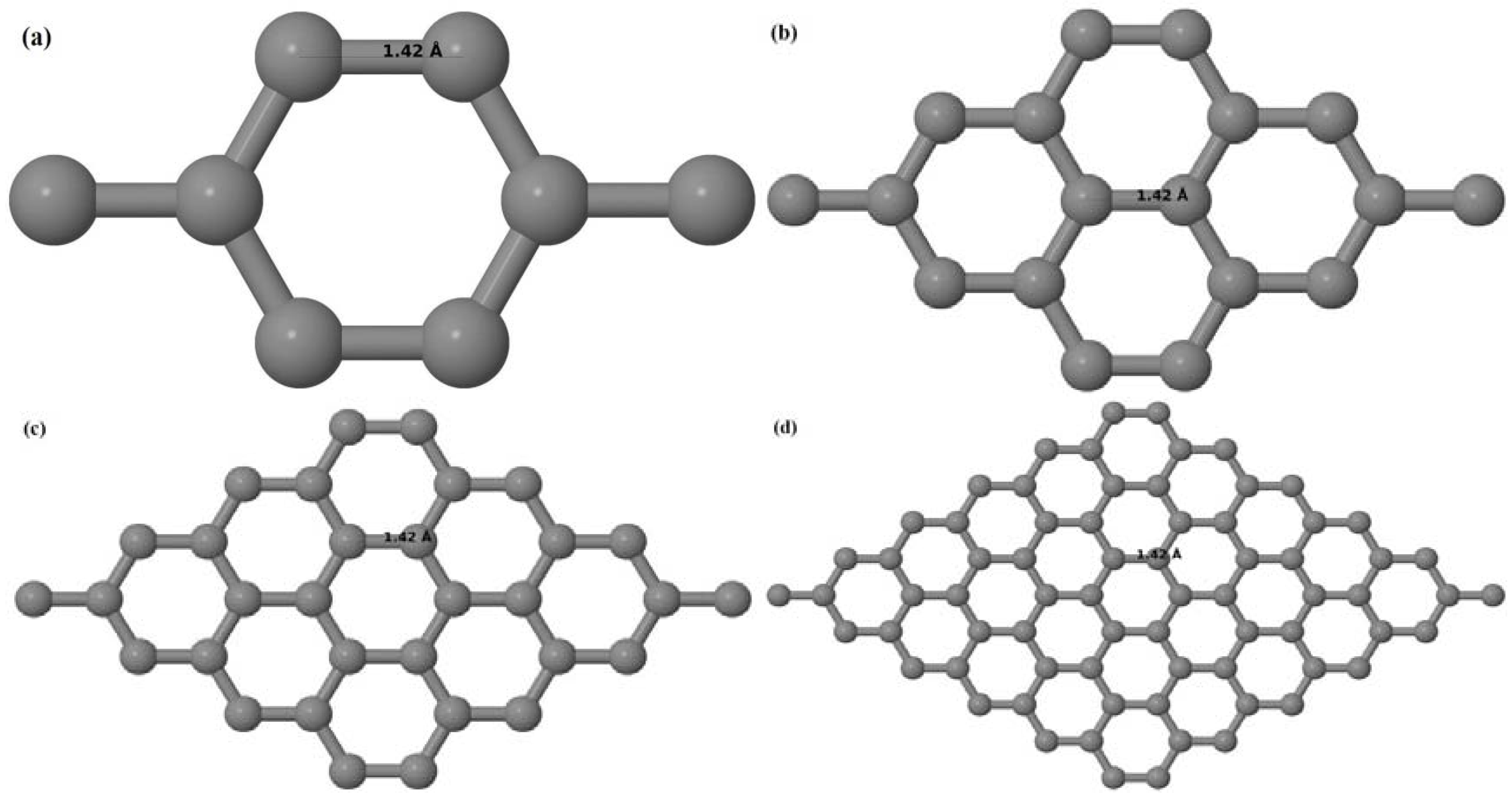
Upon structural optimization of pristine graphene (PG), the lattice constant and the C–C bond length were observed to be 2.458 Å and 1.42 Å. The calculated lattice constant is in good agreement with the experimental value of 2.46 Å [
52], and the calculated C–C bond length of 1.42 Å as seen in
Figure 1a–d is very close to the experimental value of 1.421 Å [
3,
52]. The relaxed geometries and band structures of 2 × 2, 3 × 3, 4 × 4, and 6 × 6 graphene supercells obtained from the calculations are shown in
Figure 1a–d and
Figure 2a–d, respectively.
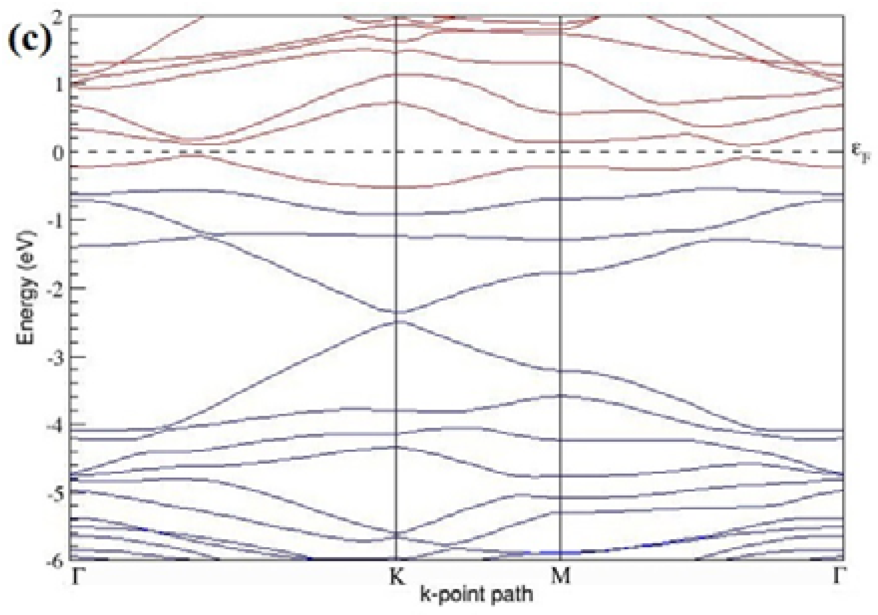
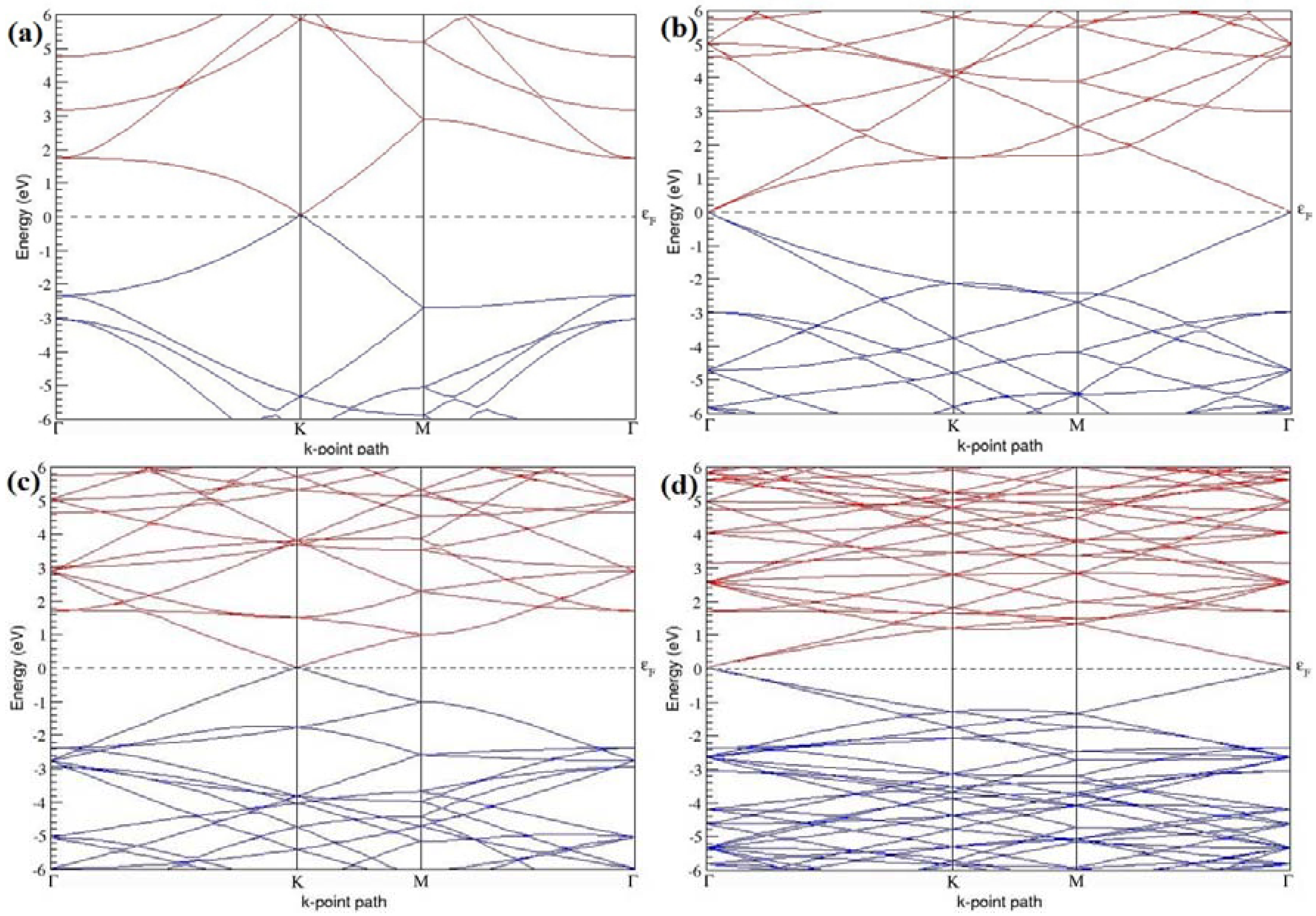
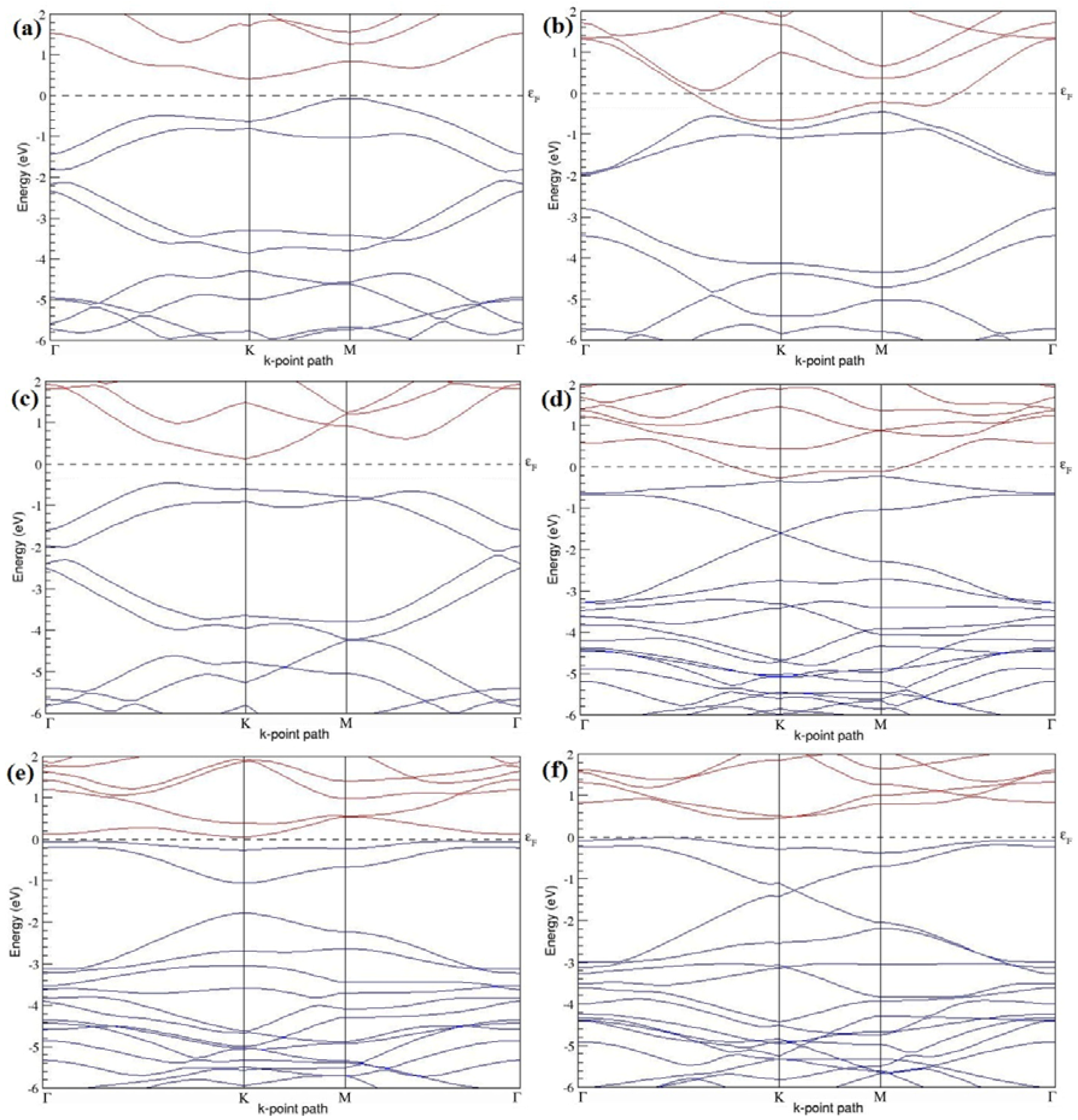
The band structures of the PG sheets (
Figure 2a–d) along the high symmetry points (Γ-K-M-Γ) of the hexagonal Brillouin zone of graphene, which exhibit zero energy band gap and linear in-plane dispersion around the Fermi level, are found to be in good agreement with the reported literature [
7], which presents the reliability of the employed calculation method. In the band structures of 2 × 2 and 4 × 4 graphene supercells, the top of the valence band and the bottom of the conduction band degenerate at the K-point as seen in
Figure 2a,c, whereas, in 3 × 3 and 6 × 6 supercells, the degeneracy is observed at the Γ-point, as presented in
Figure 2b,d. This is in accordance with the previous reports that the Dirac point moves into the Γ-point, when the supercells are dimensions of three (3 × 3, 6 × 6, 9 × 9 supercells, etc.) [
44].
After successful reproduction of the structural and the electronic band structures of PG, PG is doped with 14 different concentrations of B and N atoms. The study of the change in the geometries and the electronic structures of graphene upon doping with varying B- and N-atom concentrations and the analysis of the band gap for each doping concentration and for different dopant sites for the same doping concentration are carried out as described below.
3.2. B-Doped Graphene
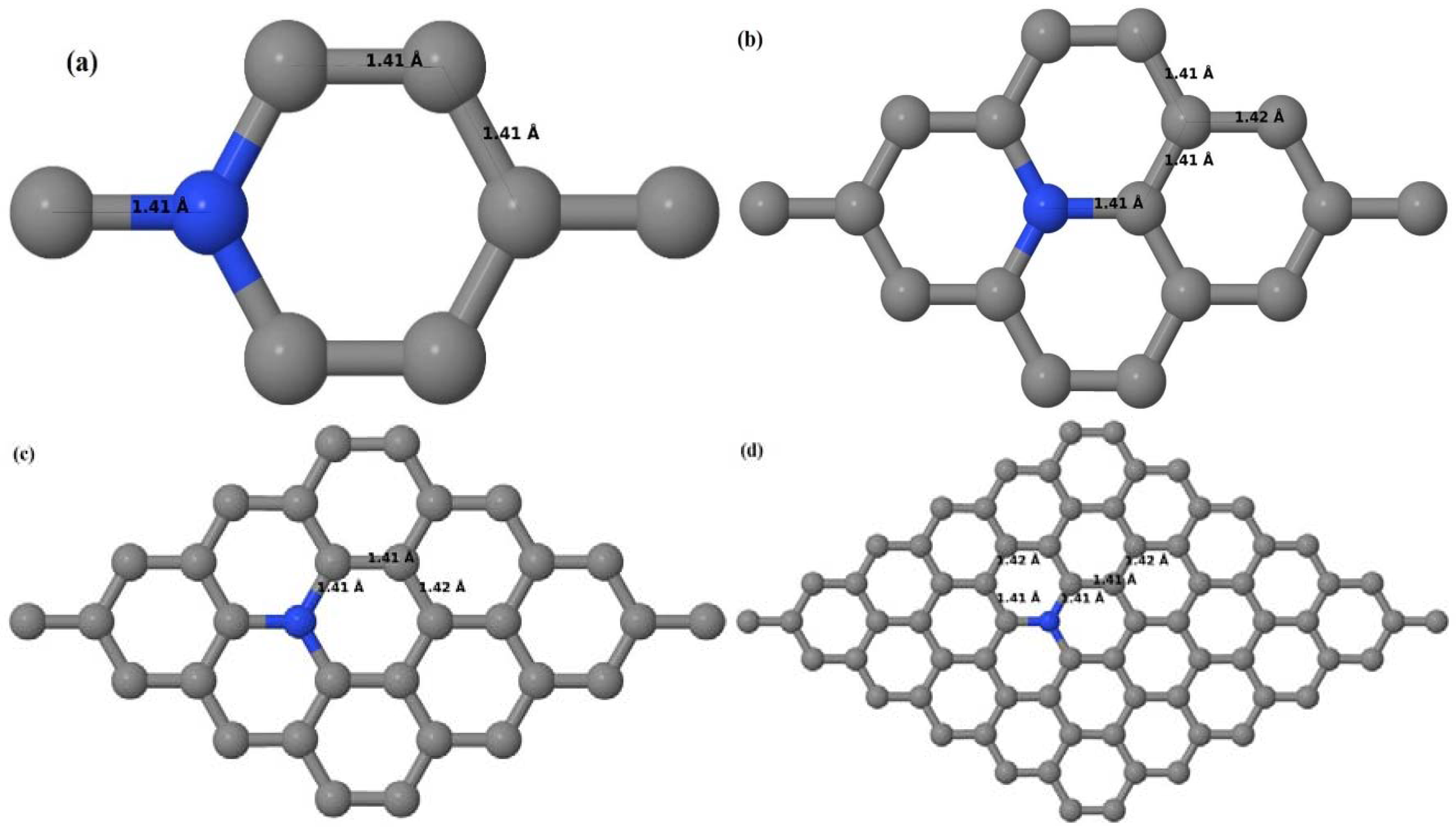
3.2.1. B-Doped Graphene System with One B Atom per Supercell
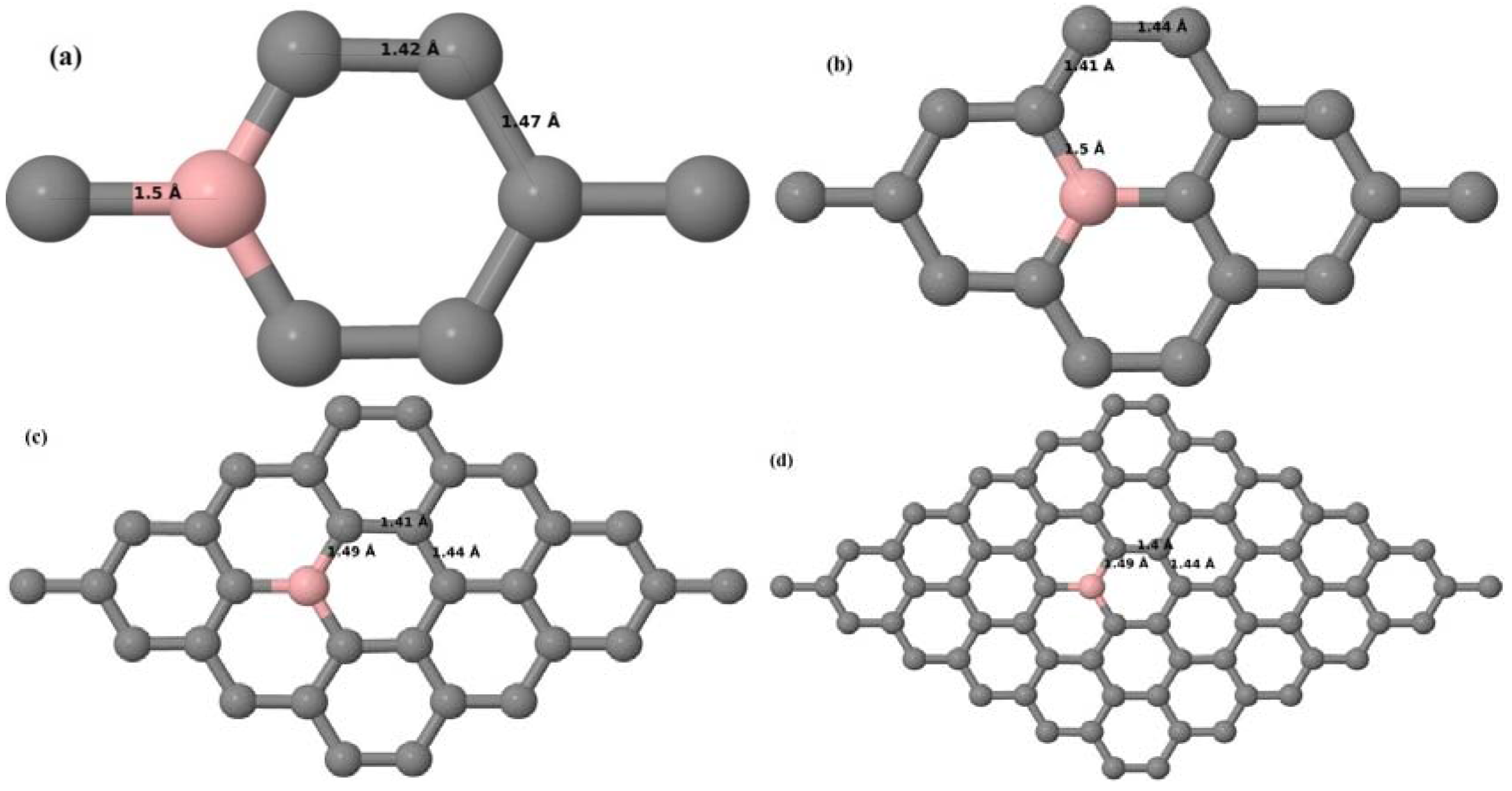
Here, we consider one B substitutional dopant in 2 × 2, 3 × 3, 4 × 4, and 6 × 6 graphene supercells. Upon structural optimization of all graphene supercells doped with one B atom, it was observed that the planar geometry of PG remains undisturbed (
Figure 3a–d) even after the introduction of B atom, as B also undergoes
sp2 hybridization like the other C atoms in the crystal lattice, which is in accordance with earlier results [
30,
37]. The optimized lattice constant increases from 2.458 Å to 2.464 Å, 2.471 Å, 2.482 Å, and 2.514 Å for 6 × 6, 4 × 4, 3 × 3, and 2 × 2 supercells doped with one B atom (1.39%, 3.13%, 5.56%, 12.5% B concentrations), respectively. Since the atomic radius of B is larger than that of C, the lattice constant increases with the increase in the B-doping concentration, showing agreement with previous reports [
30].
Figure 3a–d depict the optimized geometries of 2 × 2, 3 × 3, 4 × 4, and 6 × 6 graphene supercells doped with one B atom. The large covalent radius of B compared to that of C results in the expansion of the C–B bond length [
30,
37] to 1.5 Å for one B doping in 2 × 2 and 3 × 3 supercells (
Figure 3a,b), whereas, in 4 × 4 and 6 × 6 supercells, the C–B bond length was extended to 1.49 Å (
Figure 3c,d) [
30,
37] from the ideal C–C bond length of 1.42 Å. The C–C bond lengths adjacent to the B atom were reduced from 1.42 Å to 1.41 Å for 3 × 3 and 4 × 4 graphene supercells (
Figure 3b,c), whereas, in the case of the 6 × 6 graphene supercell, it was reduced to 1.4 Å (
Figure 3d) in order to compensate for the long C–B bond in the crystal structure so as to retain the planar geometry. The observed reduction in the C–C bond length in the close proximity to the B atom is in agreement with the results reported in [
30]. The calculated cohesive energies per atom of the relaxed geometries of graphene systems doped with one B atom are presented in
Table 1.
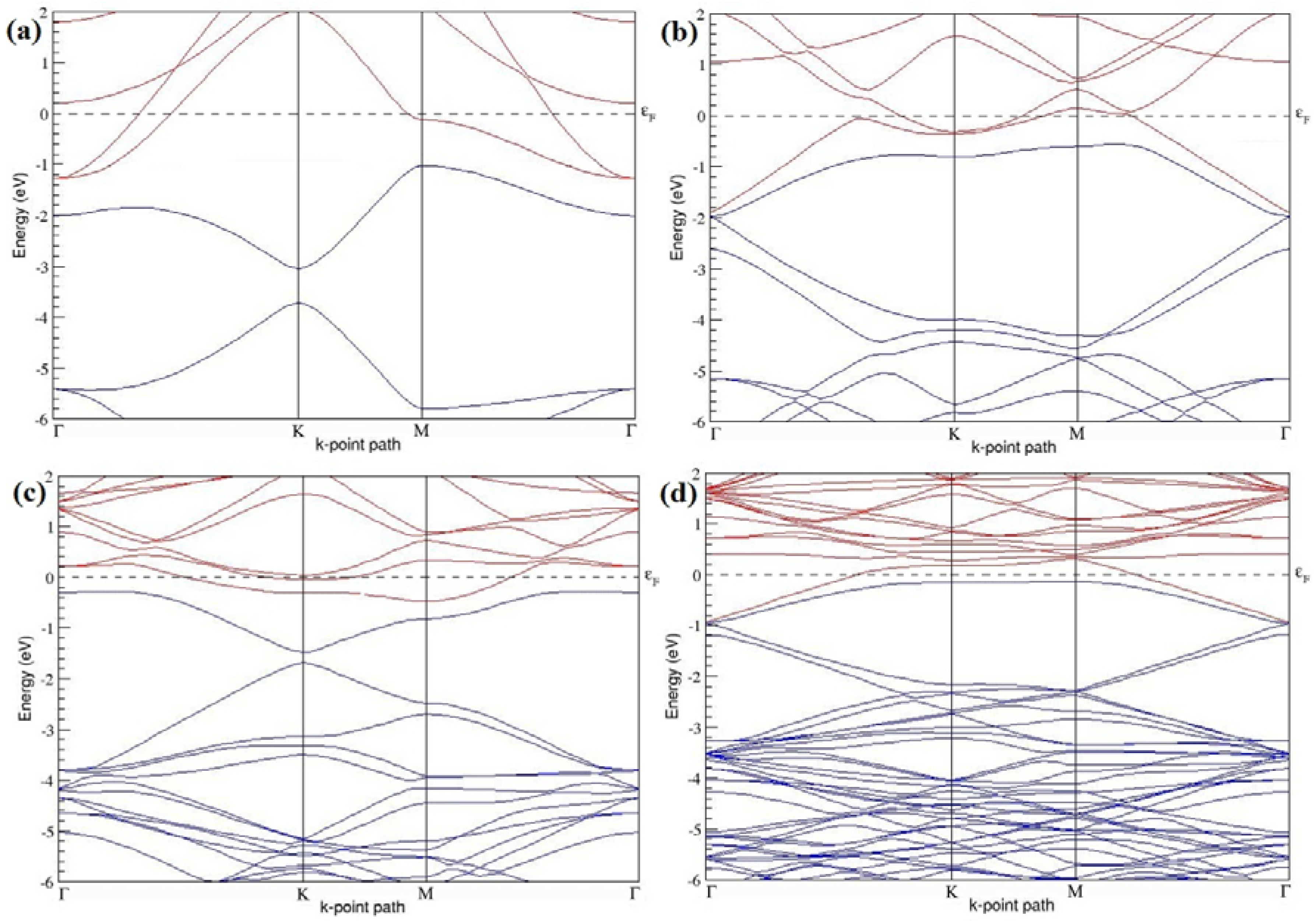
Figure 4a–d present the band structures computed for the optimized structures of different graphene systems doped with one B atom shown in
Figure 3a–d. Since the planar geometry of graphene is well preserved even after one B doping, the linear energy dispersion remains unaltered along the high symmetry points of the Brillouin zone as seen in
Figure 4a–d, similar to the reported literature [
30,
37]. Due to the symmetry breaking of the graphene sublattices by the introduction of the B atom, the band structures of 2 × 2 and 4 × 4 graphene supercells show a band gap of ~0.66 eV (
Figure 4a) and ~0.19 eV (
Figure 4c) at the Dirac point for one B-atom doping (corresponding to 12.5% and 3.13% B concentrations), respectively. The present results are slightly greater that the values reported in [
42], probably due to the variation in the employed computational method. The 3 × 3 and 6 × 6 graphene supercells doped with one B atom (corresponding to 5.56% and 1.39% B concentrations) do not show any band gap (
Figure 4b,d), which is found to be in agreement with the reported zero band gap phenomenon in 3N × 3N graphene supercells [
38,
42,
44]. In general, the energy gap increases from ~0.19 eV to ~0.66 eV for 4 × 4 and 2 × 2 supercells doped with one B atom (3.13% and 12.5% B concentrations), respectively (
Table 1).
Both 2 × 2 and 4 × 4 graphene supercells doped with one B atom exhibit p-type doping electronic properties with band gaps, whereas the 3 × 3 and 6 × 6 graphene supercells doped with one B atom show p-type doping properties with zero band gap.
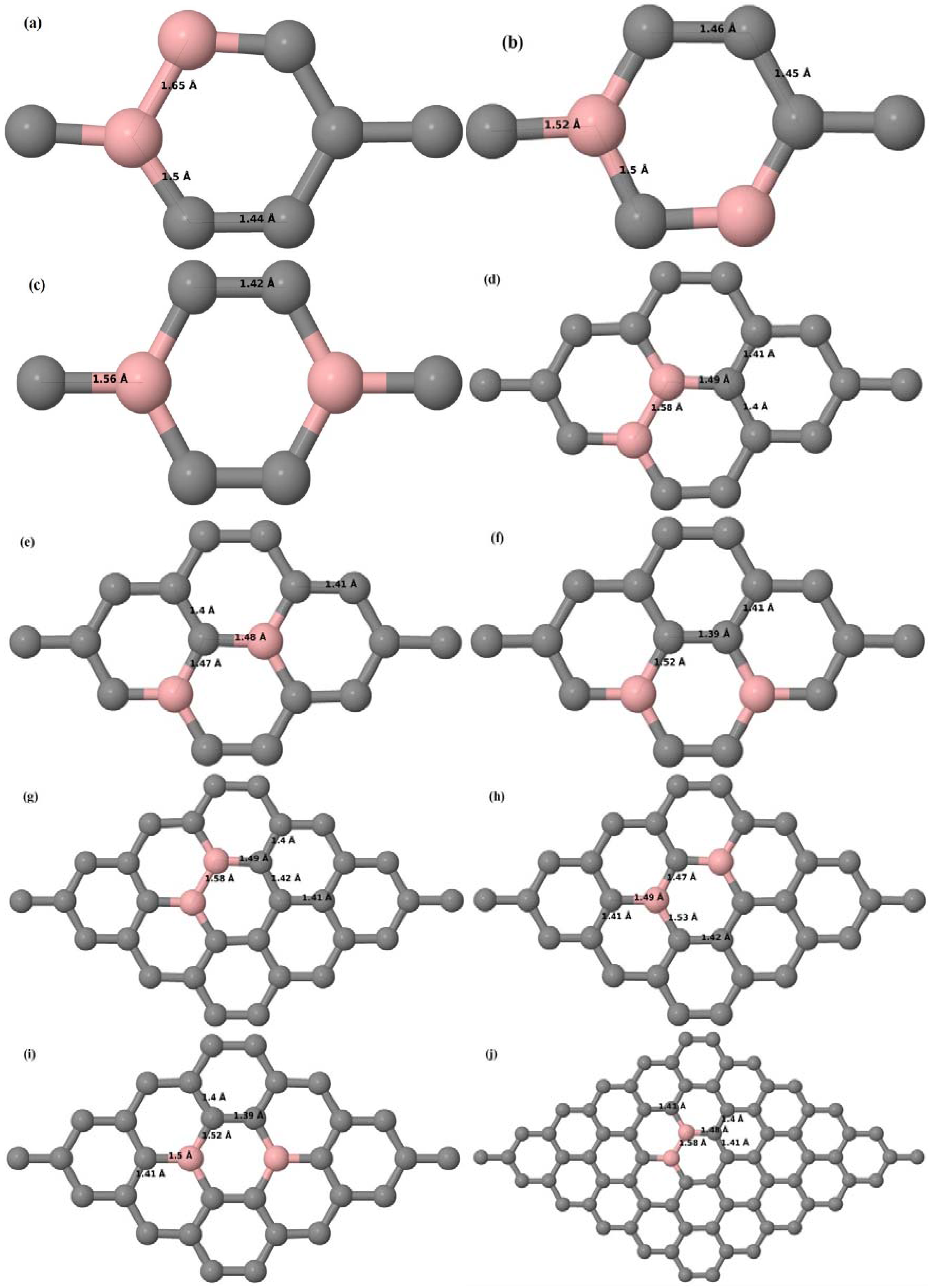
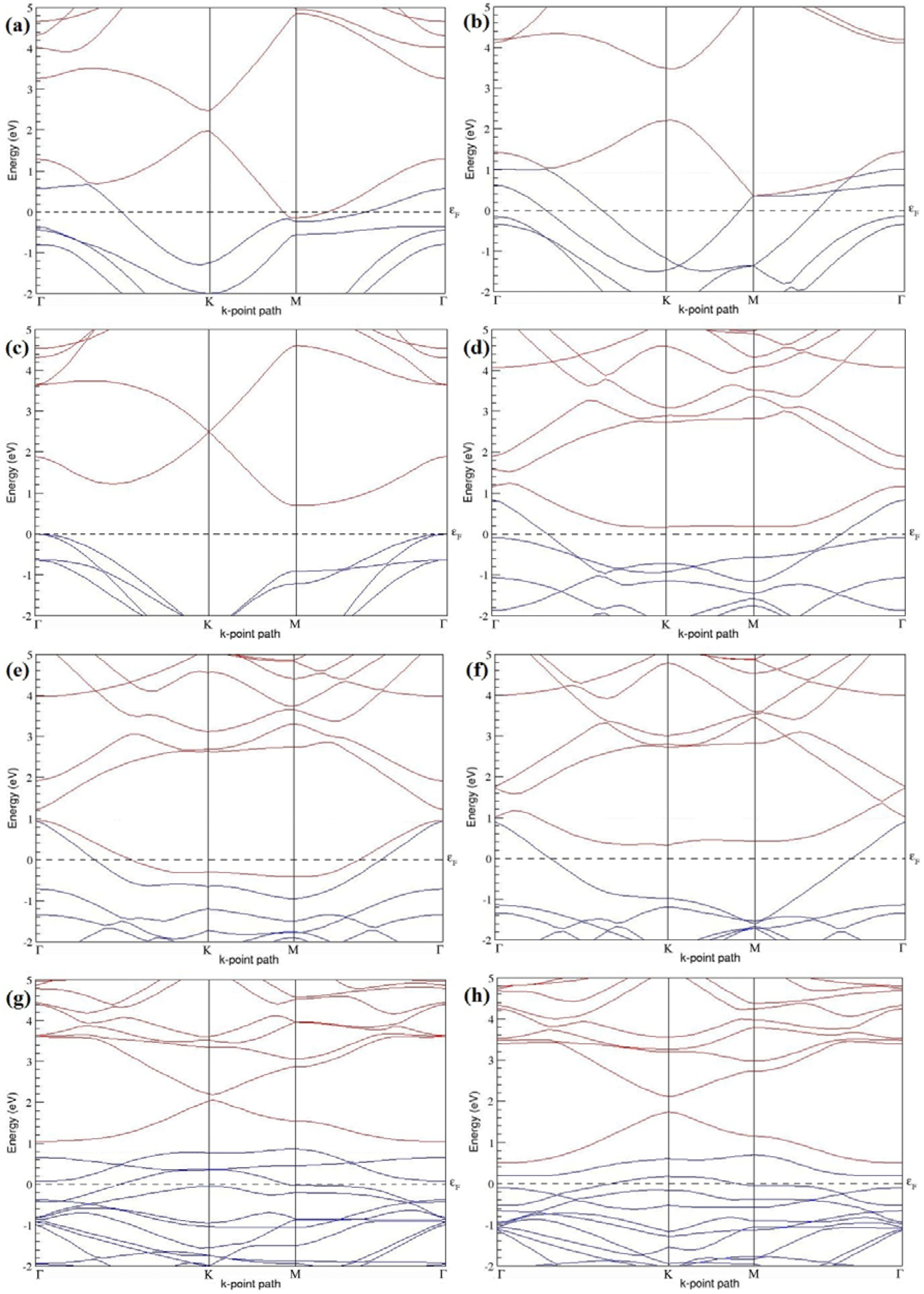
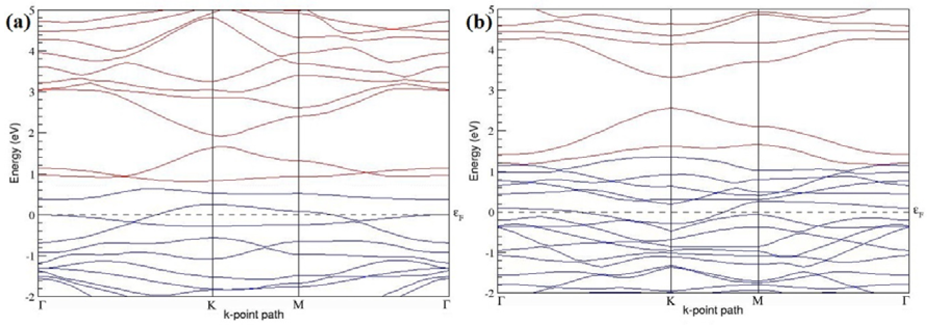
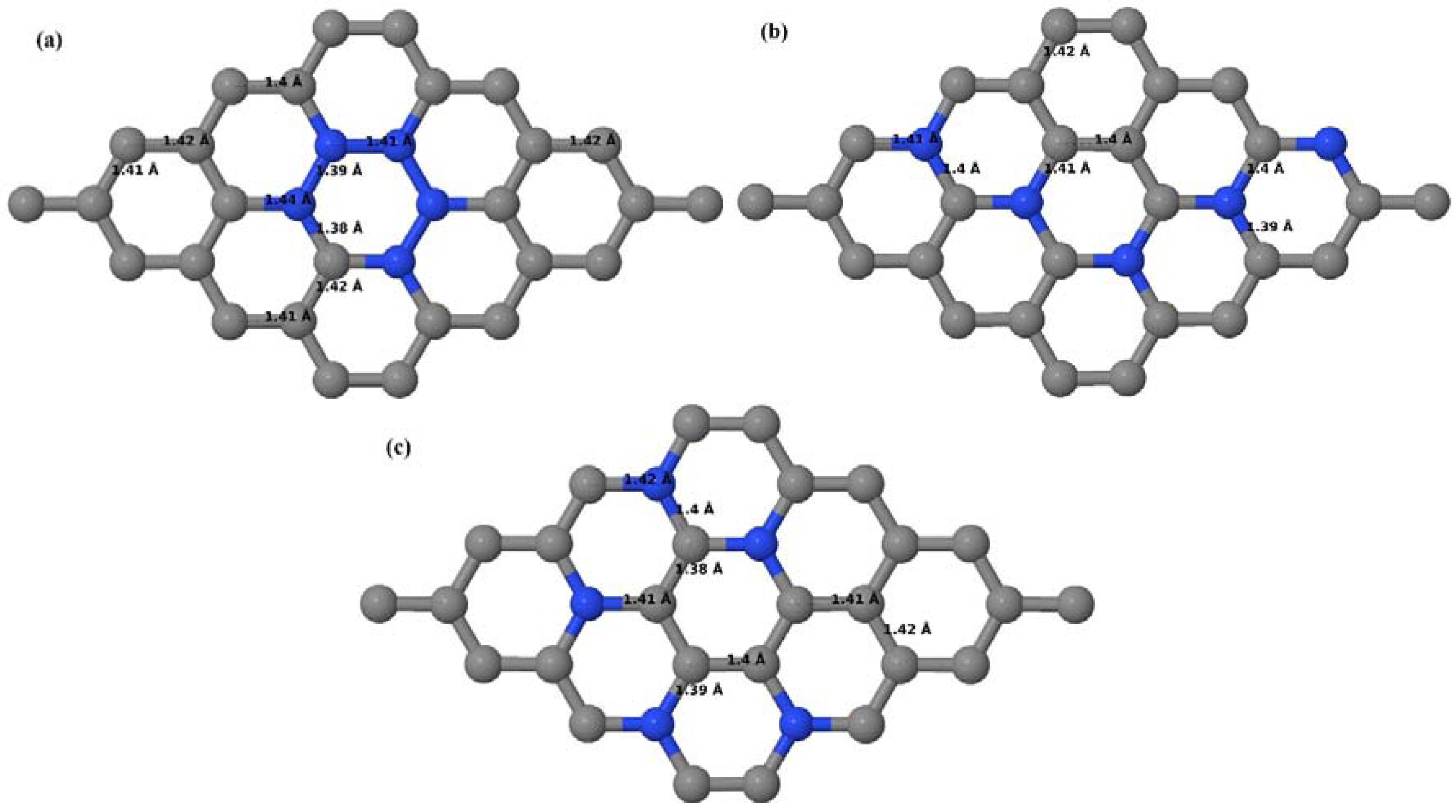
3.2.2. B-Doped Graphene System with Two B Atoms per Supercell
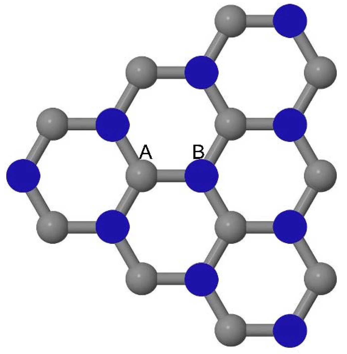
As graphene’s honeycomb lattice consists of two interpenetrating triangular sublattices as shown in
Figure 5, several isomers of the same doping concentration are possible. A few isomers with configurations of three doping sites, i.e., when all the dopant atoms are adjacent, when they are at same sublattice positions (all in either sublattice “A” or in sublattice “B”), and when they are at different sublattice positions (in sublattice “A” and “B”), are only presented here for simplicity, as all possible doping configurations of any atomic doping concentration will fall under these three categories only. Hence, the cohesive energies and the band structures of the above-mentioned geometries corresponding to the same doping concentration are calculated to analyze the influence of the dopant sites on the stabilities and the band gap values.
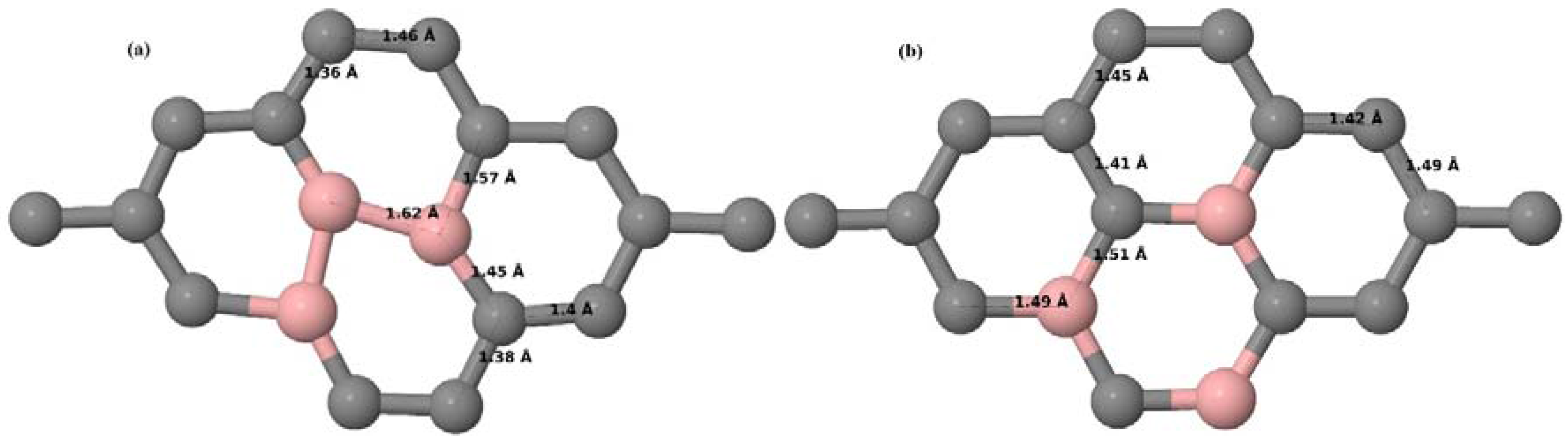
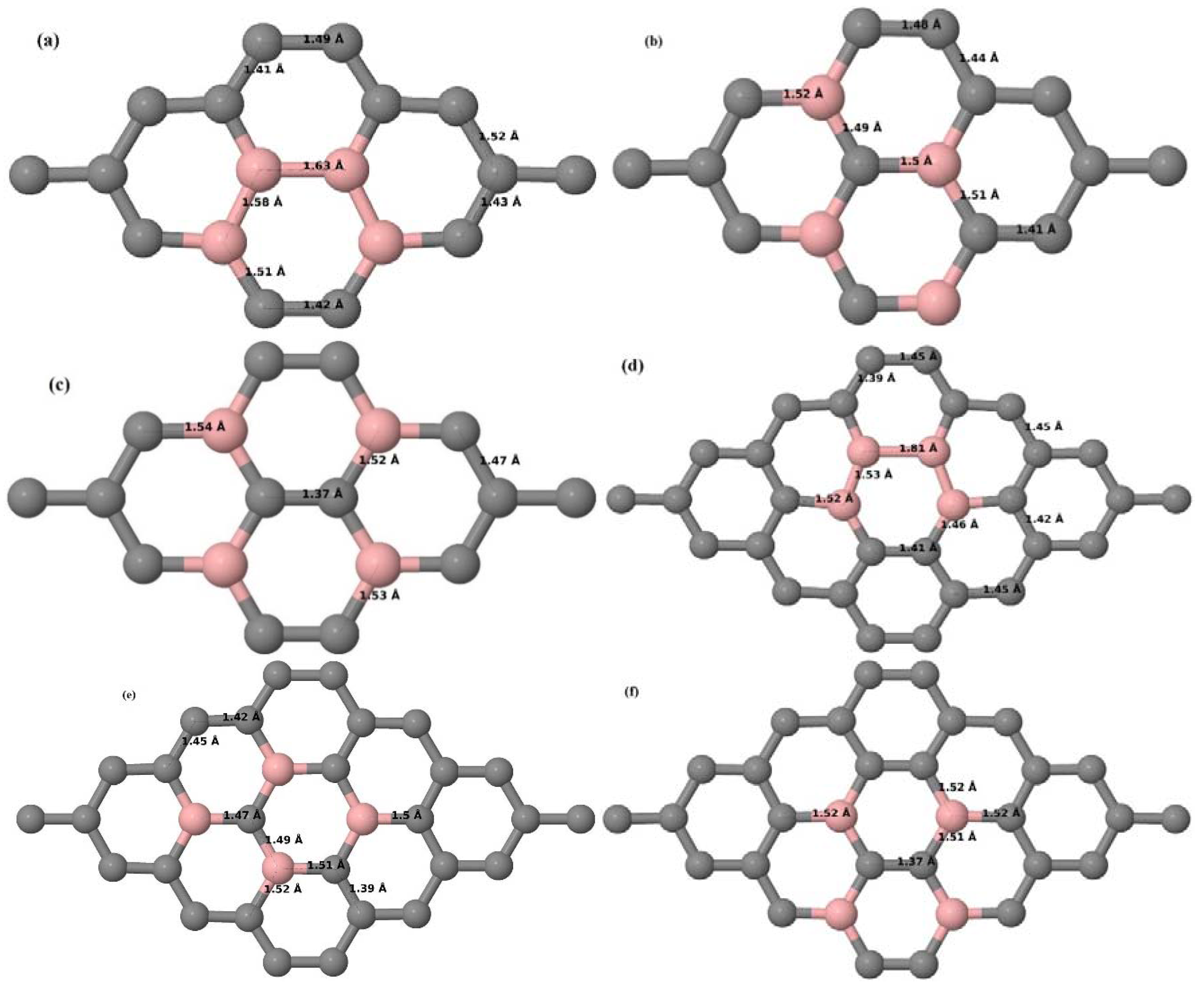
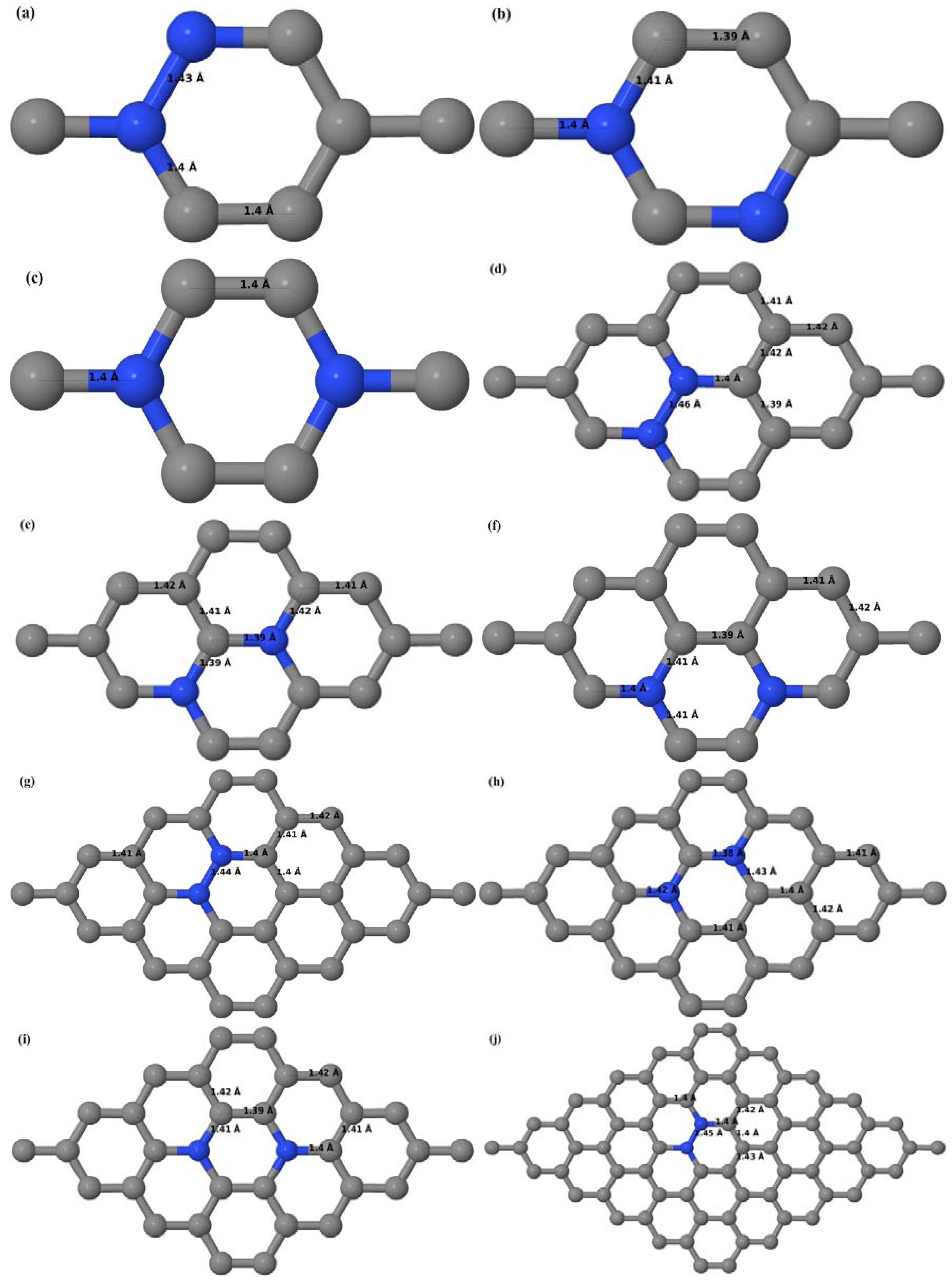
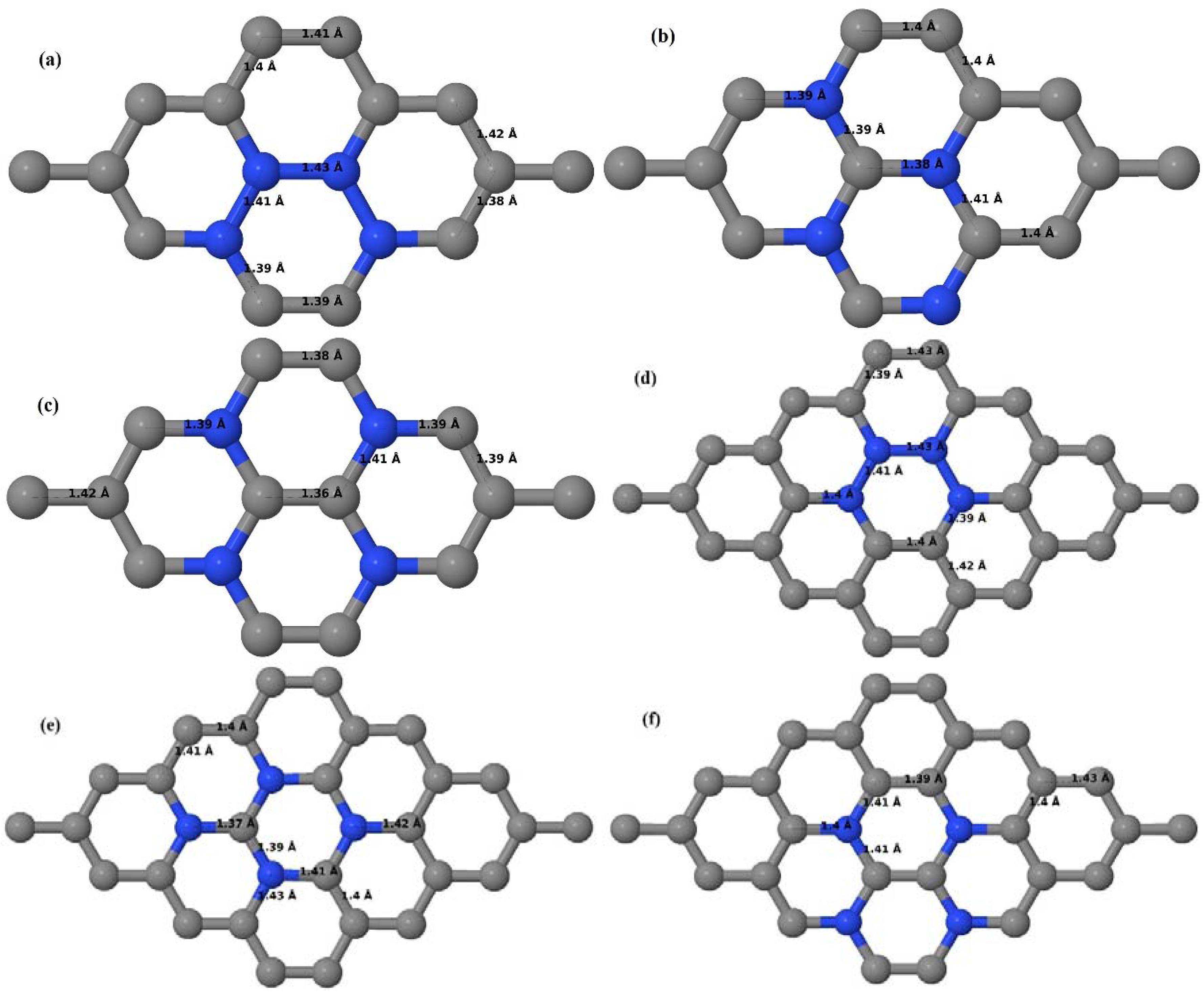
Here we consider the substitution of two C atoms by two B atoms in 2 × 2, 3 × 3, 4 × 4, and 6 × 6 graphene supercells (
Figure 6a–l). Similar to graphene systems doped with one B atom, the graphene systems doped with two B atoms also retain the planar geometry of PG as seen in
Figure 6a–l. The optimized lattice constant increases from 2.458 Å to 2.469 Å, 2.484 Å, 2.504 Å, and 2.576 Å for 6 × 6, 4 × 4, 3 × 3, and 2 × 2 supercells doped with two B atoms (2.78%, 6.25%, 11.11%, and 25% B concentrations), respectively, which also shows an increase in lattice constant with increasing B-doping concentration similar to that observed for graphene systems doped with one B atom.
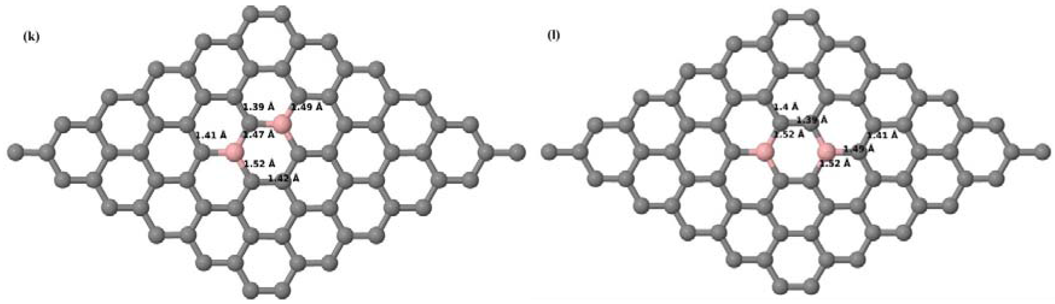
Figure 6a–l depict the optimized geometries of the 2 × 2, 3 × 3, 4 × 4, and 6 × 6 graphene supercells doped with two B atoms. Three doping configurations of the 2 × 2, 3 × 3, 4 × 4, and 6 × 6 supercells doped with two B atoms (corresponding to 25%, 11.11%, 6.25%, and 2.78% B concentrations, respectively) are considered with the dopant atoms at adjacent, (
Figure 6a,d,g,j), same (
Figure 6b,e,h,k), and alternate sublattice points (
Figure 6c,f,i,l). The C–B bond length was expanded significantly (
Figure 6a–l) as compared to graphene systems doped with one B atom, due to the presence of the two B atoms, which have a bigger size compared to the other C atoms in the lattice, whereas the C–C bond length in close proximity of the dopant was shortened from 1.42 Å to 1.41 Å or 1.4 Å, or even to 1.39 Å, in most of the optimized structures, based on the position of the B dopants, in an attempt to the preserve the planar lattice structure. After obtaining stable geometries, the cohesive energies were calculated for all the considered graphene systems doped with two B atoms and are listed in
Table 2.
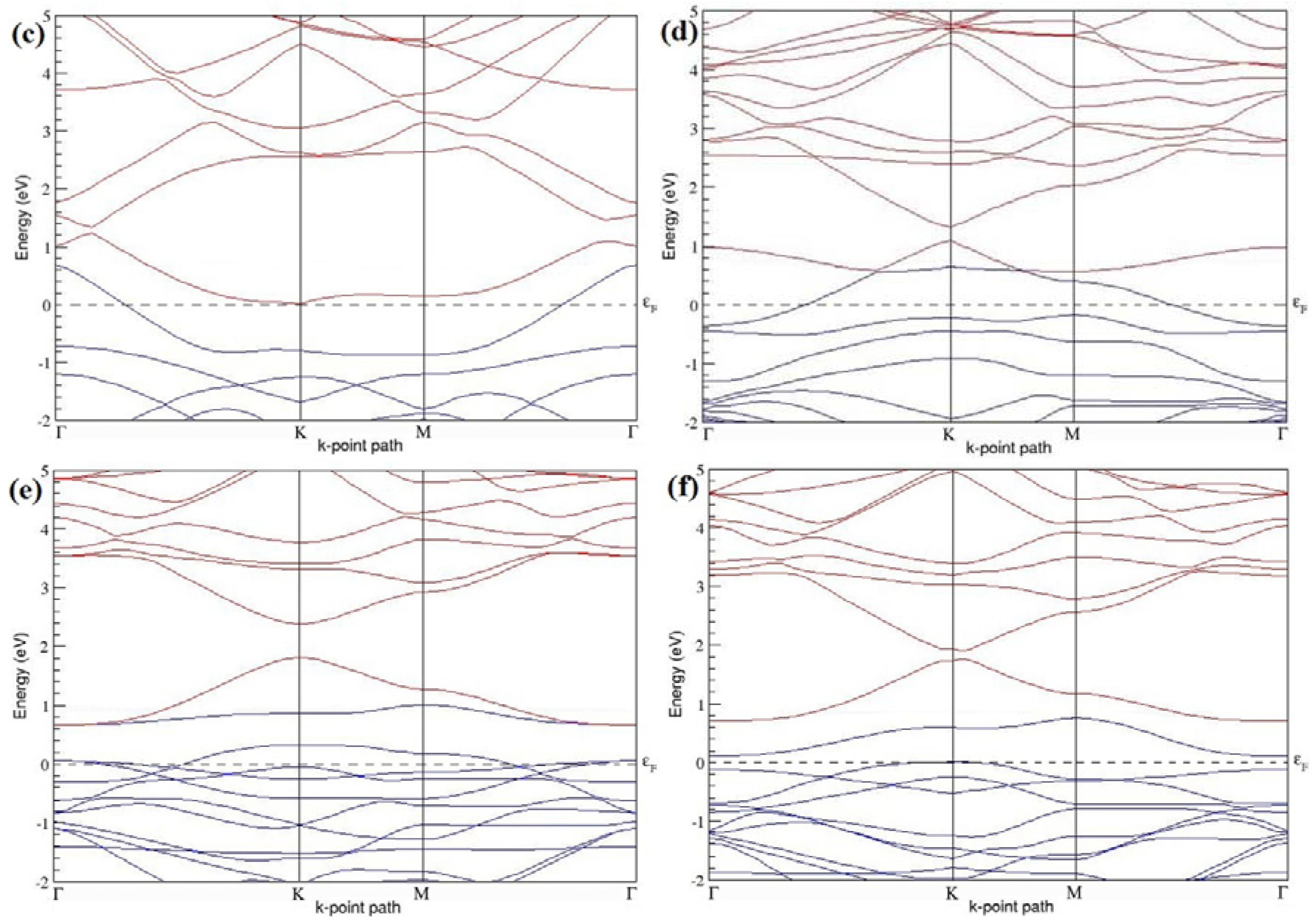
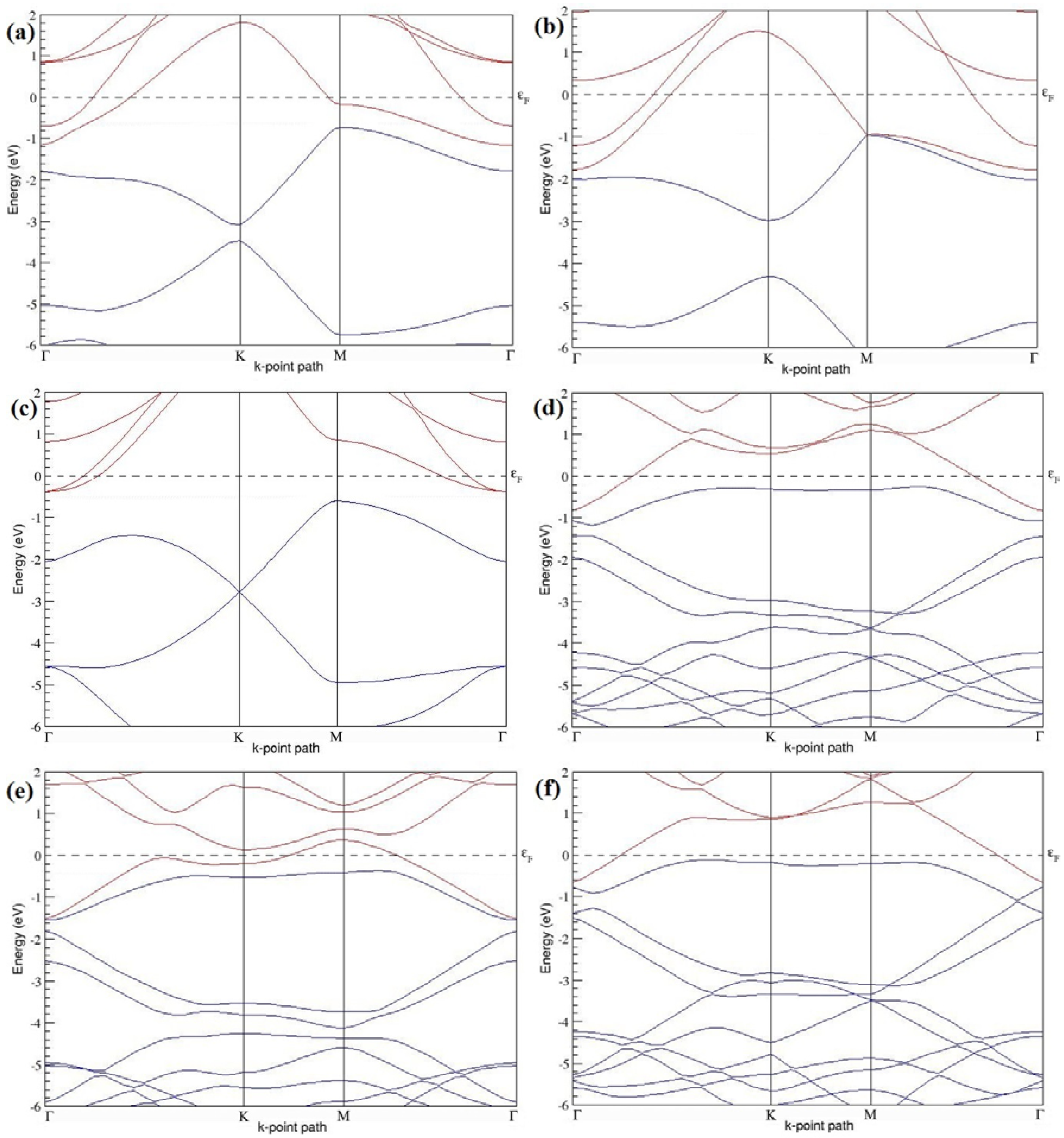
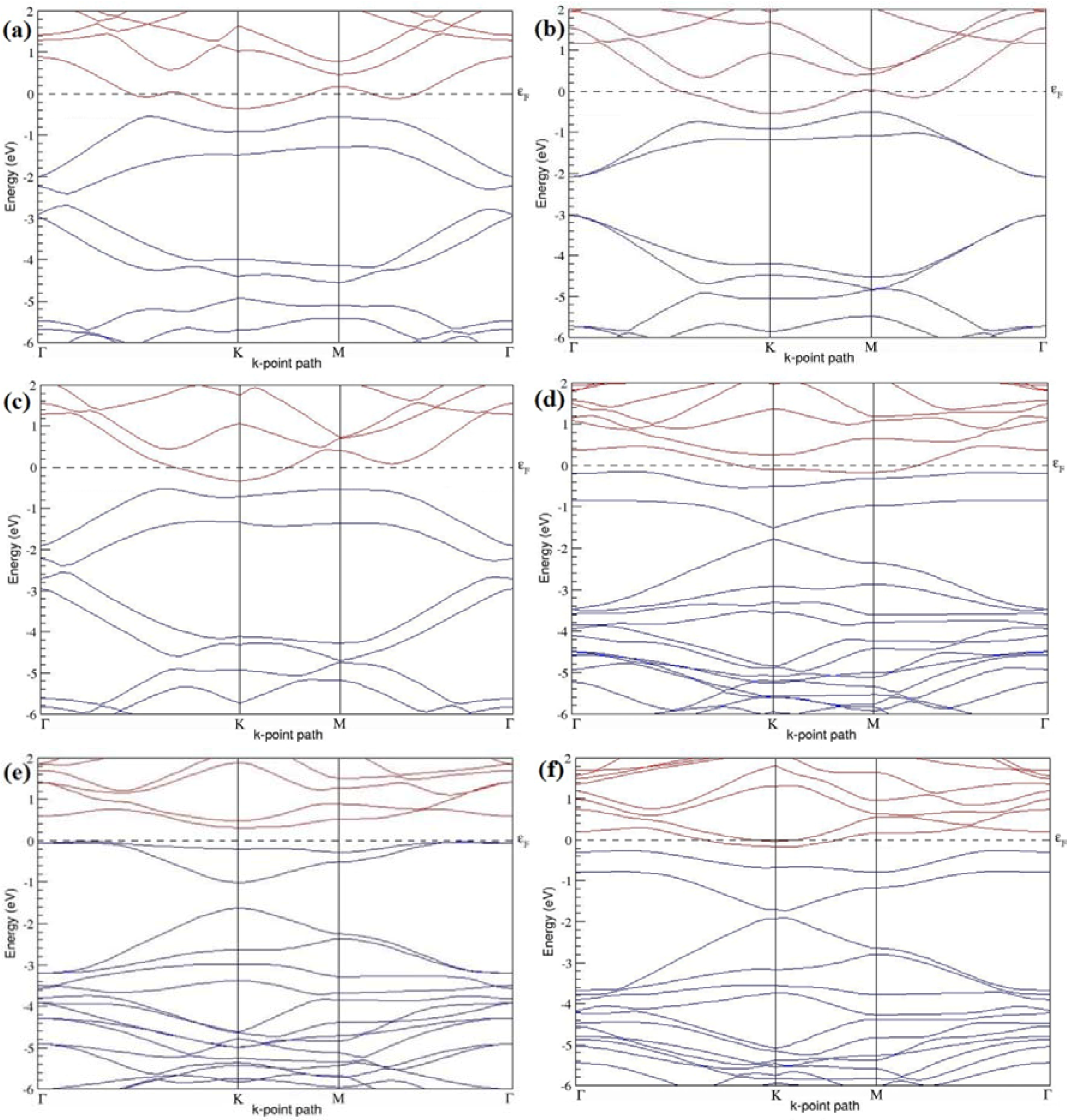
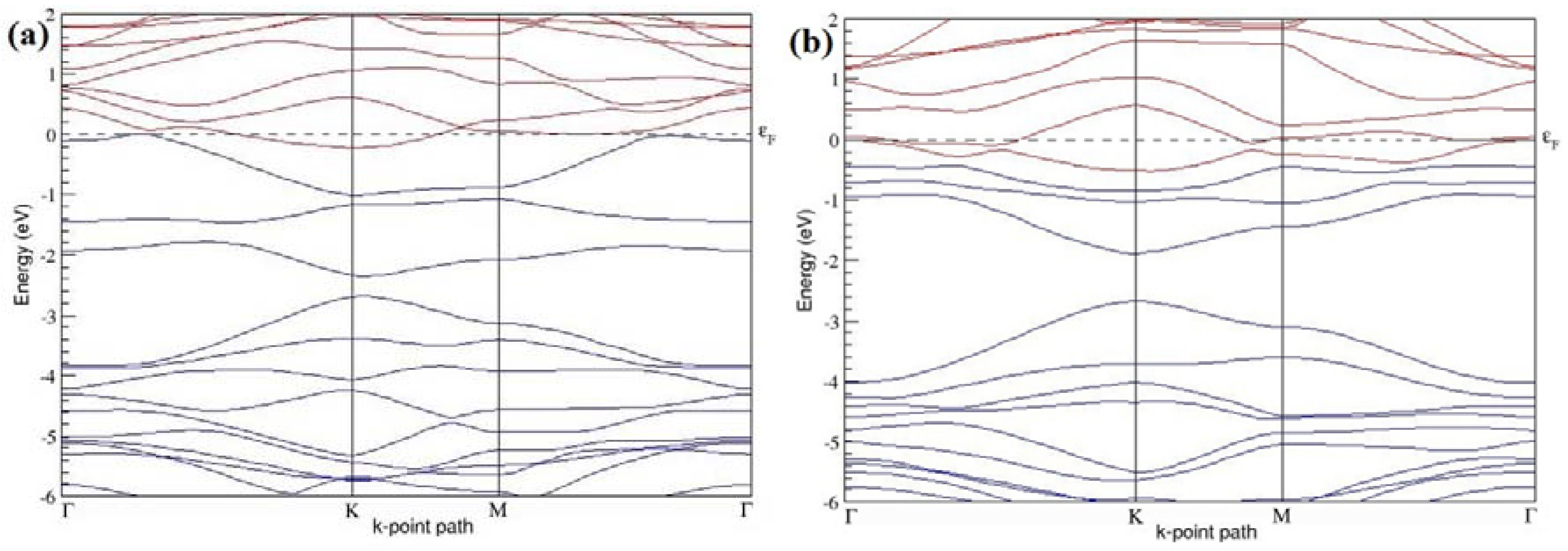
Figure 7a–l present the band structures computed for the optimized structures of different B-doped graphene systems shown in
Figure 6a–l. As seen in
Figure 7a–l, the linear dispersion around the Dirac point is not completely destroyed, but an energy band gap opens in all cases except for graphene doped with two B atoms into the 2 × 2 graphene supercell with dopant atoms at the alternate sublattice points (
Figure 7c). The 2 × 2 graphene supercell doped with two B atoms (corresponding to 25% B concentration) shows band gaps of ~0.49 eV (
Figure 7a) and ~1.28 eV (
Figure 7b) upon placing the B atoms at adjacent and same sublattice positions, respectively, in graphene. B-doped graphene with 25% B concentration has a zero gap (
Figure 7c) when the B atoms are at alternate sublattice positions due to the symmetry formed by the B atoms situated in two graphene sublattices (“A” and “B”). At a 6.25% B concentration, band gaps of 0.13 eV (
Figure 7g), 0.375 eV (
Figure 7h), and ~0.05 eV (
Figure 7i) open up in graphene when the B atoms are placed at the adjacent, same, and alternate sublattice positions in graphene, respectively.
The band structures of 3 × 3 and 6 × 6 graphene supercells doped with two B atoms are characterized by a non-zero band gap (
Figure 7d–f,j–l), which is different from the zero band gap behavior observed for the 3 × 3 and 6 × 6 graphene supercells doped with one B atom. The 3 × 3 graphene supercells doped with two B atoms (corresponding to 11.11% B concentration) exhibit band gaps of 0.265 eV (
Figure 7d), 0.274 eV (
Figure 7e), and ~0.05 eV (
Figure 7f) for the configurations with dopants at adjacent, same, and alternate sublattices in graphene, respectively. Doping of graphene with 2.78% concentration of B results in a band gap opening of 0.10 eV (
Figure 7j), ~0.11 eV (
Figure 7k), and 0.008 eV (
Figure 7l), respectively, in graphene upon placing the B atoms at adjacent, same, and alternate sublattice sites in graphene.
The 2 × 2, 3 × 3, 4 × 4, and 6 × 6 graphene supercells doped with two B atoms exhibited
p-type semiconducting behaviors. The 2 × 2 graphene supercell doped with two B atoms also exhibit
p-type electronic behavior, but does not show any band gap when the dopants are at alternate sublattice sites (
Figure 7c). The considered B concentrations, the doping configurations along with the selected sublattices, the calculated cohesive energies, and the band gaps observed for all considered graphene systems doped with two B atoms are summarized in
Table 2.
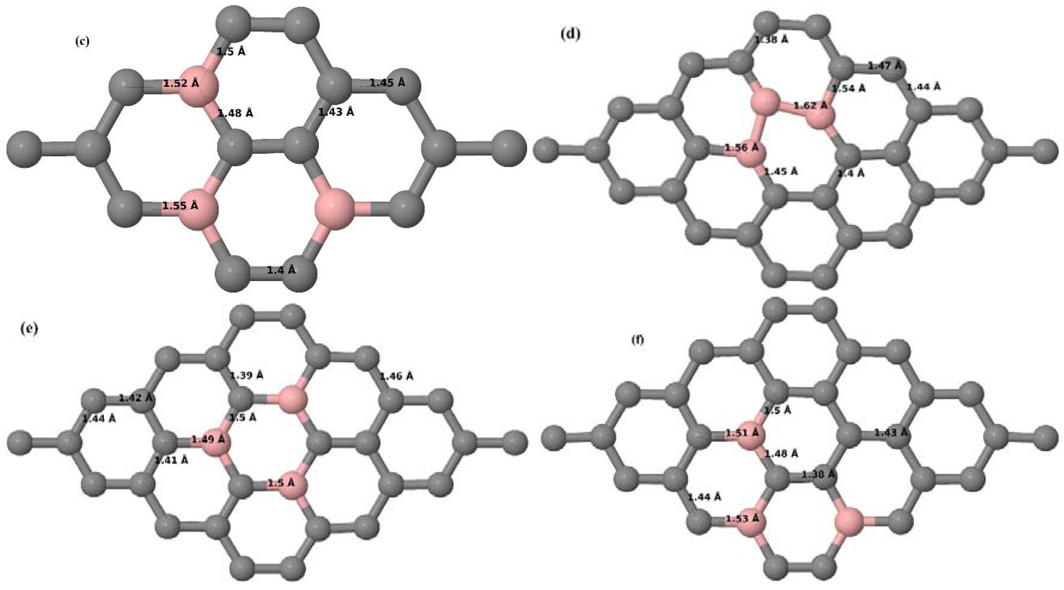
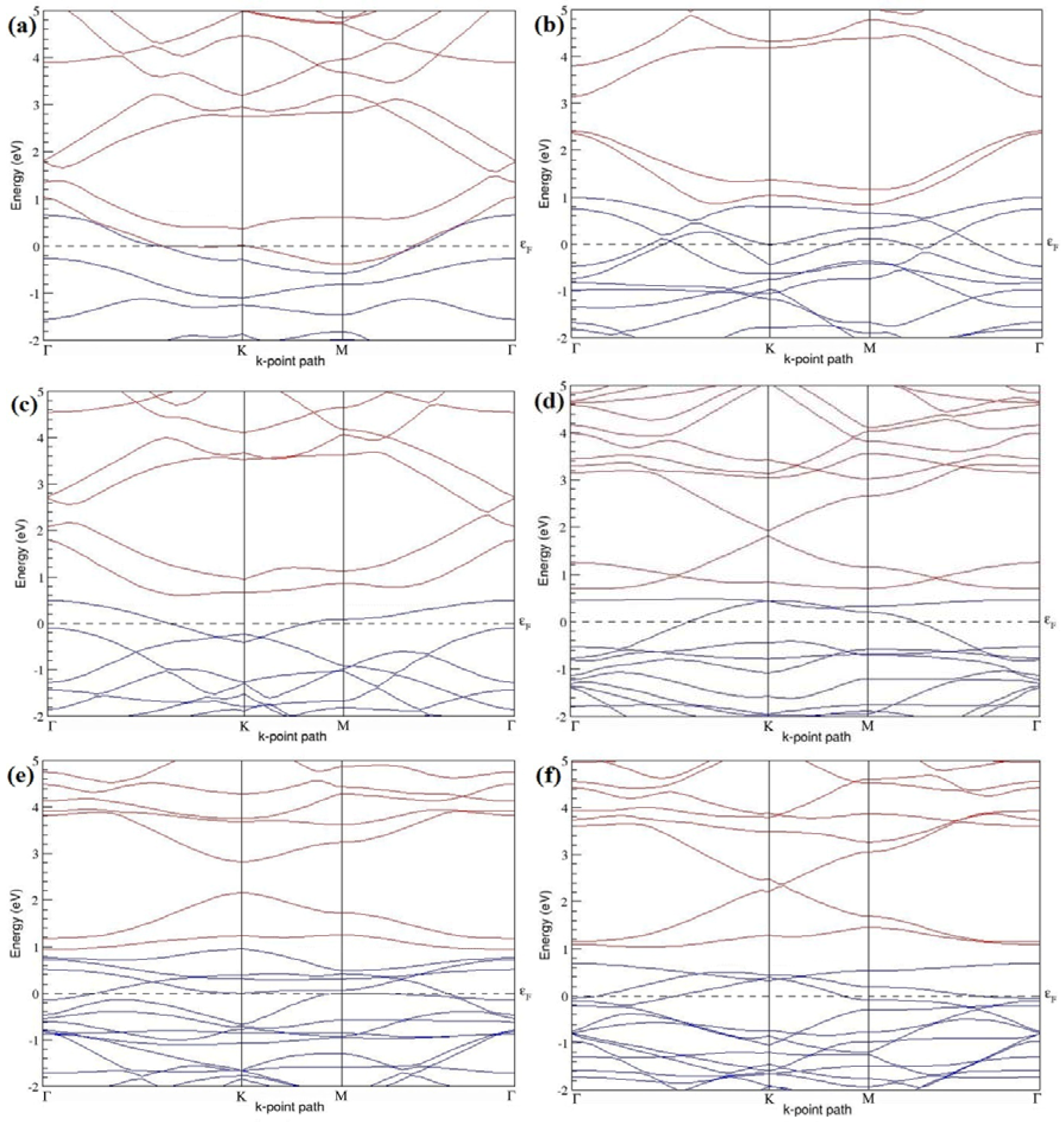
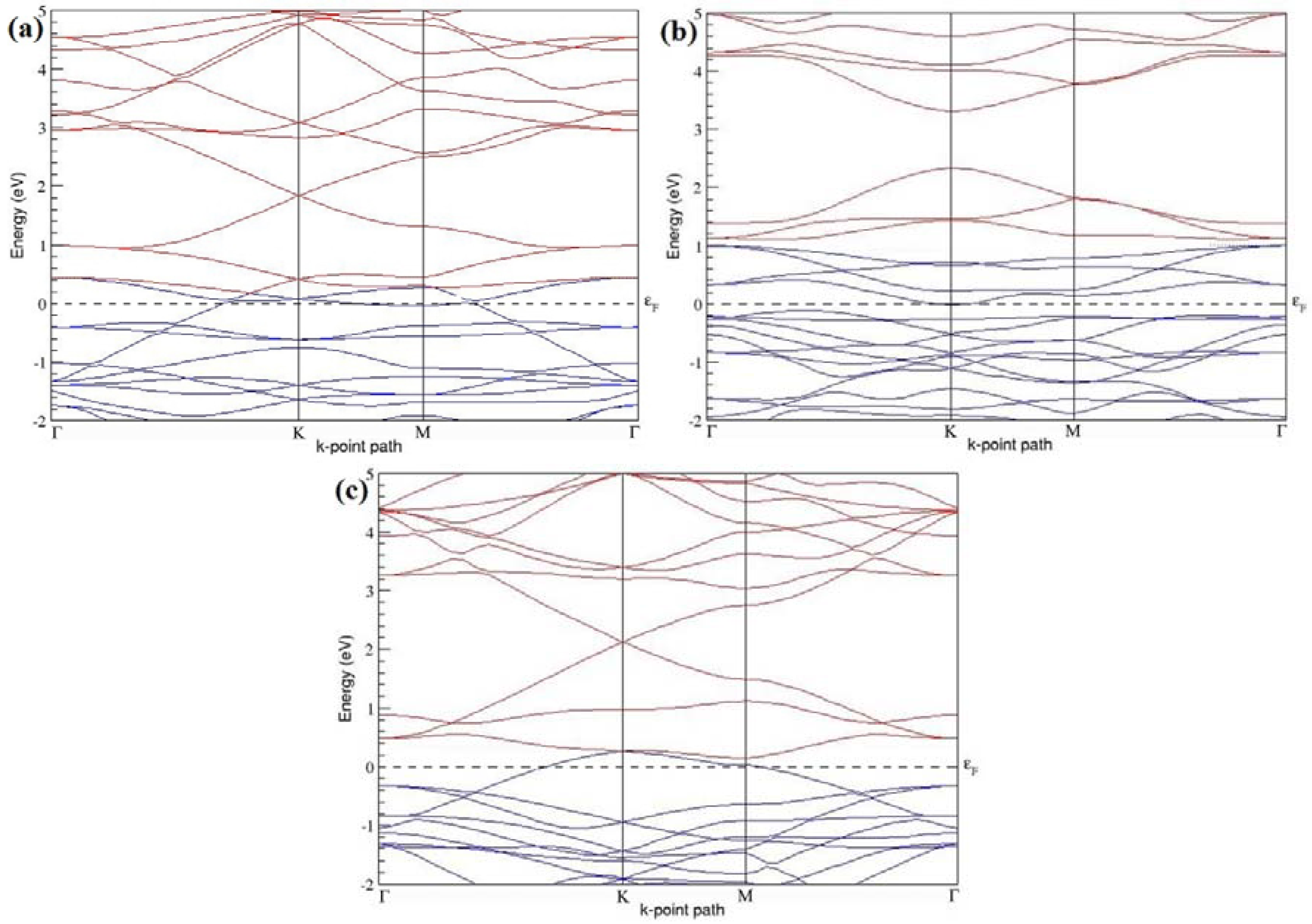
3.2.3. B-Doped Graphene System with Three B Atoms per Supercell
Here we consider the substitution of three C atoms by three B atoms in 3 × 3 and 4 × 4 graphene supercells. Similar to graphene systems doped with one and two B atoms, the planar lattice structure of graphene remains the same (
Figure 8a–f) even after the introduction of three B atoms. The optimized lattice constant increases from 2.458 Å to 2.475 Å and 2.528 Å for 4 × 4 and 3 × 3 supercells doped with three B atoms (9.38% and 16.67% B concentrations), respectively, which indicates increase in lattice constant with doping concentration similar to that seen in graphene systems doped with one and two B atoms.
Figure 8a–f present the relaxed geometries of 3 × 3 and 4 × 4 graphene supercells doped with three B atoms at adjacent, same, and alternate sublattices, respectively. After structural optimization, it was found that graphene structures doped with three B atoms at adjacent locations experience significant geometrical distortion (
Figure 8a,d) due to the positioning of three B atoms in the same six-membered carbon ring, as compared to the other graphene systems doped with three B atoms. However, the three adjacent B atoms are still seen to lie within the plane with large adjustments in the adjoining bond lengths (
Figure 8a,d).
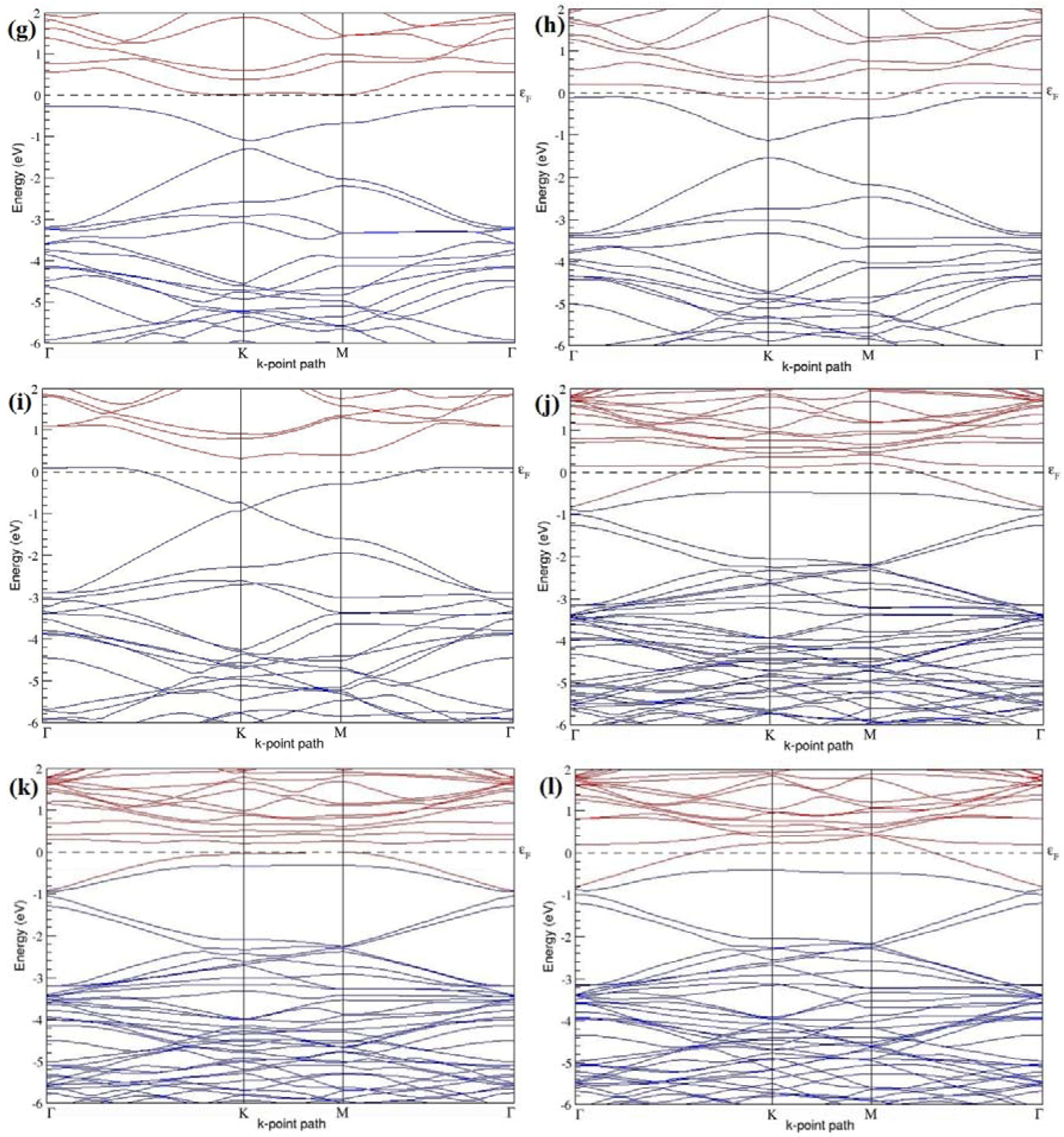
Figure 9a–f present the band structures computed for the optimized structures of different graphene systems doped with three B atoms shown in
Figure 8a–f. The band structures of both 3 × 3 and 4 × 4 graphene supercells doped with three B atoms show non-zero band gaps as seen in
Figure 9. The linear energy dispersion at the Dirac point in the band structures of graphene systems doped with three B atoms is found to be greatly affected (
Figure 9a,d) for those structures in which the B-substitutional dopants are placed at the adjacent positions (
Figure 8a,d), which could be attributed to their highly distorted geometries. The observation of highly deformed band structures of B-doped graphene with an odd number of dopants in adjacent positions is consistent with that reported in [
30].
At a 16.67% B concentration, the observed band gaps are ~0.03 eV (
Figure 9a) and ~0.11 eV (
Figure 9c), when the dopant atoms are placed at the adjacent and alternate sublattices, respectively. The positioning of the three B atoms at the same sublattices leads to a large band gap opening of ~0.90 eV (
Figure 9b) at a 16.67% B concentration. Graphene with a 9.38% B concentration shows band gaps of 0.235 eV (
Figure 9d), ~0.57 eV (
Figure 9e), and ~0.16 eV (
Figure 9f), for the doping configurations of adjacent, same, and alternate sublattices, respectively.
Graphene with three B-doping atoms in 3 × 3 and 4 × 4 graphene supercells exhibit
p-type semiconducting behaviors.
Table 3 presents the models used, the B concentrations, the considered doping configurations with sublattices, the calculated cohesive energies, and the band gaps introduced for all graphene systems doped with three B atoms.
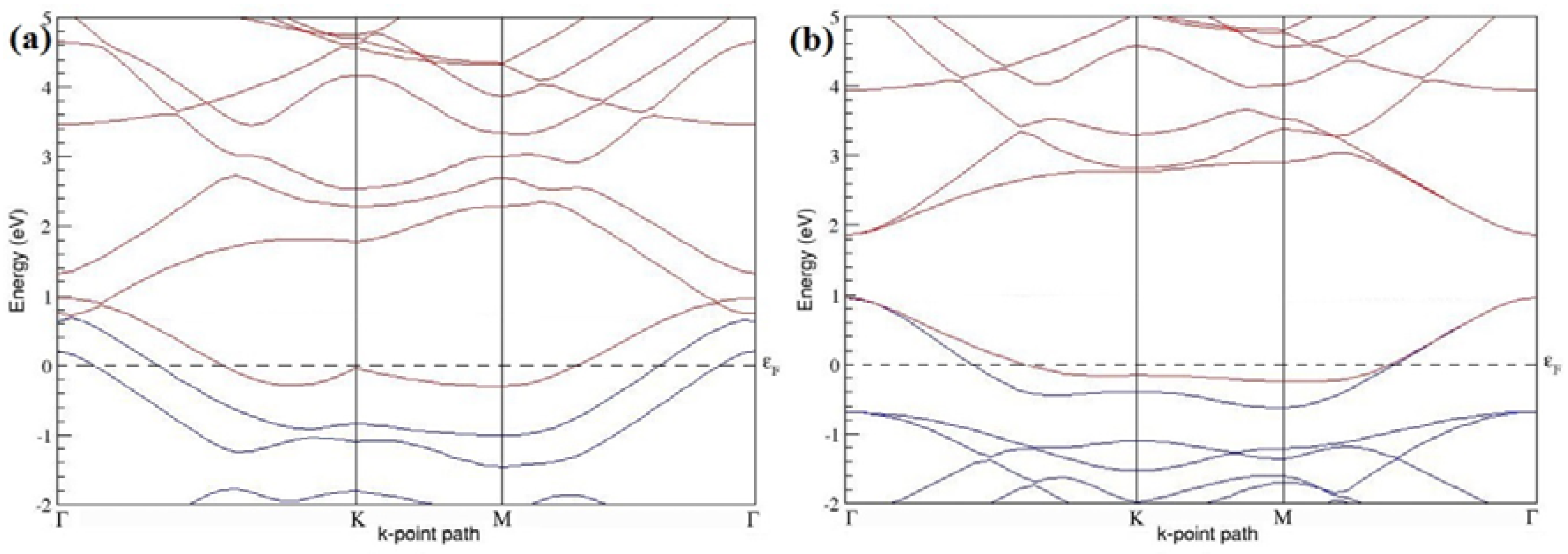
3.2.4. B-Doped Graphene System with Four B Atoms per Supercell
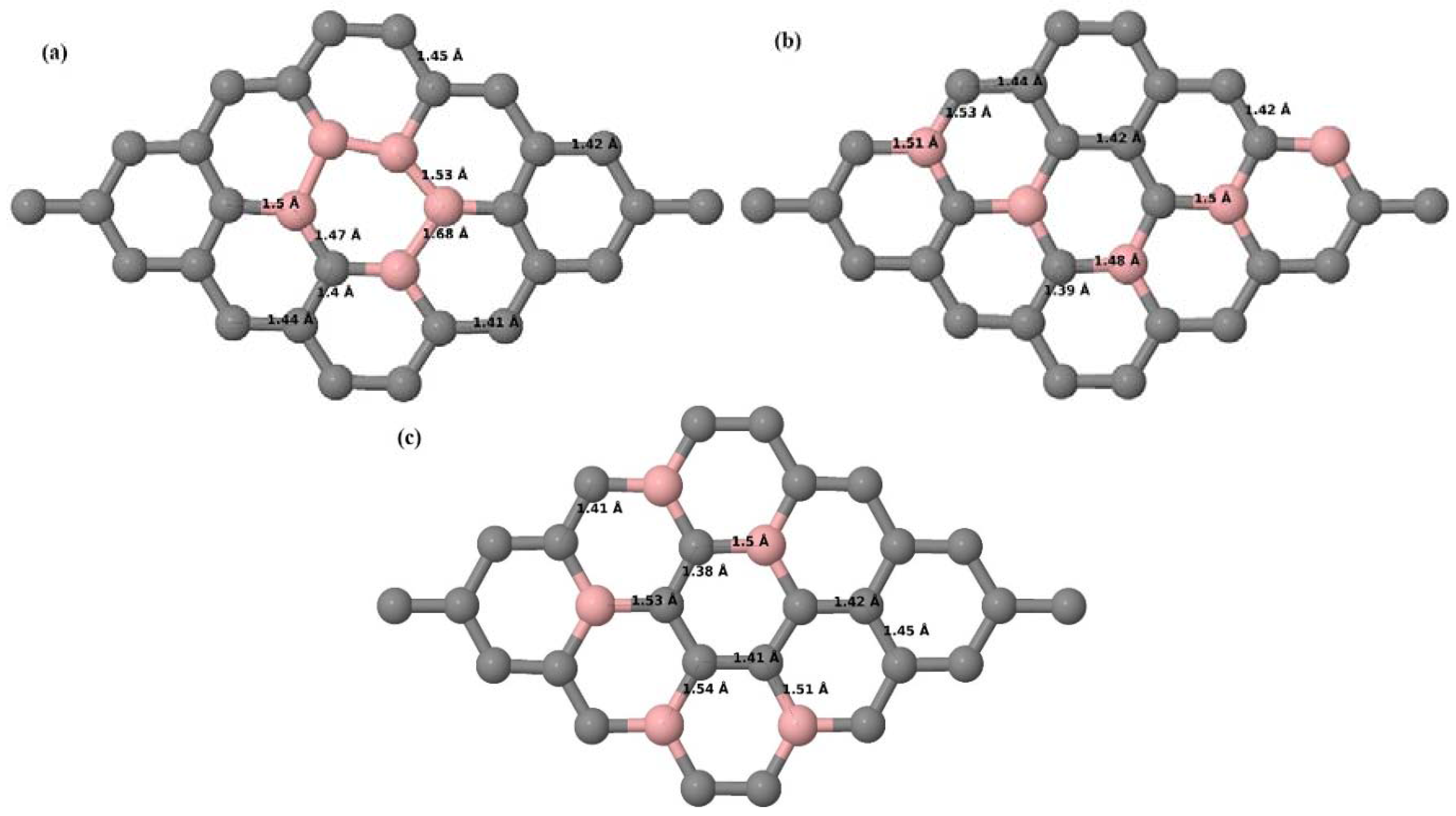
Here we consider the substitution of four C atoms by four B atoms in 3 × 3 and 4 × 4 graphene supercells. After structural relaxation, all graphene systems doped with four B atoms appear to have the same planar configuration of PG by adjusting the associated bond lengths (
Figure 10a–f). The relaxed lattice constant increases from 2.458 Å to 2.512 Å and 2.557 Å for 4 × 4 and 3 × 3 supercells doped with four B atoms (corresponding to 12.5% and 22.22% B concentrations), respectively, similar to that observed in other B-doped graphene systems.
Figure 10a–f present the relaxed structures of 3 × 3 and 4 × 4 supercells doped with four B atoms at adjacent, same, and alternate sublattices, respectively. As compared with graphene systems doped with three B atoms, graphene systems doped with four B atoms experience much less structural distortion when the B atoms are placed at adjacent positions in the lattice (
Figure 10a,d).
Figure 11a–f present the band structures computed for the optimized structures of different graphene systems doped with four B atoms shown in
Figure 10a–f. The band structures of both 3 × 3 and 4 × 4 graphene supercells doped with four B atoms depicted in
Figure 11a–f show non-zero band gap values. At a 22.22% B concentration, the doped graphene exhibits band gaps of 0.096 eV (
Figure 11a), ~0.73 eV (
Figure 11b), and ~0.06 eV (
Figure 11c) when B atoms are at adjacent, same, and alternate sublattices, respectively. Graphene with 12.5% B concentration shows band gaps of ~0.12 eV (
Figure 11d) and ~0.05 eV (
Figure 11f) for the doping configurations of adjacent and alternate sublattices, respectively. A maximum band gap of ~0.66 eV (
Figure 11e) opens up in graphene at a 12.5% B concentration, when the dopant atoms are at the same sublattice.
All graphene structures doped with four B atoms exhibit
p-type semiconducting behaviors.
Table 4 presents the models used, the doping concentrations with selected sublattices, calculated cohesive energies, and the band gaps introduced for all graphene systems doped with four B atoms.
3.2.5. B-Doped Graphene System with Five B Atoms per Supercell
Here we consider the substitution of five C atoms by five B atoms in a 4 × 4 graphene supercell. After structural relaxation, it was observed that all graphene systems doped with five B atoms exhibit planar geometry (
Figure 12a–c), similar to other B-doped graphene systems. The relaxed lattice constant increases from 2.458 Å to 2.527 Å for the 4 × 4 graphene supercell doped with five B atoms (corresponding to 15.63% B concentration), as observed in other B-doped graphene systems. Similar to graphene systems doped with three B atoms, graphene systems doped with five B atoms at adjacent positions experience significant structural distortion, but the planar configuration is maintained by adjusting the C–B and adjacent C–C bond lengths (
Figure 12a). The observed structural distortion is larger than that observed in systems doped with four B atoms.
The band structures computed for the optimized structures of different graphene systems doped with five B atoms shown in
Figure 13a–c, show
p-type semiconducting nature. The observations of disturbed linear energy dispersion at the Dirac point and highly deformed band structure (
Figure 13a), for the doping configuration with five dopants at adjacent positions, is in agreement with similar previous reports [
30].
Table 5 summarizes the observed band gaps and the calculated cohesive energies for different doping configurations corresponding to 15.63% B concentration in graphene. At a 15.63% B concentration, B atoms located at adjacent, same, and alternate sublattices open band gaps of 0.245 eV (
Figure 13a), ~0.76 eV (
Figure 13b), and ~0.13 eV (
Figure 13c), respectively, in graphene.
3.2.6. B-Doped Graphene System with Six B Atoms per Supercell
Here we consider the substitution of six C atoms in a 4 × 4 graphene supercell by six B atoms in which the dopant positions at adjacent, same, and alternate sublattices are considered. The planar structure is preserved even after the introduction of six B atoms in the lattice (
Figure 14a–c). The relaxed lattice constant increases from 2.458 Å to 2.543 Å for the 4 × 4 graphene supercell doped with six B atoms (corresponding to 18.75% B concentration), as observed in other B-doped graphene systems. Similar to graphene systems doped with four B atoms, the considered 4 × 4 graphene supercell doped with six B atoms at adjacent positions experience less structural distortion (
Figure 14a) compared to systems doped with three and five B atoms.
The band structures of all graphene systems doped with six B atoms shown in
Figure 15a–c indicate
p-type semiconducting behaviors. At a 18.75% concentration, B-doped graphene does not show a band gap (
Figure 15a,c) when the B atoms are located at adjacent and alternate sublattice sites, whereas a band gap of ~0.99 eV opens up in graphene (
Figure 15b) when the six B dopants are located at the same sublattice sites of graphene, as summarized in
Table 6. The observed closed band gap in graphene doped with six B atoms (
Figure 15a,c) upon placing the dopants at adjacent and alternate sublattices could be attributed to the symmetry formed by the B dopants in two triangular sublattices [
30].
3.3. N-Doped Graphene
3.3.1. N-Doped Graphene System with One N Atom per Supercell
Here we consider one N-substitutional dopant in 2 × 2, 3 × 3, 4 × 4, and 6 × 6 graphene supercells. Similar to that of graphene systems doped with one B atom, all relaxed graphene systems doped with one N atom remain planar (
Figure 16a–d) due to the similar size of the C and introduced N atom, showing good accordance with both theoretical [
30,
37] and experimental results [
53]. Similar to the B atom, as the N atom also undergoes
sp2 hybridization and strongly binds with the three neighboring C atoms through σ-bonds, there is no distortion in the graphene lattice after N doping. The optimized lattice constant decreases from 2.458 Å to 2.456 Å, 2.454 Å, 2.450 Å, and 2.441 Å for 6 × 6, 4 × 4, 3 × 3, and 2 × 2 graphene supercells doped with one N atom (1.39%, 3.13%, 5.56%, and 12.5% N concentrations), respectively. This decrease in the optimized lattice constant with the increase in the N-doping concentration is due to the smaller covalent radius of N compared to C, which is in agreement with previous reports [
30].
Figure 16a–d depict the optimized geometries of 2 × 2, 3 × 3, 4 × 4, and 6 × 6 graphene supercells doped with one N atom. The small covalent radius of N compared to that of C results in the reduction of the C–N bond length to 1.41 Å for 2 × 2, 3 × 3, 4 × 4, and 6 × 6 graphene supercells doped with one N atom (
Figure 16a–d), consistent with that reported in [
37]. The adjoining C–C bond length was reduced from 1.42 Å to 1.41 Å in graphene systems doped with one N atom (
Figure 16a–d) to preserve the planar geometry.
Figure 17a–d depict the band structures computed for the relaxed geometries of different graphene systems doped with one N atom shown in
Figure 16a–d, in which the linear energy dispersion at the Dirac point is seen unaffected. The observation of the preserved linear energy dispersion near the Dirac point is in good agreement with previous theoretical results [
37]. The obtained band structures are compared with those reported in earlier works [
30,
37,
43] and are found to be in excellent agreement.
The 2 × 2 and 4 × 4 graphene supercells doped with one N atom (corresponding to 12.5% and 3.13% N concentrations) show band gaps of ~0.67 eV and ~0.20 eV, respectively, as evident from
Figure 17a,c, due to the symmetry breaking of graphene sublattices similar to that observed in corresponding B-doped graphene systems. The band gap value observed for a 2 × 2 graphene supercell doped with one N atom is in agreement with the existing value of 0.67 eV [
44]. Similar to 3 × 3 and 6 × 6 supercells doped with one B atom, there is no band gap opening for 3 × 3 and 6 × 6 supercells doped with one N atom (
Figure 17b,d). The observed zero band gap in 3 × 3 and 6 × 6 graphene supercells doped with one N atom is consistent with similar theoretical reports [
42,
44]. For other supercells, the energy gap increases from ~0.20 eV to ~0.67 eV for 4 × 4 and 2 × 2 supercells doped with one N atom (corresponding to N concentrations of 3.13% and 12.5%), respectively (
Table 7).
All these graphene systems doped with one N atom exhibit
n–type metallic nature as evident from the band structures in
Figure 17, which is consistent with that reported by Wang et al. [
43]. Both 2 × 2 and 4 × 4 graphene supercells doped with one N atom exhibit
n-type metallic character with band gap values listed in
Table 7.
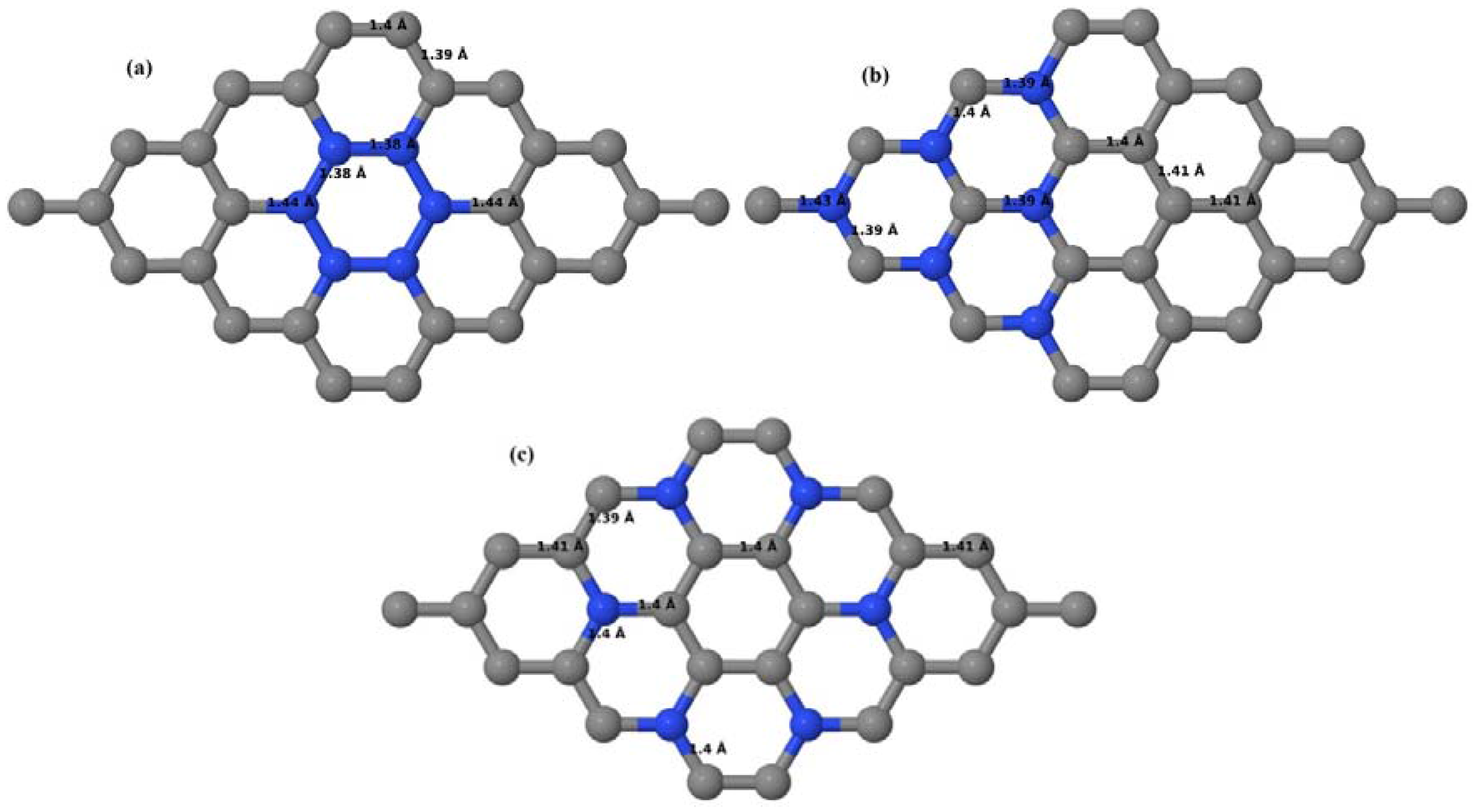
3.3.2. N-Doped Graphene System with Two N Atoms per Supercell
Here the substitution of two C atoms by two N atoms in 2 × 2, 3 × 3, 4 × 4, and 6 × 6 graphene supercells (
Figure 18a–l) are considered. Similar to graphene systems doped with one N atom, the optimized structures of graphene systems doped with two N atoms preserve the planar geometry of PG (
Figure 18a–l) even after the introduction of two N atoms. The relaxed lattice constant decreases from 2.458 Å to 2.454 Å, 2.449 Å, 2.441 Å, and 2.422 Å for 6 × 6, 4 × 4, 3 × 3, and 2 × 2 graphene supercells doped with two N atoms (2.78%, 6.25%, 11.11%, 25% N concentrations), respectively, which shows a decrease in lattice constant with increasing N-doping concentration, similar to that observed for graphene systems doped with one N atom.
Figure 18a–l present the optimized geometries of the 2 × 2, 3 × 3, 4 × 4, and 6 × 6 graphene supercells doped with two N atoms, in which the same configurations taken for graphene systems doped with two B atoms are considered. Three doping configurations of 2 × 2, 3 × 3, 4 × 4, and 6 × 6 supercells doped with two N atoms (corresponding to 25%, 11.11%, 6.25%, and 2.78% B concentrations, respectively) are selected, with dopant atoms at adjacent, (
Figure 18a,d,g,j), same (
Figure 18b,e,h,k), and alternate sublattice points (
Figure 18c,f,i,l). In graphene systems doped with two N atoms, the C–N and C–C bond lengths were reduced significantly (
Figure 18a–l) as compared to graphene systems doped with one N atom for retaining the structure. After obtaining the stable geometries, the cohesive energies were calculated for all considered graphene systems doped with two N atoms and are listed in
Table 8.
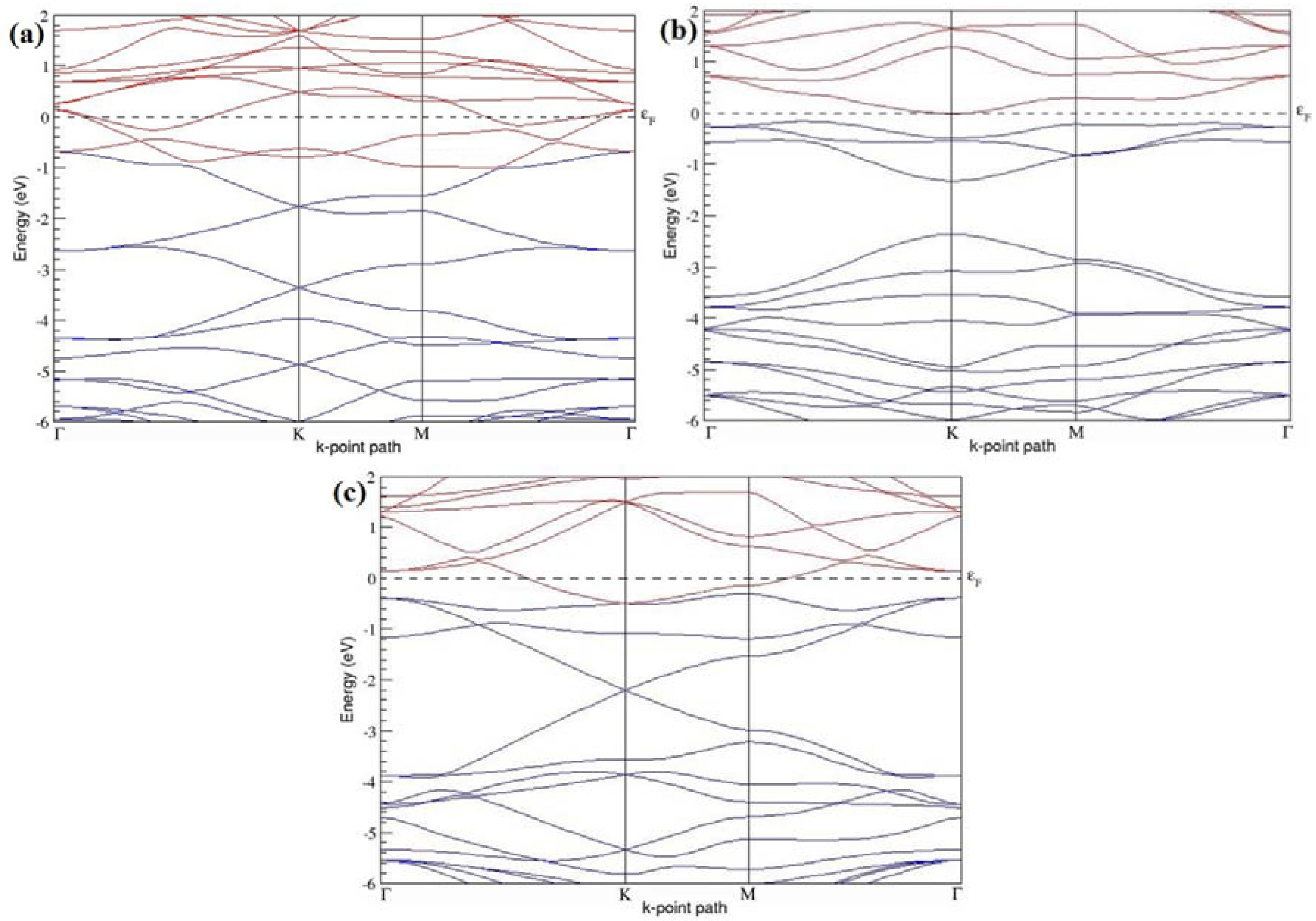
Figure 19a–l present the band structures computed for the optimized structures of different graphene systems doped with two N atoms shown in
Figure 18a–l. The band structures of 2 × 2, 3 × 3, and 4 × 4 graphene supercells doped with two N atoms are found to be in good agreement with those reported in [
43]. Similar to systems doped with two B atoms, the linear dispersion near the Dirac point is not completely destroyed (
Figure 19a–l), but an energy band gap opens in all cases except for the 2 × 2 graphene supercell doped with two N atoms at the alternate sublattice points (
Figure 19c). At a 25% N concentration, N-doped graphene has band gaps of 0.40 eV (
Figure 19a) and ~1.32 eV (
Figure 19b) upon placing the N atoms at adjacent and same sublattice positions in graphene, respectively. However, the band gap is found to be closed (
Figure 19c) for the configuration in which the N atoms are at alternate sublattices of a 2 × 2 graphene supercell, even though it corresponds to a high N-doping concentration of 25%.
In 4 × 4 graphene supercells doped with two N atoms (corresponding to 6.25% N concentration), band gaps of ~0.17 eV (
Figure 19g), ~0.40 eV (
Figure 19h), and ~0.01 eV (
Figure 19i) are observed for the configurations with N atoms at adjacent, same, and alternate sublattices, respectively. The large band gap opening in 2 × 2 and 4 × 4 graphene supercells doped with two N atoms, with the positioning of the dopant atoms at the same sublattice, is due to the combined effect of the symmetry breaking of sublattices, similar to that observed for graphene systems doped with two B atoms and are in accordance with that reported in [
30].
Similar to the 3 × 3 and 6 × 6 graphene supercells doped with two B atoms, the band structures of 3 × 3 and 6 × 6 graphene supercells doped with two N atoms are characterized by non-zero band gaps as shown in
Figure 19d–f,j–l. The 3 × 3 graphene supercell doped with two N atoms (corresponding to 11.11% N concentration) exhibit band gaps of ~0.25 eV (
Figure 19d), ~0.27 eV (
Figure 19e) and ~0.04 eV (
Figure 19f) for the configuration with N atoms at adjacent, same, and alternate sublattices, respectively. In N-doped graphene with 2.78% N concentration, band gaps of 0.085 eV (
Figure 19j), ~0.11 eV (
Figure 19k), and ~0.02 eV (
Figure 19l) appear when the dopants are at adjacent, same, and alternate sublattice sites in graphene.
All these systems doped with two N atoms in 2 × 2, 3 × 3, 4 × 4, and 6 × 6 graphene supercells exhibit
n-type metallic behavior. Our analysis of the electronic properties of the 2 × 2 and 4 × 4 graphene sheets doped with two N atoms are contrary to that of [
43].
Table 8 presents a summary of the considered N-doping concentrations with the doping configurations, the sublattices selected for the N atoms, the calculated cohesive energies, and the band gaps observed in each of these cases.
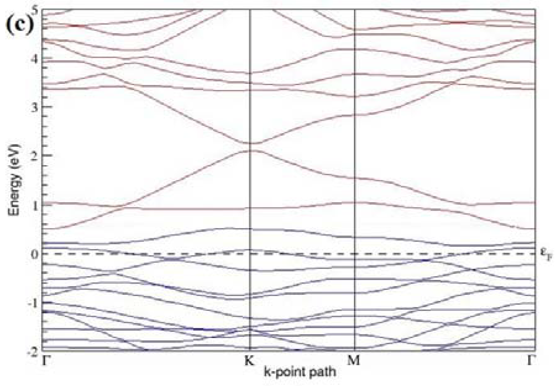
3.3.3. N-Doped Graphene System with Three N Atoms per Supercell
Here the substitutions of three C atoms by three N atoms are considered in 3 × 3 and 4 × 4 graphene supercells. All graphene systems doped with three N atoms have planar hexagonal structures as seen in
Figure 20a–f. The relaxed lattice constant decreases from 2.458 Å to 2.445 Å and 2.434 Å for 4 × 4 and 3 × 3 graphene supercells doped with three N atoms, (9.38% and 16.67% N concentrations), respectively, similar to that observed in graphene systems doped with one or two N atoms.
Figure 20a–f present the relaxed geometries of 3 × 3 and 4 × 4 graphene supercells doped with three N atoms, with N atoms at adjacent, same, and alternate sublattices, respectively. Compared with their B counterparts, graphene systems doped with three N atoms are found to have significantly less structural distortion, even when the three N atoms are placed at adjacent locations (
Figure 20a,d) due to the comparable size of C and N atoms.
Figure 21a–f present the band structures computed for the optimized structures of different graphene systems doped with three N atoms shown in
Figure 20a–f. Graphene systems doped with three N atoms in 3 × 3 and 4 × 4 graphene supercells exhibit
n-type metallic behavior with band gaps indicated in
Table 9. Similar to graphene systems doped with three B atoms, with dopants at adjacent positions, deformed band structures were obtained (
Figure 21a,d) for those structures in which the N-substitutional dopants are placed at the adjacent positions (
Figure 20a,d).
In 3 × 3 graphene systems doped with three N atoms (corresponding to 16.67% N concentration), a band gap of 0.93 eV (
Figure 21b) appears when the dopant atoms are placed at the same sublattices, whereas band gap values of ~0.29 eV (
Figure 21a) and 0.16 eV (
Figure 21c) appear when the dopant atoms are placed at the adjacent and alternate sublattice positions, respectively. The 4 × 4 graphene supercell doped with three N atoms (corresponding to 9.38% N concentration) induce band gaps of 0.27 eV (
Figure 21d), ~0.61 eV (
Figure 21e), and ~0.18 eV (
Figure 21f),for the configuration with N atoms at adjacent, same, and alternate sublattices, respectively.
Table 9 presents the doping concentrations, considered doping concentrations with sublattices, cohesive energies, and the band gaps introduced for all graphene systems doped with three N atoms.
3.3.4. N-Doped Graphene System with Four N Atoms per Supercell
Here we consider the substitution of four C atoms by four N atoms in 3 × 3 and 4 × 4 graphene supercells. After structural relaxation, all graphene systems doped with four N atoms appear to be planar by adjusting the adjoining bond lengths (
Figure 22a–f). The relaxed lattice constant decreases from 2.458 Å to 2.441 Å and 2.427 Å for 4 × 4 and 3 × 3 graphene supercells doped with four N atoms (corresponding to 12.5% and 22.22% N concentrations), respectively, which also indicates a decrease in lattice constant with the increase in N-doping concentration, as observed with other B-doped graphene systems.
Figure 22a–f present the relaxed structures of 3 × 3 and 4 × 4 supercells doped with four N atoms at adjacent, same, and alternate sublattices, respectively. As compared to graphene systems doped with four B atoms, graphene systems doped with four N atoms experience almost negligible structural distortion even upon placing the N atoms at the adjacent positions in the lattice (
Figure 22a,d).
Figure 23a–f present the band structures computed for the optimized structures of different graphene systems doped with four N atoms shown in
Figure 22a–f. Similar to graphene systems doped with three N atoms, all four N-doped graphene structures exhibit
n-type metallic properties with band gaps as seen in
Figure 23a–f. In 3 × 3 graphene systems doped with four N atoms (corresponding to 22.22%), the highest band gap value of ~0.80 eV (
Figure 23b) appears when the dopant atoms are placed at the same sublattices, whereas band gaps of 0.20 eV (
Figure 23a) and ~0.11 eV (
Figure 23c) are induced in graphene when the dopant atoms are placed at the adjacent positions and alternate sublattices, respectively. At a 12.5% N concentration, a maximum band gap of 0.70 eV (
Figure 23e) opens up when the dopant atoms are at the same sublattice, and a minimum band gap value of ~0.004 eV (
Figure 23f) appears when the dopant atoms are at alternate sublattice positions. The observed very small band gap for the doping configuration with N atoms at adjacent locations (
Figure 23d) corresponding to 12.5% N-doping concentration could be ascribed to the symmetry formed by the N dopants in the two triangular sublattices.
Table 10 presents the doping concentrations with selected sublattices, the cohesive energies, and the band gaps introduced for all graphene systems doped with four N atoms.
3.3.5. N-Doped Graphene System with Five N Atoms per Supercell
Here the substitution of five C atoms by five N atoms in a 4 × 4 graphene supercell are considered, with the dopant atoms at adjacent, same, and alternate sublattice positions. After structural relaxation, it was observed that all graphene systems doped with five N atoms exhibit planar geometry (
Figure 24a–c), similar to other N-doped graphene systems. The relaxed lattice constant decreases from 2.458 Å to 2.435 Å for the 4 × 4 graphene supercell doped with five N atoms (corresponding to 15.63% N concentration), as observed in other N-doped graphene systems. Similar to graphene systems doped with three N atoms, there is no structural distortion in the considered structures of graphene systems doped with five N atoms. The planar configuration is maintained by adjusting the associated bond lengths.
The band structures presented in
Figure 25a–c indicate that all graphene structures doped with five N atoms show an
n-type metallic character. At a 15.63% N concentration, N atoms located at adjacent, same, and alternate sublattices induce band gaps of ~0.36 eV (
Figure 25a), ~0.79 eV (
Figure 25b), and ~0.14 eV (
Figure 25c), respectively, in graphene as summarized in
Table 11.
Table 11 summarizes the observed band gaps and the calculated cohesive energies for different doping configurations corresponding to the 15.63% N concentration in graphene.
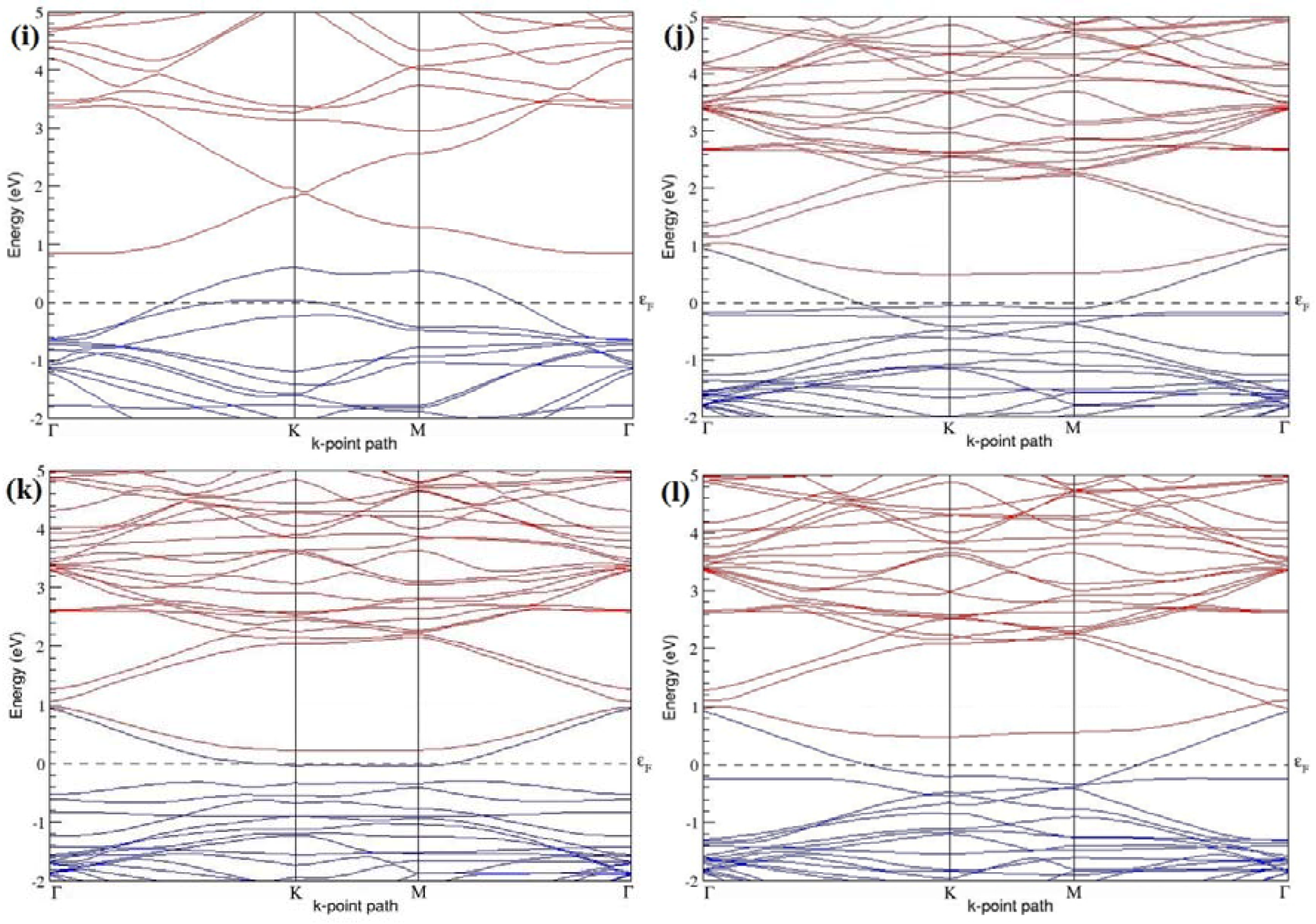
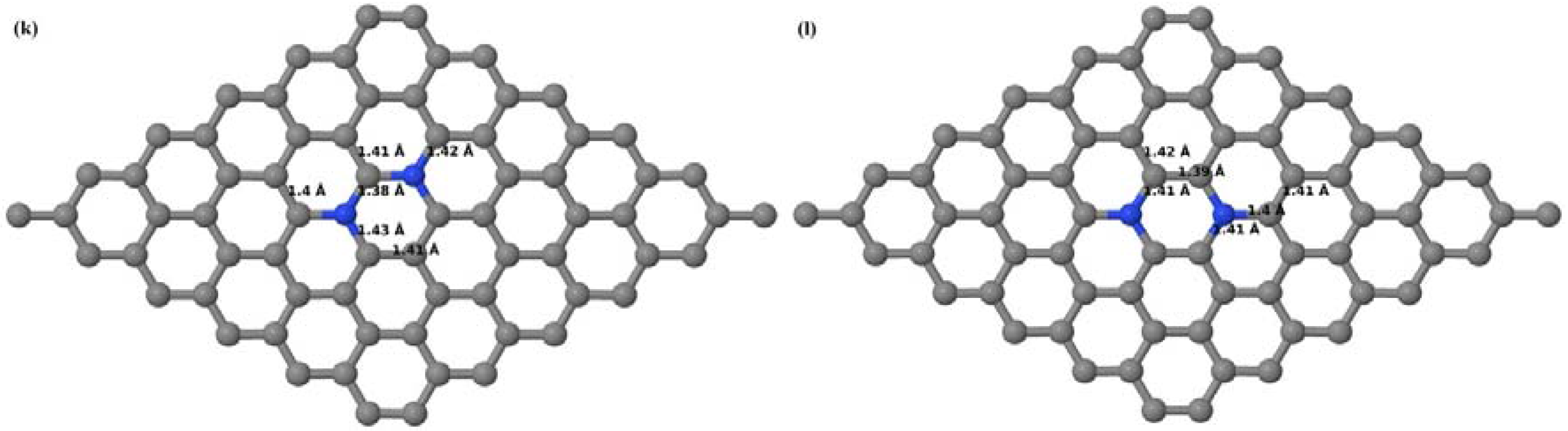
3.3.6. N-Doped Graphene System with Six N Atoms per Supercell
Here the substitutions of six C atoms by six N atoms are considered in the 4 × 4 graphene supercell with the dopant atoms at adjacent, same, and alternate sublattice positions. The planar structure is preserved even after the introduction of six N atoms in the lattice (
Figure 26a–c). The relaxed lattice constant decreases from 2.458 Å to 2.431 Å for 4 × 4 graphene supercell doped with six N atoms (corresponding to 18.75% N concentration), as observed in other N-doped graphene systems. Similar to other N-doped graphene systems, there is no geometrical distortion in the graphene systems doped with six N atoms.
All these 4 × 4 graphene systems doped with six N atoms show
n-type metallic behavior. At an 18.75% N concentration, a band gap of ~1.04 eV (
Figure 27b) opens up in graphene, when the six N atoms are located at the same sublattice sites of graphene. Upon placing the N atoms at adjacent and alternate sublattices, there is no band gap opening as evident from
Figure 27a,c, similar to that observed in graphene systems doped with six B atoms.
Table 12 summarizes the observed band gaps and the calculated cohesive energies for different doping configurations corresponding to the 18.75% N concentration in graphene.
4. Discussions
The changes in the bond lengths after B-doping can be read from the optimized structures shown in
Figure 3,
Figure 6,
Figure 8,
Figure 10,
Figure 12, and
Figure 14. In all B-doped graphene systems, the bond lengths are adjusted to retain the planar geometry, i.e., with long C–B bonds and relatively short adjacent C–C bonds based on the number and location of B atoms in graphene supercells. The placement of B atoms at adjacent locations results in large B–B bond lengths in B-doped graphene systems. The large B–B bond lengths observed for the configurations with B atoms at adjacent locations (
Figure 6a,d,g,j,
Figure 8a,d,
Figure 10a,d,
Figure 12a, and
Figure 14a could be ascribed to the large covalent radius of B compared to the host C atoms. The changes in the bond lengths after N-doping can be read from the optimized structures shown in
Figure 16,
Figure 18,
Figure 20,
Figure 22,
Figure 24, and
Figure 26. The planar configuration is also maintained in all N-doped graphene systems by adjusting the associated bond lengths, i.e., with short C–N and C–C bond lengths.
The obtained negative values of cohesive energies presented in
Table 1,
Table 2,
Table 3,
Table 4,
Table 5,
Table 6,
Table 7,
Table 8,
Table 9,
Table 10,
Table 11 and
Table 12 indicate that all considered B- and N-doped graphene systems are energetically stable. It was also observed that the cohesive energy increases with increase in B- and N-doping concentration (
Table 1,
Table 2,
Table 3,
Table 4,
Table 5,
Table 6,
Table 7,
Table 8,
Table 9,
Table 10,
Table 11 and
Table 12), which shows that energetic stability decreases with increasing B- and N-doping concentration. For the same doping concentration, the cohesive energy was found to be lowest for the doping configuration with dopants at an alternate sublattice and highest for the doping configuration with dopants at adjacent positions. These results show that B- and N-doped graphene with dopants placed at alternate sublattices are more stable than that with dopants placed at adjacent and same sublattice positions.
Table 1,
Table 2,
Table 3,
Table 4,
Table 5,
Table 6,
Table 7,
Table 8,
Table 9,
Table 10,
Table 11 and
Table 12 show that the band gap in general increases with the increase in the B- and N-doping concentration for the doping configuration with the highest band gap, which is in agreement with previous reports [
30]. Except in 3 × 3 and 6 × 6 graphene supercells doped with two B atoms, the band gap was found to be at a maximum when the B atoms were at the same sublattice and at a minimum when they were at adjacent or alternate sublattice positions, which is in agreement with report by Rani et al. [
30]. Even though 3 × 3 and 6 × 6 graphene supercells doped with two B atoms show a band gap between the valence and conduction bands, no specific dependence of the band gap on the B-atom positioning could be highlighted. Apart from the presented isomers of 3 × 3 and 6 × 6 graphene supercells doped with two B atoms (corresponding to 11.11% and 2.78% B concentrations), the band structures of several other isomers for the doping configurations of adjacent, same, and alternate sublattices are also calculated (which are not presented here) to check for the observed variation of band gap dependency on dopant positioning from that found in other B-doped graphene systems. The calculated band gaps in all cases of 3 × 3 and 6 × 6 graphene supercells doped with two B atoms do not follow any specific dependency on the B-doping configurations. The nature of this anomaly is still being investigated. On the other hand, 3 × 3 graphene supercells doped with three and four B or N atoms showed the highest band gap for the doping configurations with dopant atoms at same sublattices and the lowest band gap for the doping configuration with dopant atoms at alternate sublattices or adjacent positions. The trend of the band gap dependency on the doping configurations in all N-doped graphene systems was observed to be similar to that observed in corresponding B-doped graphene systems. Similar to the exception observed in the case of the 3 × 3 and 6 × 6 graphene supercells doped with two B atoms, no specific correlation between the band gap and the doping configuration could be determined for 3 × 3 and 6 × 6 graphene supercells doped with two N atoms (corresponding to 11.11% and 2.78% N concentrations). The band gaps of 2 × 2 graphene supercell doped with two N atoms (1.323 eV at a 25% N concentration) and 4 × 4 graphene supercell doped with six N atoms (1.042 eV at an 18.75% N concentration) are found to be very close to the band gap of silicon (1.1 eV).
The observed band gaps for the considered B or N concentrations corresponding to the most stable configurations are summarized in
Table 13. For the most probable configuration corresponding to the doping concentrations ranging from 2.78% to 22.22%, the observed band gaps lie within the range of 0.008–0.190 eV and 0.004–0.202 eV in B- and N-doped systems, respectively, while the most stable configuration corresponding to B or N concentrations of 1.39%, 5.56%, 18.75%, and 25% do not show a band gap. Thus, the band gap of graphene could be tailored from 0.008 eV to 0.190 eV by B-doping and from 0.004 eV to 0.202 eV by N-doping, within the concentration range of 2.78%–22.22%, excluding 5.56% and 18.75% concentrations.
As 2 × 2 graphene supercells doped with one B atom or one N atom and 4 × 4 graphene supercells doped with four B atoms or four N atoms correspond to the same doping concentration of 12.5%, the cohesive energies and electronic band structures of three different configurations of the 4 × 4 graphene sheet doped with four B atoms or four N atoms were compared with those of the 2 × 2 graphene sheet doped with one B atom or one N atom. The widths of the band gaps for a 12.5% doping concentration simulated by a 2 × 2 graphene supercell doped with one B atom or one N atom and a 4 × 4 graphene supercell doped with four B atoms or four N atoms were found to be almost the same only for the configuration of a 4 × 4 graphene supercell doped with four B atoms or four N atoms at the same sublattice. The band gaps introduced for other configurations of the 4 × 4 graphene supercell doped with four B atoms or four N atoms (adjacent and alternate sublattice positions) were observed to be comparatively small. However, the comparison of the cohesive energies of the 2 × 2 graphene sheet doped with one B atom or one N atom (−8.795 eV/atom and −9.029 eV/atom, respectively) and the 4 × 4 graphene supercell doped with four B atoms or four N atoms at the same sublattice (−8.829 eV/atom and −9.052 eV/atom, respectively) indicate that the cohesive energy is strongly dependent on the supercell size considered for the doping concentration. Thus, to achieve a 12.5% B or N doping concentration, the 4 × 4 graphene supercell doped with four B atoms or four N atoms is more stable than the 2 × 2 graphene supercell doped with one B atom or one N atom.
5. Conclusions
We have here calculated the energetic stabilities and the structural and electronic properties of B- and N-doped graphene with varying doping concentrations and several doping configurations in different graphene supercell sizes, using first-principles density functional theory calculations. It was observed that both B- and N-doped graphene maintain the planar geometry of pristine graphene with a slight distortion with longer C–B bonds and shorter C–N bonds compared to the C–C bond length, which is in agreement with previous reports. The doped structures with dopant atoms placed at adjacent locations have been found to be highly distorted, with less distortion in N-doped graphene systems compared to that of the corresponding B-doped graphene systems.
The stability was found to be decreasing with increases in B- and N-doping concentrations. For a particular doping concentration, stability was found to be higher for the atomic configuration with dopant atoms at alternate sublattice positions than other configurations and decreases in the order of alternate > same > adjacent. The cohesive energies of the N-doped graphene systems were found to be lower than that of similar B-doped graphene systems; hence, N-doped graphene structures are considered to be more stable than their B-doped counterparts. As the doping concentration decreases, the cohesive energy difference between similar N- and B-doped graphene structures also decrease, which indicates that graphene structures with a light doping of B and N atoms are highly stable.
All B-doped graphene systems exhibit p-type doping electronic properties as the Fermi level moves into the valence band, whereas all N-doped graphene systems exhibit n-type doping electronic properties as the Fermi level moves into the conduction band. The results also show that graphene with one B- and N-atom doping in any size of supercell exhibits p-type semiconducting and n-type metallic characters, respectively, with or without band gaps based on the doping concentration. The analysis of the electronic structures of 3 × 3 and 6 × 6 graphene supercells with more than one B or N atoms have shown non-zero band gaps around the Dirac point, different from the zero band gap observed for 3 × 3 and 6 × 6 graphene supercells doped with one B atom or one N atom. It was also observed that, for the same B- and N-doping concentration, the distribution of the dopant atoms in the crystal lattice determines the width of the introduced band gap around the Dirac point and affects the electronic band structures. The calculations show that B- and N-doped graphene systems with more than one dopant atom exhibit p-type semiconducting and n-type metallic behavior, respectively, with or without band gaps based on the doping concentrations and doping configurations.
Except in 3 × 3 and 6 × 6 graphene supercells with two B and N dopants (corresponding to 11.11% and 2.87% B and N doping concentrations, respectively), the band gap dependency on the dopant sites was observed to be the same, where a maximum band gap opens up when the dopant atoms are at the same sublattice and a minimum band gap opens up when the dopants are at alternate sublattices. No conceivable correlation between the band gap and the doping configurations could be deduced from the band structures of graphene doped with two B atoms and two N atoms in 3 × 3 and 6 × 6 graphene supercells. The 3 × 3 graphene supercells doped with three B atoms, three N atoms, four B atoms, or four N atoms show similar band gap dependency on the dopant locations that has been observed with other supercells which are not multiples of three.
Our calculations indicate that band gap can be adjusted as required based on the doping concentration and the doping configuration, which is of great significance in designing graphene-based semiconductor devices.


