

Recent Advances in Electronic and Optoelectronic Devices Based on Two-Dimensional Transition Metal Dichalcogenides


Abstract
1. Introduction
2. Field Effect Transistors
2.1. Transistors with Multilayered TMDCs
2.2. Transistors with Monolayer TMDCs
2.3. Ambipolar Transistors with TMDCs
2.4. Transistors with Vertical Hetero-Structures
3. Optoelectronic Devices
3.1. Solar Cells
3.2. Light-Emitting Diodes
3.3. Photodetectors
3.4. Lasers
4. Integrated Circuits
4.1. Amplifiers and Inverters
4.2. Logic Circuits
4.3. Memory Devices
5. Summary
Acknowledgments
Author Contributions
Conflicts of Interest
References
- Lundstrom, M. Applied physics. Moore’s law forever? Science 2003, 299, 210–211. [Google Scholar] [CrossRef] [Scilit] [PubMed]
- Theis, T.N.; Solomon, P.M. It’s time to reinvent the transistor! Science 2010, 327, 1600–1601. [Google Scholar] [CrossRef] [Scilit] [PubMed]
- Morton, J.J.; McCamey, D.R.; Eriksson, M.A.; Lyon, S.A. Embracing the quantum limit in silicon computing. Nature 2011, 479, 345–353. [Google Scholar] [CrossRef] [Scilit] [PubMed]
- Ferain, I.; Colinge, C.A.; Colinge, J.P. Multigate transistors as the future of classical metal-oxide-semiconductor field-effect transistors. Nature 2011, 479, 310–316. [Google Scholar] [CrossRef] [Scilit] [PubMed]
- Ionescu, A.M.; Riel, H. Tunnel field-effect transistors as energy-efficient electronic switches. Nature 2011, 479, 329–337. [Google Scholar] [CrossRef] [Scilit] [PubMed]
- Lee, C.H.; Qin, S.; Savaikar, M.A.; Wang, J.; Hao, B.; Zhang, D.; Banyai, D.; Jaszczak, J.A.; Clark, K.W.; Idrobo, J.C.; et al. Room-Temperature Tunneling Behavior of Boron Nitride Nanotubes Functionalized with Gold Quantum Dots. Adv. Mater. 2013, 25, 4544–4548. [Google Scholar] [CrossRef] [Scilit] [PubMed]
- Hao, B.; Asthana, A.; Hazaveh, P.K.; Bergstrom, P.L.; Banyai, D.; Savaikar, M.A.; Jaszczak, J.A.; Yap, Y.K. New Flexible Channels for Room Temperature Tunneling Field Effect Transistors. Sci. Rep. 2016, 6. [Google Scholar] [CrossRef] [Scilit] [PubMed]
- Parashar, V.; Durand, C.P.; Hao, B.; Amorim, R.G.; Pandey, R.; Tiwari, B.; Zhang, D.; Liu, Y.; Li, A.P.; Yap, Y.K. Switching Behaviors of Graphene-Boron Nitride Nanotube Heterojunctions. Sci. Rep. 2015, 5, 12238. [Google Scholar] [CrossRef] [Scilit] [PubMed]
- Shim, J.; Park, H.-Y.; Kang, D.-H.; Kim, J.-O.; Jo, S.-H.; Park, Y.; Park, J.-H. Electronic and Optoelectronic Devices based on Two-Dimensional Materials: From Fabrication to Application. Adv. Electron. Mater. 2017, 3, 1600364. [Google Scholar] [CrossRef] [Scilit]
- Ye, M.; Winslow, D.; Zhang, D.; Pandey, R.; Yap, Y. Recent Advancement on the Optical Properties of Two-Dimensional Molybdenum Disulfide (MoS2) Thin Films. Photonics 2015, 2, 288–307. [Google Scholar] [CrossRef] [Scilit]
- Tongay, S.; Zhou, J.; Ataca, C.; Lo, K.; Matthews, T.S.; Li, J.; Grossman, J.C.; Wu, J. Thermally driven crossover from indirect toward direct bandgap in 2D semiconductors: MoSe2 versus MoS2. Nano Lett. 2012, 12, 5576–5580. [Google Scholar] [CrossRef] [Scilit] [PubMed]
- Zhang, Y.; Chang, T.R.; Zhou, B.; Cui, Y.T.; Yan, H.; Liu, Z.; Schmitt, F.; Lee, J.; Moore, R.; Chen, Y.; et al. Direct observation of the transition from indirect to direct bandgap in atomically thin epitaxial MoSe2. Nat. Nanotechnol. 2014, 9, 111–115. [Google Scholar] [CrossRef] [Scilit] [PubMed]
- Goldberg, A.M.; Beal, A.R.; Lévy, F.A.; Davis, E.A. The low-energy absorption edge in 2H-MoS2 and 2H-MoSe2. Philos. Mag. 1975, 32, 367–378. [Google Scholar] [CrossRef] [Scilit]
- Coehoorn, R.; Haas, C.; Dijkstra, J.; Flipse, C.J.; de Groot, R.A.; Wold, A. Electronic structure of MoSe2, MoS2, and WSe2. I. Band-structure calculations and photoelectron spectroscopy. Phys. Rev. B Condens. Matter 1987, 35, 6195–6202. [Google Scholar] [CrossRef] [Scilit] [PubMed]
- Ma, Y.; Dai, Y.; Guo, M.; Niu, C.; Lu, J.; Huang, B. Electronic and magnetic properties of perfect, vacancy-doped, and nonmetal adsorbed MoSe2, MoTe2 and WS2 monolayers. Phys. Chem. Chem. Phys. 2011, 13, 15546–15553. [Google Scholar] [CrossRef] [Scilit] [PubMed]
- Ruppert, C.; Aslan, O.B.; Heinz, T.F. Optical properties and band gap of single- and few-layer MoTe2 crystals. Nano Lett. 2014, 14, 6231–6236. [Google Scholar] [CrossRef] [Scilit] [PubMed]
- Grant, A.J.; Griffiths, T.M.; Pitt, G.D.; Yoffe, A.D. The electrical properties and the magnitude of the indirect gap in the semiconducting transition metal dichalcogenide layer crystals. J. Phys. C Solid State Phys. 1975, 8, L17–L23. [Google Scholar] [CrossRef] [Scilit]
- Hind, S.P.; Lee, P.M. KKR calculations of the energy bands in NbSe2, MoS2 and alpha MoTe2. J. Phys. C Solid State Phys. 1980, 13, 349–357. [Google Scholar] [CrossRef] [Scilit]
- Ding, Y.; Wang, Y.; Ni, J.; Shi, L.; Shi, S.; Tang, W. First principles study of structural, vibrational and electronic properties of graphene-like MX2 (M = Mo, Nb, W, Ta; X = S, Se, Te) monolayers. Phys. B Condens. Matter 2011, 406, 2254–2260. [Google Scholar] [CrossRef] [Scilit]
- Jo, S.; Ubrig, N.; Berger, H.; Kuzmenko, A.B.; Morpurgo, A.F. Mono- and bilayer WS2 light-emitting transistors. Nano Lett. 2014, 14, 2019–2025. [Google Scholar] [CrossRef] [Scilit] [PubMed]
- Kam, K.K.; Parklnclon, B.A. Detailed Photocurrent Spectroscopy of the Semiconducting Grouping VI Transition Metal Dichalcogenides. J. Phys. Chem. 1982, 86, 463–467. [Google Scholar] [CrossRef] [Scilit]
- Zhao, W.; Ghorannevis, Z.; Chu, L.; Toh, M.; Kloc, C.; Tan, P.-H.; Eda, G. Evolution of Electronic Structure in Atomically Thin sheets of WS2 and WSe2. ACS Nano 2013, 7, 791–797. [Google Scholar] [CrossRef] [Scilit] [PubMed]
- Dawson, W.G.; Bullett, D.W. Electronic-Structure and Crystallography of MoTe2 and Wte2. J. Phys. C Solid State Phys. 1987, 20, 6159–6174. [Google Scholar] [CrossRef] [Scilit]
- Tongay, S.; Sahin, H.; Ko, C.; Luce, A.; Fan, W.; Liu, K.; Zhou, J.; Huang, Y.S.; Ho, C.H.; Yan, J.; et al. Monolayer behaviour in bulk ReS2 due to electronic and vibrational decoupling. Nat. Commun. 2014, 5, 3252. [Google Scholar] [CrossRef] [Scilit] [PubMed]
- Friemelt, K.; Kulikova, L.; Kulyuk, L.; Siminel, A.; Arushanov, E.; Kloc, C.; Bucher, E. Optical and photoelectrical properties of ReS2 single crystals. J. Appl. Phys. 1996, 79, 9268–9272. [Google Scholar] [CrossRef] [Scilit]
- Wolverson, D.; Crampin, S.; Kazemi, A.S.; Ilie, A.; Bending, S.J. Raman Spectra of Monolayer, Few-Layer, and Bulk ReSe2: An Anisotropic Layered Semiconductor. ACS Nano 2014, 8, 11154–11164. [Google Scholar] [CrossRef] [Scilit] [PubMed]
- Yang, S.; Tongay, S.; Li, Y.; Yue, Q.; Xia, J.B.; Li, S.S.; Li, J.; Wei, S.H. Layer-dependent electrical and optoelectronic responses of ReSe2 nanosheet transistors. Nanoscale 2014, 6, 7226–7231. [Google Scholar] [CrossRef] [Scilit] [PubMed]
- Yang, S.; Wang, C.; Sahin, H.; Chen, H.; Li, Y.; Li, S.S.; Suslu, A.; Peeters, F.M.; Liu, Q.; Li, J.; et al. Tuning the optical, magnetic, and electrical properties of ReSe2 by nanoscale strain engineering. Nano Lett. 2015, 15, 1660–1666. [Google Scholar] [CrossRef] [Scilit] [PubMed]
- Zhao, H.; Wu, J.B.; Zhong, H.X.; Guo, Q.S.; Wang, X.M.; Xia, F.N.; Yang, L.; Tan, P.H.; Wang, H. Interlayer interactions in anisotropic atomically thin rhenium diselenide. Nano Res. 2015, 8, 3651–3661. [Google Scholar] [CrossRef] [Scilit]
- Marzik, J.V.; Kershaw, R.; Dwight, K.; Wold, A. Photoelectronic properties of ReS2 and ReSe2 single crystals. J. Solid State Chem. 1984, 51, 170–175. [Google Scholar] [CrossRef] [Scilit]
- Ridley, B.K. The electron-phonon interaction in quasi-two-dimensional semiconductor quantum-well structures. J. Phys. C Solid State Phys. 1982, 15, 5899–5917. [Google Scholar] [CrossRef] [Scilit]
- Chen, J.H.; Jang, C.; Xiao, S.; Ishigami, M.; Fuhrer, M.S. Intrinsic and extrinsic performance limits of graphene devices on SiO2. Nat. Nanotechnol. 2008, 3, 206–209. [Google Scholar] [CrossRef] [Scilit] [PubMed]
- Fivaz, R.; Mooser, E. Mobility of Charge Carriers in Semiconducting Layer Structures. Phys. Rev. 1967, 163, 743–755. [Google Scholar] [CrossRef] [Scilit]
- Ando, T.; Fowler, A.B.; Stern, F. Electronic properties of two-dimensional systems. Rev. Mod. Phys. 1982, 54, 437–672. [Google Scholar] [CrossRef] [Scilit]
- Hwang, E.H.; Adam, S.; Sarma, S.D. Carrier transport in two-dimensional graphene layers. Phys. Rev. Lett. 2007, 98, 186806. [Google Scholar] [CrossRef] [Scilit] [PubMed]
- Hess, K.; Vogl, P. Remote polar phonon scattering in silicon inversion layers. Solid State Commun. 1979, 30, 797–799. [Google Scholar] [CrossRef] [Scilit]
- Nomura, K.; MacDonald, A.H. Quantum transport of massless Dirac fermions. Phys. Rev. Lett. 2007, 98, 076602. [Google Scholar] [CrossRef] [Scilit] [PubMed]
- Adam, S.; Hwang, E.H.; Sarma, S.D. Scattering mechanisms and Boltzmann transport in graphene. Phys. E Low-Dimens. Syst. Nanostruct. 2008, 40, 1022–1025. [Google Scholar] [CrossRef] [Scilit]
- Paul, T.; Ghatak, S.; Ghosh, A. Percolative switching in transition metal dichalcogenide field-effect transistors at room temperature. Nanotechnology 2016, 27, 125706. [Google Scholar] [CrossRef] [Scilit] [PubMed]
- Podzorov, V.; Gershenson, M.E.; Kloc, C.; Zeis, R.; Bucher, E. High-mobility field-effect transistors based on transition metal dichalcogenides. Appl. Phys. Lett. 2004, 84, 3301–3303. [Google Scholar] [CrossRef] [Scilit]
- Novoselov, K.S.; Jiang, D.; Schedin, F.; Booth, T.J.; Khotkevich, V.V.; Morozov, S.V.; Geim, A.K. Two-dimensional atomic crystals. Proc. Natl. Acad. Sci. USA 2005, 102, 10451–10453. [Google Scholar] [CrossRef] [Scilit] [PubMed]
- Ayari, A.; Cobas, E.; Ogundadegbe, O.; Fuhrer, M.S. Realization and electrical characterization of ultrathin crystals of layered transition-metal dichalcogenides. J. Appl. Phys. 2007, 101, 014507. [Google Scholar] [CrossRef] [Scilit]
- Lee, K.; Kim, H.Y.; Lotya, M.; Coleman, J.N.; Kim, G.T.; Duesberg, G.S. Electrical characteristics of molybdenum disulfide flakes produced by liquid exfoliation. Adv. Mater. 2011, 23, 4178–4182. [Google Scholar] [CrossRef] [Scilit] [PubMed]
- Zhu, W.J.; Perebeinos, V.; Freitag, M.; Avouris, P. Carrier scattering, mobilities, and electrostatic potential in monolayer, bilayer, and trilayer graphene. Phys. Rev. B 2009, 80, 235402. [Google Scholar] [CrossRef] [Scilit]
- Lee, Y.H.; Zhang, X.Q.; Zhang, W.; Chang, M.T.; Lin, C.T.; Chang, K.D.; Yu, Y.C.; Wang, J.T.; Chang, C.S.; Li, L.J.; et al. Synthesis of large-area MoS2 atomic layers with chemical vapor deposition. Adv. Mater. 2012, 24, 2320–2325. [Google Scholar] [CrossRef] [Scilit] [PubMed]
- Kim, S.; Konar, A.; Hwang, W.S.; Lee, J.H.; Lee, J.; Yang, J.; Jung, C.; Kim, H.; Yoo, J.B.; Choi, J.Y.; et al. High-mobility and low-power thin-film transistors based on multilayer MoS2 crystals. Nat. Commun. 2012, 3, 1011. [Google Scholar] [CrossRef] [Scilit] [PubMed]
- Qiu, H.; Pan, L.J.; Yao, Z.N.; Li, J.J.; Shi, Y.; Wang, X.R. Electrical characterization of back-gated bi-layer MoS2 field-effect transistors and the effect of ambient on their performances. Appl. Phys. Lett. 2012, 100, 123104. [Google Scholar]
- Liu, H.; Ye, P.D. MoS2 Dual-Gate MOSFET With Atomic-Layer-Deposited Al2O3 as Top-Gate Dielectric. IEEE Electron. Device Lett. 2012, 33, 546–548. [Google Scholar] [CrossRef] [Scilit]
- Das, S.; Chen, H.Y.; Penumatcha, A.V.; Appenzeller, J. High performance multilayer MoS2 transistors with scandium contacts. Nano Lett. 2013, 13, 100–105. [Google Scholar] [CrossRef] [Scilit] [PubMed]
- Wu, W.; De, D.; Chang, S.C.; Wang, Y.; Peng, H.; Bao, J.; Pei, S.-S. High mobility and high on/off ratio field-effect transistors based on chemical vapor deposited single-crystal MoS2 grains. Appl. Phys. Lett. 2013, 102, 142106. [Google Scholar] [CrossRef] [Scilit]
- Pradhan, N.R.; Rhodes, D.; Zhang, Q.; Talapatra, S.; Terrones, M.; Ajayan, P.M.; Balicas, L. Intrinsic carrier mobility of multi-layered MoS2 field-effect transistors on SiO2. Appl. Phys. Lett. 2013, 102, 123105. [Google Scholar] [CrossRef] [Scilit]
- Bao, W.Z.; Cai, X.H.; Kim, D.; Sridhara, K.; Fuhrer, M.S. High mobility ambipolar MoS2 field-effect transistors: Substrate and dielectric effects. Appl. Phys. Lett. 2013, 102, 042104. [Google Scholar] [CrossRef] [Scilit]
- Desai, S.B.; Madhvapathy, S.R.; Sachid, A.B.; Llinas, J.P.; Wang, Q.; Ahn, G.H.; Pitner, G.; Kim, M.J.; Bokor, J.; Hu, C.; Wong, H.S.P.; Javey, A. MoS2 transistors with 1-nanometer gate lengths. Science 2016, 354, 99–102. [Google Scholar] [CrossRef] [Scilit] [PubMed]
- Larentis, S.; Fallahazad, B.; Tutuc, E. Field-effect transistors and intrinsic mobility in ultra-thin MoSe2 layers. Appl. Phys. Lett. 2012, 101, 223104. [Google Scholar] [CrossRef] [Scilit]
- Chamlagain, B.; Li, Q.; Ghimire, N.J.; Chuang, H.J.; Perera, M.M.; Tu, H.; Xu, Y.; Pan, M.; Xiao, D.; Yan, J.; Mandrus, D.; Zhou, Z. Mobility improvement and temperature dependence in MoSe2 field-effect transistors on parylene-C substrate. ACS Nano 2014, 8, 5079–5088. [Google Scholar] [CrossRef] [Scilit] [PubMed]
- Pradhan, N.R.; Rhodes, D.; Xin, Y.; Memaran, S.; Bhaskaran, L.; Siddiq, M.; Hill, S.; Ajayan, P.M.; Balicas, L. Ambipolar molybdenum diselenide field-effect transistors: Field-effect and Hall mobilities. ACS Nano 2014, 8, 7923–7929. [Google Scholar] [CrossRef] [Scilit] [PubMed]
- Jung, C.; Kim, S.M.; Moon, H.; Han, G.; Kwon, J.; Hong, Y.K.; Omkaram, I.; Yoon, Y.; Kim, S.; Park, J. Highly Crystalline CVD-grown Multilayer MoSe2 Thin Film Transistor for Fast Photodetector. Sci. Rep. 2015, 5, 15313. [Google Scholar] [CrossRef] [Scilit] [PubMed]
- Lin, Y.F.; Xu, Y.; Wang, S.T.; Li, S.L.; Yamamoto, M.; Aparecido-Ferreira, A.; Li, W.; Sun, H.; Nakaharai, S.; Jian, W.B.; Ueno, K.; Tsukagoshi, K. Ambipolar MoTe2 transistors and their applications in logic circuits. Adv. Mater. 2014, 26, 3263–3269. [Google Scholar] [CrossRef] [Scilit] [PubMed]
- Pradhan, N.R.; Rhodes, D.; Feng, S.; Xin, Y.; Memaran, S.; Moon, B.H.; Terrones, H.; Terrones, M.; Balicas, L. Field-Effect Transistors Based on Few-Layered alpha-MoTe2. ACS Nano 2014, 8, 5911–5920. [Google Scholar] [CrossRef] [Scilit] [PubMed]
- Lezama, I.G.; Ubaldini, A.; Longobardi, M.; Giannini, E.; Renner, C.; Kuzmenko, A.B.; Morpurgo, A.F. Surface transport and band gap structure of exfoliated 2H-MoTe2 crystals. 2D Mater. 2014, 1, 021002. [Google Scholar] [CrossRef] [Scilit]
- Fathipour, S.; Ma, N.; Hwang, W.S.; Protasenko, V.; Vishwanath, S.; Xing, H.G.; Xu, H.; Jena, D.; Appenzeller, J.; Seabaugh, A. Exfoliated multilayer MoTe2 field-effect transistors. Appl. Phys. Lett. 2014, 105, 192101. [Google Scholar] [CrossRef] [Scilit]
- Xu, H.L.; Fathipour, S.; Kinder, E.W.; Seabaugh, A.C.; Fullerton-Shirey, S.K. Reconfigurable Ion Gating of 2H-MoTe2 Field-Effect Transistors Using Poly(ethylene oxide)-CsClO4 Solid Polymer Electrolyte. ACS Nano 2015, 9, 4900–4910. [Google Scholar] [CrossRef] [Scilit] [PubMed]
- Yin, L.; Zhan, X.Y.; Xu, K.; Wang, F.; Wang, Z.X.; Huang, Y.; Wang, Q.S.; Jiang, C.; He, J. Ultrahigh sensitive MoTe2 phototransistors driven by carrier tunneling. Appl. Phys. Lett. 2016, 108, 043503. [Google Scholar] [CrossRef] [Scilit]
- Octon, T.J.; Nagareddy, V.K.; Russo, S.; Craciun, M.F.; Wright, C.D. Fast High-Responsivity Few-Layer MoTe2 Photodetectors. Adv. Opt. Mater. 2016, 4, 1750–1754. [Google Scholar] [CrossRef] [Scilit]
- Sik Hwang, W.; Remskar, M.; Yan, R.; Protasenko, V.; Tahy, K.; Doo Chae, S.; Zhao, P.; Konar, A.; Xing, H.; Seabaugh, A.; et al. Transistors with chemically synthesized layered semiconductor WS2 exhibiting 105 room temperature modulation and ambipolar behavior. Appl. Phys. Lett. 2012, 101, 013107. [Google Scholar] [CrossRef] [Scilit]
- Braga, D.; Gutierrez Lezama, I.; Berger, H.; Morpurgo, A.F. Quantitative determination of the band gap of WS2 with ambipolar ionic liquid-gated transistors. Nano Lett. 2012, 12, 5218–5223. [Google Scholar] [CrossRef] [Scilit] [PubMed]
- Liu, X.; Hu, J.; Yue, C.; Della Fera, N.; Ling, Y.; Mao, Z.; Wei, J. High performance field-effect transistor based on multilayer tungsten disulfide. ACS Nano 2014, 8, 10396–10402. [Google Scholar] [CrossRef] [Scilit] [PubMed]
- Kumar, J.; Kuroda, M.A.; Bellus, M.Z.; Han, S.J.; Chiu, H.Y. Full-range electrical characteristics of WS2 transistors. Appl. Phys. Lett. 2015, 106, 123508. [Google Scholar] [CrossRef] [Scilit]
- Chuang, H.J.; Tan, X.; Ghimire, N.J.; Perera, M.M.; Chamlagain, B.; Cheng, M.M.; Yan, J.; Mandrus, D.; Tomanek, D.; Zhou, Z. High mobility WSe2 p- and n-type field-effect transistors contacted by highly doped graphene for low-resistance contacts. Nano Lett. 2014, 14, 3594–3601. [Google Scholar] [CrossRef] [Scilit] [PubMed]
- Zhou, H.; Wang, C.; Shaw, J.C.; Cheng, R.; Chen, Y.; Huang, X.; Liu, Y.; Weiss, N.O.; Lin, Z.; Huang, Y.; et al. Large area growth and electrical properties of p-type WSe2 atomic layers. Nano Lett. 2015, 15, 709–713. [Google Scholar] [CrossRef] [Scilit] [PubMed]
- Pradhan, N.R.; Rhodes, D.; Memaran, S.; Poumirol, J.M.; Smirnov, D.; Talapatra, S.; Feng, S.; Perea-Lopez, N.; Elias, A.L.; Terrones, M.; et al. Hall and field-effect mobilities in few layered p-WSe(2) field-effect transistors. Sci. Rep. 2015, 5, 8979. [Google Scholar] [CrossRef] [Scilit] [PubMed]
- Campbell, P.M.; Tarasov, A.; Joiner, C.A.; Tsai, M.Y.; Pavlidis, G.; Graham, S.; Ready, W.J.; Vogel, E.M. Field-effect transistors based on wafer-scale, highly uniform few-layer p-type WSe2. Nanoscale 2016, 8, 2268–2276. [Google Scholar] [CrossRef] [Scilit] [PubMed]
- Liu, B.; Ma, Y.; Zhang, A.; Chen, L.; Abbas, A.N.; Liu, Y.; Shen, C.; Wan, H.; Zhou, C. High-Performance WSe2 Field-Effect Transistors via Controlled Formation of In-Plane Heterojunctions. ACS Nano 2016, 10, 5153–5160. [Google Scholar] [CrossRef] [Scilit] [PubMed]
- Corbet, C.M.; McClellan, C.; Rai, A.; Sonde, S.S.; Tutuc, E.; Banerjee, S.K. Field effect transistors with current saturation and voltage gain in ultrathin ReS2. ACS Nano 2015, 9, 363–370. [Google Scholar] [CrossRef] [Scilit] [PubMed]
- Zhang, E.; Jin, Y.; Yuan, X.; Wang, W.; Zhang, C.; Tang, L.; Liu, S.; Zhou, P.; Hu, W.; Xiu, F. ReS2-Based Field-Effect Transistors and Photodetectors. Adv. Funct. Mater. 2015, 25, 4076–4082. [Google Scholar] [CrossRef] [Scilit]
- Liu, E.; Fu, Y.; Wang, Y.; Feng, Y.; Liu, H.; Wan, X.; Zhou, W.; Wang, B.; Shao, L.; Ho, C.H.; et al. Integrated digital inverters based on two-dimensional anisotropic ReS2 field-effect transistors. Nat. Commun. 2015, 6, 6991. [Google Scholar] [CrossRef] [Scilit] [PubMed]
- Xu, K.; Deng, H.X.; Wang, Z.; Huang, Y.; Wang, F.; Li, S.S.; Luo, J.W.; He, J. Sulfur vacancy activated field effect transistors based on ReS2 nanosheets. Nanoscale 2015, 7, 15757–15762. [Google Scholar] [CrossRef] [Scilit] [PubMed]
- Shim, J.; Oh, A.; Kang, D.H.; Oh, S.; Jang, S.K.; Jeon, J.; Jeon, M.H.; Kim, M.; Choi, C.; Lee, J.; et al. High-Performance 2D Rhenium Disulfide (ReS2) Transistors and Photodetectors by Oxygen Plasma Treatment. Adv. Mater. 2016, 28, 6985–6992. [Google Scholar] [CrossRef] [Scilit] [PubMed]
- Keyshar, K.; Gong, Y.; Ye, G.; Brunetto, G.; Zhou, W.; Cole, D.P.; Hackenberg, K.; He, Y.; Machado, L.; Kabbani, M.; et al. Chemical Vapor Deposition of Monolayer Rhenium Disulfide (ReS2). Adv. Mater. 2015, 27, 4640–4648. [Google Scholar] [CrossRef] [Scilit] [PubMed]
- Corbet, C.M.; Sonde, S.S.; Tutuc, E.; Banerjee, S.K. Improved contact resistance in ReSe2 thin film field-effect transistors. Appl. Phys. Lett. 2016, 108, 162104. [Google Scholar] [CrossRef] [Scilit]
- Hafeez, M.; Gan, L.; Li, H.; Ma, Y.; Zhai, T. Chemical Vapor Deposition Synthesis of Ultrathin Hexagonal ReSe2 Flakes for Anisotropic Raman Property and Optoelectronic Application. Adv. Mater. 2016, 28, 8296–8301. [Google Scholar] [CrossRef] [Scilit] [PubMed]
- Radisavljevic, B.; Radenovic, A.; Brivio, J.; Giacometti, V.; Kis, A. Single-layer MoS2 transistors. Nat. Nanotechnol. 2011, 6, 147–150. [Google Scholar] [CrossRef] [Scilit] [PubMed]
- Ghatak, S.; Pal, A.N.; Ghosh, A. Nature of Electronic States in Atomically Thin MoS2 Field-Effect Transistors. ACS Nano 2011, 5, 7707–7712. [Google Scholar] [CrossRef] [Scilit] [PubMed]
- Van der Zande, A.M.; Huang, P.Y.; Chenet, D.A.; Berkelbach, T.C.; You, Y.; Lee, G.H.; Heinz, T.F.; Reichman, D.R.; Muller, D.A.; Hone, J.C. Grains and grain boundaries in highly crystalline monolayer molybdenum disulphide. Nat. Mater. 2013, 12, 554–561. [Google Scholar] [CrossRef] [Scilit] [PubMed]
- Yazyev, O.V.; Louie, S.G. Electronic transport in polycrystalline graphene. Nat. Mater. 2010, 9, 806–809. [Google Scholar] [CrossRef] [Scilit] [PubMed]
- Hwang, S.W.; Remskar, M.; Yan, R.; Kosel, T.; Park, J.K.; Cho, B.J.; Haensch, W.; Xing, H.; Seabaugh, A.; Jena, D. Comparative study of chemically synthesized and exfoliated multilayer MoS2 field-effect transistors. Appl. Phys. Lett. 2013, 102, 043116. [Google Scholar] [CrossRef] [Scilit]
- Walia, S.; Balendhran, S.; Wang, Y.C.; Ab Kadir, R.; Zoolfakar, A.S.; Atkin, P.; Ou, J.Z.; Sriram, S.; Kalantar-zadeh, K.; Bhaskaran, M. Characterization of metal contacts for two-dimensional MoS2 nanoflakes. Appl. Phys. Lett. 2013, 103, 232105. [Google Scholar] [CrossRef] [Scilit]
- Strait, J.H.; Nene, P.; Rana, F. High intrinsic mobility and ultrafast carrier dynamics in multilayer metal-dichalcogenideMoS2. Phys. Rev. B 2014, 90, 245402. [Google Scholar] [CrossRef] [Scilit]
- Das, S.; Appenzeller, J. Where does the current flow in two-dimensional layered systems? Nano Lett. 2013, 13, 3396–3402. [Google Scholar] [CrossRef] [Scilit] [PubMed]
- Cheng, R.; Jiang, S.; Chen, Y.; Liu, Y.; Weiss, N.; Cheng, H.C.; Wu, H.; Huang, Y.; Duan, X. Few-layer molybdenum disulfide transistors and circuits for high-speed flexible electronics. Nat. Commun. 2014, 5, 5143. [Google Scholar] [CrossRef] [Scilit] [PubMed]
- Wang, H.; Yu, L.; Lee, Y.H.; Fang, W.; Hsu, A.; Herring, P.; Chin, M.; Dubey, M.; Li, L.J.; Kong, J.; et al. Large-scale 2D electronics based on single-layer MoS2 grown by chemical vapor deposition. IEDM Tech. Dig. 2012, 4.6.1–4.6.4. [Google Scholar] [CrossRef] [Scilit]
- Das, S.R.; Kwon, J.; Prakash, A.; Delker, C.J.; Das, S.; Janes, D.B. Low-frequency noise in MoSe2 field effect transistors. Appl. Phys. Lett. 2015, 106, 083507. [Google Scholar] [CrossRef] [Scilit]
- Kwon, H.-J.; Kang, H.; Jang, J.; Kim, S.; Grigoropoulos, C.P. Analysis of flicker noise in two-dimensional multilayer MoS2 transistors. Appl. Phys. Lett. 2014, 104, 083110. [Google Scholar] [CrossRef] [Scilit]
- Na, J.; Joo, M.K.; Shin, M.; Huh, J.; Kim, J.S.; Piao, M.; Jin, J.E.; Jang, H.K.; Choi, H.J.; Shim, J.H.; et al. Low-frequency noise in multilayer MoS2 field-effect transistors: the effect of high-k passivation. Nanoscale 2014, 6, 433–441. [Google Scholar] [CrossRef] [Scilit] [PubMed]
- Liu, L.; Kumar, S.B.; Ouyang, Y.; Guo, J. Performance Limits of Monolayer Transition Metal Dichalcogenide Transistors. IEEE Trans. Electron. Devices 2011, 58, 3042–3047. [Google Scholar] [CrossRef] [Scilit]
- Yoon, Y.; Ganapathi, K.; Salahuddin, S. How good can monolayer MoS2 transistors be? Nano Lett. 2011, 11, 3768–3773. [Google Scholar] [CrossRef] [Scilit] [PubMed]
- Radisavljevic, B.; Whitwick, M.B.; Kis, A. Integrated Circuits and Logic Operations Based on Single-Layer MoS2. ACS Nano 2011, 5, 9934–9938. [Google Scholar] [CrossRef] [Scilit] [PubMed]
- Zhan, Y.; Liu, Z.; Najmaei, S.; Ajayan, P.M.; Lou, J. Large-area vapor-phase growth and characterization of MoS2 atomic layers on a SiO2 substrate. Small 2012, 8, 966–971. [Google Scholar] [CrossRef] [Scilit] [PubMed]
- Late, D.J.; Liu, B.; Matte, H.S.; Dravid, V.P.; Rao, C.N. Hysteresis in single-layer MoS2 field effect transistors. ACS Nano 2012, 6, 5635–5641. [Google Scholar] [CrossRef] [Scilit] [PubMed]
- Lin, M.-W.; Liu, L.Z.; Lan, Q.; Tan, X.B.; Dhindsa, K.S.; Zeng, P.; Naik, V.M.; Cheng, M.M.C.; Zhou, Z.X. Mobility enhancement and highly efficient gating of monolayer MoS2transistors with polymer electrolyte. J. Phys. D Appl. Phys. 2012, 45, 345102. [Google Scholar] [CrossRef] [Scilit]
- Lee, H.S.; Min, S.W.; Park, M.K.; Lee, Y.T.; Jeon, P.J.; Kim, J.H.; Ryu, S.; Im, S. MoS2 nanosheets for top-gate nonvolatile memory transistor channel. Small 2012, 8, 3111–3115. [Google Scholar] [CrossRef] [Scilit] [PubMed]
- Radisavljevic, B.; Whitwick, M.B.; Kis, A. Small-signal amplifier based on single-layer MoS2. Appl. Phys. Lett. 2012, 101, 043103. [Google Scholar] [CrossRef] [Scilit]
- Lembke, D.; Kis, A. Breakdown of high-performance monolayer MoS2 transistors. ACS Nano 2012, 6, 10070–10075. [Google Scholar] [CrossRef] [Scilit] [PubMed]
- Baugher, B.W.; Churchill, H.O.; Yang, Y.; Jarillo-Herrero, P. Intrinsic electronic transport properties of high-quality monolayer and bilayer MoS2. Nano Lett. 2013, 13, 4212–4216. [Google Scholar] [CrossRef] [Scilit] [PubMed]
- Park, W.; Baik, J.; Kim, T.Y.; Cho, K.; Hong, W.K.; Shin, H.J.; Lee, T. Photoelectron spectroscopic imaging and device applications of large-area patternable single-layer MoS2 synthesized by chemical vapor deposition. ACS Nano 2014, 8, 4961–4968. [Google Scholar] [CrossRef] [Scilit] [PubMed]
- Sanne, A.; Ghosh, R.; Rai, A.; Movva, H.C.P.; Sharma, A.; Rao, R.; Mathew, L.; Banerjee, S.K. Top-gated chemical vapor deposited MoS2 field-effect transistors on Si3N4 substrates. Appl. Phys. Lett. 2015, 106, 062101. [Google Scholar] [CrossRef] [Scilit]
- Shao, P.-Z.; Zhao, H.M.; Cao, H.W.; Wang, X.F.; Pang, Y.; Li, Y.X.; Deng, N.Q.; Zhang, J.; Zhang, G.Y.; Yang, Y.; et al. Enhancement of carrier mobility in MoS2 field effect transistors by a SiO2 protective layer. Appl. Phys. Lett. 2016, 108, 203105. [Google Scholar] [CrossRef] [Scilit]
- Amani, M.; Chin, M.L.; Birdwell, A.G.; O’Regan, T.P.; Najmaei, S.; Liu, Z.; Ajayan, P.M.; Lou, J.; Dubey, M. Electrical performance of monolayer MoS2 field-effect transistors prepared by chemical vapor deposition. Appl. Phys. Lett. 2013, 102, 193107. [Google Scholar] [CrossRef] [Scilit]
- Lu, X.; Utama, M.I.; Lin, J.; Gong, X.; Zhang, J.; Zhao, Y.; Pantelides, S.T.; Wang, J.; Dong, Z.; Liu, Z.; et al. Large-area synthesis of monolayer and few-layer MoSe2 films on SiO2 substrates. Nano Lett. 2014, 14, 2419–2425. [Google Scholar] [CrossRef] [Scilit] [PubMed]
- Wang, X.; Gong, Y.; Shi, G.; Chow, W.L.; Keyshar, K.; Ye, G.; Vajtai, R.; Lou, J.; Liu, Z.; Ringe, E.; et al. Chemical vapor deposition growth of crystalline monolayer MoSe2. ACS Nano 2014, 8, 5125–5131. [Google Scholar] [CrossRef] [Scilit] [PubMed]
- Chang, Y.H.; Zhang, W.; Zhu, Y.; Han, Y.; Pu, J.; Chang, J.K.; Hsu, W.T.; Huang, J.K.; Hsu, C.L.; Chiu, M.H.; et al. Monolayer MoSe2 grown by chemical vapor deposition for fast photodetection. ACS Nano 2014, 8, 8582–8590. [Google Scholar] [CrossRef] [Scilit] [PubMed]
- Ovchinnikov, D.; Allain, A.; Huang, Y.S.; Dumcenco, D.; Kis, A. Electrical transport properties of single-layer WS2. ACS Nano 2014, 8, 8174–8181. [Google Scholar] [CrossRef] [Scilit] [PubMed]
- Xu, Z.Q.; Zhang, Y.; Lin, S.; Zheng, C.; Zhong, Y.L.; Xia, X.; Li, Z.; Sophia, P.J.; Fuhrer, M.S.; Cheng, Y.B.; et al. Synthesis and Transfer of Large-Area Monolayer WS2 Crystals: Moving Toward the Recyclable Use of Sapphire Substrates. ACS Nano 2015, 9, 6178–6187. [Google Scholar] [CrossRef] [Scilit] [PubMed]
- Hanbicki, A.T.; Currie, M.; Kioseoglou, G.; Friedman, A.L.; Jonker, B.T. Measurement of high exciton binding energy in the monolayer transition-metal dichalcogenides WS2 and WSe2. Solid State Commun. 2015, 203, 16–20. [Google Scholar] [CrossRef] [Scilit]
- Fang, H.; Chuang, S.; Chang, T.C.; Takei, K.; Takahashi, T.; Javey, A. High-performance single layered WSe(2) p-FETs with chemically doped contacts. Nano Lett. 2012, 12, 3788–3792. [Google Scholar] [CrossRef] [Scilit] [PubMed]
- Huang, J.K.; Pu, J.; Hsu, C.L.; Chiu, M.H.; Juang, Z.Y.; Chang, Y.H.; Chang, W.H.; Iwasa, Y.; Takenobu, T.; Li, L.J. Large-Area Synthesis of Highly Crystalline WSe2 Monolayers and Device Applications. ACS Nano 2014, 8, 923–930. [Google Scholar] [CrossRef] [Scilit] [PubMed]
- Allain, A.; Kis, A. Electron and hole mobilities in single-layer WSe2. ACS Nano 2014, 8, 7180–7185. [Google Scholar] [CrossRef] [Scilit] [PubMed]
- Kawamura, T.; Das Sarma, S. Temperature dependence of the low-temperature mobility in ultrapureAlxGa1−xAs/GaAs heterojunctions: Acoustic-phonon scattering. Phys. Rev. B 1990, 42, 3725–3728. [Google Scholar] [CrossRef] [Scilit]
- Hwang, E.H.; Das Sarma, S. Limit to two-dimensional mobility in modulation-doped GaAs quantum structures: How to achieve a mobility of 100 million. Phys. Rev. B 2008, 77, 235437. [Google Scholar] [CrossRef] [Scilit]
- Kaasbjerg, K.; Thygesen, K.S.; Jacobsen, K.W. Phonon-limited mobility in n-type single-layer MoS2 from first principles. Phys. Rev. B 2012, 85, 115317. [Google Scholar] [CrossRef] [Scilit]
- Zhang, W.X.; Huang, Z.S.; Zhang, W.L.; Li, Y.R. Two-dimensional semiconductors with possible high room temperature mobility. Nano Res. 2014, 7, 1731–1737. [Google Scholar] [CrossRef] [Scilit]
- Jena, D.; Konar, A. Enhancement of carrier mobility in semiconductor nanostructures by dielectric engineering. Phys. Rev. Lett. 2007, 98, 136805. [Google Scholar] [CrossRef] [Scilit] [PubMed]
- Chen, F.; Xia, J.; Ferry, D.K.; Tao, N. Dielectric screening enhanced performance in graphene FET. Nano Lett. 2009, 9, 2571–2574. [Google Scholar] [CrossRef] [Scilit] [PubMed]
- Konar, A.; Fang, T.; Jena, D. Effect of high-κgate dielectrics on charge transport in graphene-based field effect transistors. Phys. Rev. B 2010, 82, 115452. [Google Scholar] [CrossRef] [Scilit]
- Newaz, A.K.; Puzyrev, Y.S.; Wang, B.; Pantelides, S.T.; Bolotin, K.I. Probing charge scattering mechanisms in suspended graphene by varying its dielectric environment. Nat. Commun. 2012, 3, 734. [Google Scholar] [CrossRef] [Scilit] [PubMed]
- Radisavljevic, B.; Kis, A. Mobility engineering and a metal-insulator transition in monolayer MoS(2). Nat. Mater. 2013, 12, 815–820. [Google Scholar] [CrossRef] [Scilit] [PubMed]
- Sakaki, H.; Noda, T.; Hirakawa, K.; Tanaka, M.; Matsusue, T. Interface roughness scattering in GaAs/AlAs quantum wells. Appl. Phys. Lett. 1987, 51, 1934–1936. [Google Scholar] [CrossRef] [Scilit]
- Popov, I.; Seifert, G.; Tomanek, D. Designing electrical contacts to MoS2 monolayers: A computational study. Phys. Rev. Lett. 2012, 108, 156802. [Google Scholar] [CrossRef] [Scilit] [PubMed]
- Kang, J.H.; Liu, W.; Sarkar, D.; Jena, D.; Banerjee, K. Computational Study of Metal Contacts to Monolayer Transition-Metal Dichalcogenide Semiconductors. Phys. Rev. X 2014, 4, 031005. [Google Scholar] [CrossRef] [Scilit]
- Wang, Y.; Yang, R.X.; Quhe, R.; Zhong, H.; Cong, L.; Ye, M.; Ni, Z.; Song, Z.; Yang, J.; Shi, J.; et al. Does p-type ohmic contact exist in WSe2-metal interfaces? Nanoscale 2016, 8, 1179–1191. [Google Scholar] [CrossRef] [Scilit] [PubMed]
- Zhong, H.; Quhe, R.; Wang, Y.; Ni, Z.; Ye, M.; Song, Z.; Pan, Y.; Yang, J.; Yang, L.; Lei, M.; et al. Interfacial Properties of Monolayer and Bilayer MoS2 Contacts with Metals: Beyond the Energy Band Calculations. Sci. Rep. 2016, 6, 21786. [Google Scholar] [CrossRef] [Scilit] [PubMed]
- Gong, C.; Huang, C.; Miller, J.; Cheng, L.; Hao, Y.; Cobden, D.; Kim, J.; Ruoff, R.S.; Wallace, R.M.; Cho, K.; et al. Metal contacts on physical vapor deposited monolayer MoS2. ACS Nano 2013, 7, 11350–11357. [Google Scholar] [CrossRef] [Scilit] [PubMed]
- Leong, W.S.; Luo, X.; Li, Y.; Khoo, K.H.; Quek, S.Y.; Thong, J.T. Low resistance metal contacts to MoS2 devices with nickel-etched-graphene electrodes. ACS Nano 2015, 9, 869–877. [Google Scholar] [CrossRef] [Scilit] [PubMed]
- Farmanbar, M.; Brocks, G. Controlling the Schottky barrier at MoS2/metal contacts by inserting a BN monolayer. Phys. Rev. B 2015, 91, 161304. [Google Scholar] [CrossRef] [Scilit]
- Chuang, H.J.; Chamlagain, B.; Koehler, M.; Perera, M.M.; Yan, J.; Mandrus, D.; Tomanek, D.; Zhou, Z. Low-Resistance 2D/2D Ohmic Contacts: A Universal Approach to High-Performance WSe2, MoS2, and MoSe2 Transistors. Nano Lett. 2016, 16, 1896–1902. [Google Scholar] [CrossRef] [Scilit] [PubMed]
- Farmanbar, M.; Brocks, G. Ohmic Contacts to 2D Semiconductors through van der Waals Bonding. Adv. Electron. Mater. 2016, 2, 1500405. [Google Scholar] [CrossRef] [Scilit]
- Chen, J.R.; Odenthal, P.M.; Swartz, A.G.; Floyd, G.C.; Wen, H.; Luo, K.Y.; Kawakami, R.K. Control of Schottky barriers in single layer MoS2 transistors with ferromagnetic contacts. Nano Lett. 2013, 13, 3106–3110. [Google Scholar] [CrossRef] [Scilit] [PubMed]
- Dankert, A.; Langouche, L.; Kamalakar, M.V.; Dash, S.P. High-performance molybdenum disulfide field-effect transistors with spin tunnel contacts. ACS Nano 2014, 8, 476–482. [Google Scholar] [CrossRef] [Scilit] [PubMed]
- Kappera, R.; Voiry, D.; Yalcin, S.E.; Branch, B.; Gupta, G.; Mohite, A.D.; Chhowalla, M. Phase-engineered low-resistance contacts for ultrathin MoS2 transistors. Nat. Mater. 2014, 13, 1128–1134. [Google Scholar] [CrossRef] [Scilit] [PubMed]
- Kappera, R.; Voiry, D.; Yalcin, S.E.; Jen, W.; Acerce, M.; Torrel, S.; Branch, B.; Lei, S.D.; Chen, W.B.; Najmaei, S.; et al. Metallic 1T phase source/drain electrodes for field effect transistors from chemical vapor deposited MoS2. APL Mater. 2014, 2, 092516. [Google Scholar] [CrossRef] [Scilit]
- Cho, S.; Kim, S.; Kim, J.H.; Zhao, J.; Seok, J.; Keum, D.H.; Baik, J.; Choe, D.H.; Chang, K.J.; Suenaga, K.; et al. DEVICE TECHNOLOGY. Phase patterning for ohmic homojunction contact in MoTe2. Science 2015, 349, 625–628. [Google Scholar] [CrossRef] [Scilit] [PubMed]
- Ma, Y.; Liu, B.; Zhang, A.; Chen, L.; Fathi, M.; Shen, C.; Abbas, A.N.; Ge, M.; Mecklenburg, M.; Zhou, C. Reversible Semiconducting-to-Metallic Phase Transition in Chemical Vapor Deposition Grown Monolayer WSe2 and Applications for Devices. ACS Nano 2015, 9, 7383–7391. [Google Scholar] [CrossRef] [Scilit] [PubMed]
- Sangwan, V.K.; Arnold, H.N.; Jariwala, D.; Marks, T.J.; Lauhon, L.J.; Hersam, M.C. Low-frequency electronic noise in single-layer MoS2 transistors. Nano Lett. 2013, 13, 4351–4355. [Google Scholar] [CrossRef] [Scilit] [PubMed]
- Xie, X.; Sarkar, D.; Liu, W.; Kang, J.; Marinov, O.; Deen, M.J.; Banerjee, K. Low-frequency noise in bilayer MoS2 transistor. ACS Nano 2014, 8, 5633–5640. [Google Scholar] [CrossRef] [Scilit] [PubMed]
- Sharma, D.; Amani, M.; Motayed, A.; Shah, P.B.; Birdwell, A.G.; Najmaei, S.; Ajayan, P.M.; Lou, J.; Dubey, M.; Li, Q.; et al. Electrical transport and low-frequency noise in chemical vapor deposited single-layer MoS2 devices. Nanotechnology 2014, 25, 155702. [Google Scholar] [CrossRef] [Scilit] [PubMed]
- Ghatak, S.; Mukherjee, S.; Jain, M.; Sarma, D.D.; Ghosh, A. Microscopic origin of low frequency noise in MoS2 field-effect transistors. APL Mater. 2014, 2, 092515. [Google Scholar] [CrossRef] [Scilit]
- Lin, Y.F.; Xu, Y.; Lin, C.Y.; Suen, Y.W.; Yamamoto, M.; Nakaharai, S.; Ueno, K.; Tsukagoshi, K. Origin of Noise in Layered MoTe(2) Transistors and its Possible Use for Environmental Sensors. Adv. Mater. 2015, 27, 6612–6619. [Google Scholar] [CrossRef] [Scilit] [PubMed]
- Renteria, J.; Samnakay, R.; Rumyantsev, S.L.; Jiang, C.; Goli, P.; Shur, M.S.; Balandin, A.A. Low-frequency 1/f noise in MoS2 transistors: Relative contributions of the channel and contacts. Appl. Phys. Lett. 2014, 104, 153104. [Google Scholar] [CrossRef] [Scilit]
- Zhang, M.; Wu, J.; Zhu, Y.; Dumcenco, D.O.; Hong, J.; Mao, N.; Deng, S.; Chen, Y.; Yang, Y.; Jin, C.; et al. Two-dimensional molybdenum tungsten diselenide alloys: Photoluminescence, Raman scattering, and electrical transport. ACS Nano 2014, 8, 7130–7137. [Google Scholar] [CrossRef] [Scilit] [PubMed]
- Zhang, Y.; Ye, J.; Matsuhashi, Y.; Iwasa, Y. Ambipolar MoS2 thin flake transistors. Nano Lett. 2012, 12, 1136–1140. [Google Scholar] [CrossRef] [Scilit] [PubMed]
- Zhang, Y.J.; Ye, J.T.; Yomogida, Y.; Takenobu, T.; Iwasa, Y. Formation of a stable p-n junction in a liquid-gated MoS2 ambipolar transistor. Nano Lett. 2013, 13, 3023–3028. [Google Scholar] [CrossRef] [Scilit] [PubMed]
- Shi, W.; Ye, J.; Zhang, Y.; Suzuki, R.; Yoshida, M.; Miyazaki, J.; Inoue, N.; Saito, Y.; Iwasa, Y. Superconductivity Series in Transition Metal Dichalcogenides by Ionic Gating. Sci. Rep. 2015, 5, 12534. [Google Scholar] [CrossRef] [Scilit] [PubMed]
- Groenendijk, D.J.; Buscema, M.; Steele, G.A.; Michaelis de Vasconcellos, S.; Bratschitsch, R.; van der Zant, H.S.; Castellanos-Gomez, A. Photovoltaic and photothermoelectric effect in a double-gated WSe2 device. Nano Lett. 2014, 14, 5846–5852. [Google Scholar] [CrossRef] [Scilit] [PubMed]
- Fontana, M.; Deppe, T.; Boyd, A.K.; Rinzan, M.; Liu, A.Y.; Paranjape, M.; Barbara, P. Electron-hole transport and photovoltaic effect in gated MoS2 Schottky junctions. Sci. Rep. 2013, 3, 1634. [Google Scholar] [CrossRef] [Scilit] [PubMed]
- Das, S.; Appenzeller, J. WSe2 field effect transistors with enhanced ambipolar characteristics. Appl. Phys. Lett. 2013, 103, 103501. [Google Scholar] [CrossRef] [Scilit]
- Fang, H.; Tosun, M.; Seol, G.; Chang, T.C.; Takei, K.; Guo, J.; Javey, A. Degenerate n-doping of few-layer transition metal dichalcogenides by potassium. Nano Lett. 2013, 13, 1991–1995. [Google Scholar] [CrossRef] [Scilit] [PubMed]
- Pospischil, A.; Furchi, M.M.; Mueller, T. Solar-energy conversion and light emission in an atomic monolayer p-n diode. Nat. Nanotechnol. 2014, 9, 257–261. [Google Scholar] [CrossRef] [Scilit] [PubMed]
- Baugher, B.W.; Churchill, H.O.; Yang, Y.; Jarillo-Herrero, P. Optoelectronic devices based on electrically tunable p-n diodes in a monolayer dichalcogenide. Nat. Nanotechnol. 2014, 9, 262–267. [Google Scholar] [CrossRef] [Scilit] [PubMed]
- Ross, J.S.; Klement, P.; Jones, A.M.; Ghimire, N.J.; Yan, J.; Mandrus, D.G.; Taniguchi, T.; Watanabe, K.; Kitamura, K.; Yao, W.; et al. Electrically tunable excitonic light-emitting diodes based on monolayer WSe2 p-n junctions. Nat. Nanotechnol. 2014, 9, 268–272. [Google Scholar] [CrossRef] [Scilit] [PubMed]
- Nakaharai, S.; Yamamoto, M.; Ueno, K.; Lin, Y.F.; Li, S.L.; Tsukagoshi, K. Electrostatically Reversible Polarity of Ambipolar alpha-MoTe2 Transistors. ACS Nano 2015, 9, 5976–5983. [Google Scholar] [CrossRef] [Scilit] [PubMed]
- Geim, A.K.; Grigorieva, I.V. Van der Waals heterostructures. Nature 2013, 499, 419–425. [Google Scholar] [CrossRef] [Scilit] [PubMed]
- Novoselov, K.S.; Mishchenko, A.; Carvalho, A.; Castro Neto, A.H. 2D materials and van der Waals heterostructures. Science 2016, 353, aac9439. [Google Scholar] [CrossRef] [Scilit] [PubMed]
- Yang, H.; Heo, J.; Park, S.; Song, H.J.; Seo, D.H.; Byun, K.E.; Kim, P.; Yoo, I.; Chung, H.J.; Kim, K. Graphene barristor, a triode device with a gate-controlled Schottky barrier. Science 2012, 336, 1140–1143. [Google Scholar] [CrossRef] [Scilit] [PubMed]
- Britnell, L.; Gorbachev, R.V.; Jalil, R.; Belle, B.D.; Schedin, F.; Mishchenko, A.; Georgiou, T.; Katsnelson, M.I.; Eaves, L.; Morozov, S.V.; et al. Field-effect tunneling transistor based on vertical graphene heterostructures. Science 2012, 335, 947–950. [Google Scholar] [CrossRef] [Scilit] [PubMed]
- Yu, W.J.; Li, Z.; Zhou, H.; Chen, Y.; Wang, Y.; Huang, Y.; Duan, X. Vertically stacked multi-heterostructures of layered materials for logic transistors and complementary inverters. Nat. Mater. 2013, 12, 246–252. [Google Scholar] [CrossRef] [Scilit] [PubMed]
- Georgiou, T.; Jalil, R.; Belle, B.D.; Britnell, L.; Gorbachev, R.V.; Morozov, S.V.; Kim, Y.J.; Gholinia, A.; Haigh, S.J.; Makarovsky, O.; et al. Vertical field-effect transistor based on graphene-WS2 heterostructures for flexible and transparent electronics. Nat. Nanotechnol. 2013, 8, 100–103. [Google Scholar] [CrossRef] [Scilit] [PubMed]
- Sata, Y.; Moriya, R.; Morikawa, S.; Yabuki, N.; Masubuchi, S.; Machida, T. Electric field modulation of Schottky barrier height in graphene/MoSe2 van der Waals heterointerface. Appl. Phys. Lett. 2015, 107, 023109. [Google Scholar] [CrossRef] [Scilit]
- Choi, Y.; Kang, J.; Jariwala, D.; Kang, M.S.; Marks, T.J.; Hersam, M.C.; Cho, J.H. Low-Voltage Complementary Electronics from Ion-Gel-Gated Vertical Van der Waals Heterostructures. Adv. Mater. 2016, 28, 3742–3748. [Google Scholar] [CrossRef] [Scilit] [PubMed]
- Shih, C.J.; Wang, Q.H.; Son, Y.; Jin, Z.; Blankschtein, D.; Strano, M.S. Tuning On-Off Current Ratio and Field-Effect Mobility in a MoS2-Graphene Heterostructure via Schottky Barrier Modulation. ACS Nano 2014, 8, 5790–5798. [Google Scholar] [CrossRef] [Scilit] [PubMed]
- Kwak, J.Y.; Hwang, J.; Calderon, B.; Alsalman, H.; Munoz, N.; Schutter, B.; Spencer, M.G. Electrical characteristics of multilayer MoS2 FET's with MoS2/graphene heterojunction contacts. Nano Lett. 2014, 14, 4511–4516. [Google Scholar] [CrossRef] [Scilit] [PubMed]
- Moriya, R.; Yamaguchi, T.; Inoue, Y.; Morikawa, S.; Sata, Y.; Masubuchi, S.; Machida, T. Large current modulation in exfoliated-graphene/MoS2/metal vertical heterostructures. Appl. Phys. Lett. 2014, 105, 083119. [Google Scholar] [CrossRef] [Scilit]
- Lin, Y.F.; Li, W.; Li, S.L.; Xu, Y.; Aparecido-Ferreira, A.; Komatsu, K.; Sun, H.; Nakaharai, S.; Tsukagoshi, K. Barrier inhomogeneities at vertically stacked graphene-based heterostructures. Nanoscale 2014, 6, 795–799. [Google Scholar] [CrossRef] [Scilit] [PubMed]
- Qiu, D.; Kim, E.K. Electrically Tunable and Negative Schottky Barriers in Multi-layered Graphene/MoS2 Heterostructured Transistors. Sci. Rep. 2015, 5, 13743. [Google Scholar] [CrossRef] [Scilit] [PubMed]
- Cheng, H.C.; Wang, G.; Li, D.; He, Q.; Yin, A.; Liu, Y.; Wu, H.; Ding, M.; Huang, Y.; Duan, X. van der Waals Heterojunction Devices Based on Organohalide Perovskites and Two-Dimensional Materials. Nano Lett. 2016, 16, 367–373. [Google Scholar] [CrossRef] [Scilit] [PubMed]
- Shim, J.; Kim, H.S.; Shim, Y.S.; Kang, D.H.; Park, H.Y.; Lee, J.; Jeon, J.; Jung, S.J.; Song, Y.J.; Jung, W.S.; et al. Extremely Large Gate Modulation in Vertical Graphene/WSe2 Heterojunction Barristor Based on a Novel Transport Mechanism. Adv. Mater. 2016, 28, 5293–5299. [Google Scholar] [CrossRef] [Scilit] [PubMed]
- Bernardi, M.; Palummo, M.; Grossman, J.C. Extraordinary sunlight absorption and one nanometer thick photovoltaics using two-dimensional monolayer materials. Nano Lett. 2013, 13, 3664–3670. [Google Scholar] [CrossRef] [Scilit] [PubMed]
- Britnell, L.; Ribeiro, R.M.; Eckmann, A.; Jalil, R.; Belle, B.D.; Mishchenko, A.; Kim, Y.J.; Gorbachev, R.V.; Georgiou, T.; Morozov, S.V.; et al. Strong light-matter interactions in heterostructures of atomically thin films. Science 2013, 340, 1311–1314. [Google Scholar] [CrossRef] [Scilit] [PubMed]
- Eda, G.; Maier, S.A. Two-dimensional crystals: Managing light for optoelectronics. ACS Nano 2013, 7, 5660–5665. [Google Scholar] [CrossRef] [Scilit] [PubMed]
- Yu, W.J.; Liu, Y.; Zhou, H.; Yin, A.; Li, Z.; Huang, Y.; Duan, X. Highly efficient gate-tunable photocurrent generation in vertical heterostructures of layered materials. Nat. Nanotechnol. 2013, 8, 952–958. [Google Scholar] [CrossRef] [Scilit] [PubMed]
- Massicotte, M.; Schmidt, P.; Vialla, F.; Schadler, K.G.; Reserbat-Plantey, A.; Watanabe, K.; Taniguchi, T.; Tielrooij, K.J.; Koppens, F.H. Picosecond photoresponse in van der Waals heterostructures. Nat. Nanotechnol. 2016, 11, 42–46. [Google Scholar] [CrossRef] [Scilit] [PubMed]
- Long, M.; Liu, E.; Wang, P.; Gao, A.; Xia, H.; Luo, W.; Wang, B.; Zeng, J.; Fu, Y.; Xu, K.; et al. Broadband Photovoltaic Detectors Based on an Atomically Thin Heterostructure. Nano Lett. 2016, 16, 2254–2259. [Google Scholar] [CrossRef] [Scilit] [PubMed]
- Furchi, M.M.; Pospischil, A.; Libisch, F.; Burgdorfer, J.; Mueller, T. Photovoltaic effect in an electrically tunable van der Waals heterojunction. Nano Lett. 2014, 14, 4785–4791. [Google Scholar] [CrossRef] [Scilit] [PubMed]
- Lee, C.H.; Lee, G.H.; van der Zande, A.M.; Chen, W.; Li, Y.; Han, M.; Cui, X.; Arefe, G.; Nuckolls, C.; Heinz, T.F.; et al. Atomically thin p-n junctions with van der Waals heterointerfaces. Nat. Nanotechnol. 2014, 9, 676–681. [Google Scholar] [CrossRef] [Scilit] [PubMed]
- Cheng, R.; Li, D.; Zhou, H.; Wang, C.; Yin, A.; Jiang, S.; Liu, Y.; Chen, Y.; Huang, Y.; Duan, X. Electroluminescence and photocurrent generation from atomically sharp WSe2/MoS2 heterojunction p-n diodes. Nano Lett. 2014, 14, 5590–5597. [Google Scholar] [CrossRef] [Scilit] [PubMed]
- Deng, Y.X.; Luo, Z.; Conrad, N.J.; Liu, H.; Gong, Y.J.; Najmaei, S.; Ajayan, P.M.; Lou, J.; Xu, X.F.; Ye, P.D. Black Phosphorus-Monolayer MoS2 van der Waals Heterojunction p–n Diode. ACS Nano 2014, 8, 8292–8299. [Google Scholar] [CrossRef] [Scilit] [PubMed]
- Wang, Q.H.; Kalantar-Zadeh, K.; Kis, A.; Coleman, J.N.; Strano, M.S. Electronics and optoelectronics of two-dimensional transition metal dichalcogenides. Nat. Nanotechnol. 2012, 7, 699–712. [Google Scholar] [CrossRef] [Scilit] [PubMed]
- Bertolazzi, S.; Brivio, J.; Kis, A. Stretching and Breaking of Ultrathin MoS2. Acs Nano 2011, 5, 9703–9709. [Google Scholar] [CrossRef] [Scilit] [PubMed]
- Jariwala, D.; Sangwan, V.K.; Lauhon, L.J.; Marks, T.J.; Hersam, M.C. Emerging device applications for semiconducting two-dimensional transition metal dichalcogenides. ACS Nano 2014, 8, 1102–1120. [Google Scholar] [CrossRef] [Scilit] [PubMed]
- Lopez-Sanchez, O.; Alarcon Llado, E.; Koman, V.; Fontcuberta i Morral, A.; Radenovic, A.; Kis, A. Light generation and harvesting in a van der Waals heterostructure. ACS Nano 2014, 8, 3042–3048. [Google Scholar] [CrossRef] [Scilit] [PubMed]
- Esmaeili-Rad, M.R.; Salahuddin, S. High performance molybdenum disulfide amorphous silicon heterojunction photodetector. Sci. Rep. 2013, 3, 2345. [Google Scholar] [CrossRef] [Scilit] [PubMed]
- Gourmelon, E.; Lignier, O.; Hadouda, H.; Couturier, G.; Bernwde, J.C.; Tedd, J.; Pouzet, J.; Salardenne, J. MS2 (M = W, Mo) Photosensitive thin film for solar cells. Sol. Energy Mater. Sol. Cells 1997, 46, 115–121. [Google Scholar] [CrossRef] [Scilit]
- Thomalla, M.; Tributsch, H. Photosensitization of nanostructured TiO2 with WS2 quantum sheets. J. Phys. Chem. B 2006, 110, 12167–12171. [Google Scholar] [CrossRef] [Scilit] [PubMed]
- Shanmugam, M.; Bansal, T.; Durcan, C.A.; Yu, B. Molybdenum disulphide/titanium dioxide nanocomposite-poly 3-hexylthiophene bulk heterojunction solar cell. Appl. Phys. Lett. 2012, 100, 153901. [Google Scholar] [CrossRef] [Scilit]
- Shanmugam, M.; Durcan, C.A.; Yu, B. Layered semiconductor molybdenum disulfide nanomembrane based Schottky-barrier solar cells. Nanoscale 2012, 4, 7399–7405. [Google Scholar] [CrossRef] [Scilit] [PubMed]
- Wi, S.; Kim, H.; Chen, M.; Nam, H.; Guo, L.J.; Meyhofer, E.; Liang, X. Enhancement of photovoltaic response in multilayer MoS2 induced by plasma doping. ACS Nano 2014, 8, 5270–5281. [Google Scholar] [CrossRef] [Scilit] [PubMed]
- Polman, A.; Atwater, H.A. Photonic design principles for ultrahigh-efficiency photovoltaics. Nat. Mater. 2012, 11, 174–177. [Google Scholar] [CrossRef] [Scilit] [PubMed]
- Lin, J.D.; Li, H.; Zhang, H.; Chen, W. Plasmonic enhancement of photocurrent in MoS2 field-effect-transistor. Appl. Phys. Lett. 2013, 102, 203109. [Google Scholar] [CrossRef] [Scilit]
- Lee, H.S.; Min, S.W.; Chang, Y.G.; Park, M.K.; Nam, T.; Kim, H.; Kim, J.H.; Ryu, S.; Im, S. MoS2 nanosheet phototransistors with thickness-modulated optical energy gap. Nano Lett. 2012, 12, 3695–3700. [Google Scholar] [CrossRef] [Scilit] [PubMed]
- Feng, J.; Qian, X.F.; Huang, C.W.; Li, J. Strain-engineered artificial atom as a broad-spectrum solar energy funnel. Nat. Photonics 2012, 6, 865–871. [Google Scholar] [CrossRef] [Scilit]
- Carladous, A.; Coratger, R.; Ajustron, F.; Seine, G.; Péchou, R.; Beauvillain, J. Light emission from spectral analysis of Au/MoS2 nanocontacts stimulated by scanning tunneling microscopy. Phys. Rev. B 2002, 66, 045401. [Google Scholar] [CrossRef] [Scilit]
- Kirmayer, S.; Aharon, E.; Dovgolevsky, E.; Kalina, M.; Frey, G.L. Self-assembled lamellar MoS2, SnS2 and SiO2 semiconducting polymer nanocomposites. Philos. Trans. A Math. Phys. Eng. Sci. 2007, 365, 1489–1508. [Google Scholar] [CrossRef] [Scilit] [PubMed]
- Sundaram, R.S.; Engel, M.; Lombardo, A.; Krupke, R.; Ferrari, A.C.; Avouris, P.; Steiner, M. Electroluminescence in single layer MoS2. Nano Lett. 2013, 13, 1416–1421. [Google Scholar] [CrossRef] [Scilit] [PubMed]
- Zhang, Y.J.; Oka, T.; Suzuki, R.; Ye, J.T.; Iwasa, Y. Electrically Switchable Chiral Light-Emitting Transistor. Science 2014, 344, 725–728. [Google Scholar] [CrossRef] [Scilit] [PubMed]
- Withers, F.; Del Pozo-Zamudio, O.; Mishchenko, A.; Rooney, A.P.; Gholinia, A.; Watanabe, K.; Taniguchi, T.; Haigh, S.J.; Geim, A.K.; Tartakovskii, A.I.; et al. Light-emitting diodes by band-structure engineering in van der Waals heterostructures. Nat. Mater. 2015, 14, 301–306. [Google Scholar] [CrossRef] [Scilit] [PubMed]
- Withers, F.; Del Pozo-Zamudio, O.; Schwarz, S.; Dufferwiel, S.; Walker, P.M.; Godde, T.; Rooney, A.P.; Gholinia, A.; Woods, C.R.; Blake, P.; et al. WSe(2) Light-Emitting Tunneling Transistors with Enhanced Brightness at Room Temperature. Nano Lett. 2015, 15, 8223–8228. [Google Scholar] [CrossRef] [Scilit] [PubMed]
- Muccini, M.; Toffanin, S. Organic Light-Emitting Transistors, in Organic Light-Emitting Transistors; John Wiley & Sons, Inc.: Hoboken, NJ, USA, 2016; pp. 45–85. [Google Scholar]
- Clark, G.; Schaibley, J.R.; Ross, J.; Taniguchi, T.; Watanabe, K.; Hendrickson, J.R.; Mou, S.; Yao, W.; Xu, X. Single Defect Light-Emitting Diode in a van der Waals Heterostructure. Nano Lett. 2016, 16, 3944–3948. [Google Scholar] [CrossRef] [Scilit] [PubMed]
- Wang, H.; Zhang, C.; Chan, W.; Tiwari, S.; Rana, F. Ultrafast response of monolayer molybdenum disulfide photodetectors. Nat. Commun. 2015, 6, 8831. [Google Scholar] [CrossRef] [Scilit] [PubMed]
- Lopez-Sanchez, O.; Lembke, D.; Kayci, M.; Radenovic, A.; Kis, A. Ultrasensitive photodetectors based on monolayer MoS2. Nat. Nanotechnol. 2013, 8, 497–501. [Google Scholar] [CrossRef] [Scilit] [PubMed]
- Zhang, W.; Huang, J.K.; Chen, C.H.; Chang, Y.H.; Cheng, Y.J.; Li, L.J. High-gain phototransistors based on a CVD MoS(2) monolayer. Adv. Mater. 2013, 25, 3456–3461. [Google Scholar] [CrossRef] [Scilit] [PubMed]
- Perea-López, N.; Elías, A.L.; Berkdemir, A.; Castro-Beltran, A.; Gutiérrez, H.R.; Feng, S.; Lv, R.; Hayashi, T.; López-Urías, F.; Ghosh, S.; et al. Photosensor Device Based on Few-Layered WS2Films. Adv. Funct. Mater. 2013, 23, 5511–5517. [Google Scholar] [CrossRef] [Scilit]
- Zhang, W.; Chiu, M.H.; Chen, C.H.; Chen, W.; Li, L.J.; Wee, A.T. Role of metal contacts in high-performance phototransistors based on WSe2 monolayers. ACS Nano 2014, 8, 8653–8661. [Google Scholar] [CrossRef] [Scilit] [PubMed]
- Tsai, D.S.; Liu, K.K.; Lien, D.H.; Tsai, M.L.; Kang, C.F.; Lin, C.A.; Li, L.J.; He, J.H. Few-Layer MoS2 with High Broadband Photogain and Fast Optical Switching for Use in Harsh Environments. ACS Nano 2013, 7, 3905–3911. [Google Scholar] [CrossRef] [Scilit] [PubMed]
- Dung-Sheng, T.; Lien, D.H.; Tsai, M.L.; Su, S.H.; Chen, K.M.; Ke, J.J.; Yu, Y.C.; Li, L.J.; He, J.H. Trilayered MoS2 Metal -Semiconductor-Metal Photodetectors: Photogain and Radiation Resistance. IEEE J. Sel. Top. Quantum. Electron. 2014, 20, 30–35. [Google Scholar] [CrossRef] [Scilit]
- Yamaguchi, H.; Blancon, J.C.; Kappera, R.; Lei, S.; Najmaei, S.; Mangum, B.D.; Gupta, G.; Ajayan, P.M.; Lou, J.; Chhowalla, M.; et al. Spatially resolved photoexcited charge-carrier dynamics in phase-engineered monolayer MoS2. ACS Nano 2015, 9, 840–849. [Google Scholar] [CrossRef] [Scilit] [PubMed]
- Kang, D.-H.; Kim, M.S.; Shim, J.; Jeon, J.; Park, H.Y.; Jung, W.S.; Yu, H.Y.; Pang, C.H.; Lee, S.; Park, J.H. High-Performance Transition Metal Dichalcogenide Photodetectors Enhanced by Self-Assembled Monolayer Doping. Adv. Funct. Mater. 2015, 25, 4219–4227. [Google Scholar] [CrossRef] [Scilit]
- Gan, X.T.; Shiue, R.J.; Gao, Y.D.; Meric, I.; Heinz, T.F.; Shepard, K.; Hone, J.; Assefa, S.; Englund, D. Chip-integrated ultrafast graphene photodetector with high responsivity. Nat. Photonics 2013, 7, 883–887. [Google Scholar] [CrossRef] [Scilit]
- Mittendorff, M.; Winnerl, S.; Kamann, J.; Eroms, J.; Weiss, D.; Schneider, H.; Helm, M. Ultrafast graphene-based broadband THz detector. Appl. Phys. Lett. 2013, 103, 021113. [Google Scholar] [CrossRef] [Scilit]
- Xu, X.; Gabor, N.M.; Alden, J.S.; van der Zande, A.M.; McEuen, P.L. Photo-thermoelectric effect at a graphene interface junction. Nano Lett. 2010, 10, 562–566. [Google Scholar] [CrossRef] [Scilit] [PubMed]
- Zhang, Y.; Li, H.; Wang, L.; Wang, H.; Xie, X.; Zhang, S.L.; Liu, R.; Qiu, Z.J. Photothermoelectric and photovoltaic effects both present in MoS2. Sci. Rep. 2015, 5, 7938. [Google Scholar] [CrossRef] [Scilit] [PubMed]
- Buscema, M.; Barkelid, M.; Zwiller, V.; van der Zant, H.S.; Steele, G.A.; Castellanos-Gomez, A. Large and tunable photothermoelectric effect in single-layer MoS2. Nano Lett. 2013, 13, 358–363. [Google Scholar] [CrossRef] [Scilit] [PubMed]
- Konabe, S.; Yamamoto, T. Valley photothermoelectric effects in transition-metal dichalcogenides. Phys. Rev. B 2014, 90, 075430. [Google Scholar] [CrossRef] [Scilit]
- Choi, W.; Cho, M.Y.; Konar, A.; Lee, J.H.; Cha, G.B.; Hong, S.C.; Kim, S.; Kim, J.; Jena, D.; Joo, J.; et al. High-detectivity multilayer MoS(2) phototransistors with spectral response from ultraviolet to infrared. Adv. Mater. 2012, 24, 5832–5836. [Google Scholar] [CrossRef] [Scilit] [PubMed]
- Kim, H.C.; Kim, H.; Lee, J.U.; Lee, H.B.; Choi, D.H.; Lee, J.H.; Lee, W.H.; Jhang, S.H.; Park, B.H.; Cheong, H.; et al. Engineering Optical and Electronic Properties of WS2 by Varying the Number of Layers. ACS Nano 2015, 9, 6854–6860. [Google Scholar] [CrossRef] [Scilit] [PubMed]
- Jeong, H.; Oh, H.M.; Bang, S.; Jeong, H.J.; An, S.J.; Han, G.H.; Kim, H.; Yun, S.J.; Kim, K.K.; Park, J.C.; et al. Metal-Insulator-Semiconductor Diode Consisting of Two-Dimensional Nanomaterials. Nano Lett. 2016, 16, 1858–1862. [Google Scholar] [CrossRef] [Scilit] [PubMed]
- Yu, S.H.; Lee, Y.; Jang, S.K.; Kang, J.; Jeon, J.; Lee, C.; Lee, J.Y.; Kim, H.; Hwang, E.; Lee, S.; et al. Dye-sensitized MoS2 photodetector with enhanced spectral photoresponse. ACS Nano 2014, 8, 8285–8291. [Google Scholar] [CrossRef] [Scilit] [PubMed]
- Kufer, D.; Nikitskiy, I.; Lasanta, T.; Navickaite, G.; Koppens, F.H.; Konstantatos, G. Hybrid 2D-0D MoS2 -PbS quantum dot photodetectors. Adv. Mater. 2015, 27, 176–180. [Google Scholar] [CrossRef] [Scilit] [PubMed]
- Kang, D.H.; Pae, S.R.; Shim, J.; Yoo, G.; Jeon, J.; Leem, J.W.; Yu, J.S.; Lee, S.; Shin, B.; Park, J.H. An Ultrahigh-Performance Photodetector based on a Perovskite-Transition-Metal-Dichalcogenide Hybrid Structure. Adv. Mater. 2016, 28, 7799–7806. [Google Scholar] [CrossRef] [Scilit] [PubMed]
- Splendiani, A.; Sun, L.; Zhang, Y.; Li, T.; Kim, J.; Chim, C.Y.; Galli, G.; Wang, F. Emerging photoluminescence in monolayer MoS2. Nano Lett. 2010, 10, 1271–1275. [Google Scholar] [CrossRef] [Scilit] [PubMed]
- Eda, G.; Yamaguchi, H.; Voiry, D.; Fujita, T.; Chen, M.; Chhowalla, M. Photoluminescence from chemically exfoliated MoS2. Nano Lett. 2011, 11, 5111–5116. [Google Scholar] [CrossRef] [Scilit] [PubMed]
- Gutierrez, H.R.; Perea-Lopez, N.; Elias, A.L.; Berkdemir, A.; Wang, B.; Lv, R.; Lopez-Urias, F.; Crespi, V.H.; Terrones, H.; Terrones, M. Extraordinary room-temperature photoluminescence in triangular WS2 monolayers. Nano Lett. 2013, 13, 3447–3454. [Google Scholar] [CrossRef] [Scilit] [PubMed]
- Tonndorf, P.; Schmidt, R.; Bottger, P.; Zhang, X.; Borner, J.; Liebig, A.; Albrecht, M.; Kloc, C.; Gordan, O.; Zahn, D.R.T.; et al. Photoluminescence emission and Raman response of monolayer MoS2, MoSe2, and WSe2. Opt. Express 2013, 21, 4908–4916. [Google Scholar] [CrossRef] [Scilit] [PubMed]
- Mak, K.F.; Lee, C.; Hone, J.; Shan, J.; Heinz, T.F. Atomically Thin MoS2: A New Direct-Gap Semiconductor. Phys. Rev. Lett. 2010, 105, 136805. [Google Scholar] [CrossRef] [Scilit] [PubMed]
- Salehzadeh, O.; Tran, N.H.; Liu, X.; Shih, I.; Mi, Z. Exciton kinetics, quantum efficiency, and efficiency droop of monolayer MoS(2) light-emitting devices. Nano Lett. 2014, 14, 4125–4130. [Google Scholar] [CrossRef] [Scilit] [PubMed]
- Salehzadeh, O.; Djavid, M.; Tran, N.H.; Shih, I.; Mi, Z. Optically Pumped Two-Dimensional MoS2 Lasers Operating at Room-Temperature. Nano Lett. 2015, 15, 5302–5306. [Google Scholar] [CrossRef] [Scilit] [PubMed]
- Gan, X.; Gao, Y.; Fai Mak, K.; Yao, X.; Shiue, R.J.; van der Zande, A.; Trusheim, M.E.; Hatami, F.; Heinz, T.F.; Hone, J.; et al. Controlling the spontaneous emission rate of monolayer MoS2 in a photonic crystal nanocavity. Appl. Phys. Lett. 2013, 103, 181119. [Google Scholar] [CrossRef] [Scilit] [PubMed]
- Wu, S.F.; Buckley, S.; Jones, A.M.; Ross, J.S.; Ghimire, N.J.; Yan, J.Q.; Mandrus, D.G.; Yao, W.; Hatami, F.; Vuckovic, J.; et al. Control of two-dimensional excitonic light emission via photonic crystal. 2D Mater. 2014, 1, 011001. [Google Scholar] [CrossRef] [Scilit]
- Schwarz, S.; Dufferwiel, S.; Walker, P.M.; Withers, F.; Trichet, A.A.; Sich, M.; Li, F.; Chekhovich, E.A.; Borisenko, D.N.; Kolesnikov, N.N.; et al. Two-dimensional metal-chalcogenide films in tunable optical microcavities. Nano Lett. 2014, 14, 7003–7008. [Google Scholar] [CrossRef] [Scilit] [PubMed]
- Liu, X.; Galfsky, T.; Sun, Z.; Xia, F.; Lin, E.-C.; Lee, Y.-H.; Kéna-Cohen, S.; Menon, V.M. Strong light–matter coupling in two-dimensional atomic crystals. Nat. Photonics 2014, 9, 30–34. [Google Scholar] [CrossRef] [Scilit]
- Wu, S.; Buckley, S.; Schaibley, J.R.; Feng, L.; Yan, J.; Mandrus, D.G.; Hatami, F.; Yao, W.; Vuckovic, J.; Majumdar, A.; et al. Monolayer semiconductor nanocavity lasers with ultralow thresholds. Nature 2015, 520, 69–72. [Google Scholar] [CrossRef] [Scilit] [PubMed]
- Mak, K.F.; He, K.; Lee, C.; Lee, G.H.; Hone, J.; Heinz, T.F.; Shan, J. Tightly bound trions in monolayer MoS2. Nat. Mater. 2013, 12, 207–211. [Google Scholar] [CrossRef] [Scilit] [PubMed]
- Ye, Z.; Cao, T.; O’Brien, K.; Zhu, H.; Yin, X.; Wang, Y.; Louie, S.G.; Zhang, X. Probing excitonic dark states in single-layer tungsten disulphide. Nature 2014, 513, 214–218. [Google Scholar] [CrossRef] [Scilit] [PubMed]
- He, K.; Kumar, N.; Zhao, L.; Wang, Z.; Mak, K.F.; Zhao, H.; Shan, J. Tightly bound excitons in monolayer WSe(2). Phys. Rev. Lett. 2014, 113, 026803. [Google Scholar] [CrossRef] [Scilit] [PubMed]
- Ye, Y.; Wong, Z.J.; Lu, X.F.; Ni, X.J.; Zhu, H.Y.; Chen, X.H.; Wang, Y.; Zhang, X. Monolayer excitonic laser. Nat. Photonics 2015, 9, 733–737. [Google Scholar] [CrossRef] [Scilit]
- Song, H.S.; Li, S.L.; Gao, L.; Xu, Y.; Ueno, K.; Tang, J.; Cheng, Y.B.; Tsukagoshi, K. High-performance top-gated monolayer SnS2 field-effect transistors and their integrated logic circuits. Nanoscale 2013, 5, 9666–9670. [Google Scholar] [CrossRef] [Scilit] [PubMed]
- Tosun, M.; Chuang, S.; Fang, H.; Sachid, A.B.; Hettick, M.; Lin, Y.; Zeng, Y.; Javey, A. High-gain inverters based on WSe2 complementary field-effect transistors. ACS Nano 2014, 8, 4948–4953. [Google Scholar] [CrossRef] [Scilit] [PubMed]
- Cho, A.J.; Park, K.C.; Kwon, J.Y. A high-performance complementary inverter based on transition metal dichalcogenide field-effect transistors. Nanoscale Res. Lett. 2015, 10, 115. [Google Scholar] [CrossRef] [Scilit] [PubMed]
- Jeon, P.J.; Kim, J.S.; Lim, J.Y.; Cho, Y.; Pezeshki, A.; Lee, H.S.; Yu, S.; Min, S.W.; Im, S. Low Power Consumption Complementary Inverters with n-MoS2 and p-WSe2 Dichalcogenide Nanosheets on Glass for Logic and Light-Emitting Diode Circuits. ACS Appl. Mater. Interfaces 2015, 7, 22333–22340. [Google Scholar] [CrossRef] [Scilit] [PubMed]
- Wang, H.; Yu, L.; Lee, Y.H.; Shi, Y.; Hsu, A.; Chin, M.L.; Li, L.J.; Dubey, M.; Kong, J.; Palacios, T. Integrated circuits based on bilayer MoS(2) transistors. Nano Lett. 2012, 12, 4674–4680. [Google Scholar] [CrossRef] [Scilit] [PubMed]
- Lipatov, A.; Sharma, P.; Gruverman, A.; Sinitskii, A. Optoelectrical Molybdenum Disulfide (MoS2)-Ferroelectric Memories. ACS Nano 2015, 9, 8089–8098. [Google Scholar] [CrossRef] [Scilit] [PubMed]
- Zhang, E.; Wang, W.; Zhang, C.; Jin, Y.; Zhu, G.; Sun, Q.; Zhang, D.W.; Zhou, P.; Xiu, F. Tunable charge-trap memory based on few-layer MoS2. ACS Nano 2015, 9, 612–619. [Google Scholar] [CrossRef] [Scilit] [PubMed]
- Bertolazzi, S.; Krasnozhon, D.; Kis, A. Nonvolatile memory cells based on MoS2/graphene heterostructures. ACS Nano 2013, 7, 3246–3252. [Google Scholar] [CrossRef] [Scilit] [PubMed]
- Choi, M.S.; Lee, G.H.; Yu, Y.J.; Lee, D.Y.; Lee, S.H.; Kim, P.; Hone, J.; Yoo, W.J. Controlled charge trapping by molybdenum disulphide and graphene in ultrathin heterostructured memory devices. Nat. Commun. 2013, 4, 1624. [Google Scholar] [CrossRef] [Scilit] [PubMed]
- Vu, Q.A.; Shin, Y.S.; Kim, Y.R.; Nguyen, V.L.; Kang, W.T.; Kim, H.; Luong, D.H.; Lee, I.M.; Lee, K.; Ko, D.S.; et al. Two-terminal floating-gate memory with van der Waals heterostructures for ultrahigh on/off ratio. Nat. Commun. 2016, 7, 12725. [Google Scholar] [CrossRef] [Scilit] [PubMed]
- Roy, K.; Padmanabhan, M.; Goswami, S.; Sai, T.P.; Ramalingam, G.; Raghavan, S.; Ghosh, A. Graphene-MoS2 hybrid structures for multifunctional photoresponsive memory devices. Nat. Nanotechnol. 2013, 8, 826–830. [Google Scholar] [CrossRef] [Scilit] [PubMed]
- Lee, Y.T.; Lee, J.; Ju, H.; Lim, J.A.; Yi, Y.; Choi, W.K.; Hwang, D.K.; Im, S. Nonvolatile Charge Injection Memory Based on Black Phosphorous 2D Nanosheets for Charge Trapping and Active Channel Layers. Adv. Funct. Mater. 2016, 26, 5701–5707. [Google Scholar] [CrossRef] [Scilit]
- Liu, H.L.; Shen, C.C.; Su, S.H.; Hsu, C.L.; Li, M.Y.; Li, L.J. Optical properties of monolayer transition metal dichalcogenides probed by spectroscopic ellipsometry. Appl. Phys. Lett. 2014, 105, 201905. [Google Scholar] [CrossRef] [Scilit]

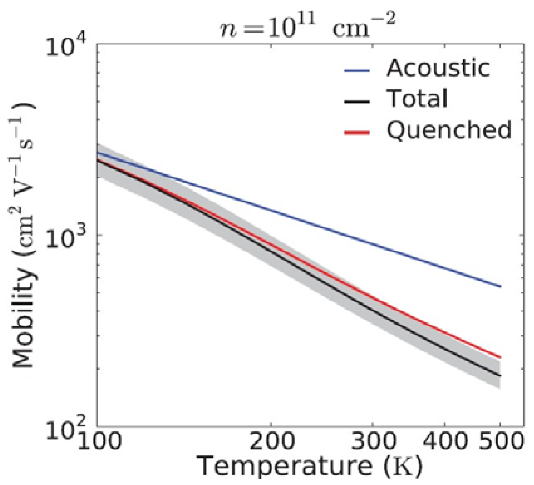
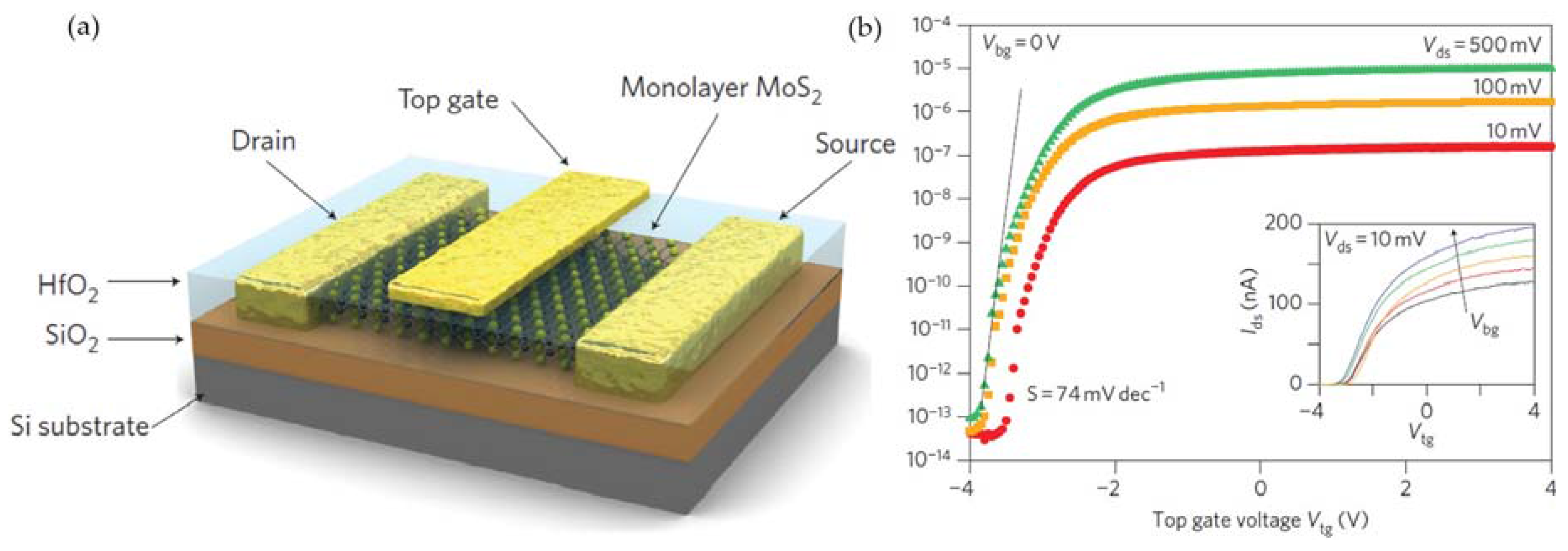
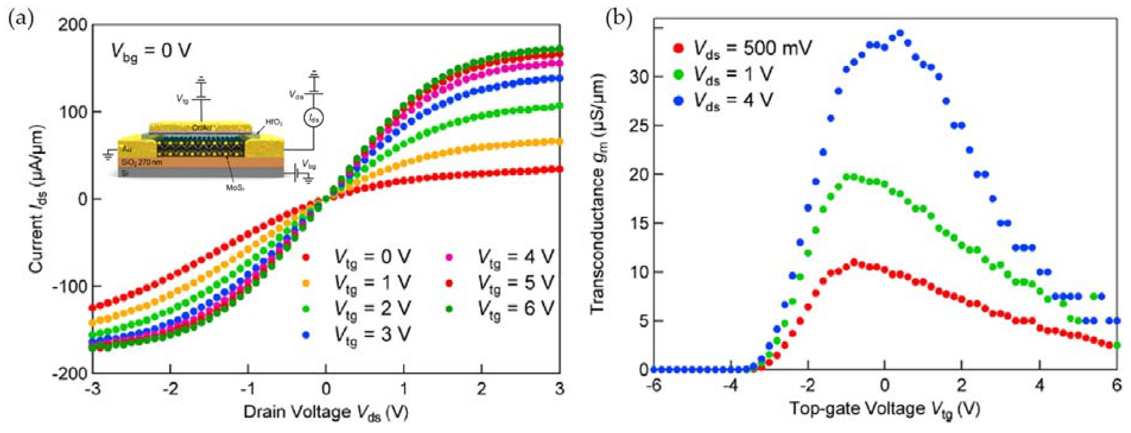
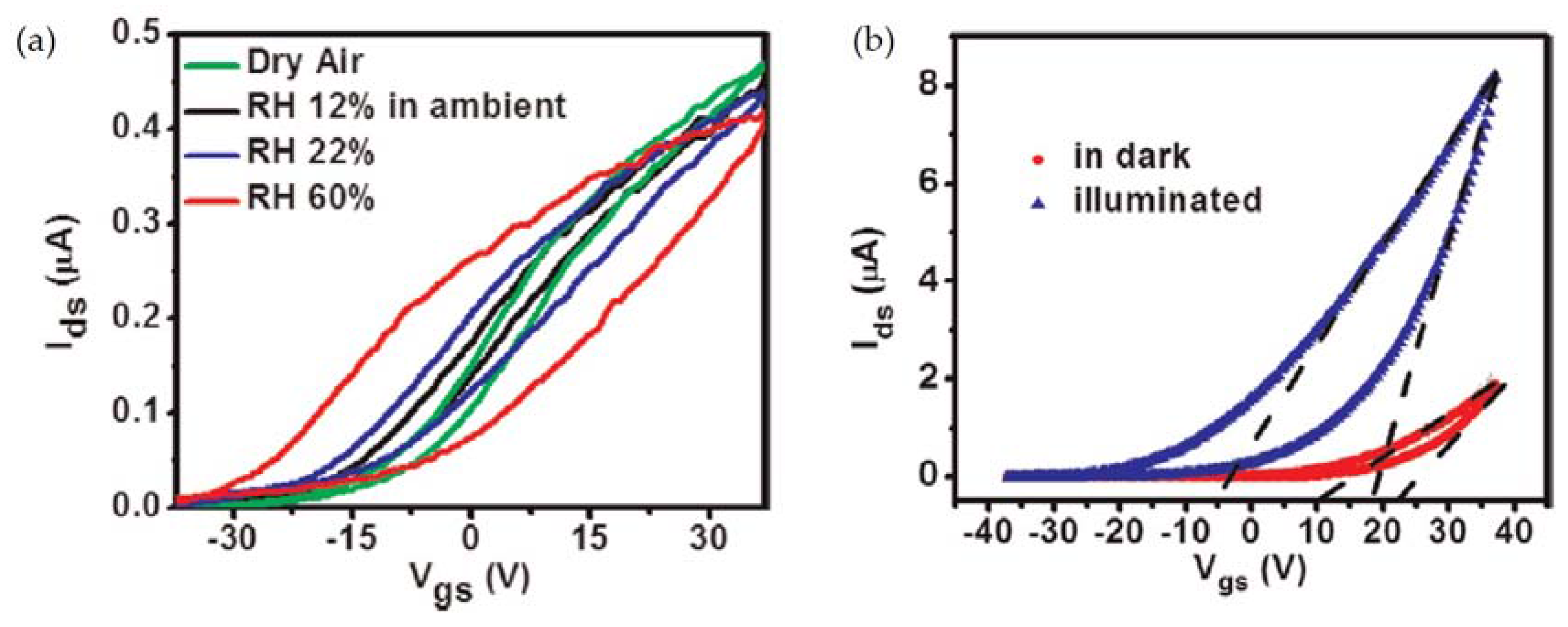
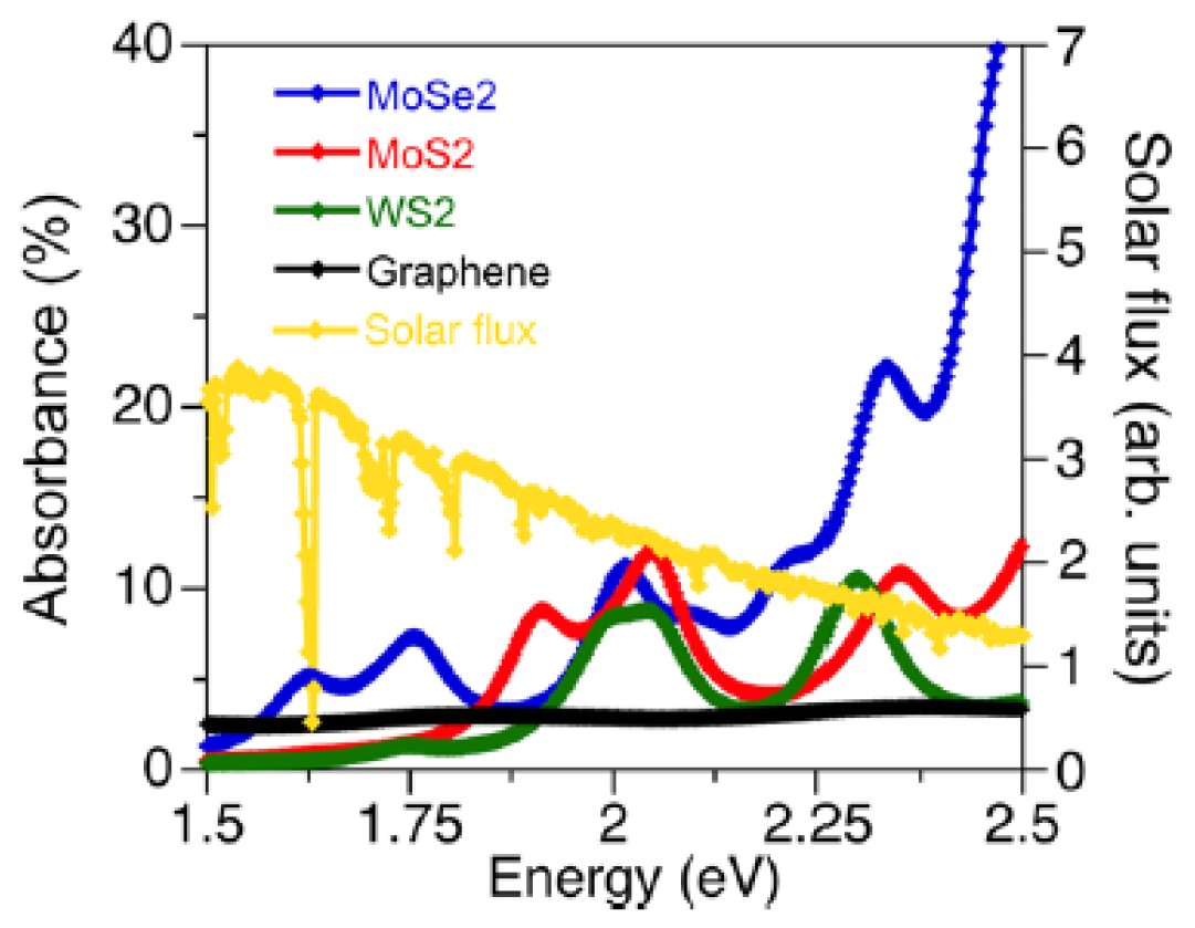
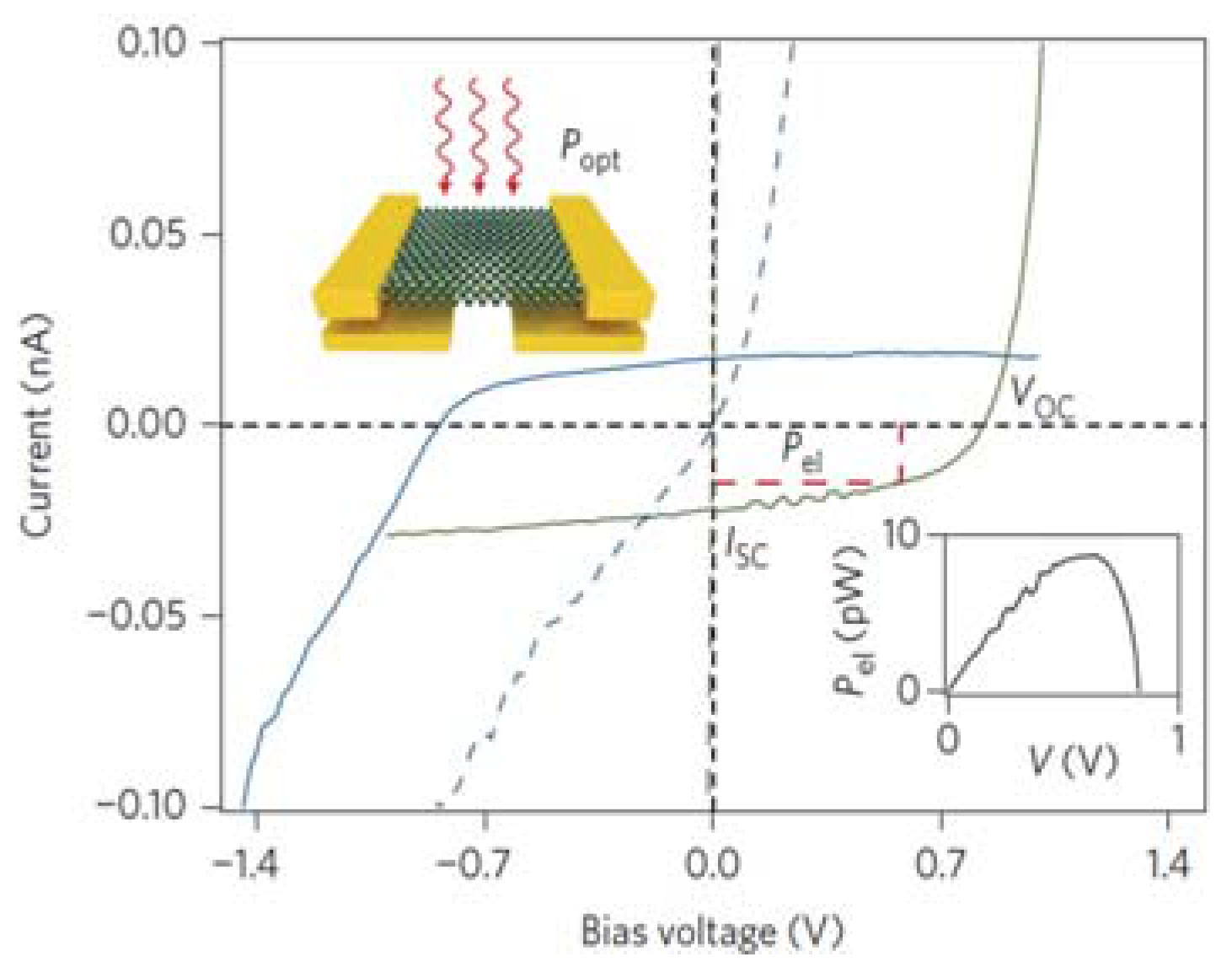
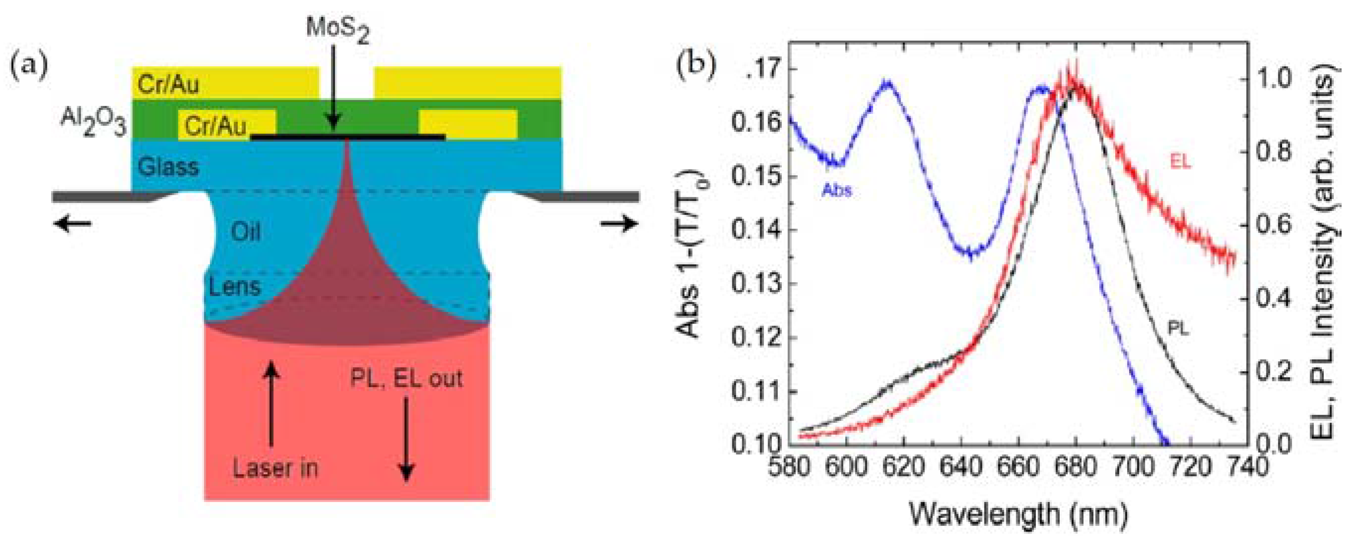
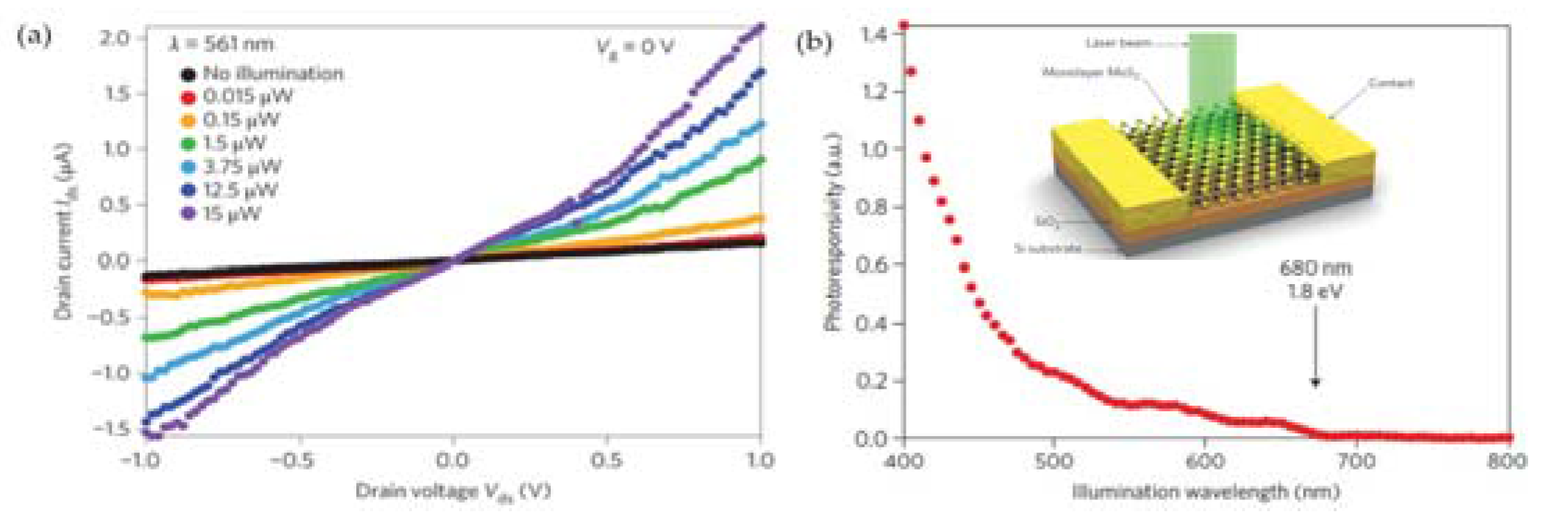
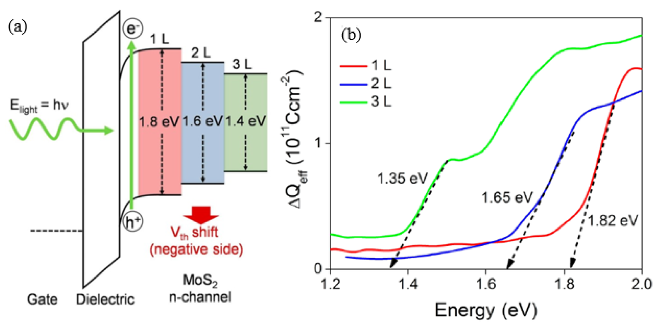
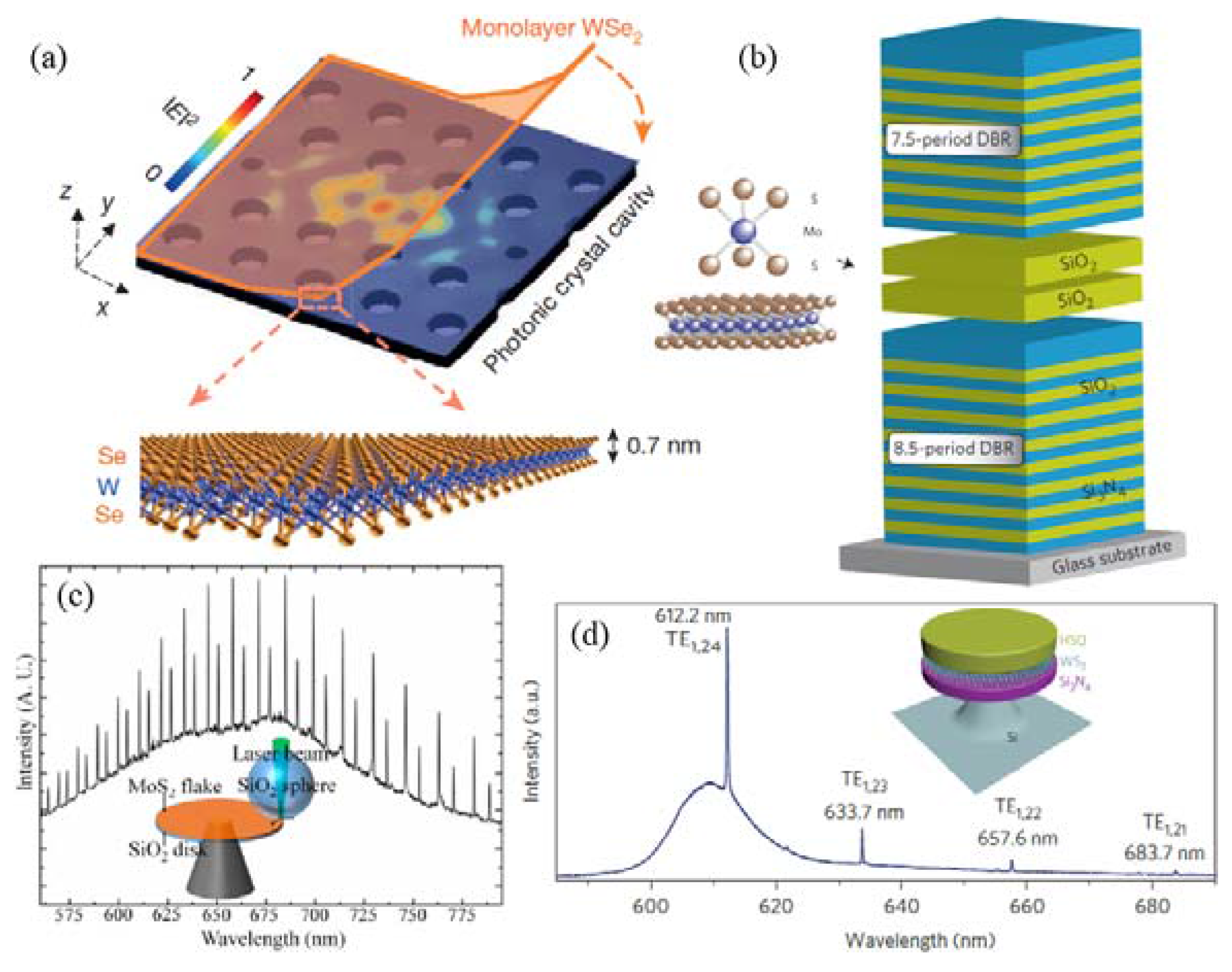
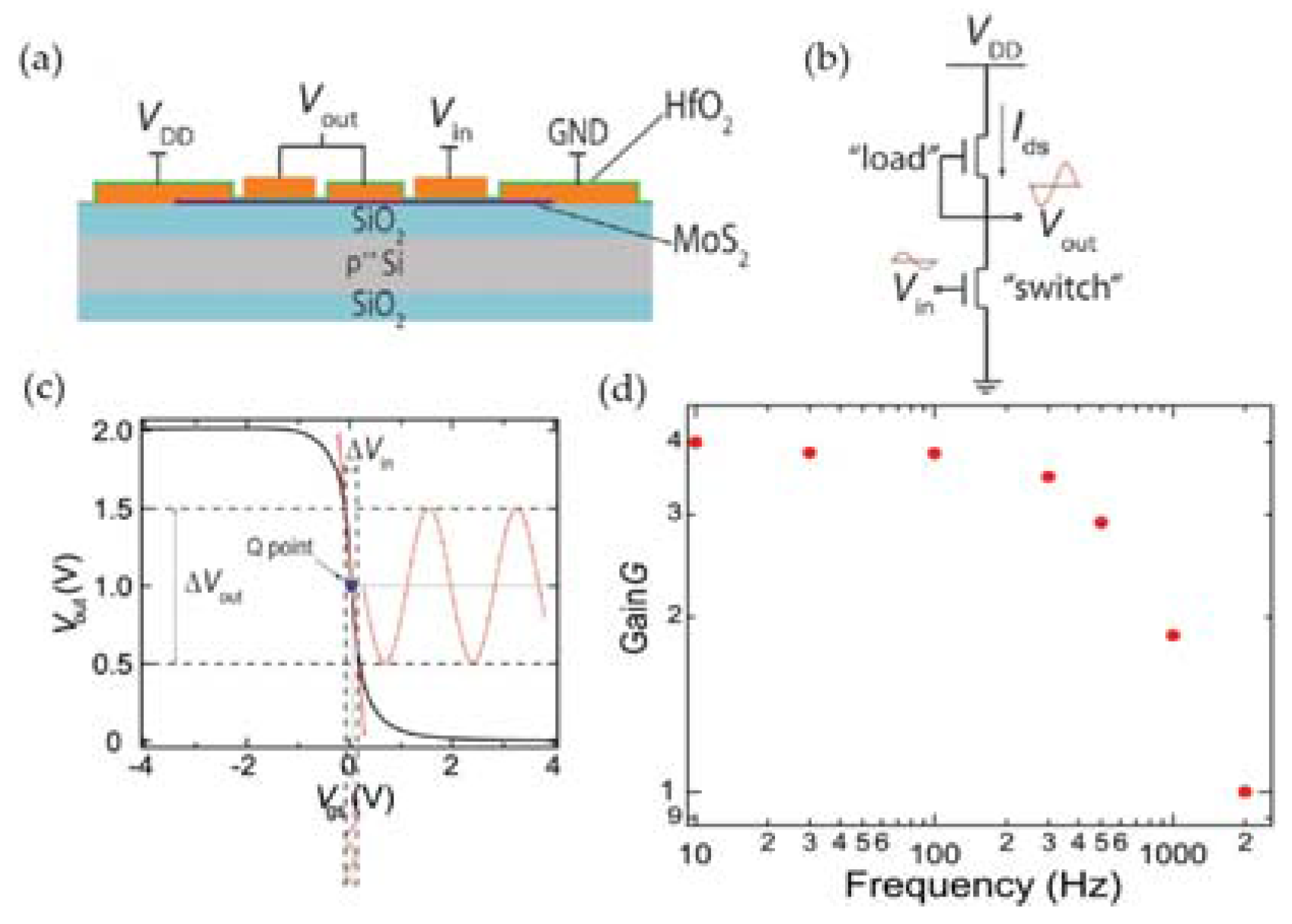
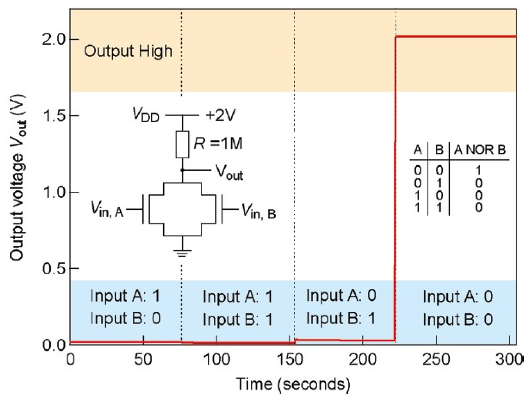
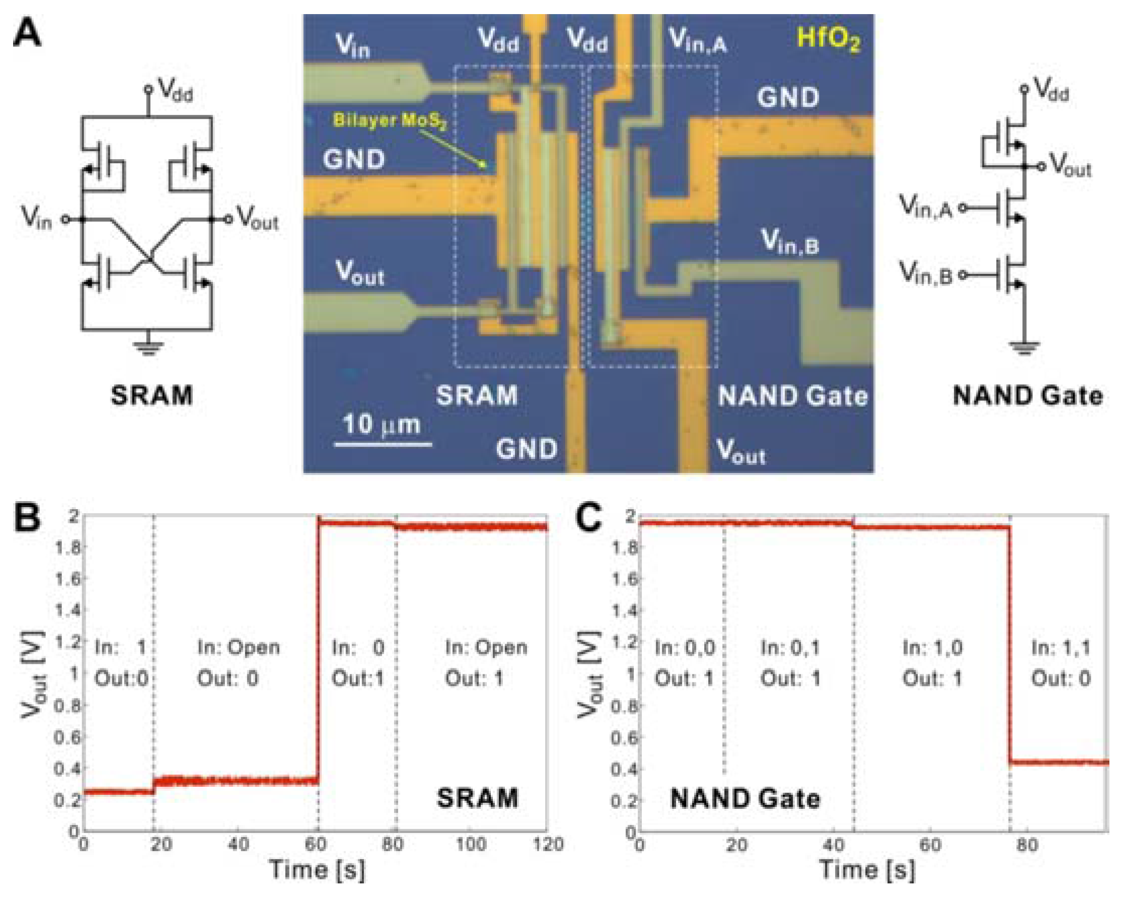
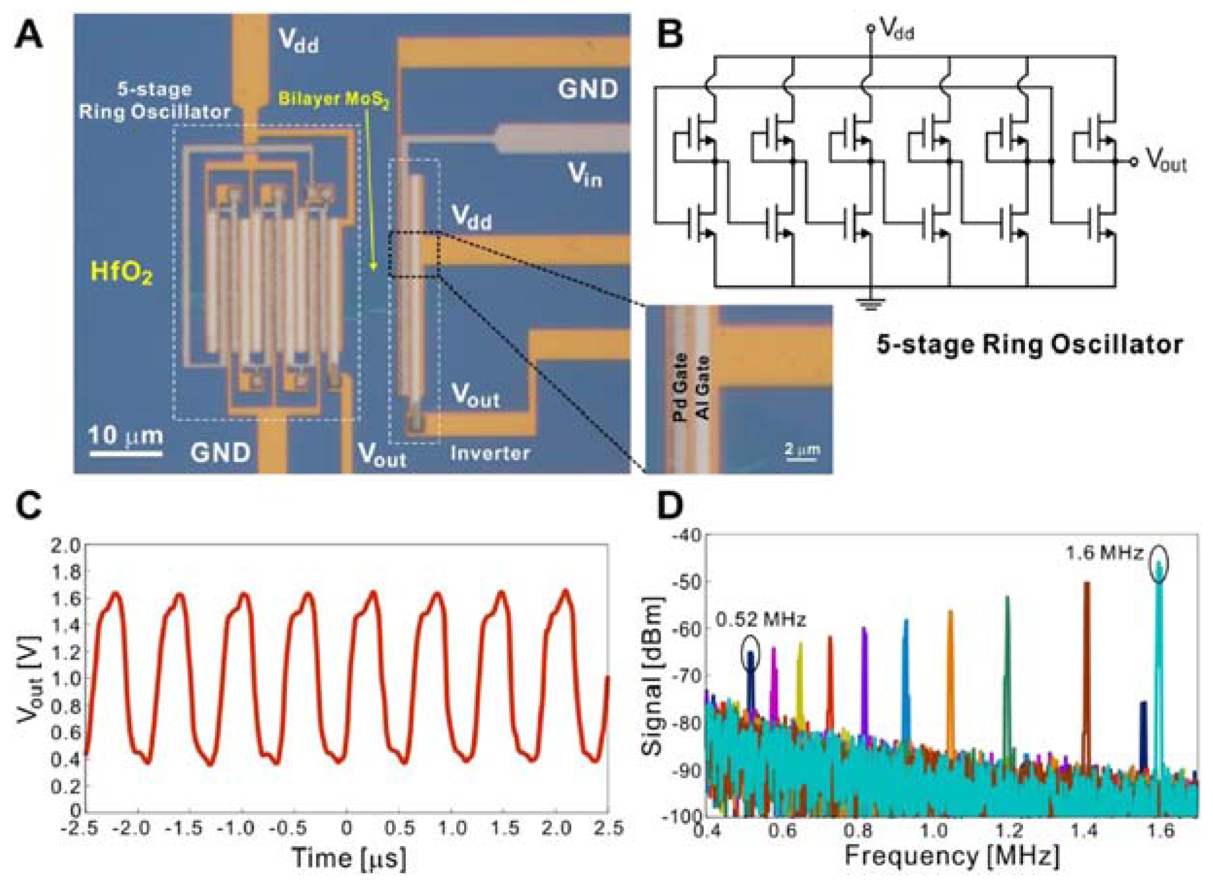
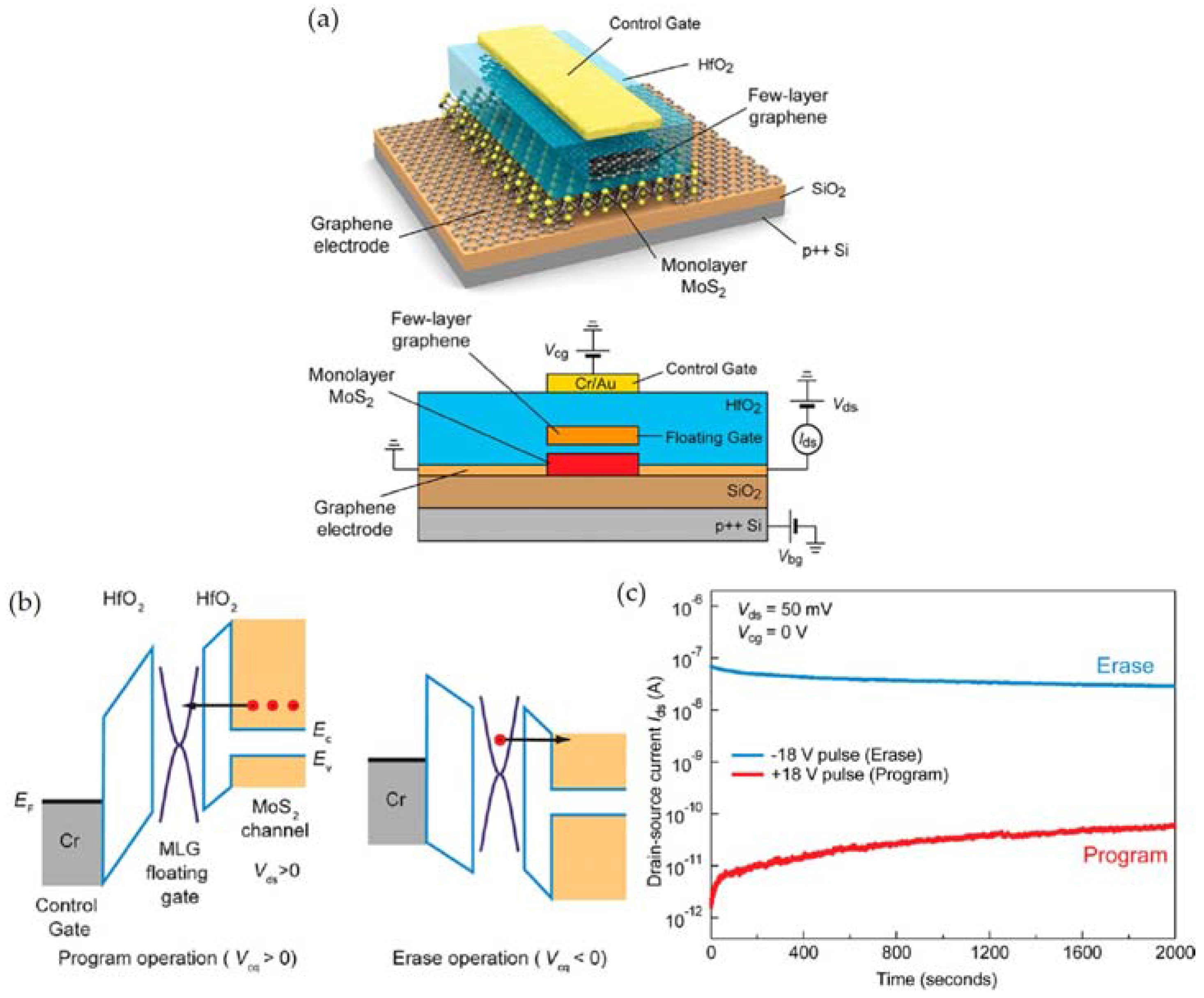


| M or X | S | Se | Te |
|---|---|---|---|
| Mo | 1L: ~1.8–1.9 eV (D) Bulk: 1.2 eV (I) [10] | 1L: 1.34 eV (D)(T) [11] 1L: 1.58 eV (D)(E) [12] Bulk: 1.1 eV (I)(E) [13] Bulk: 1.1 eV (I)(T) [14] | 1L: 1.07 eV (D)(T) [15] 1L: 1.1 eV (D)(E) [16] Bulk: 1.0 eV (I)(E) [17] 0.82 eV (I)(T) [18] |
| W | 1L: 1.94 eV (D)(T) [19] 1L: 2.14 eV (D)(E) [20] Bulk: 1.35 eV (I)(E) [21] | 1L: 1.74 eV (D)(T) [19] 1L: 1.65 eV (D)(E) [22] Bulk: 1.1 eV (I)(D) [23] Bulk: 1.2 eV (I)(E) [21] | 1L: 1.14 eV (D)(T) [19] Bulk: 0.7 eV (I)(T) [23] |
| Re | 1L: 1.43 eV (D)(T) [24] 1L: 1.55 eV (D)(E) [24] Bulk: 1.35 eV (D)(T) [24] Bulk: 1.47 eV (D)(E) [25] | 1L: 1.34 eV (I)(T) [26] 1L: 1.239 eV (D)(T) [27] 1L: 1.47 eV (I)(E) [28] 2L: 1.165 eV (D)(T) [27] 2L: 1.32 eV (I)(E) [29] 4L: 1.092 eV (D)(T) [27] Bulk: 1.06 eV (I)(T) [26] Bulk: 1.18 (I)(E) [30] |
| Materials | Configuration (Method) | Mobility (cm2·V−1·s−1) | On/Off Ratio | Subthreshold Swing (mV·dec−1) | Temperature (K) | Reference |
|---|---|---|---|---|---|---|
| MoS2 | Back-gated | 3 | 300 | [41] | ||
| Back-gated | 40 | 105 | 1000 | 300 | [42] | |
| Back-gated (CVD) | 2 × 10⁻² | 104 | 300 | [45] | ||
| Back-gated | 100 | 106 | 80 | 300 | [46] | |
| Back-gated | 2.4 | 107 | 300 | [47] | ||
| Dual-gated | 517 | 108 | 140 | 300 | [48] | |
| Back-gated | 700 | 300 | [49] | |||
| Back-gated (CVD) | 17 | 4 × 10⁸(bi-) 104(multi-) | 300 | [50] | ||
| Four-terminal Back-gated | 306.5 | 106 | 300 | [51] | ||
| Four-terminal Top-gated | 470(e)/480(h) | 300 | [52] | |||
| ZrO2 & CNT Back-gated | 106 | 3 | [53] | |||
| MoSe2 | Back-gated | 50 | 106 | 300 | [54] | |
| Four-terminal Back-gated on SiO2/parylene-C (CVD) | 50(Si) 160(parylene-C) 500 | 106(e) 103(h) | 295/100 | [55] | ||
| Four-terminal Back-gated (CVD) | 200(e)/150(h) | 106 | 275 | [56] | ||
| Back-gated (CVD) | 10 | 103 | 300 | [57] | ||
| MoTe2 | Back-gated | 0.03(e)/0.3(h) | 2 × 10³ | 300 | [58] | |
| Four-terminal Back-gated | 20(h) | 105 | 140 | 300 | [59] | |
| Ionic Liquid Top-gated | 30(e)/10(h) | 140(e)/125(h) | 300 | [60] | ||
| Back-gated | 6(h) | 105 | 300 | [61] | ||
| Solid Polymer Electrolyte Back-gated | 7(e)/26(h) | 105 | 90 | 300 | [62] | |
| Back-gated | 25.2(e)/1.5(h) | 2.1 × 10⁵(e)/5.7 × 104(h) | 280 | [63] | ||
| Back-gated | 2.04(h) | 300 | [64] | |||
| WS2 | Iodine-transport Back-gated (PVD) | 105 | 300 | [65] | ||
| Ionic Liquid Top-gated | 20(e)/90(h) | 90 | 300 | [66] | ||
| Ionic Liquid Top-gated | 19(e)/12(h) | 106 | 63(e)/67(h) | 300 | [20] | |
| Back-gated | 234 | 108 | 300 | [67] | ||
| Four-terminal Back-gated | 20 | 106 | 70 | 300 | [68] | |
| WSe2 | Four-terminal Top-gated | 500(h) | 300 | [40] | ||
| Ionic Liquid Top-gated | 200(e/h) 330(e)/270(h) | 10 | 170/160/77 | [69] | ||
| Back-gated (CVD) | 350(h) | 108 | 300 | [70] | ||
| Back-gated (CVD) | 650(h) | 106 | 250/140 | 150/300/105 | [71] | |
| Back-gated (CVD) | 10(h) | 104 | 300 | [72] | ||
| Back-gated | 92(h) | ~10 | 300 | [73] | ||
| ReS2 | Dual-gated | 12/26 | 105 | 148 | 300/77 | [74] |
| Dual-gated | 1/5 | 106 | 750 | 300/120 | [75] | |
| Back-gated | 15.4 | 107 | 100 | 300 | [76] | |
| Back-gated | 1.5 | 105 | 300 | [77] | ||
| Back-gated | 11 | 3 × 10⁵ | 300 | [78] | ||
| Back-gated (CVD) | 7.2 × 10⁻² | 103 | 300 | [79] | ||
| ReSe2 | Top-gated | 0.1 | 300 | [27] | ||
| Back-gated | 6.7 | 105 | 1300 | 300 | [80] | |
| Back-gated (CVD) | 1.36 × 10⁻³(h) | 300 | [81] |
| Materials | Configuration (Method) | Mobility (cm2·V−1·s−1) | On/Off Ratio | Subthreshold Swing (mV·dec−1) | Temperature (K) | Reference |
|---|---|---|---|---|---|---|
| MoS2 | Top-gated | 217 | 108 | 74 | 300 | [82] |
| Simulation Top-gated | 350 | 1010 | 60 | 300 | [96] | |
| Back-gated | 12 | 300 | [83] | |||
| Top-gated | 320 | 106 | 300 | [97] | ||
| Back-gated (CVD) | 0.04 | 300 | [98] | |||
| Back-gated | 10 | 106 | 300 | [99] | ||
| Polymer Electrolyte Top-gated | 10 | 106 | 60 | 300 | [100] | |
| Ferro-electric polymer Top-gated | 220 | 105 | 300 | 300 | [101] | |
| Top-gated | 380 | 106 | 500 | 300 | [102] | |
| Top-gated | 1090 | 108 | 178 | 300 | [103] | |
| Back-gated (CVD) | 8 | 107 | 300 | [84] | ||
| Multi-terminal Back-gated | 1000 | 106 | 4 | [104] | ||
| Back-gated (CVD) | 6 | 105 | 300 | [105] | ||
| Top-gated On SiO2/Si3N4 (CVD) | 55(Si3N4) 24(SiO2) | 107(SiO2) | 300 | [106] | ||
| Top-gated (CVD) | 42.3 | 106 | 300 | [107] | ||
| Dual-gated (CVD) | 190 | 108 | 170 | 300 | [108] | |
| MoSe2 | Back-gated (CVD) | 0.02(e)/0.01(h) | 102 | 300 | [109] | |
| Back-gated (CVD) | 50 | 106 | 300 | [110] | ||
| Back-gated (CVD) | 23(e)/17(h) | 105 | 300 | [111] | ||
| WS2 | Ionic Liquid Top-gated | 44(e)/43(h) | 105 | 52(e)/57(h) | 300 | [20] |
| Back-gated | 50/140 | 106 | 300/83 | [112] | ||
| Back-gated (CVD) | 4.1 | 105 | 300 | [113] | ||
| Back-gated | 83/337 | 300/25 | [114] | |||
| WSe2 | Top-gated | 250(h) | 106 | 60 | 300 | [115] |
| Ionic Liquid Top-gated | 90(e)/7(h) | 104(e) 105(h) | 300 | [116] | ||
| Polymer electrolyte Back-gated | 30(e)/180(h) | 300 | [117] | |||
| Back-gated (CVD) | 100(h) | 108 | 300 | [70] |
| Materials and Structure | On/Off Ratio | On-Current Density (A/cm2) | Off-Current Density (A/cm2) | Source–Drain Voltage (V) | Reference |
|---|---|---|---|---|---|
| Gr/MoS2/Ti | 60 (290 K) 104 (150 K) | 60 | 0.5 | 0.1 | [165] |
| hBN/Gr/WS2/Gr/Au | 106 | 200 | 0.001 | 0.2 | [166] |
| Gr/MoS2/Ti/Au | 102 | 150 | <1 | 0.01 | [169] |
| Gr/MoS2/Ti/Au | 103 | 5000 | 12.5 | 7 | [170] |
| Gr/MoS2/Ti/Au | 105 | 5 × 10⁴ | 0.1 | 0.5 | [171] |
| Gr/MoS2/Ti/Au | 3 | 50 | 1.5 | 0.05 | [172] |
| Gr/MoSe2/Ti/Au | 105 | 1000 | 0.05 | 0.5 | [167] |
| Au/Gr/MoS2 | 106 | 1000 | 0.0014 | 0.5 | [173] |
| Gr/WSe2/Provskite/Gr | 106 | <1 | <10−5 | −1 | [174] |
| Gr/MoS2/Au | 104 | 3000 | 0.3 | 0.5 | [168] |
| Gr/WSe2/Au | 104 | 3100 | 0.31 | 0.5 | |
| APTES/Gr/WSe2/Pt | 3 × 10⁴ (300 K) 5 × 10⁷ (180 K) | 11 | 0.001 | 0.1 | [175] |
| Materials and Structure | Type | EL Peak (nm) | EL Efficiency | Reference |
|---|---|---|---|---|
| Au/Cr/MoS2/Cr/Au | Schottky junction | 685 | 0.001% | [202] |
| Ti/WSe2/Ti | p–i–n junction | 740 | 0.06% | [203] |
| Au/Pd/WSe2/Ti/Au | p–n junction | 800 | 0.1% | [157] |
| Au/WSe2/Pt | p–n junction | 752 | 0.2% | [158] |
| Au/WSe2/Au | p–n junction | 750 | 0.1% | [159] |
| Ni/MoS2/WSe2/Au | p–n junction | 800 | 12% | [184] |
| Gr/hBN/MoS2/hBN/Gr | Tunnel junction | 678 | 8.4% | [204] |
| Gr/hBN/WS2/hBN/Gr | 620 | 1.32% | ||
| Gr/hBN/WSe2/hBN/Gr | 738 | 5.4% |
| Materials | P/E Ratio | Endurance (Cycles) | Retention (s) | Operating Voltage(V) | Reference |
|---|---|---|---|---|---|
| MoS2 (with PZT) | 5 × 10³ | 103 | 1 | [101] | |
| 104 | 500 | 104 | 0.1 | [250] | |
| 104 | 120 | 2 × 10³ | 0.05 | [251] | |
| Graphene/MoS2 | 104 | 120 | 2 × 10³ | 0.05 | [252] |
| Graphene/hBN/MoS2 | 105 | 120 | 1.4 × 10³ | 0.05 | [253] |
| 105 | 105 | 104 | 8 | [254] | |
| MoS2/hBN/BP | 50 | 40 | 103 | 0.05 | [113] |
© 2017 by the authors. Licensee MDPI, Basel, Switzerland. This article is an open access article distributed under the terms and conditions of the Creative Commons Attribution (CC BY) license (http://creativecommons.org/licenses/by/4.0/).
Share and Cite
Ye, M.; Zhang, D.; Yap, Y.K. Recent Advances in Electronic and Optoelectronic Devices Based on Two-Dimensional Transition Metal Dichalcogenides. Electronics 2017, 6, 43. https://doi.org/10.3390/electronics6020043
Ye M, Zhang D, Yap YK. Recent Advances in Electronic and Optoelectronic Devices Based on Two-Dimensional Transition Metal Dichalcogenides. Electronics. 2017; 6(2):43. https://doi.org/10.3390/electronics6020043
Chicago/Turabian StyleYe, Mingxiao, Dongyan Zhang, and Yoke Khin Yap. 2017. "Recent Advances in Electronic and Optoelectronic Devices Based on Two-Dimensional Transition Metal Dichalcogenides" Electronics 6, no. 2: 43. https://doi.org/10.3390/electronics6020043
APA StyleYe, M., Zhang, D., & Yap, Y. K. (2017). Recent Advances in Electronic and Optoelectronic Devices Based on Two-Dimensional Transition Metal Dichalcogenides. Electronics, 6(2), 43. https://doi.org/10.3390/electronics6020043