Effects of Gate-Length Scaling on Microwave MOSFET Performance


1
Department of Biomedical and Dental Sciences and Morphofunctional Imaging, University of Messina, 98125 Messina, Italy
2
Electronic Engineering Department, KU Leuven, B-3001 Leuven, Belgium
3
Department of Engineering, University of Messina, 98166 Messina, Italy
*
Author to whom correspondence should be addressed.
Electronics 2017, 6(3), 62; https://doi.org/10.3390/electronics6030062
Submission received: 5 August 2017
/
Revised: 22 August 2017
/
Accepted: 25 August 2017
/
Published: 30 August 2017
Abstract
:This paper focuses on the extraction of an accurate small-signal equivalent circuit for metal-oxide-semiconductor field-effect transistors (MOSFETs). An analytical modeling approach was developed and successfully validated through the comparison between measured and simulated scattering parameters. The extraction of the equivalent circuit elements allowed for the estimation of the intrinsic unity current-gain cutoff frequency, which is a crucial figure of merit for assessing the high-frequency performance. The experimental data show that the cutoff frequency of the tested devices exhibits a nearly ideal scaling behavior with decreasing gate length.
1. Introduction
The extraction of an accurate small-signal equivalent circuit is of great importance for evaluating microwave field-effect transistor (FET) performance. This is because the equivalent circuit provides a physically meaningful description of the physical device structure. Furthermore, the extraction of the circuit elements allows for the estimation of relevant figures of merit, such as the intrinsic unity current-gain cutoff frequency (fT). The determination of this figure of merit is essential to assess the potential of the device for high-frequency operation. Driven by the ever-growing demand for high-frequency applications, continuous efforts are being made to develop innovative materials and architectures (e.g., high-mobility III-V and Ge channels, high-k dielectrics, and multiple-gates) [1,2,3,4,5]. The intrinsic fT is expected to remarkably increase with decreasing gate length and to be roughly independent of the gate width. Hence, a significant improvement of the high-frequency performance can be achieved with gate-length downscaling. Typically, the equivalent circuit is extracted from scattering (S-) parameters, which can be straightforwardly and accurately measured with a vector network analyzer. To accomplish this goal, several numerical optimization [6,7,8,9] and analytical [10,11,12,13,14,15,16] procedures have been proposed in the last four decades. The numerical optimization approach can yield non-physical values of the circuit elements, by which the results can critically depend on the initial element values, local minima, and the optimization technique itself. These drawbacks can be overcome by adopting the analytical approach that is based on first extracting the extrinsic bias-independent elements, then de-embedding their contributions with simple matrix manipulations, and finally calculating the intrinsic bias-dependent elements from the intrinsic admittance (Y-) parameters. The determination and subsequent de-embedding of the extrinsic elements is essential to access the performance of the intrinsic FET that is not directly measurable, since the intrinsic section of the FET is experimentally inaccessible. The extrinsic elements are usually determined using “cold” S-parameter measurements (VDS = 0 V, i.e., passive device) [10,11,12,13,14,15,16], passive test structures [13,14,15,16,17], and full-wave electromagnetic simulations [18,19,20,21]. In practice, the “cold” approach is the most used, since it does not require additional dummy structures or detailed information about the FET layout.
The present study aims to develop an analytical modeling technique to determine a small-signal equivalent circuit for three metal-oxide-semiconductor field-effect transistors (MOSFETs) with different gate lengths. In particular, the extrinsic capacitances are obtained from S-parameters measured on an open structure, whereas the extrinsic resistances and inductances are determined from “cold” S-parameter measurements. The open structure is used to extract the extrinsic capacitances, since the standard “cold” approach does not allow distinguishing clearly between extrinsic and intrinsic output capacitances [10,22]. The de-embedding of the extrinsic elements enables the calculation of the intrinsic elements, thereby allowing the estimation of fT and the analysis of the impact of the gate-length scaling on this figure of merit. It is noteworthy that a lossy substrate resistance is included in the intrinsic model in order to obtain good agreement between the measured and simulated output reflection coefficient.
The remainder of this paper is structured as follows: the next section contains a description of the tested devices and of the proposed modeling technique, the subsequent section discusses the experimental results, and the last section summaries the main conclusions of this study.
2. Model Extraction
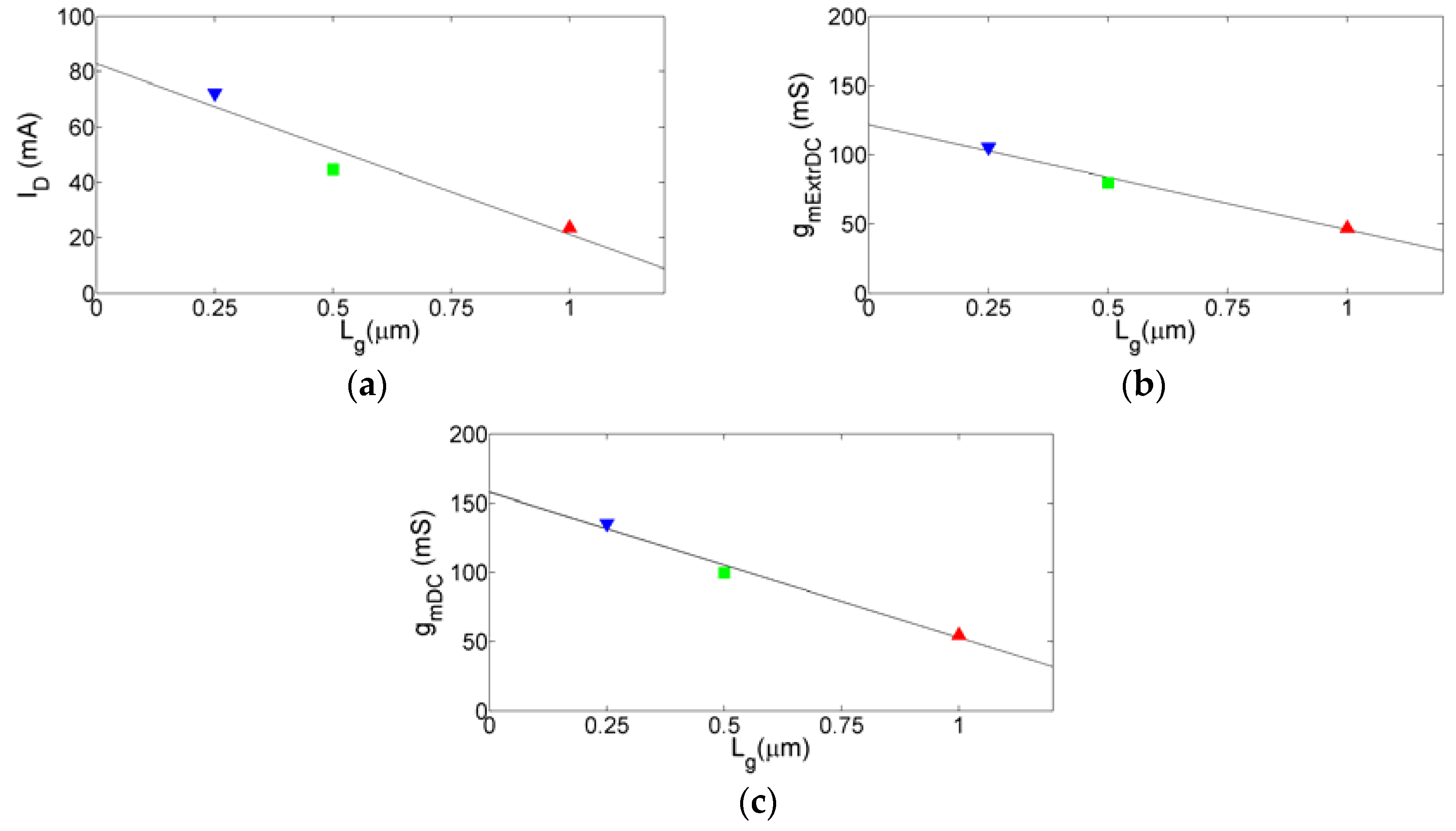
The tested devices are three multi-cell, multi-finger MOSFETs with a gate width of 192 μm (W = 16 × 4 × 3, 8 × 4 × 6, and 8 × 4 × 6 μm) and different gate lengths (Lg = 0.25, 0.5, and 1 μm). The measured DC output characteristics are reported in Figure 1. As can be observed, a quite good scaling of the drain current is achieved. This is highlighted in Figure 2, showing that the drain current and transconductance increase roughly linearly with inverse gate length. Although the extrinsic contributions imply a reduction of the transconductance, both extrinsic and intrinsic transconductances (gmExtrDC and gmDC) exhibit good scaling. It should be underlined that the scaling of DC and RF properties are strongly correlated with each other, since RF performance strongly depends on the associated DC bias point.
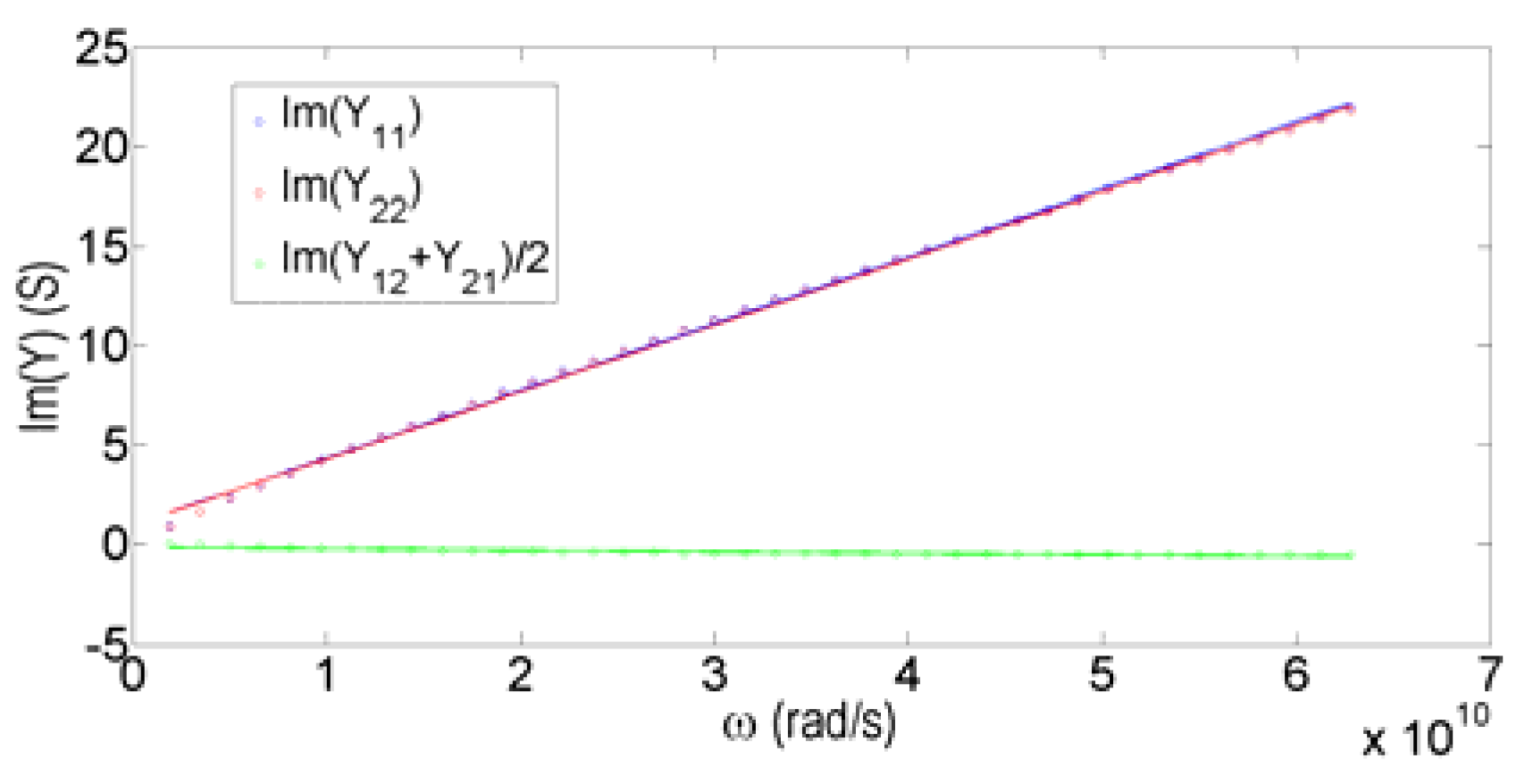
Figure 3 illustrates the small-signal equivalent circuit that is used to reproduce the measured S-parameters of the tested MOSFETs. This circuit can be divided into two main sections: the extrinsic and intrinsic parts. The extrinsic section is composed by eight bias-independent elements (Cpg, Cpd, Lg, Ls, Ld, Rg, Rs, and Rd), while the intrinsic section consists of eight bias-dependent elements (Cgs, Cgd, Cds, Rgs, Rds, Rsub, gm, and τ). In order to take into account the distributed effects, the extrinsic capacitances are split into two equal parts, placed outermost and innermost of the three extrinsic inductances. The extrinsic capacitances Cpg and Cpd are straightforwardly extracted from the imaginary parts of the Y-parameters of an open structure that has been fabricated on the same die of the same wafer of the tested MOSFETs. In general, the open structure can be represented with a pi network composed of three capacitances modeling the capacitive coupling between the pads. In most cases, as in the present one, the feedback capacitance can be disregarded, thereby allowing the determination of the input and output capacitances from the imaginary parts of Y11 and Y22, respectively. As illustrated in Figure 4, the extrinsic capacitances are extracted by using the frequency range from 0.3 to 10 GHz. After removing the effects of Cpg and Cpd, the extrinsic resistances and inductances are, respectively, obtained from the real and imaginary parts of Z-parameters with VDS = 0 V and VGS >> VTH by using the frequency range from 10 to 40 GHz. Under this bias condition, the intrinsic section of the MOSFET can be modeled through a distributed channel resistance and a distributed gate capacitance, leading to the following expressions of the Z-parameters [13]:
where Cg and Rch are the gate capacitance and the channel resistance, respectively.
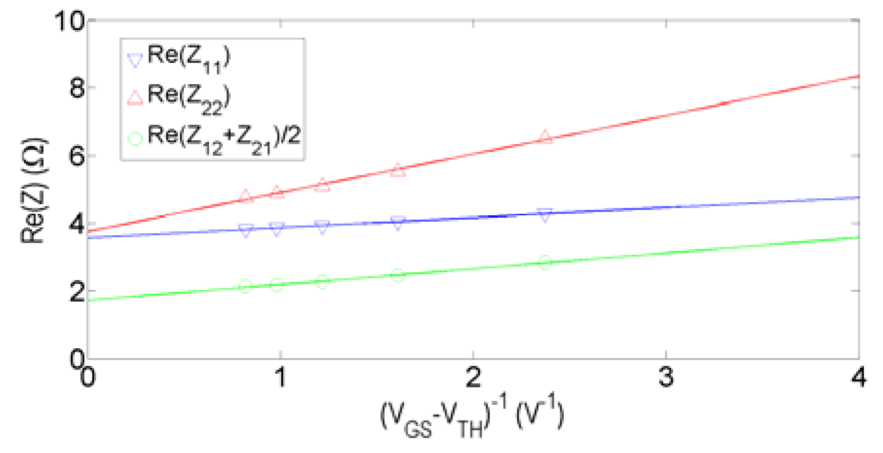
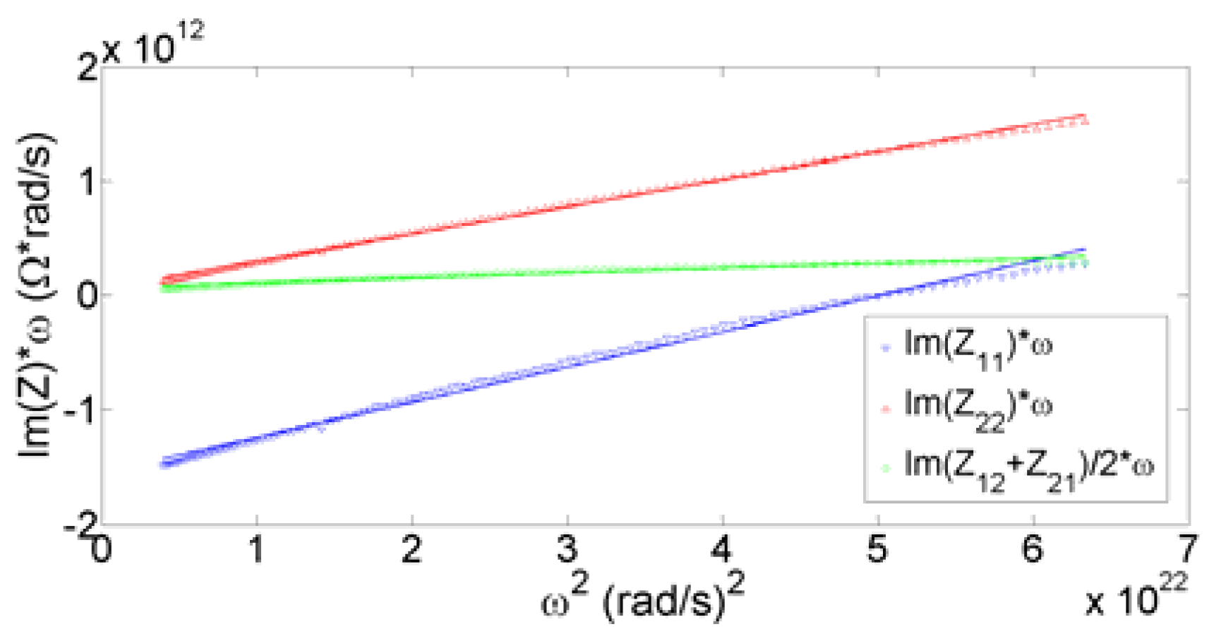
By assuming Rch to be proportional to 1/(VGS − VTH) at “cold” condition [13], the extrinsic resistances can be straightforwardly determined from the intercept coefficients of the three linear regressions of Re(Zij) versus 1/(VGS − VTH) (see Figure 5). In order to minimize the frequency dependence of Re(Zij) associated with an incomplete capacitance de-embedding and/or intrinsic capacitive effects, Re(Zij) is obtained at each gate voltage from the slope of the straight line approximating ω2Re(Zij) versus ω2. The extrinsic inductances are extracted from the slopes of the straight lines approximating ωIm(Zij) versus ω2 (see Figure 6).
After de-embedding all of the parasitic effects’ elements by means of simple matrix operations, the intrinsic elements can be obtained from the intrinsic Y-parameters at each bias condition. It is worth noting that, analogously to what has been done for fin field-effect transistors (FinFETs) [14], Rds, Cds, and Rsub are determined from the real and imaginary part of the intrinsic Y22 + Y12. In particular, Rds is calculated at low frequencies by treating the RsubCds series network as an open circuit, and then its contribution is removed to enable the extraction of Cds and Rsub:
The introduction of Rsub does not affect the calculation of the intrinsic fT, which is determined with the output short-circuited. The intrinsic unity current-gain cutoff frequency can be straightforwardly estimated from the intrinsic elements of the equivalent circuit as follows:
This equation shows that fT is directly proportional to gm and inversely proportional to the total gate capacitance Cgg, given by the sum of Cgs and Cgd. The capacitance Cgg should be directly proportional to both gate width and gate length, while the conductance gm should be directly proportional to the gate width and inversely proportional to the gate length. As a result, fT is expected to be inversely proportional to the square of the gate length and to be roughly independent of the gate width. However, deviations from this ideal behavior can be observed, due to non-ideal effects such as thermal phenomena and short channel effects. For example, fT can be found to inversely scale with the gate length, due to saturation velocity in short channel devices. In such a case, the cutoff frequency can be used to estimate the saturation velocity as 2πLgfT. Furthermore, under- and/or over-de-embedding of the extrinsic contributions may critically affect the results of the scaling analysis for the intrinsic section.
3. Model Validation and Discussion
The validity of the proposed technique is confirmed by the good agreement between the measured and simulated S-parameters. As an illustrative example, Figure 7 shows the comparison between the measured and simulated S-parameters from 0.3 to 40 GHz for the three tested devices at VGS = 1 V and VDS = 1 V. It should be highlighted that, by decreasing the gate length, the magnitude of the low-frequency forward transmission coefficient S21 increases, due to the improvement of the transconductance, and the starting point of output reflection coefficient S22 moves farther from the open circuit condition, due to the reduction of the drain-source resistance. This result can be easily explained by considering that, as the frequency tends to zero, the transconductance delay can be neglected and all inductors and capacitors can be, respectively, replaced with short and open circuits, and thereby S21 and S22 can be defined as follows [23]:
where R0 is the characteristic resistance (i.e., 50 Ω), while gmExtr and RdsExtr represent the extrinsic transconductance and drain-source resistance:
To illustrate the necessity of including Rsub in the model, Figure 8 shows that the measured S22 is not accurately reproduced by disregarding Rsub. As a matter of fact, Rsub is required to add a resistive contribution in order to enhance the accuracy of the simulated S22.
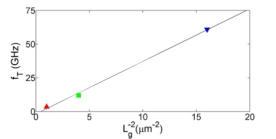
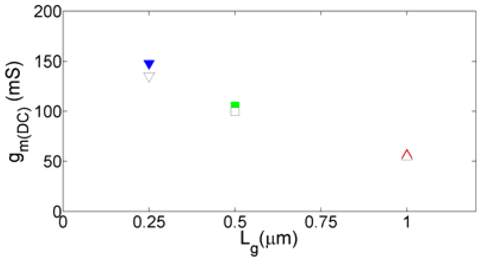
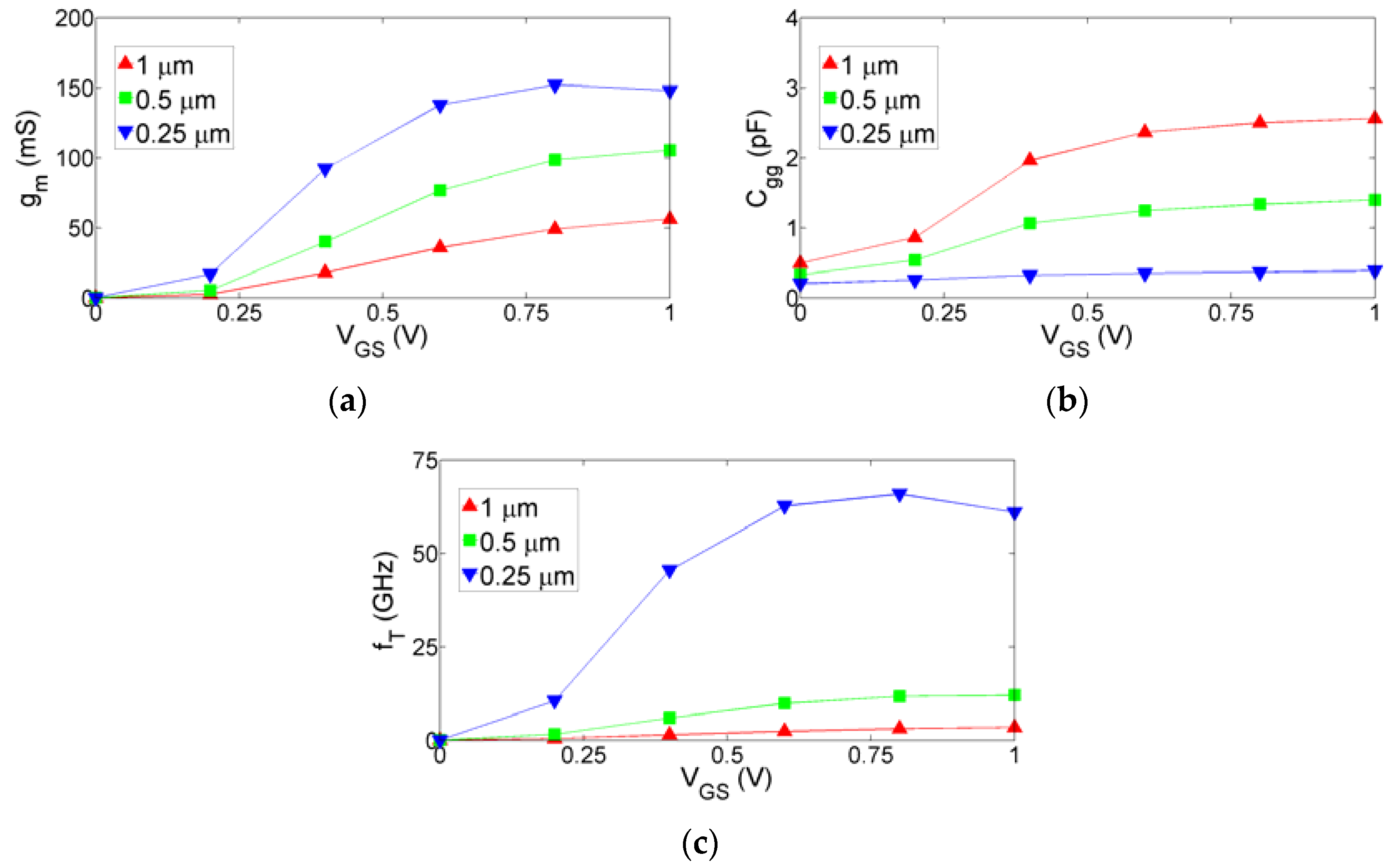
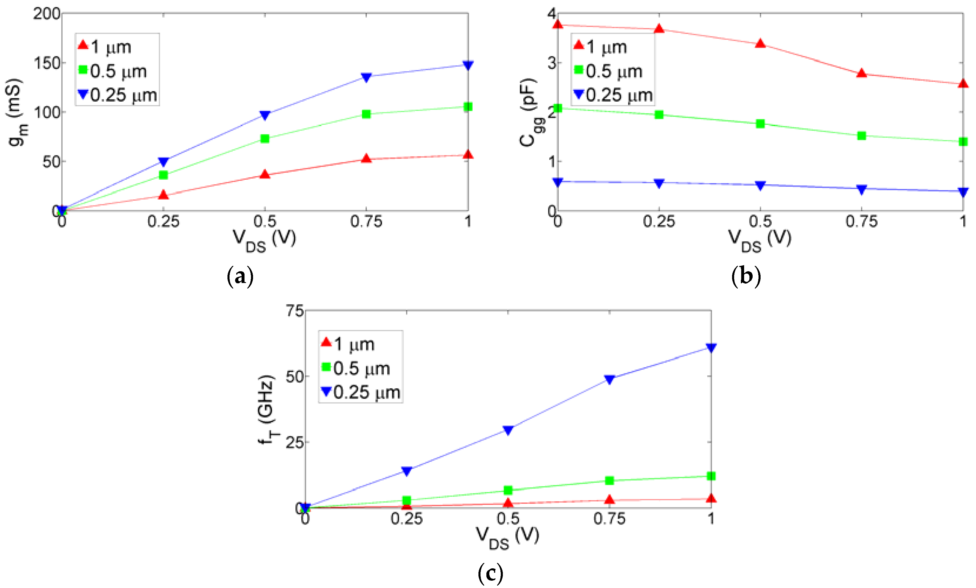
By focusing the analysis on the scaling of fT, Figure 9 shows that a significant improvement of fT is achieved with decreasing gate length. In particular, fT scales inversely with the square of the gate length, as in the ideal case. In agreement with the expectation, this result is due to the achieved good scaling of gm and Cgg with the gate length. Although Cgg is usually mostly determined by Cgs, Cgd has been considered to estimate fT, since its contribution becomes relevant by decreasing VDS and/or VGS. Furthermore, it is noteworthy that, although some slight discrepancy is observed with decreasing gate length, the achieved values of gm are very close to those of the intrinsic transconductance calculated from DC measurements, indicating that the low-frequency dispersion plays a negligible role (see Figure 10). For the sake of completeness, the scaling of fT, gm, and Cgg versus the gate length is analyzed under a wide range of bias conditions (see Figure 11 and Figure 12). By fixing the input or the output voltage, a good scaling of fT with decreasing gate length is always obtained, due to the increase of gm and the reduction of Cgg.
Finally, it should be pointed out that the achieved good scaling of the intrinsic performance of the tested devices implies that the extraction of the model for a few gate lengths allows for the prediction of the intrinsic performance, as well as for other lengths that fall into the studied range.
4. Conclusions
An analytical technique has been proposed to extract the small-signal equivalent circuits for MOSFFETs. The extrinsic elements have been determined using an open structure and “cold” FET measurements. The validity of the obtained models has been confirmed by the achieved good agreement between the measured and simulated S-parameters. The experimental data have shown that the presence of the substrate resistance in the intrinsic model is necessary to accurately reproduce the behavior of the measured output reflection coefficient. Furthermore, it has been found that the intrinsic unity current-gain cutoff frequency of the tested devices scales inversely with the square of the gate length, exhibiting a nearly ideal scaling.
Acknowledgments
The authors wish to acknowledge financial support by FWO and Hercules.
Author Contributions
Giovanni Crupi performed the experimental analysis and wrote the article. Dominique M. M.-P. Schreurs and Alina Caddemi supervised the research, provided technical feedback, and reviewed the article.
Conflicts of Interest
The authors declare no conflict of interest.
References
- Takagi, S.; Kim, S.-H.; Yokoyama, M.; Zhang, R.; Taoka, N.; Urabe, Y.; Yasuda, T.; Yamada, H.; Ichikawa, O.; Fukuhara, N.; et al. High mobility CMOS technologies using III-V/Ge channels on Si platform. Solid-State Electron. 2013, 88, 2–8. [Google Scholar] [CrossRef]
- Shi, M.; Saint-Martin, J.; Bournel, A.; Querlioz, D.; Wichmann, N.; Bollaert, S.; Danneville, F.; Dollfus, P. Monte Carlo analysis of the dynamic behavior of III-V MOSFETs for low-noise RF applications. Solid-State Electron. 2013, 87, 51–57. [Google Scholar] [CrossRef]
- Li, Z.; Niu, G.; Liang, Q.; Imura, K. Intermodulation linearity in high-k/metal gate 28 nm RF CMOS transistors. Electronics 2015, 4, 614–622. [Google Scholar] [CrossRef]
- Colinge, J.-P. Multiple-gate SOI MOSFETs. Microelectron. Eng. 2007, 84, 2071–2076. [Google Scholar] [CrossRef]
- Zota, C.B.; Lindelöw, F.; Wernersson, L.-E.; Lind, E. High-frequency InGaAs tri-gate MOSFETs with fmax of 400 GHz. Electron. Lett. 2016, 52, 1869–1871. [Google Scholar] [CrossRef]
- Li, S.; Cheng, J.; Han, B.; Gao, J. Bias-dependent small-signal modeling based on neuro-space mapping for MOSFET. Int. J. RF Microw. Comput.-Aided Eng. 2011, 12, 182–189. [Google Scholar] [CrossRef]
- Marinković, Z.; Markovic, V. Temperature-dependent models of low-noise microwave transistors based on neural networks. Int. J. RF Microw. Comput.-Aided Eng. 2005, 15, 567–577. [Google Scholar] [CrossRef]
- Marinković, Z.; Crupi, G.; Caddemi, A.; Marković, V. Comparison between analytical and neural approaches for multibias small signal modeling of microwave scaled FETs. Microw. Opt. Technol. Lett. 2010, 52, 2238–2244. [Google Scholar] [CrossRef]
- Colangeli, S.; Ciccognani, W.; Cleriti, R.; Palomba, M.; Limiti, E. Optimization-based approach for scalable small-signal and noisemodel extraction of GaN-on-SiC HEMTs. Int. J. Numer. Model Electron. Netw. Dev. Field 2017, 30, e2135. [Google Scholar] [CrossRef]
- Dambrine, G.; Cappy, A.; Heliodore, F.; Playez, E. A new method for determining the FET small-signal equivalent circuit. IEEE Trans. Microw. Theory Tech. 1988, 36, 1151–1159. [Google Scholar] [CrossRef]
- Alim, M.A.; Rezazadeh, A.A.; Gaquiere, C. Small signal model parameters analysis of GaN and GaAs based HEMTs over temperature for microwave applications. Solid-State Electron. 2016, 19, 11–18. [Google Scholar] [CrossRef]
- Crupi, G.; Raffo, A.; Avolio, G.; Schreurs, D.M.M.-P.; Vannini, G.; Caddemi, A. Temperature influence on GaN HEMT equivalent circuit. IEEE Microw. Wireless Comp. Lett. 2016, 26, 813–815. [Google Scholar] [CrossRef]
- Pascht, A.; Grözing, M.; Wiegner, D.; Berroth, M. Small-signal and temperature noise model for MOSFETs. IEEE Trans. Microw. Theory Tech. 2002, 50, 1927–1934. [Google Scholar] [CrossRef]
- Crupi, G.; Schreurs, D.M.M.-P.; Parvais, B.; Caddemi, A.; Mercha, A.; Decoutere, S. Scalable and multibias high frequency modeling of multi fin FETs. Solid-State Electron. 2006, 50, 1780–1786. [Google Scholar] [CrossRef]
- Zarate-Rincon, F.; Torres-Torres, R.; Murphy-Arteaga, R.S. Consistent DC and RF MOSFET modeling using an S-parameter measurement-based parameter extraction method in the linear region. IEEE Trans. Microw. Theory Tech. 2015, 63, 4255–4262. [Google Scholar] [CrossRef]
- Yu, P.; Zhou, Y.; Sun, L.; Gao, J. A novel approach to extracting extrinsic resistances for equivalent circuit model of nanoscale MOSFET. Int. J. Numer. Model Electron. Netw. Dev. Field 2016, 29, 1044–1054. [Google Scholar] [CrossRef]
- Saavedra-Gomez, H.J.; Loo-Yau, J.R.; Reynoso-Hernandez, J.A.; Moreno, P.; del Valle-Padilla, J.L. A simple and reliable method to extract the electrical equivalent circuits of CMOS pads. Microw. Opt. Technol. Lett. 2013, 55, 3033–3037. [Google Scholar] [CrossRef]
- Choi, W.; Jung, G.; Kim, J.; Kwon, Y. Scalable small-signal modeling of RF CMOS FET based on 3-D EM-based extraction of parasitic effects and its application to millimeter-wave amplifier design. IEEE Trans. Microw. Theory Tech. 2009, 57, 3345–3353. [Google Scholar] [CrossRef]
- Resca, D.; Santarelli, A.; Raffo, A.; Cignani, R.; Vannini, G.; Filicori, F.; Schreurs, D.M.M.-P. Scalable nonlinear FET model based on a distributed parasitic network description. IEEE Trans. Microw. Theory Tech. 2008, 56, 755–766. [Google Scholar] [CrossRef]
- Resca, D.; Raffo, A.; Santarelli, A.; Vannini, G.; Filicori, F. Scalable equivalent circuit FET model for MMIC design identified through FW-EM analyses. IEEE Trans. Microw. Theory Tech. 2009, 57, 245–253. [Google Scholar] [CrossRef]
- Jia, Y.; Xu, Y.; Xu, R.; Li, Y. An accurate parasitic parameters extraction method based on FW-EM for AlGaN/GaN HEMT up to 110 GHz. Int. J. Numer. Model Electron. Netw. Dev. Field 2017, e2270. [Google Scholar] [CrossRef]
- White, P.M.; Healy, R.M. Improved equivalent circuit for determination of MESFET and HEMT parasitic capacitances from “Coldfet” measurements. IEEE Microw. Guided Wave Lett. 1993, 3, 453–454. [Google Scholar] [CrossRef]
- Crupi, G.; Avolio, G.; Raffo, A.; Barmuta, P.; Schreurs, D.M.M.-P.; Caddemi, A.; Vannini, G. Investigation on the thermal behavior for microwave GaN HEMTs. Solid-State Electron. 2011, 64, 28–33. [Google Scholar] [CrossRef]
Figure 1.
DC output characteristics for three MOSFETs with different gate lengths: (a) 0.25 μm; (b) 0.5 μm; and (c) 1 μm. VGS is varied from 0 to 1 V in steps of 0.2.
Figure 1.
DC output characteristics for three MOSFETs with different gate lengths: (a) 0.25 μm; (b) 0.5 μm; and (c) 1 μm. VGS is varied from 0 to 1 V in steps of 0.2.
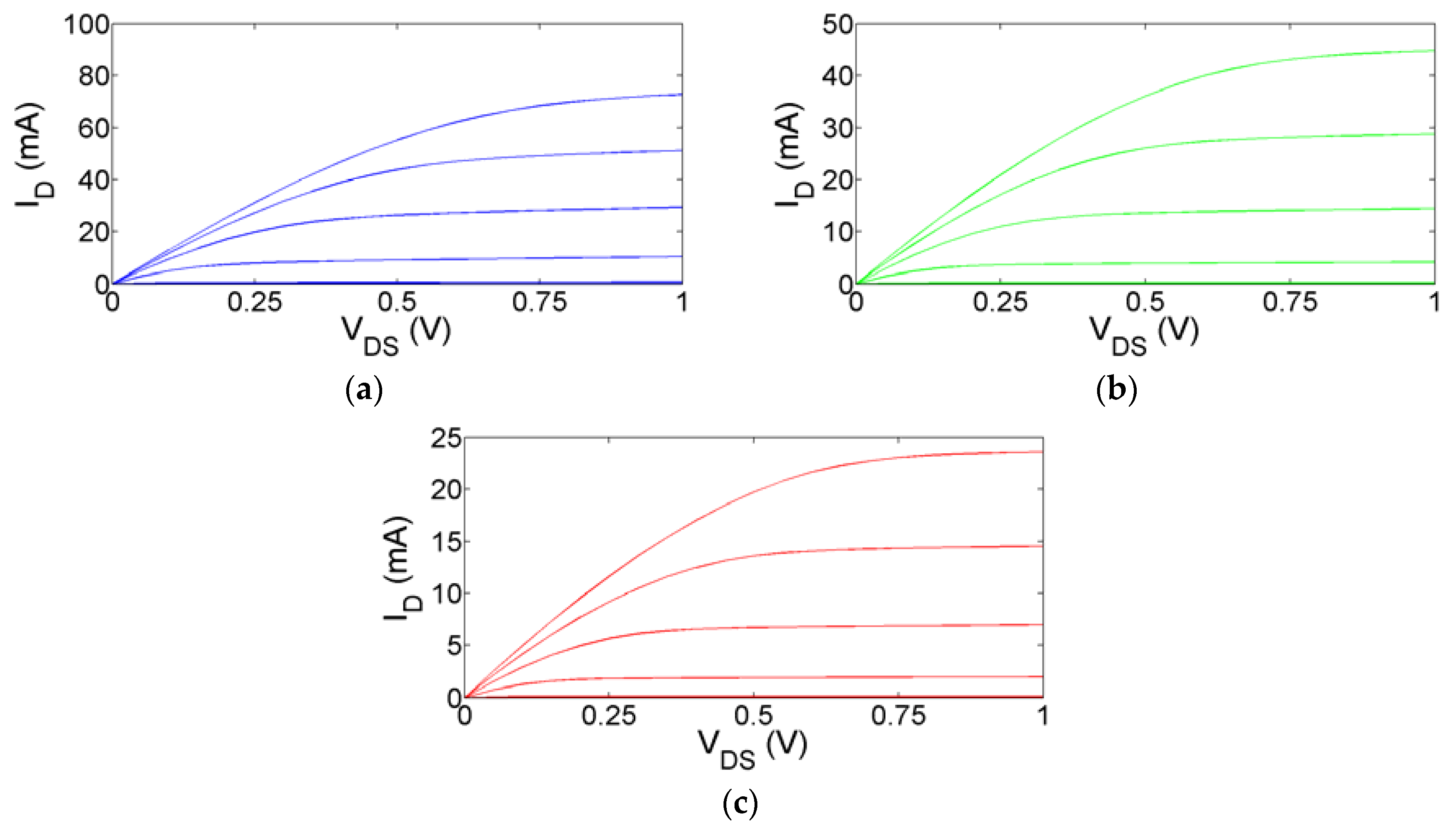
Figure 2.
Behavior of (a) ID; (b) gmExtrDC; and (c) gmDC versus gate length for three MOSFETs at VDS = 1 V and VGS = 1 V.
Figure 2.
Behavior of (a) ID; (b) gmExtrDC; and (c) gmDC versus gate length for three MOSFETs at VDS = 1 V and VGS = 1 V.

Figure 3.
Small-signal equivalent circuit for the tested MOSFETs.
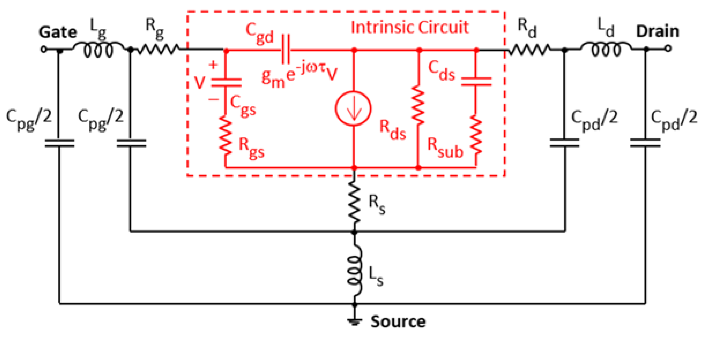
Figure 4.
Behavior of Im(Yij) versus ω for the open structure. The extracted extrinsic capacitances are: Cpg = 338 fF and Cpd = 335 fF.
Figure 4.
Behavior of Im(Yij) versus ω for the open structure. The extracted extrinsic capacitances are: Cpg = 338 fF and Cpd = 335 fF.

Figure 5.
Behavior of Re(Zij) versus 1/(VGS − VTH) for a MOSFET with a gate length of 0.25 μm at VDS = 0 V. The extracted extrinsic resistances are: Rg = 1.9 Ω, Rs = 1.7 Ω, and Rd = 2 Ω.
Figure 5.
Behavior of Re(Zij) versus 1/(VGS − VTH) for a MOSFET with a gate length of 0.25 μm at VDS = 0 V. The extracted extrinsic resistances are: Rg = 1.9 Ω, Rs = 1.7 Ω, and Rd = 2 Ω.

Figure 6.
Behavior of ωIm(Zij) versus ω2 for a MOSFET with a gate length of 0.25 μm at VDS = 0 V and VGS = 1.4 V. The extracted extrinsic inductances are: Lg = 26.6 pH, Ls = 4.3 pH, and Ld = 19.5 pH.
Figure 6.
Behavior of ωIm(Zij) versus ω2 for a MOSFET with a gate length of 0.25 μm at VDS = 0 V and VGS = 1.4 V. The extracted extrinsic inductances are: Lg = 26.6 pH, Ls = 4.3 pH, and Ld = 19.5 pH.

Figure 7.
Measured (solid colored lines) and simulated (dashed black lines) S-parameters from 0.3 to 40 GHz at VDS = 1 V and VGS = 1 V for three MOSFETs with different gate lengths: (a,b) 0.25 μm; (c,d) 0.5 μm; and (e,f) 1 μm.
Figure 7.
Measured (solid colored lines) and simulated (dashed black lines) S-parameters from 0.3 to 40 GHz at VDS = 1 V and VGS = 1 V for three MOSFETs with different gate lengths: (a,b) 0.25 μm; (c,d) 0.5 μm; and (e,f) 1 μm.
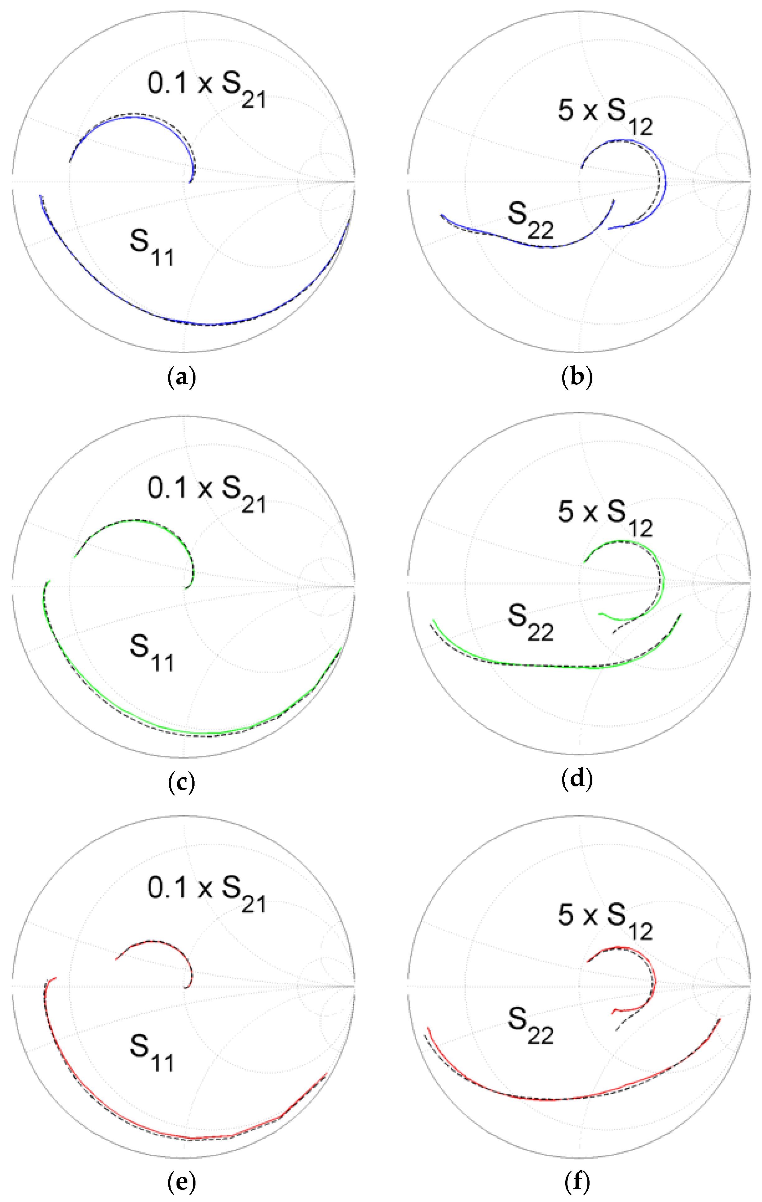
Figure 8.
Measured (solid colored lines) and simulated (dashed black lines) S22 from 0.3 to 40 GHz at VDS = 1 V and VGS = 1 V for three MOSFETs with different gate lengths: 0.25 μm, 0.5 μm, and 1 μm. The simulations are performed by omitting Rsub in the model.
Figure 8.
Measured (solid colored lines) and simulated (dashed black lines) S22 from 0.3 to 40 GHz at VDS = 1 V and VGS = 1 V for three MOSFETs with different gate lengths: 0.25 μm, 0.5 μm, and 1 μm. The simulations are performed by omitting Rsub in the model.
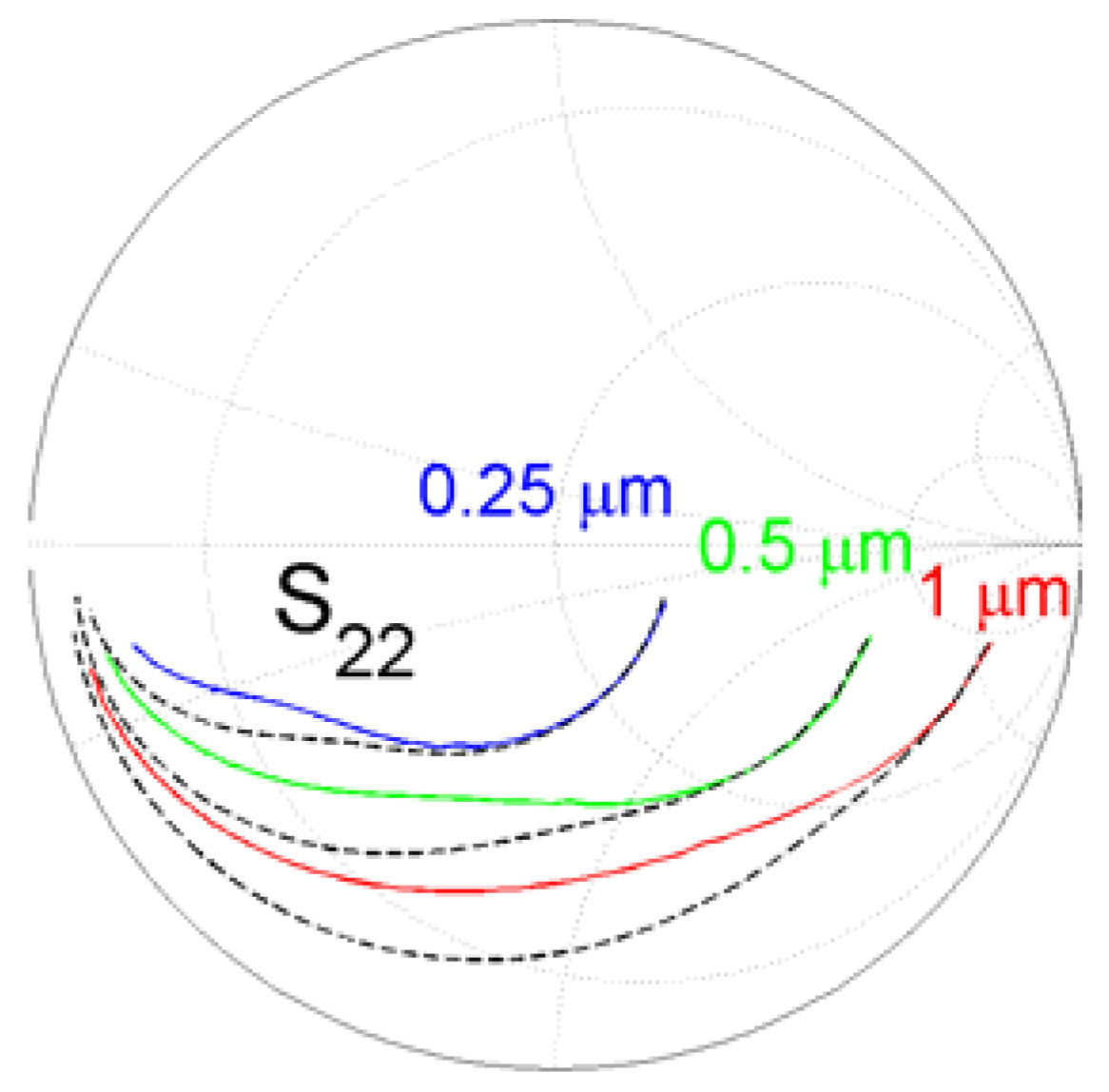
Figure 9.
Behavior of (a) gm; (b) Cgg; and (c) fT versus gate length for three MOSFETs at VDS = 1 V and VGS = 1 V.
Figure 9.
Behavior of (a) gm; (b) Cgg; and (c) fT versus gate length for three MOSFETs at VDS = 1 V and VGS = 1 V.
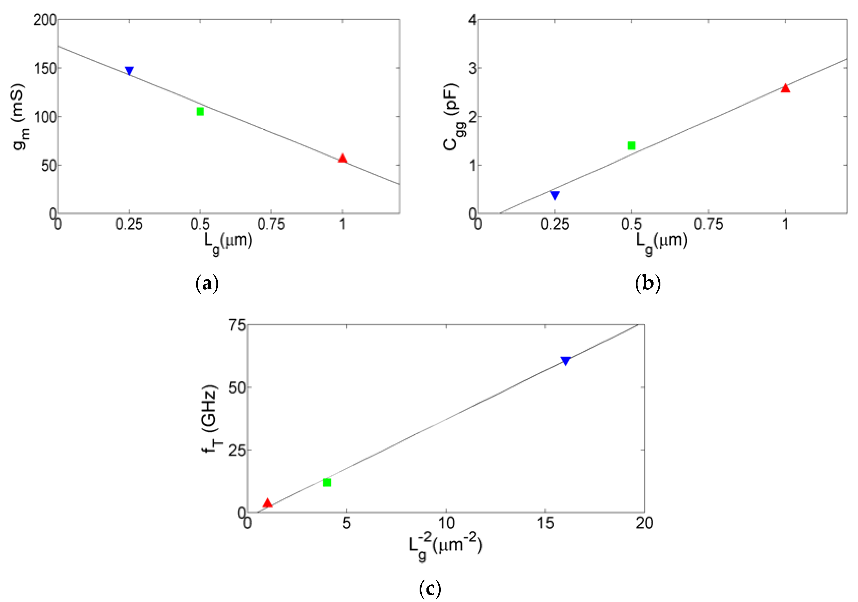
Figure 10.
Behavior of gm (colored symbols) and gmDC (white symbols) versus gate length for three MOSFETs at VDS = 1 V and VGS = 1 V.
Figure 10.
Behavior of gm (colored symbols) and gmDC (white symbols) versus gate length for three MOSFETs at VDS = 1 V and VGS = 1 V.

Figure 11.
Behavior of (a) gm; (b) Cgg; and (c) fT versus VGS for three MOSFETs with different gate lengths at VDS = 1 V.
Figure 11.
Behavior of (a) gm; (b) Cgg; and (c) fT versus VGS for three MOSFETs with different gate lengths at VDS = 1 V.

Figure 12.
Behavior of (a) gm; (b) Cg; and (c) fT versus VDS for three MOSFETs with different gate lengths at VGS = 1 V.
Figure 12.
Behavior of (a) gm; (b) Cg; and (c) fT versus VDS for three MOSFETs with different gate lengths at VGS = 1 V.
© 2017 by the authors. Licensee MDPI, Basel, Switzerland. This article is an open access article distributed under the terms and conditions of the Creative Commons Attribution (CC BY) license (http://creativecommons.org/licenses/by/4.0/).
Share and Cite
MDPI and ACS Style
Crupi, G.; Schreurs, D.M.M.-P.; Caddemi, A. Effects of Gate-Length Scaling on Microwave MOSFET Performance. Electronics 2017, 6, 62. https://doi.org/10.3390/electronics6030062
AMA Style
Crupi G, Schreurs DMM-P, Caddemi A. Effects of Gate-Length Scaling on Microwave MOSFET Performance. Electronics. 2017; 6(3):62. https://doi.org/10.3390/electronics6030062
Chicago/Turabian StyleCrupi, Giovanni, Dominique M. M.-P. Schreurs, and Alina Caddemi. 2017. "Effects of Gate-Length Scaling on Microwave MOSFET Performance" Electronics 6, no. 3: 62. https://doi.org/10.3390/electronics6030062
Note that from the first issue of 2016, this journal uses article numbers instead of page numbers. See further details here.