Efficient Fault Localization and Failure Analysis Techniques for Improving IC Yield


1
Synopsys, Mountain View, CA 94043, USA
2
Department of Electrical and Computer Engineering, University of Central Florida, Orlando, FL 32816, USA
*
Author to whom correspondence should be addressed.
Electronics 2018, 7(3), 28; https://doi.org/10.3390/electronics7030028
Submission received: 24 December 2017
/
Revised: 11 February 2018
/
Accepted: 22 February 2018
/
Published: 27 February 2018
Abstract
:With the increase in the complexity of the semiconductor device processes and increase in the challenge to satisfy high market demands, enhancement in yield has become a crucial factor. Discovering and reacting to yield problems emerging at the end of the production line may cause unbearable yield loss leading to larger times to market. Thus, time and cost involved in fault isolation may be significantly shortened by effectively utilizing the fault diagnosis technology and supporting yield improvements. Hence for yield analysis, a highly integrated data network with software analysis tools have been established to reduce the fault analysis time. Synopsys Avalon, a product used for fault localization is described in this paper which aids in achieving better integrated circuit yields. This paper also illustrates various fault localization techniques for faster problem identification and discusses a few analytical tools like photon emission microscope and transmission emission microscope for faster determination of device failures.
1. Introduction
Estimation of yield and faster yield ramp are crucial in integrated circuit (IC) manufacturing cycle. With new technologies introduced and fabricated, the yields observed could be as low as 20% of the production [1]. Thus, with 80% of the product being discarded, newer and faster schemes should be developed for detection and correction of these faults. To achieve increased yields various methods are adopted like modifying layout shapes, design rules, conditions of processes [2,3] etc. Yield ramp up thus becomes very crucial for production control, operation planning, material management and timely product delivery. Faster and accurate yield ramp forms the focal point of the industry that evolves from the production of standard products such as application specific integrated circuit (ASIC) and system on chip (SOC) products [4].
Physical defects play a crucial role in IC yields [5]. In case of complementary metal oxide semiconductor (CMOS) processes, one of the greatest loss factors of the yield is that the defect causes the electrical faults. The modeling of real defect outlines that exhibit a great variety of defect shapes is usually modeled as a circle, which causes error of critical area simulation [6,7,8]. Various new models have been experimented which can predict real defects in a much better way than the usual circular model does [9,10]. Activities for improving yield and quality by applying various analyses are conducted routinely. To increase the yield, factors that affect the process and reduce the yield are identified and the necessary countermeasures are applied to prevent their recurrence.
In the case of the memory circuit, identification of the cause of a fault is relatively easy because the address of the faulty cell can be found from test results. Therefore, the improvement of the overall yield of large scale integrated circuits as previously been attempted by analyzing the memory circuit. However, as the increases in scale and integration tend to increase the weight of the logic circuit, the yield of the logic circuit typically has a greater effect on the overall yield than it previously had. Thus, the importance of performing logic circuit analyses is increased.
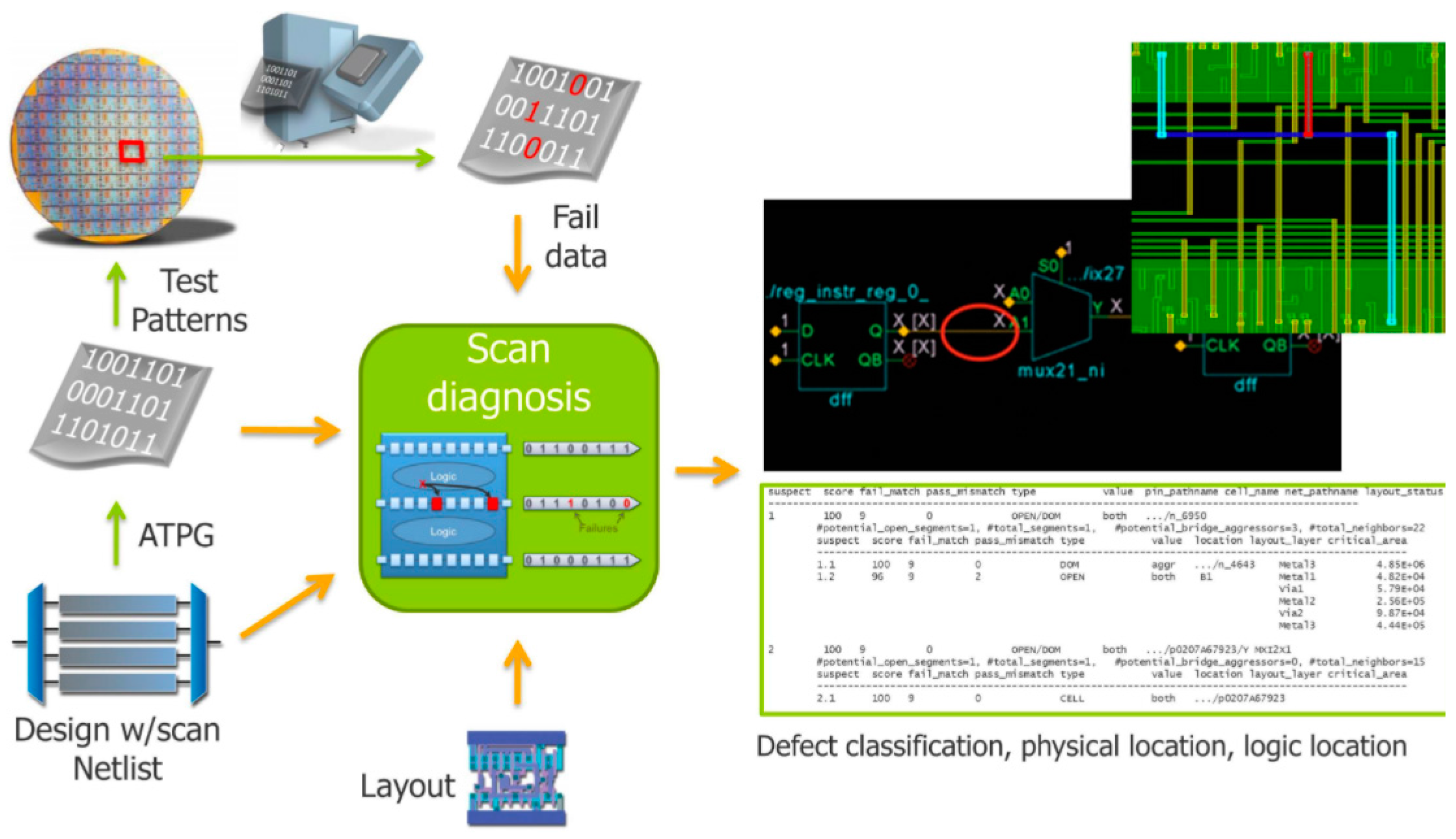
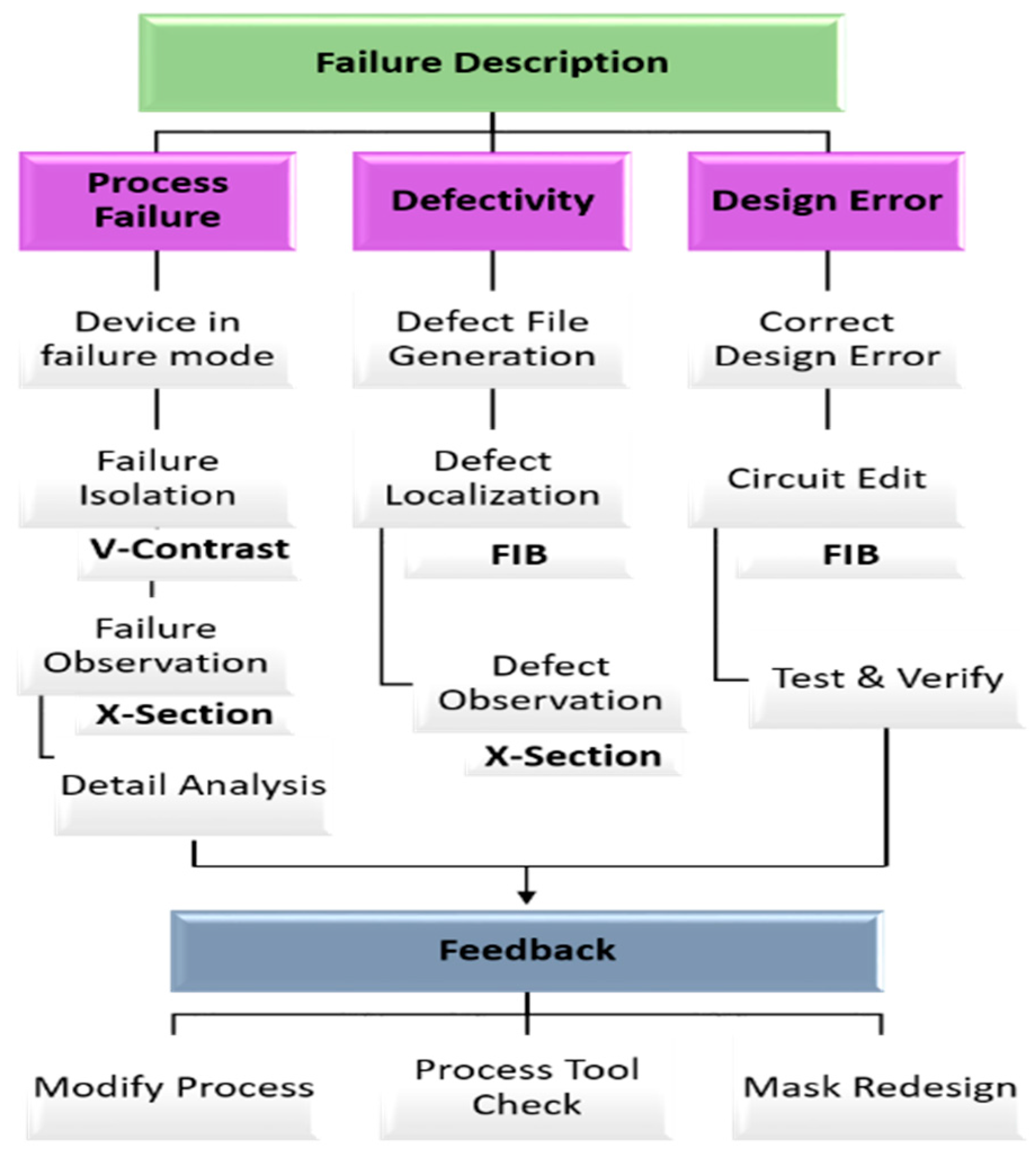
Once yield analysis is complete, failure analysis (FA) is a process to identify the root cause of failures. The FA engineers use various effective fault identification and localization techniques to localize the faulty block with high accuracy, enabling them to identify the causes of yield degradations over short periods. Failure identification is a tedious and time-consuming process. An efficient, accurate and fast analysis tool is intuitively essential to reduce IC design and/or process faults and thus improves IC yield. Synopsys’s Avalon is a tool that improves design debug accuracy and reduces root cause analysis time for yield limiters [11]. Avalon as a tool is an effective tool for fault localization. The tool also offers powerful debug capabilities for failure analysis at advanced technology nodes [12]. Figure 1 shows the two fault diagnosis techniques, including a technique for identifying the fault sites without physical failure analysis and a technique for identifying the fault sites efficiently by assessing the cause from the diagnosis results and selecting samples to be subjected to failure analysis [13].
In this paper, Section 2 discusses the fabrication centric solutions for process and product ramp to improve yield. The detail of fault identification process flow using Avalon tool is presented. In Section 3, numerous methods of fault localization have been explained. Section 4 provides flows of physical failure analysis. The conclusion is given in Section 5.
2. Fabrication Centric Solutions for Process/Product Ramp and Production
Advanced CMOS technologies have long yield ramp up times and design cycle times. This is mainly due to ignoring the process limitations of the chip design process for achieving faster time to market. Due to this, during the yield ramp up phase, the target performance is constantly met but at the tape out phase these defects cannot be addressed in a cost-effective manner leading to longer design cycle times. To address such yield detractors, it is necessary to consider the Design for Manufacturability (DFM) techniques during the chip design phase. Figure 2 shows fabrication (FAB) centric solutions for process and product ramp production.
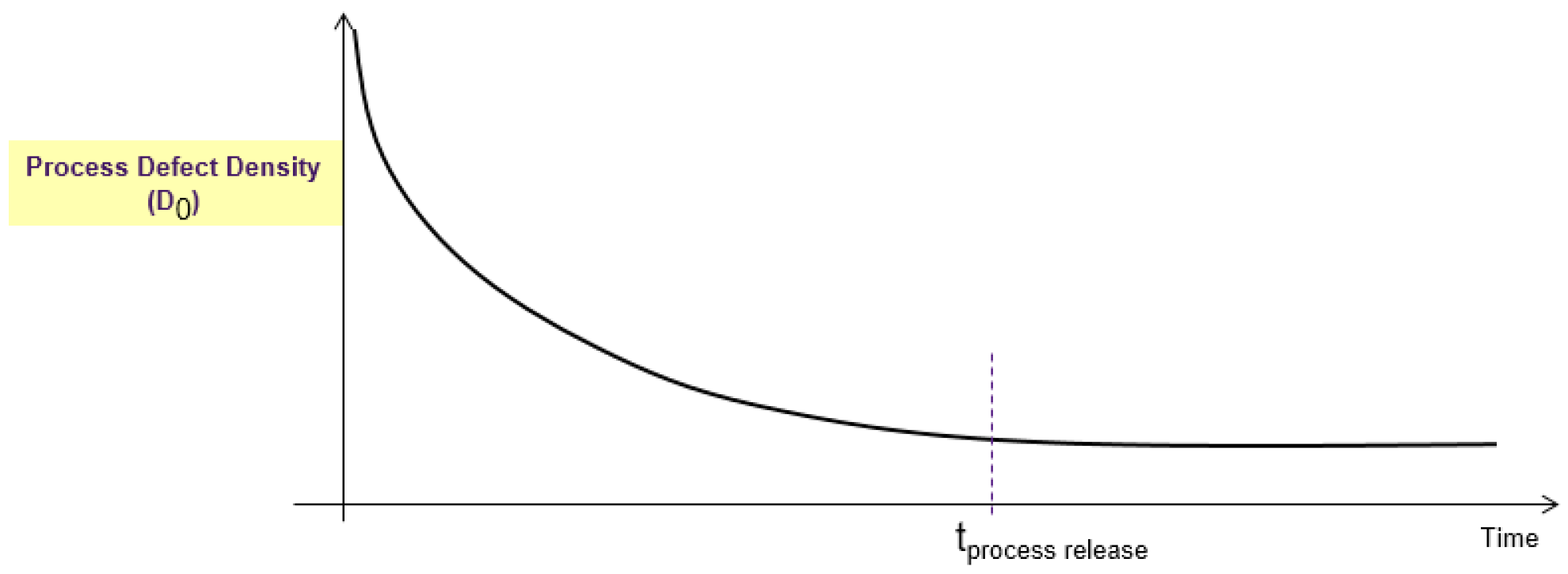
The objective of the process phase is to drive down defect density and minimize time to process-release in volume production. The main goal of process ramp is to quickly reduce the defect density to target threshold D0 as shown in Figure 3.
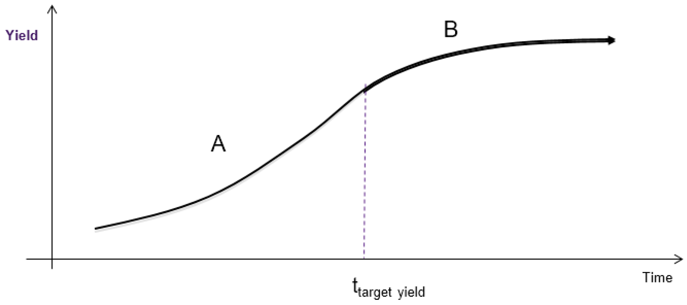
On the other hand, the objective of the new product ramp is to ramp up product yield and minimize time to product target yield. The goal of product ramp is to quickly increase the product yield to target value. Yield Explorer identifies the yield limiters arising from the design and Avalon helps confirm these yield limiters during failure analysis. In Figure 4, part A depicts the new product ramp phase. The objective in the production phase, however, is to ensure smooth production process at stable yields. Tools like Odyssey, Yield Explorer and Avalon help with maintaining these high yield levels by detecting excursions, identifying yield limiters and validating the fix. Part B in Figure 4 depicts the production phase of yield improvement.
Since the physical failure analysis (PFA) process is an expensive one, most fault candidates are filtered with very few left for the PFA. However, fault localization is a time-consuming process. A faster and accurate failure analysis helps improve the design to reduce failure rates and thus aids yield improvements. Avalon, a tool by Synopsys as a failure analysis tool, helps the FA engineer in the fault localization process [11,12]. Avalon provides easy collaboration of product and design groups with FA labs, thus improving time to yield and market. Avalon can import computer aided design (CAD) data from the key design tools and several user-proprietary formats and provides visual representations of circuits. Avalon is a power packed product with tools, features, options and networking capability that provides a complete system for fast, efficient and accurate investigation of inspection, test and analysis jobs. These features aid in the process by reducing analysis time and assisting the yield ramp. Avalon’s cross-mapping feature makes the fault identification process significantly faster.
Figure 5 shows an overview of the fault localization flow with Avalon. Avalon WaferMap integrates defect inspection data with the device CAD design using the defect coordinates to navigate an equipment stage and pinpoint the defect for closer inspection and characterization. These defects can further be cross-mapped to the layout for close inspection of the defect location on the mask layers. Suspected nets and instances can then be taken to the schematic viewer of Avalon to help determine the source and origin of the chip failures.
Avalon tool includes the following viewers to speed up the fault localization and identification process:
- MaskView—The Avalon MaskView tool can import CAD design data from all the key layout versus schematic (LVS) packages and several user-proprietary formats. It provides visual representations of circuits that can be manipulated, rotated, exploded, searched and linked with ease. It allows the tracing and cross-mapping of signals from the chip layout to netlist and schematic design data.
- NetView—Avalon NetView provides a visual representation of the net information of a chip design in the form of a hierarchical cell tree. The cell tree contains the top cell of the chip design and cell instances. The cell instances contain information on their signals and sub cells. The tool allows you to search and locate nets, cell instances and devices, cross-mapped from other Avalon tools. You can also trace and cross-map signals and cell instances from the netlist to the chip layout and schematic design data.
- SchemView—Avalon SchemView provides a pictorial representation of the chip schematic design data. The tool allows tracing and cross-mapping of signals, cell instances and devices from the schematic design to the chip layout and the netlist data.
- ISchemView—Avalon ISchemView provides a visual representation of the chip schematic design data. The tool allows tracing and cross-mapping of signals and cell instances from the schematic design to the chip layout and the netlist data. It helps in interactively viewing the desired instances/net.
- BitMap—Avalon BitMap allows you to analyze the memory layout of a chip. You can load the chip’s memory specification (memspec) files, created using Avalon MaskView, in Avalon. The tool then accepts a logical or a topological memory address and converts it to a physical address, or vice versa, using the expressions in the specification file. You can also cross-map the computed physical addresses to view them on the chip layout opened in MaskView.
- WaferMap—Avalon WaferMap provides a visual representation of the wafer under inspection, the dies present in the wafer and the defects present in the dies. The tool allows cross-mapping of defects in the wafer to their die layout opened in Avalon MaskView.
Key Avalon Features Include:
- The HotSpot Analyzer in MaskView: allows user to draw regions on the layout that correspond to hot-spot regions (emission spots) to detect the crucial nets. It finds the nets in each hot-spot region and plots a pareto graph of nets crossing one or more hotspots which helps easily locate the killer net. Figure 6 shows how CAD navigation is possible through Avalon and how Avalon HotSpot Analyzer helps in fault localization.
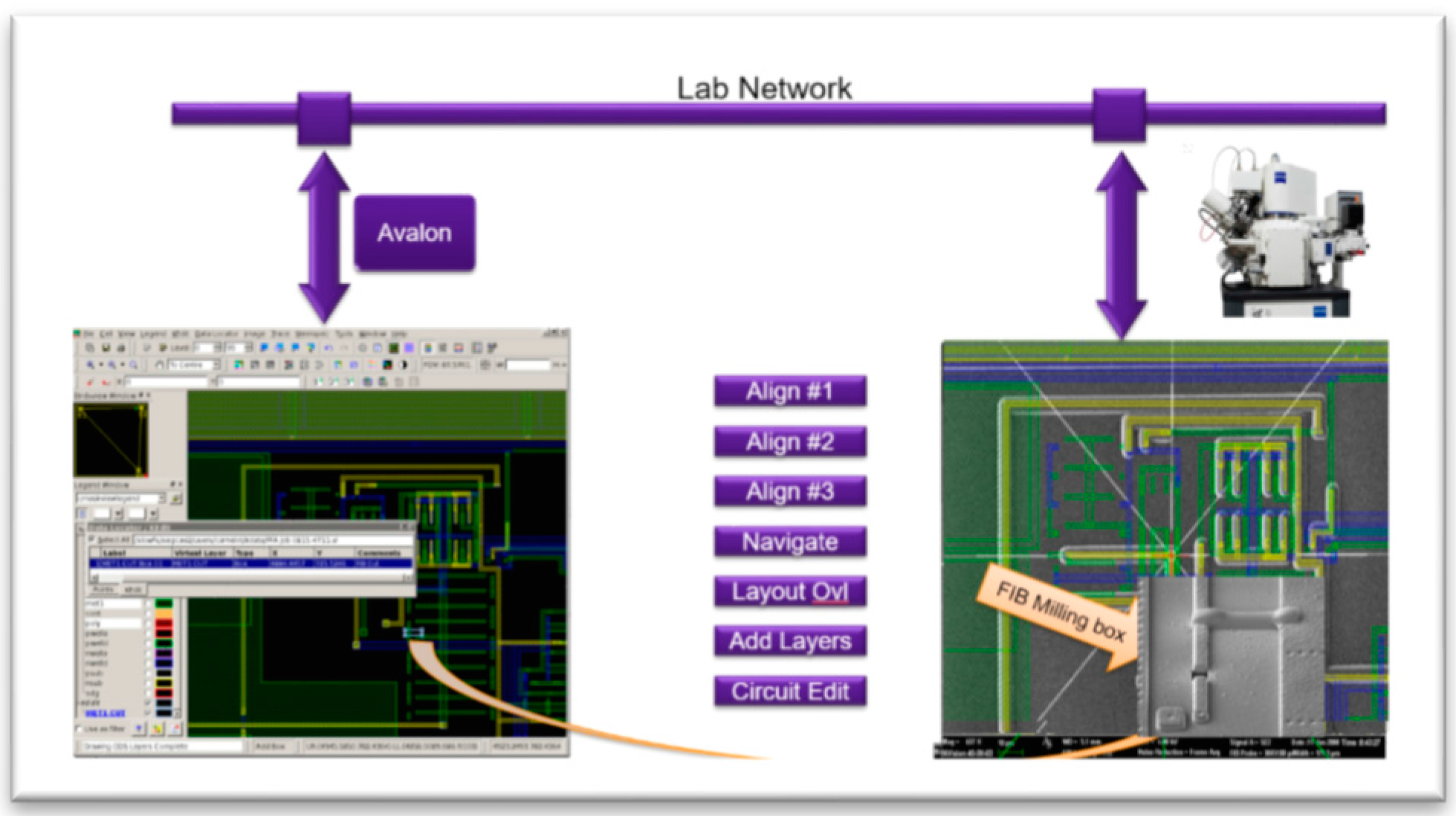
- Avalon’s capability to communicate with the equipment. Figure 7 shows the role of Avalon in PFA using its 3-point alignment and communication with manufacturing equipment.
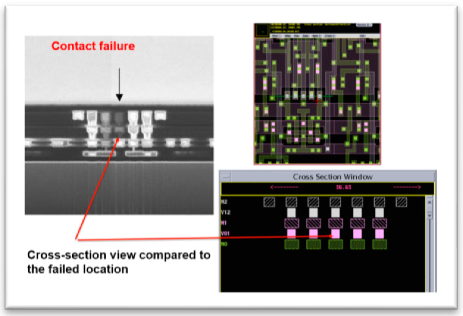
- The cross-section as viewed with the scanning emission microscope (SEM) analysis compared with the cross-sectional view of MaskView (see Figure 8).
- Image Mapper: Avalon’s capability to communicate with the FA tools for synchronization and alignment. It automates the image alignment process in Avalon MaskView and saves time and effort spent in manual alignment. The image loading feature in MaskView enhances the process of overlaying the defect candidates in the layout viewer. Figure 9 shows an image overlay in Avalon.
- Export Partial Layout: Enables the customer to share partial layout data with service labs without compromising the intellectual property (IP) of the product.
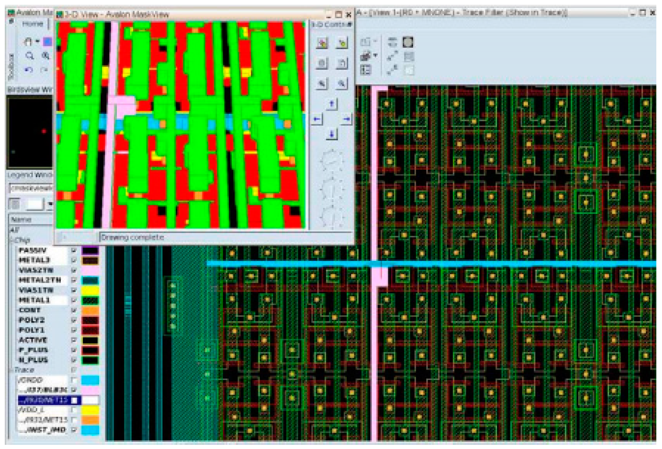
- Advanced three-dimension (3D) Viewer: Displays real time 3D view of the selected layout area. It shows each process step in the 3D view for which it uses the process data along with design data. It zooms into smaller details and helps minimize unintended consequences during focused ion beam (FIB) cuts, due to the underneath high-density structure.
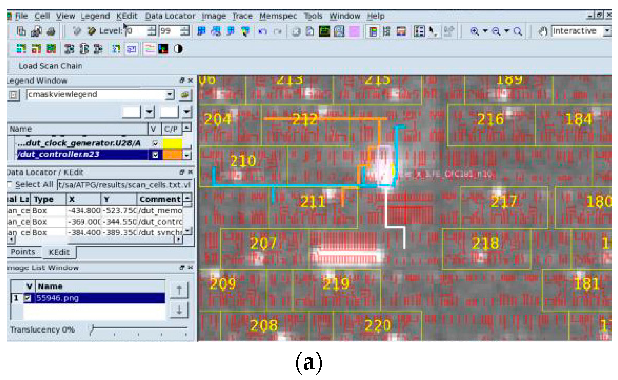
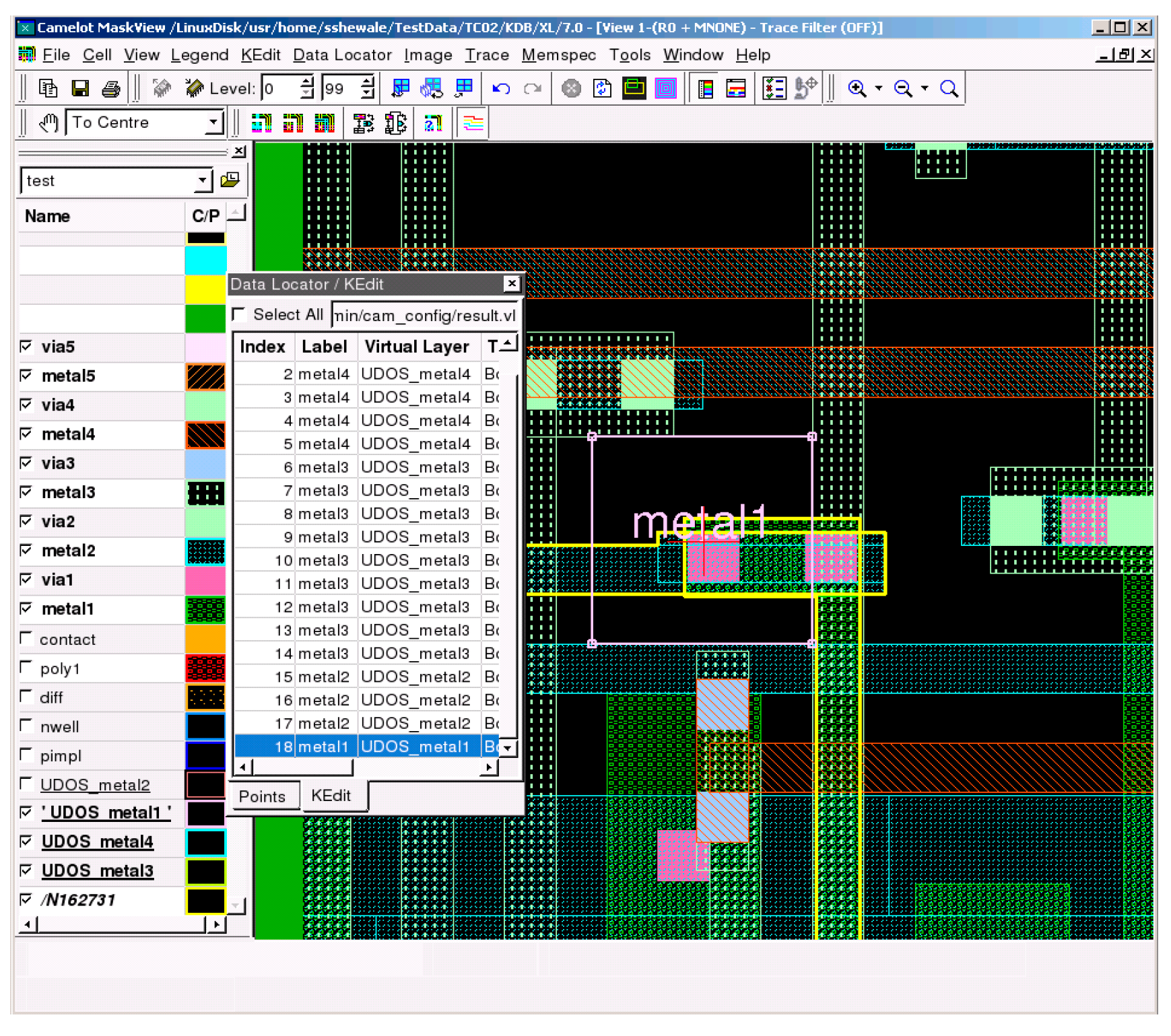
- Electronic Virtual Layer marks objects to represent net connectivity during FIB deposit or cut using KEdit (see Figure 10). The online trace will simulate the new connectivity to the virtual layer.
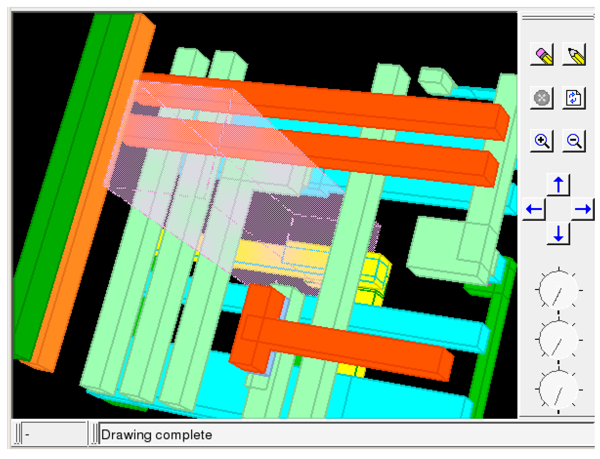
- 3D view of the layout for better visibility of the FIB simulation: provides a three-dimensional cross-section capability to FA engineers, enabling faster localization of circuit failures to accelerate IC manufacturing yield improvement. Figure 11 shows a 3D analysis that enables faster localization of circuit failures.
3. Methods of Fault Identification and Localization for Yield Improvement
In semiconductor industry, FA is crucial for improving the productivity of devices. However, the decreasing nodes, complex designs and the 3D structures complicates the failures thus making FA difficult. FA engineers spend most of their time in localizing the fault and have also found cases where fault site localization is impossible. Hence, to improve FA yield and deduce the root cause of the faulty device better fault localization techniques must be implemented [14].
Scan is one of the most commonly used Design for Test (DFT) methodologies in modern integrated circuit design. It enhances observability of faulty internal nodes of system logic during testing and is vital to product yield learning. Fundamentally, there are two parts to scan based testing. The functionality of scan chain integrity is checked prior to scan logic testing [15,16].
3.1. Software-Based Scan Chain Approach
With the software based scan chain approach, the test logs achieved which consists of the failing pins and cycles from the two tests along with the tests patterns and netlist information and inputted into a software scan diagnosis tool. These tools generate a complete diagnosis report containing information about the suspected failures and failing nodes in the circuit under test. A chain and logic diagnosis is performed to identify suspected failure sites on scan cells and system logic. To filter out the systematic fault candidates for PFA, a statistical analysis procedure follows the scan chain diagnosis [17].
3.2. Hardware-Based Scan Chain Approach
With the hardware-based Scan chain approach, an Automatic Test Equipment (ATE) interfaces with a scanning laser diagnostic tool. The ATE powers up the device and exercises the scan cells at the frequency of interest in a loop manner. Dynamic laser stimulation and photon emission is employed in fault isolation. These methodologies have greater yield success on defective scan cells, clock circuitries and selected bridging defects related to power domains. Another methodology called as frequency mapping, is a more effective approach in identifying suspected failure flops in broken chains [18].
3.3. Layout Aware Diagnosis
Combining layout data with the logic diagnosis results gives better accuracy, resolution and defect classification. Traditionally this was limited to displaying the net names only which reduces the accuracy. If such analysis is combined with the polygon information and some physical properties such as the location of the defect or the critical area, the diagnosis results become very helpful and descriptive. This a called Layout Aware Diagnosis. Layout aware diagnosis is a powerful tool for failure analysis which finds the root cause of a failing die and for yield engineers who need sets of diagnosis data to find the systematic yield limiters across the life of a product.
A. Compact Scan Test Hardware System
Advanced scan chain diagnosis is essential for better characterization and diagnosis of device under test (DUT). One of them is the Compact Scan Test Hardware System. These systems are fitted with low nose motherboard to accumulate multiple products. The system is made to utilize the same patterns of the production test which provides complete correlation with the ATE systems. The software used to drive such a hardware provides easy manipulation of conditions and patterns. The system also features diagnostic tools for the diagnosis of faults in the combinational logic or in the scan chain itself. The defect isolator tool includes features for performing comprehensive circuit and layout analysis. It takes the scan chain information, failure data, layout information and combines them all into one viewing environment. The tools used for analysis of broken chains statistically analyzes the data to determine the potential failing cells in the scan chain. The broken chain raw data is also made available [19,20].
B. Combining the Scan Test Hardware System with Traditional FA Tools and Techniques
The scan diagnosis hardware is compact enough to fit inside a photoemission and scanning laser chamber. Hence, it can easily and effectively be combined with photoemission based and scanning laser based techniques to perform dynamic fault localization.
Using a low noise and compact scan diagnosis hardware that can be fitted inside the photoemission and scanning laser chamber; unwanted delays, noise and attenuation of signals that hamper traditional setups are eliminated. There is no need for extra-long cabling often required in traditional ATE-based configuration. There is a key factor for an effective dynamic analysis while running an at-speed testing such as transitional delay. Figure 12 shows the failure analysis flow using hardware scan and diagnosis tools [21].
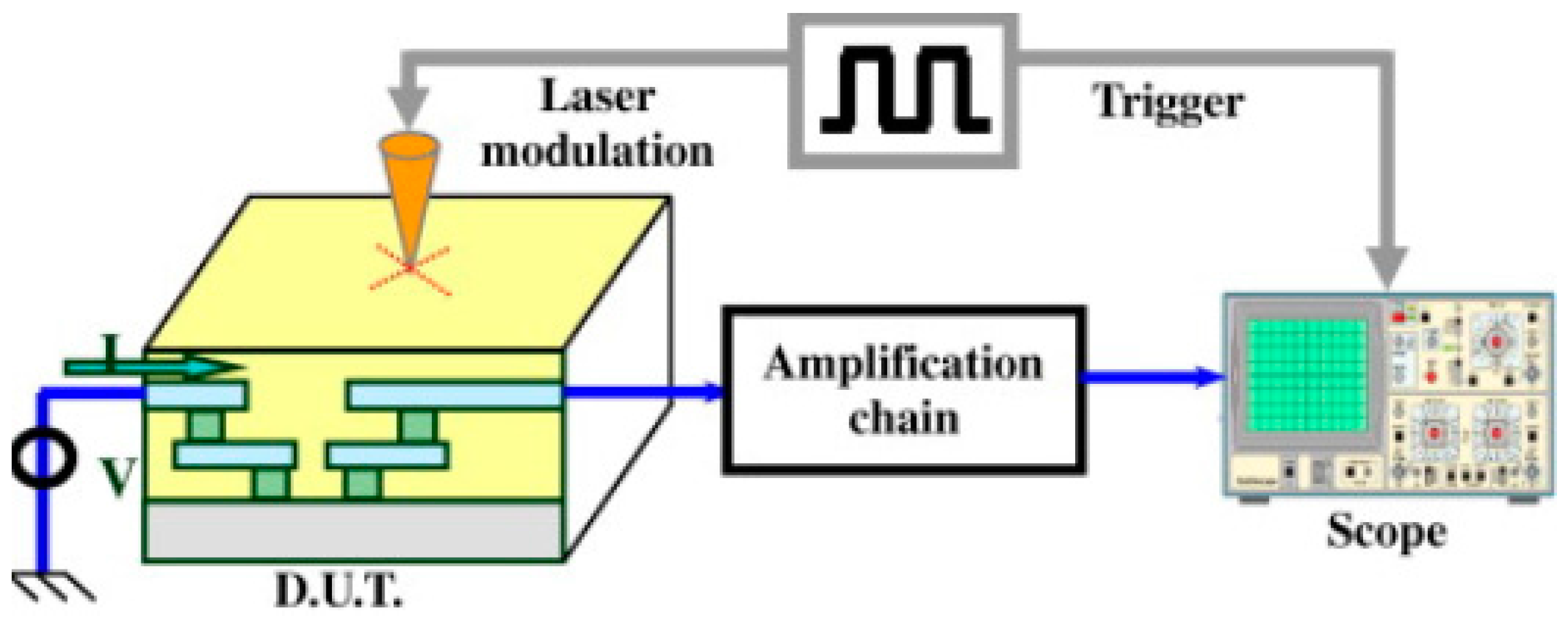
Laser-assisted device alteration (LADA) is a laser-based timing failure analysis technique (see Figure 13) used in the failure analysis of semiconductor devices [22]. The basic principle of LADA is to temporarily alter the operating characteristics of transistors on the device.
In LADA, the DUT is electrically simulated to observe the output. These techniques are mainly applied at the backside of the device to allow a direct access to the device’s active diffusion regions. On interaction of the laser with the transistor, photocurrent is generated. This photocurrent is a temporary effect and only occurs during the interaction of the laser with the target region. This photocurrent also alters the operating parameters of the transistors causing a change in its functionality. These changes can thereby alter the speed of operation of the circuit. Hence, LADA technique is used for determining the critical timing paths in a DUT.
Laser Scanning Microscope (LSM) is a powerful analytical tool that provides localized information about the microstructure of the electrical devices [22]. These tools also can connect the device under test to the diagnostics testers.
FA operation with LADA aids the FA engineer when he does not have much information or knowledge of a design. By scanning the whole design from the backside, the failed locations are detected and overlaid with silicon backside images and CAD data.
A “Shmoo” plot is a graphical display of the response of a component or system varying over a range of conditions and inputs. It is often used to represent the results of the testing of complex electronic systems, such as computers or integrated circuits such as dynamic random access memories (DRAMs), ASICs, or microprocessors. Figure 14a shows the shmoo plot for a good die while the devices are operated above 0.9 V, while Figure 14b displays the shmoo plot for a fail die while the chip fails around 0.9 V. This is what happens with the marginal failures when there are no hard failures but the performance changes with change in the parameters (voltage or frequency).
Marginal failure is common in which the failure is dependent on voltage or timing. Conventional fault isolation techniques, such as optical microscopy or electron microscopy, may be unable to isolate the fault location for marginal failure [23]. Microprobing might be able to back-trace to the faulty gate but the cycle time for probing would be significantly long and it is difficult to probe from the die top due to multi-layer metal and shrinking geometry. For such faults, we have fast dynamic fault isolation method to identify the failure location or to identify the sensitive circuitry through backside laser dynamic laser injection analysis. Instead of using conventional die top microprobing to isolate the failure location, LADA, together with modified test pattern, is used to isolate the failure location by incorporating Atomic Force Probe (AFP) and Transmission Electron Microscopy (TEM) to determine the failure [24]. In addition, LADA helps provide information about sensitive circuitry. This leads to design fixes that will overcome the marginality of failure and thus improve overall yield. Figure 15 below shows the pass/fail map using LADA corresponding to the laser scan is feedback to form the image, while the change in status in reaction to the laser indicates the failure location.
3.4. Case Study 1: Digital Circuit Failure
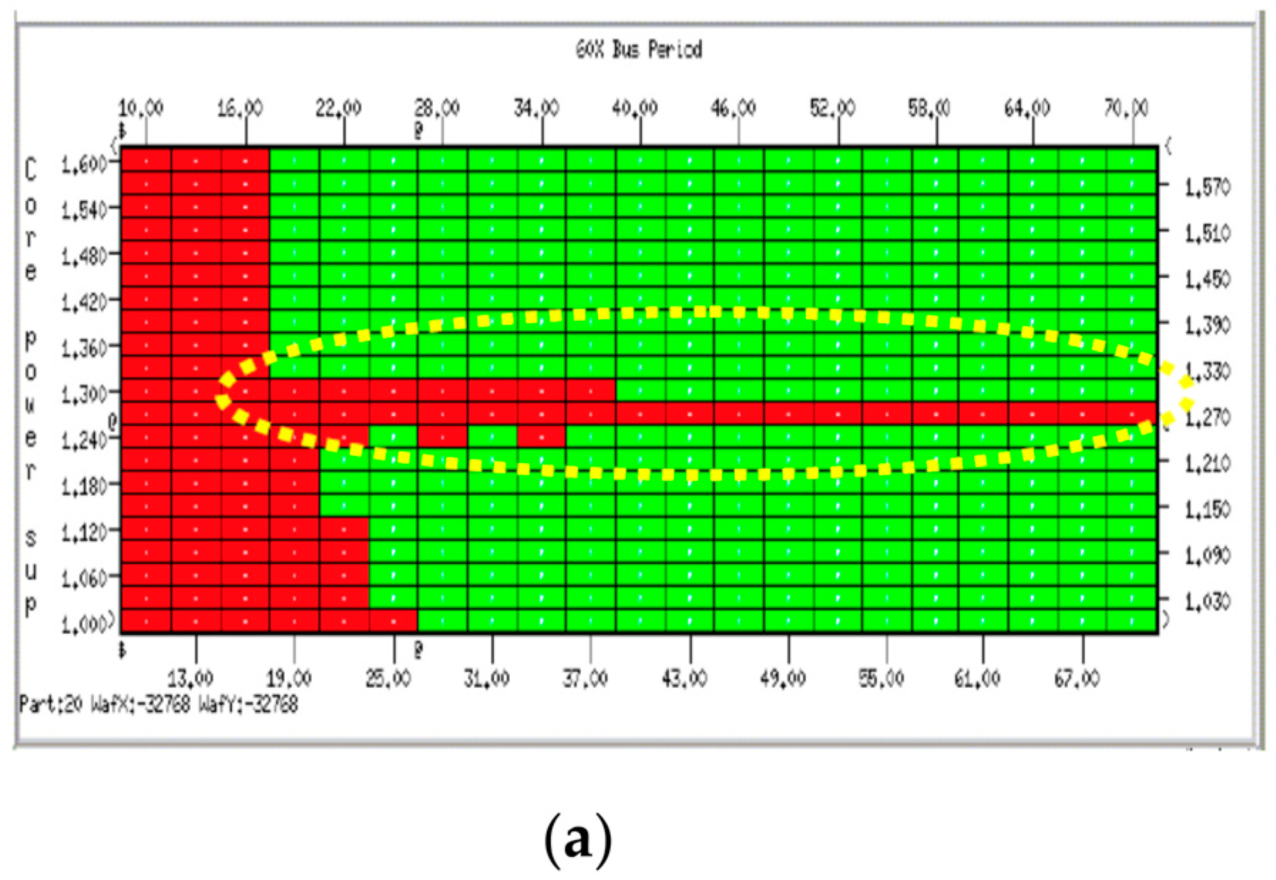
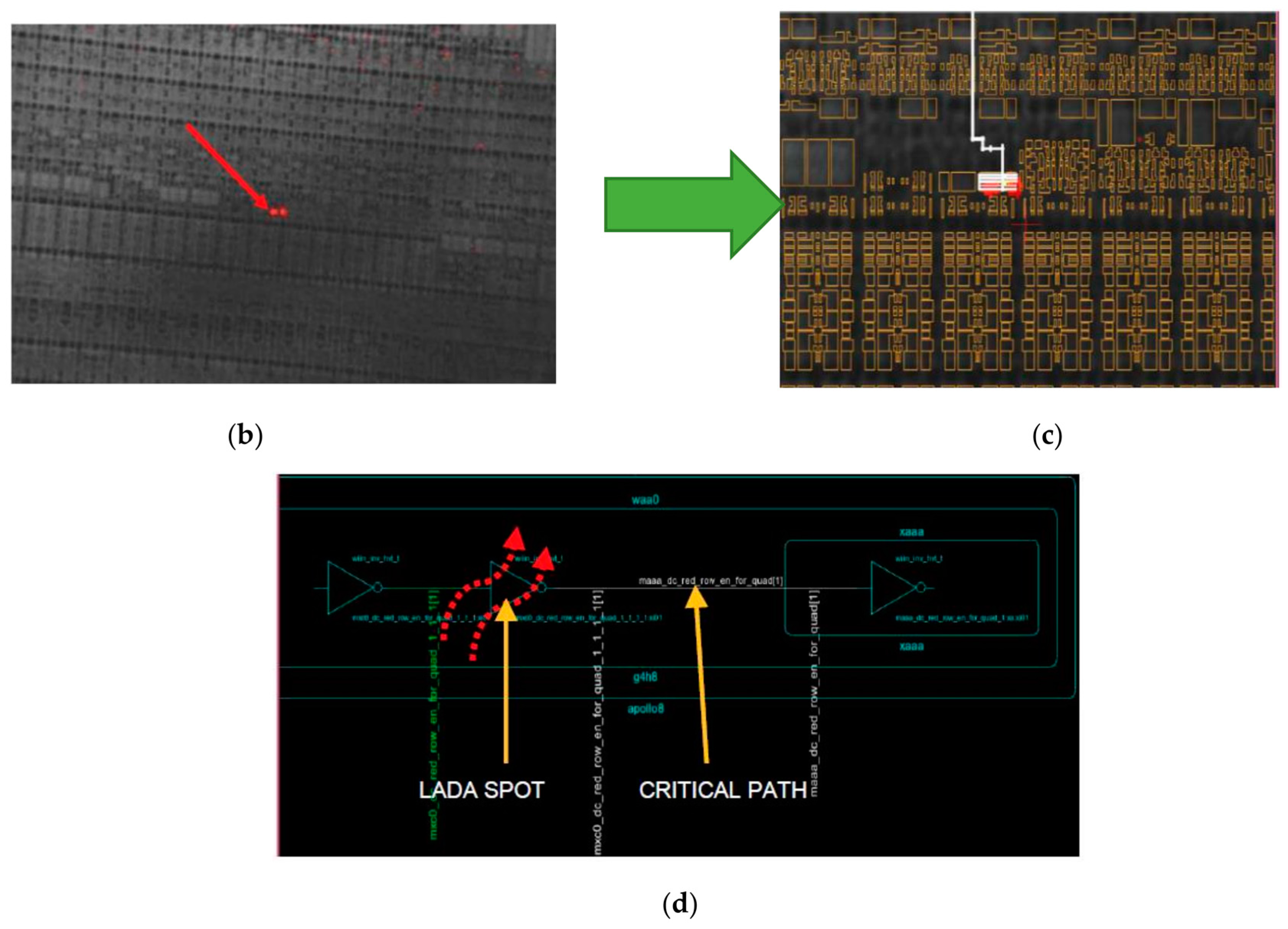
The use of LADA successfully identified the failing transistor which lead to defects without micro probing analysis from the top. The device was failing at voltages between 1.25 V and 1.30 V and passing at other voltage levels, as shown in the Shmoo plot in Figure 16a. LADA analysis was performed by setting the input near the pass region and one LADA spot was found when the laser hit the suspected faulty region and hence the faulty device. The mapping to the die layout (i.e., using MaskView—Image overlay), as shown in Figure 16b,c, and cross-mapping it to the Schematic view (SchemView) as seen in Figure 16d, revealed one critical path from fail at one of the row enable signals. This correlated with the ATE test memory failure.
3.5. Case Study 2: Scan Chain Failure
Test patterns for scan chain look quite simple, because the input data is a toggling pattern like “0011.” The output data is same as the input pattern. Inside the device, the toggling data shift through a flip-flop (F/F) chain which is synchronized to clock rising or falling. A Shmoo plot of a failing sample shows a problem at low voltage compare to that of a good sample. The output data pattern from ATE is “0111” below a certain voltage level. It is commonly known as hold violation, because the fallowing data is changed 1 cycle faster. Hold violation is simply expressed as “fast data” or “slow clock.”
The illuminated spot shows the area on the device where laser stimulation is causing the test result to change. In other words, there is sufficient device alteration to change the test result at this localized area. The LADA sensitive location is observed in the F/F cell in the MaskView as shown in Figure 17a. Through further zooming on MaskView and cross-mapping to other views, such as the Schematic View, the faulty region is identified on the clock driver as shown in Figure 17b. In this case, it appears to be a strongly localized fault.
Laser Scanning Microscope tools are powerful in defect isolation methods like Contact/Via higher resistance and metal bridge, which could be a challenge. Independently, these tools can help in various techniques like Thermally Induced Voltage Alteration (TIVA), Light Induced Voltage Alteration (LIVA) and Optical Beam Induced Resistance Change (OBIRCH). Once integrated with the device testers, these tools can also help FA engineers in Soft Defect Localization and Laser Assisted Device Alteration. In fact, hard failures are relatively easier to diagnose but for the soft defects, it is common to use the LADA methods for defect isolation.
Automatic test pattern generation (ATPG) is an automation method used to find a test pattern sequence such that when it is applied to a digital circuit, the automatic test equipment distinguishes between the correct behavior and the faulty behavior caused by defects. The patterns generated by the ATPG tools are thereby used to test semiconductor devices during and after the manufacture, to assist in determining the cause of failure. The effectiveness of ATPG is measured by the number of defects detectable by the generated patterns. These metrics generally indicate test quality (higher with more fault detections) and test application time (higher with more patterns). Figure 18 shows the ATPG flow of fault identification.
The ATPG process comprise of two phases: Fault activation and Fault propagation. Fault activation establishes a signal value at the fault model site that is opposite of the value produced by the fault model. Fault propagation moves the resulting signal value, or fault effect, forward by sensitizing a path from the fault site to a primary output.
Fault models include:
- Stuck at Fault models: In this model, one of the signal lines in a circuit is assumed to be stuck at a fixed logic value either 0 or 1. If a node, regardless of what inputs are supplied to the circuit always remains at logic 1 or 0, it is referred to as stuck at 1 or stuck at 0 fault regardless of what inputs are supplied to the circuit.
- Transistor Faults: This model is used to describe faults for CMOS logic gates. At the transistor level, a transistor maybe stuck-short or stuck-open. In stuck-short, a transistor behaves as it is always conducting (i.e., stuck at the ON state) and stuck-open is when a transistor never conducts current (or stuck-off). Stuck-short will produce a short between VDD and VSS.
- Bridging Faults: A short circuit between two signal lines is called bridging faults. Bridging to VDD or VSS is equivalent to stuck at fault model.
- Open Faults: In an open fault a wire is assumed broken and one or more inputs are disconnected from the output that should drive them. As with bridging faults, the resulting behavior depends on the circuit implementation.
- Delay Faults: Delay faults can be of different types like the Gate delay fault, Transition fault, Hold Time fault, Slow/Small delay fault, Path delay fault.
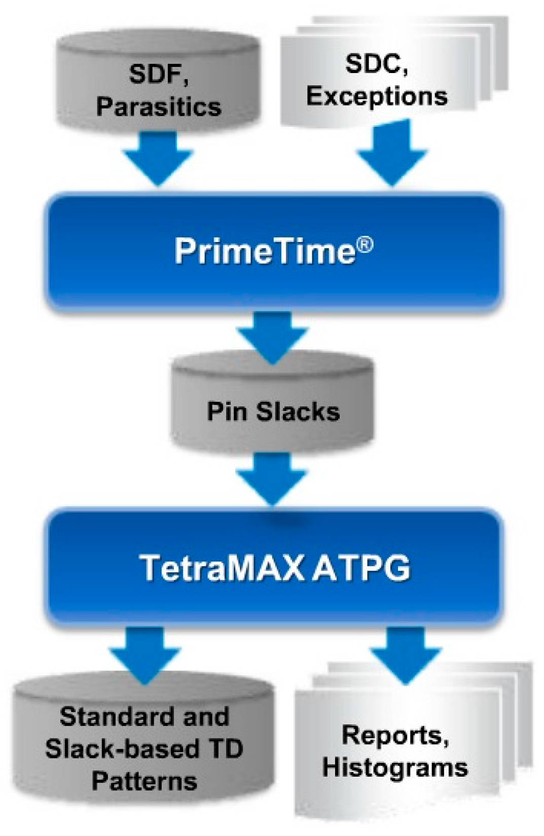
ATPG tools like TetraMax employ different fault models and tests to target each class of possible defects, such as stuck at faults, static/dynamic bridge, path delay, hold time defects etc. Figure 19 below shows a flow from the PrimeTime tool to the TetraMax ATPG tool, which helps with the detection and reporting of defects, thereby increasing yield.
These tools provide with a diagnosis reports with various information like the x, y suspected locations and the layers in the suspect segments, areas marked with defects. These files provided are compatible with most of the layout viewers. The potential candidates, after being filtered, are loaded in Avalon’s MaskView which marks the defects with the details and diagnostic result.
Voltage contrast (VC) is a commonly used isolation technique in cases where there is not any information about the circuit schematic, logic diagrams and bit maps. Hence to limit the failure analysis time for such cases voltage contrast is used as the fault localization mechanism. The primary advantage of voltage contrast over other fault localization techniques is that it is mon-destructive [25].
Four distinct ways in which voltage contrast is used in FA:
- Passive voltage contrast (PVC)
- Biased voltage contrast
- Capacitive-coupled voltage contrast
- Electron beam probing.
Passive voltage contrast uses the charge injection of the electron beam to either charge a conductor positively or negatively at low accelerating voltages that are between 500 V and 2 kV. A floating conductor such as an unconnected polysilicon gate acquires a voltage potential similar to that of the beam. For instance, if the beam charges the gate negative, the gate appears brighter in the image because it emits more secondary electrons to achieve equilibrium. A polysilicon gate with a defect, such as a short to the substrate, produces a dark contrast because the conductor does not charge negatively. Thus, the conductor emits fewer secondary electrons. Passive voltage contrast is a valuable technique for locating shorted gates, single bit floating gate memory failures and open interconnect [26].
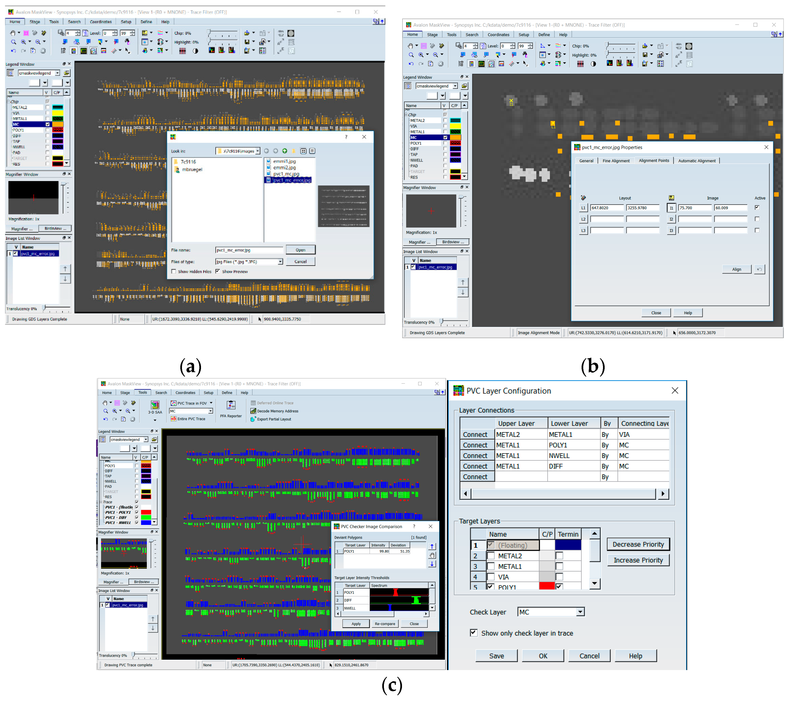
Passive Voltage Contrast is a powerful technique utilizing a Scanning Electron Microscope to identify faults on integrated circuits. It involves layer-by-layer de-processing (i.e., de-layering) and inspection of an IC on SEM. Circuit nodes are examined for anomalous states of PVC due to defect on silicon. The expected PVC states of circuit nodes are derived from design layout with knowledge of its vertical connectivity through various conducting and via layers to substrate (see Figure 20).
3.6. Wafer Navigation
Wafer testing is a step performed during semiconductor device fabrication [27]. During this step, which is performed before a wafer is sent to die preparation, all individual integrated circuits that are present on the wafer are tested for functional defects by applying special test patterns to them. Wafer testing is done by test equipment called a wafer prober. A wafer prober is a machine used to test integrated circuits. Figure 21 shows a flow of FA with wafer analysis.
As the complexity of semiconductor device processes continues to grow and the challenge to satisfy higher market demands intensifies, the establishment of the yield enhancement system has become one of the most crucial factors for contemporary fabs. There are normally four major yield loss mechanisms in wafer processing:
- Process integration issues
- Process induced defects (PID)
- Random particle from equipment and environment
- Device design problems.
Yield enhancement strategy is the ability to link together process defectivity data, electrical probe results and analytical tools to provide rapid in-line diagnostics, yield prediction and failure analysis.
Analytical tools, such as SEM and FIB, use the in-line defect coordinate information to drive straight to the defects of interest and help determine the cause of device failures. The capability of coordinate transfer between in-line inspection tools and analytical tools has proven to be a revolutionary feature for defect failure analysis. Final probe bitmapping information is converted to KLA format (binaries like “bmdb2kla” are used to convert into the KLA files which is loaded into the Avalon WaferMap application) and transferred to the analysis tool [28]. By overlaying the in-line inspection data with failed bitmap bits at wafer level, the locations of killer defects are identified.
4. Use Flows of Physical Failure Analysis
The first Dual-Beam system dedicated to defect analysis was introduced in 1998. Since then, the tool has become an industry-standard instrument in semiconductor failure analysis for Circuit Edit, Cross-Sectioning and Voltage Contrast. As the name “Dual-Beam” suggests, the system incorporates two columns—a Focused Ion Beam and a Scanning Electron Microscope. The FIB column employs a focused beam of ions for deposition and ablation of materials, whereas the SEM column uses a focused beam of electrons to image the sample or device under test [29].
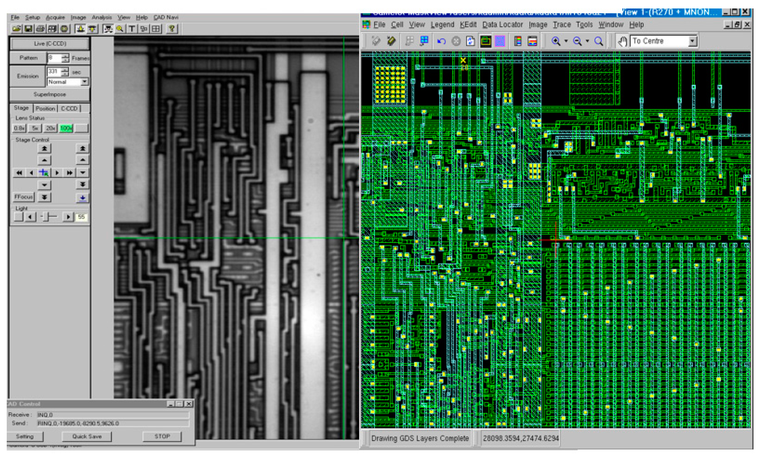
Modern-day and future FIB-SEM tools heavily depend on the software that is driving it and enabling further analysis to improve the overall yield of a product. Design-based CAD-Navigation software plays a critical role in yield improvement by getting to the failure location fast, which is one of the main challenges at sub-micron levels. Even at the accurate location, it is very difficult and sometimes impossible to see small areas of interest (such as buried tracks) and the structures surrounding it. In these cases, CAD polygons are overlaid onto the FIB image Figure 22 to visualize all the circuit features of the DUT. The CAD overlay is then used as a guide to accurately position the FIB-SEM to perform the appropriate circuit edits, cross-section, or voltage contrast [30].
Figure 23 depicts a typical FA flow, showing where the Dual-Beam is commonly used. The typical flow used with FIB-SEM and Avalon is as below:
- Volume diagnosis using tools like Yield Explorer to get potential candidates.
- Confirmation of potential candidates
- Loading and analyzing candidates in Avalon
- Using the Avalon cross-mapping feature to find failing devices/nets.
- Use the Kedit/Data locator feature to mark the desired area for correction/PFA which along with the extracted KDB for that region is sent to the FAB for the PFA.
- SEM cross-section at area of interest.
- Comparison of results: The cross-sectional view in Avalon and the actual SEM image helps view the changes/defects in the chip.
- Aligning layout and equipment
- Correction process/circuit edit (cut/deposit).
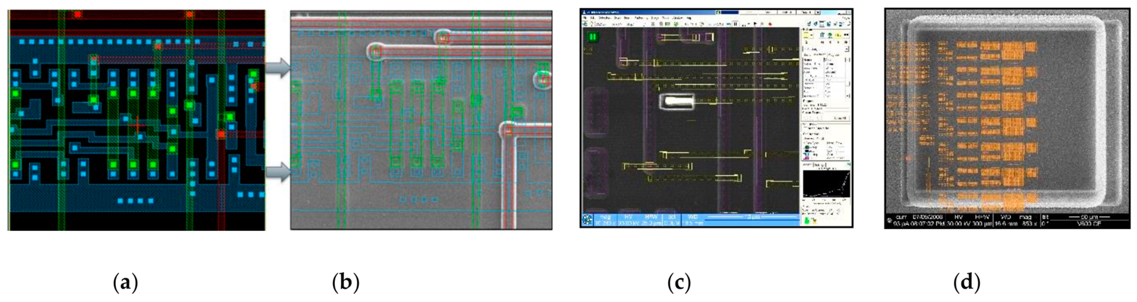
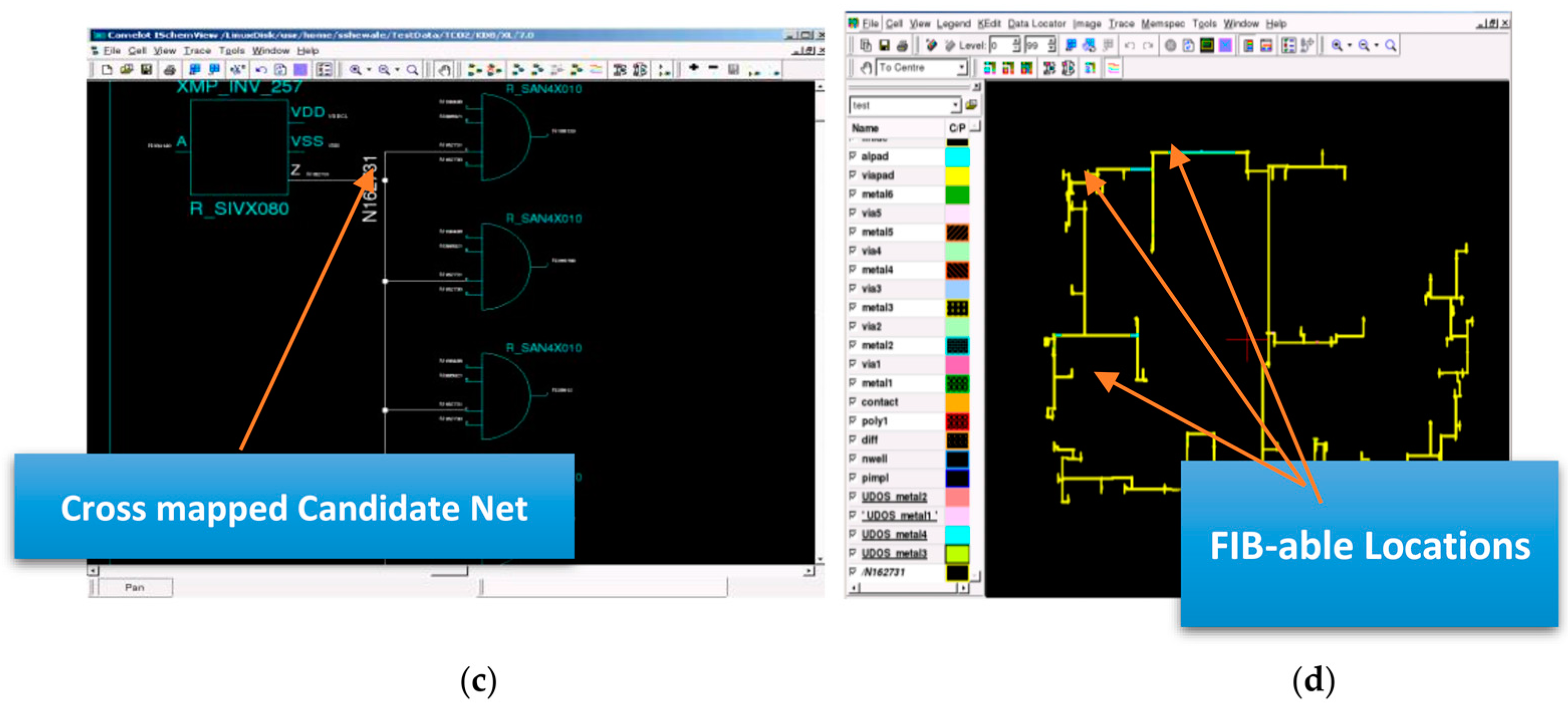
Figure 24 shows the flow with FIB. The top cell view is displayed in Figure 24a and its enlarged view is shown in Figure 24b. The candidate net is highlighted in Avalon’s Interactive Schematic as seen in Figure 24c, which shows an inverter feeding a signal into many NAND gates. Figure 24d shows the MaskView with all chip layers switched off. Traces and UDOS result overlay remain visible. This gives a high-level overview about the optimum PFA locations found on the trace. The light blue color shows the FIB locations on metal layers, which are the most qualified locations in this example.
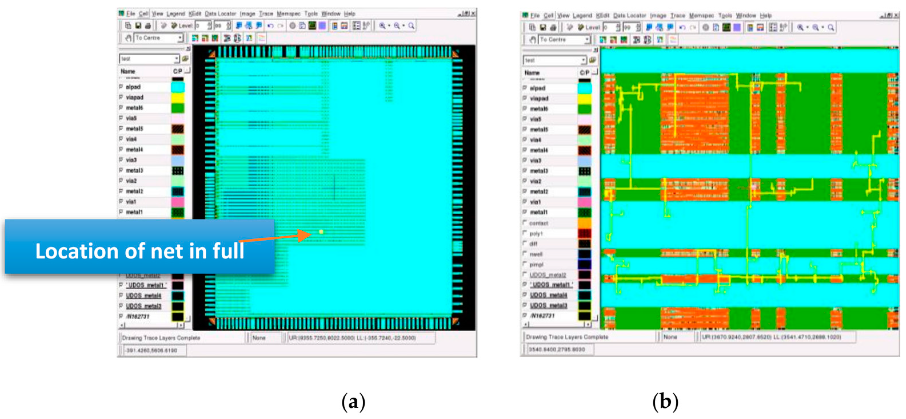
This example shown in Figure 25 shows that the UDOS search could find this single piece of Metal1 on the entire trace which is not covered by any other metal on top and has a 250 nm clearance around the metal line. Also, 3D view shown in Figure 26 gives a clear idea of the FIB task required to reach the Metal1 probe location deep in the chip. Further the layout (Avalon tool) is synchronized with the equipment to provide CAD Navigation and carry on the PFA (see Figure 27).
We now discuss some analytical tools mentioned above in more detail. Atomic Force Microscopy (AFM) is a form of Scanning Probe Microscopy where a small probe is scanned across the sample to obtain information about the sample’s surface. The information gathered from the probe’s interaction with the surface can be as simple as physical topography or as diverse as measurements of the material’s physical, magnetic, or chemical properties. Atomic force microscopy can be done in several modes using different interactions between the tip and the surface [31].
CAD navigation on AFM can help position the scan field of the AFM to the area of interest. In this case, CAD Navigation would position the wafer or the die to come close to the area to be scanned by the AFM. Conductive—Atomic force microscopy (C-AFM) is a popular failure analysis method used for localization of failures in Static Random Access Memory devices [32].
Photon emission microscopy (PEM) makes use of sensitive imaging technology in the short-wave infrared to detect the light emitted by defect sites. The corresponding die surface image (reflected light) is overlaid on the resulting emission image such that the emission spot coincides with the precise location of the defect. This allows for easy fault localization [33]. Photon emission microscopy applications include but are not restricted to, the following applications:
- Detection of avalanche luminescence from junction breakdowns, junction defects, currents due to saturated MOS transistors and transistor hot electron effects
- Detection of dielectric electroluminescence from current flow through SiO2 and SiN.
Generally, photon emissions from dies and wafers are collected from the active face or front side of the devices. However, with the increase in the number of interconnect metal layers, the probability of detecting photon emission from the front side has decreased significantly. In Backside Photon Microscopy, the emission spots are detected from the silicon backside i.e., through the silicon substrate due to the property of silicon which gets transparent to infrared light [34].
Transmission electron microscopy is a powerful analytical tool that provides localized information about the microstructure of the electrical devices. It is a form of electron microscope which derives an image from electrons that have passed through the device. The image is formed at once rather than by scanning [35,36,37,38]. TEM uses microscopy technique in which a beam of electrons is transmitted through a very thin electrical device, interacting with the device as it passes through it and generates a projection image. Due to the smaller wavelengths of electrons, TEM technology offers users much higher resolution so they can see more details than is possible with a light microscope.
Energy Dispersive X-ray Spectroscopy is based on the detection of characteristic X-rays emitted from an element because of the de-excitation of core electron holes created by a high-energy electron beam [39]. An electron from a higher binding energy electron level falls into the core hole and an X-ray with the energy of the difference of the electron level binding energies is emitted. Due to the quantization of electron energy levels, the emitted characteristic X-ray energies for elements will generally be different from element to element, with only a few spectral peaks overlapping. If the identification of one peak is ambiguous, other peaks or a limited knowledge of the sample history will often allow a reasonable elemental identification of the peak. X-ray is used in FA for elemental analysis of a sample.
5. Conclusions
Failure analysis is the process of collecting and analyzing data to determine the cause of a failure, often with the goal of determining corrective actions or liability. This paper illustrates the importance and influence of failure identification and correction for yield improvement. Fault identification becomes very critical in case of complex designs. Therefore, it is important to choose the appropriate way to reduce the potential faults and improve the overall yield of the lot.
The FA process discovers electrical and physical evidence to clearly identify the cause of failure through straightforward but sophisticated analytical measurement systems, bench top equipment and other techniques. Using appropriate equipment and work processes, the location of the failure cause is determined, isolated on the die and physically characterized. This paper lists various fault identification and localization techniques which facilitate the increase of yield. Following the fault identification, physical failure analysis is a step where the required corrective actions are performed on the failure site on the chip. This paper also talks about various PFA techniques including optical microscopy, electron microscopy, TEM and analysis using Edx/Eds.
Acknowledgments
The author (A. Oberai) would like to thank the Synopsys board of directors, research & development, quality assurance, computer aided engineering and product development groups for their precious contributions to the success of the research & product solution offering.
Author Contributions
A.O. organizes the materials and writes the manuscript. J.-S.Y. provides the technical feedback and revises the manuscript. Both authors proofread the manuscript. A.O. is a senior director at Synopsys where he is supervising the development of software product used for failure analysis.
Conflicts of Interest
The authors declare no conflict of interest.
References
- Wang, J.; Hao, Y. Yield modeling of arbitrary defect outline. In Proceedings of the 8th International Conference on Solid-State and Integrated Circuit Technology, Shanghai, China, 23–26 October 2006. [Google Scholar]
- Rencher, M. Physical DFY Technique Improve Yields. EE Times, March 2004. [Google Scholar]
- Asami, T.; Nasu, H.; Takase, H. Oyamatsu. In Proceedings of the IEEE/SEMI Advanced Semiconductor Manufacturing Conference and Workshop, Boston, MA, USA, 4–6 May 2004; pp. 448–452. [Google Scholar]
- Ferris-Prabhu, V. Modeling the critical area in yield forecasts. IEEE J. Solid-State Circ. 1985, 20, 874–878. [Google Scholar] [CrossRef]
- Ferris-Prabhu, V. Defect size variation and their effect on the critical area. IEEE J. Solid-State Circ. 1985, 20, 878–880. [Google Scholar] [CrossRef]
- De Vries, D.K.; Simon, P.L.C. Calibration of open interconnect yield models. In Proceedings of the 18th IEEE International Symposium on Defect and Fault Tolerance in VLSI Systems, Boston, MA, USA, 5 November 2003. [Google Scholar]
- Allan, G.; Walton, A. Efficient extra material critical area algorithms. IEEE Trans. Comput. Aided Des. Integr. Circ. Syst. 1999, 18, 1480–1486. [Google Scholar] [CrossRef]
- Allan, G.; Walton, A. Critical area extraction of VLSI devices for soft fault estimation. IEEE Trans. Semicond. Manuf. 1998, 1, 146–154. [Google Scholar] [CrossRef]
- Wang, J.; Hao, Y.; Liu, H.; Jing, M. Yield modeling based on circular defect size and a real defect rectangular degree. In Proceedings of the International Conference on Solid-State and Integrated Circuit Technology, Beijing, China, 18–21 October 2004; pp. 1104–1107. [Google Scholar]
- Hess, C.; Weiland, L. Issues on the size and outline of killer defects and their influence on yield modeling. In Proceedings of the IEEE/SEMI Advanced Semiconductor Manufacturing Conference and Workshop, Cambridge, MA, USA, 12–14 November 1996; pp. 423–428. [Google Scholar]
- Auvray, E.; Armagnat, P.; Cason, M.; Villab, E.; Jothi, M.; Brugel, M. Evolution of navigation and simulation tools in failure analysis. In Proceedings of the 27th European Symposium on Reliability of Electron Devices, Failure Physics and Analysis, Handel-Halle, Halle (Saale), 19–22 September 2016; pp. 1–8. [Google Scholar]
- Auvray, E.; Armagnat, P.; Saury, L.; Jothi, M.; Brugel, M. Effective scan chain failure analysis method. Microelectron. Reliab. 2017, 201–213. [Google Scholar] [CrossRef]
- Wang, J.; Hao, Y. Segmentation of IC real defect color images based on an LS space. Acta Electron. Sin. 2005, 5, 954–956. [Google Scholar]
- Burmer, C.; Görlich, S. Failure analyses for debug and ramp-up of modern IC’s. Microelectron. Reliab. 2016, 46, 1486–1497. [Google Scholar] [CrossRef]
- Masafumi, N. Logic LSI yield improvement analysis by means of fault diagnosis. NEC Tech. J. 2009, 4, 63–66. [Google Scholar]
- Kim, B.; Hong, J.; Han, Y. Improving yield learning by rapid electrical fault inspection and localization. In Proceedings of the International Symposium on Physical and Failure Analysis of Integrated Circuits, Singapore, 2–6 July 2012; pp. 1–5. [Google Scholar]
- Kuo, F.; Chen, Y. Yield ramp up by scan chain diagnosis. In Proceedings of the Asian Test Symposium, Taichung, Taiwan, 23–26 November 2009. [Google Scholar]
- Chen, H.; Qi, Z.; Wang, L.; Xu, C. A scan chain optimization method for diagnosis. In Proceedings of the IEEE International Conference on Computer Design, New York, NY, USA, 18–21 October 2015; pp. 613–620. [Google Scholar]
- Goh, S.; You, G.; Yeoh, B.; Chan, Y.; Chua Tey, C.; Yap, C.; Lim, T.; Fei, T.; Herrmann, T.; Ho, H.; et al. An effective broken scan chain diagnosis flow combining software and hardware solutions for systematic failures. In Proceedings of the IEEE International Symposium on Physical and Failure Analysis of Integrated Circuits, Singapore, 2–6 July 2012; pp. 1–5. [Google Scholar]
- Estores, R.; Vercruysse, P.; Villareal, K. Failure analysis enhancement by incorporating a compact scan chain diagnosis System. In Proceedings of the International Symposium on Testing and Failure Analysis, Houston, TX, USA, 9–13 November 2014; pp. 436–444. [Google Scholar]
- Pearson, S.; Campos, J.; Just, R.; Fraser, G.; Abreu, R.; Ernst, M.; Pang, D.; Keller, B. Evaluating and improving fault localization. In Proceedings of the IEEE/ACM International Conference on Software Engineering, Alamitos, CA, USA, 20–28 May 2017; pp. 609–620. [Google Scholar]
- Rowlette, J.; Eiles, T. Critical timing analysis in microprocessors using near-IR laser assisted device alteration (LADA). In Proceedings of the International Test Conference, Charlotte, NC, USA, 30 September–2 October 2003; pp. 264–273. [Google Scholar]
- Bruce, M. Laser induced techniques for microelectronic failure analysis: SDL and LADA. In Proceedings of the International Symposium for Testing and Failure Analysis, San Jose, CA, USA, 3–7 November 2013; pp. 56–63. [Google Scholar]
- Sheng, F.; Siew, R.; Mun, S.; Ting, D.; Teck, K. Laser assisted device alteration (LADA) for fault isolation and quick design in marginality failure. In Proceedings of the IEEE Symposium on Physical Failure Analysis and Integrated Circuits, Hsinchu, Taiwan, 29 June–2 July 2015; pp. 9–12. [Google Scholar]
- Rosenkranz, R. Failure localization with active and passive voltage contrast in FIB and SEM. J. Mater. Sci. 2011, 22, 1523. [Google Scholar] [CrossRef]
- Henderson, C. Passive Voltage Contrast. InfoTracks—SemiTracks Monthly Newsletter. Issue 115. November 2016. Available online: https://www.semitracks.com/newsletters/november/2016-november-newsletter.php (accessed on 10 November 2017).
- Lim, Y. Wafer Testing (1D). 3/20/13. Available online: https://uploadwikimedia.org/wikeversity/en/e/ef/SOC.1.D.Test.2013.3.20.pdf (accessed on 1 November 2017).
- Hsiung, S.; Tan, K.; Luo, J. New applications of the infrared emission microscopy to wafer-level backside and flip-chip package analyses. In Proceedings of the IEEE International Integrated Reliability Workshop, Lake Tahoe, CA, USA, 21–24 October 2012; pp. 147–150. [Google Scholar]
- Carleson, P.; Donnet, D.; Sidorov, O.; Rue, C. Delayering on advanced process technologies using FIB. In Proceedings of the IEEE International Symposium on Physical and Failure Analysis of Integrated Circuits, Singapore, 30 June–4 July 2014. [Google Scholar]
- Chen, Y.; Zhang, X. Focused ion beam technology and application in failure analysis. In Proceedings of the International Conference on Electronic Packaging Technology & High Density Packaging, Xi’an, China, 16–19 August 2010; pp. 957–960. [Google Scholar]
- Yee, P.; Sing, L. Application of atomic force microscopy in IC/discrete failure analysis. In Proceedings of the International Symposium on Physical and Failure Analysis of Integrated Circuits, Suzhou, China, 15–19 July 2013; pp. 449–454. [Google Scholar]
- Leong, H.W.; Zhang, O.; Lee, W.; Hoe, C.; Lin, R. C-AFM analysis of advanced IC on SRAM high resistance failure. In Proceedings of the International Symposium on Physical and Failure Analysis of Integrated Circuits, Singapore, 2–6 July 2012; pp. 1–3. [Google Scholar]
- Chapter 1: Introduction to Photon Emission Microscopy and Spectroscopy. Available online: scholarbank.nus.edu.sg (accessed on 10 November 2017).
- Shearer, J.; Le, L.; Yang, X.; Cleeves, M.; Meeks, A. Identification of an IDDQ failure mechanism using a variety of front and backside analytical techniques. In Proceedings of the International Symposium for Testing and Failure Analysis, Santa Clara, CA, USA, 1 October 2003. [Google Scholar]
- Lee, N.; Yong, F.; Nordin, N. TEM and chemical preferential etching analysis of protected FET leakage failure. In Proceedings of the International Symposium on Physical and Failure Analysis of Integrated Circuits, Hsinchu, Taiwan, 29 June–2 July 2015. [Google Scholar]
- Zhu, J.; Wang, Q.; Chen, C.; Neo, S.; Du, A.; Hua, Y. FIB sample preparation for TEM failure analysis of advanced devices. In Proceedings of the International Symposium on Physical and Failure Analysis of Integrated Circuits, Singapore, 5–9 July 2010; pp. 1–5. [Google Scholar]
- Stark, T.; Russell, P.; Nevers, C. 3-D defect characterization using plan view and cross-sectional TEM/STEM analysis. In Proceedings of the 31st International Symposium for Testing and Failure Analysis, San Jose, CA, USA, 6–10 November 2005; pp. 344–349. [Google Scholar]
- Soo, C.; Liu, B.; Er, E.; Zhao, S.; Lam, J.; Liu, W.; Mun, J. Study on the poly bump defect by TEM failure analysis. In Proceedings of the International Symposium on Physical and Failure Analysis of Integrated Circuits, Hsinchu, Taiwan, 29 June–2 July 2015; pp. 299–301. [Google Scholar]
- Hua, Y.; Liu, B.; Mo, Z.; Teong, J. Studies and applications of standardless EDX quantification method in failure analysis of wafer fabrication. In Proceedings of the International Symposium on Physical and Failure Analysis of Integrated Circuits, Singapore, 7–11 July 2008; pp. 1–6. [Google Scholar]
Figure 1.
Flow of failure analysis for yield improvement.
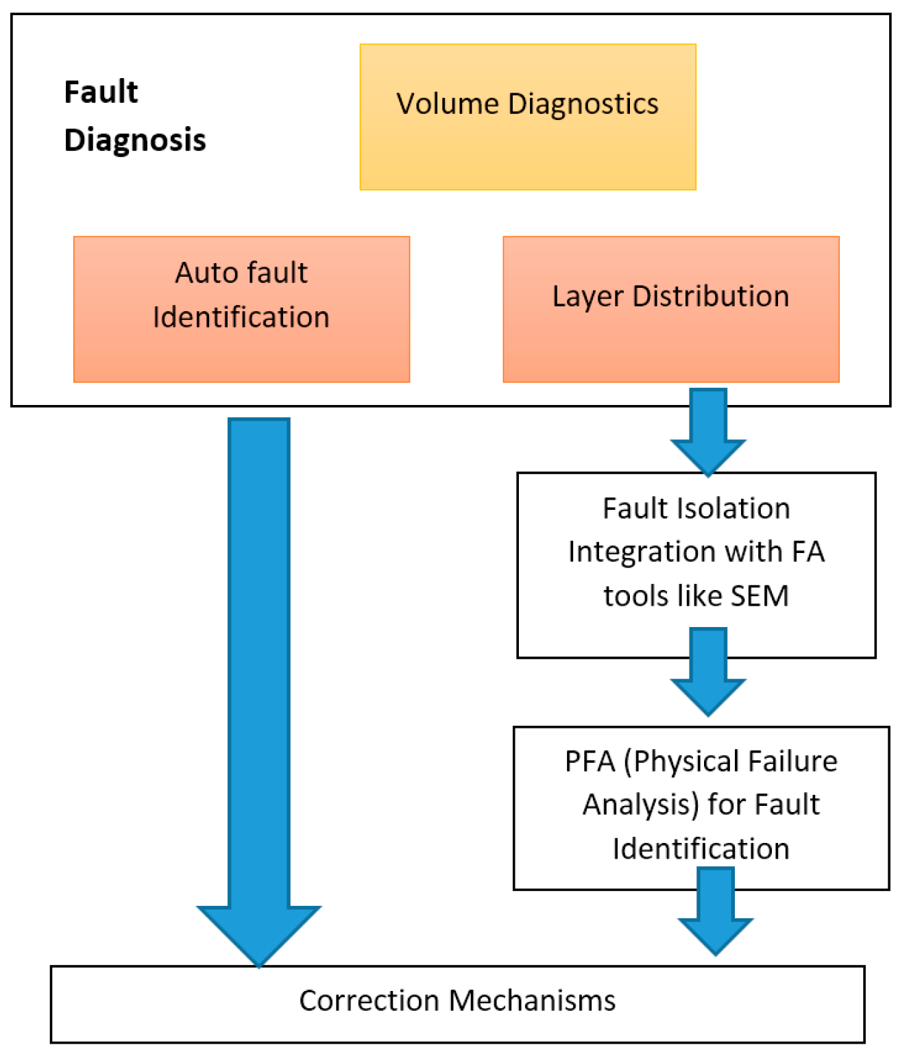
Figure 2.
Fabrication centric solutions for process/product ramp production.

Figure 3.
Graph of New Process Ramp.

Figure 4.
Graph of new product ramp and production phase.

Figure 5.
Avalon flow for fault localization.
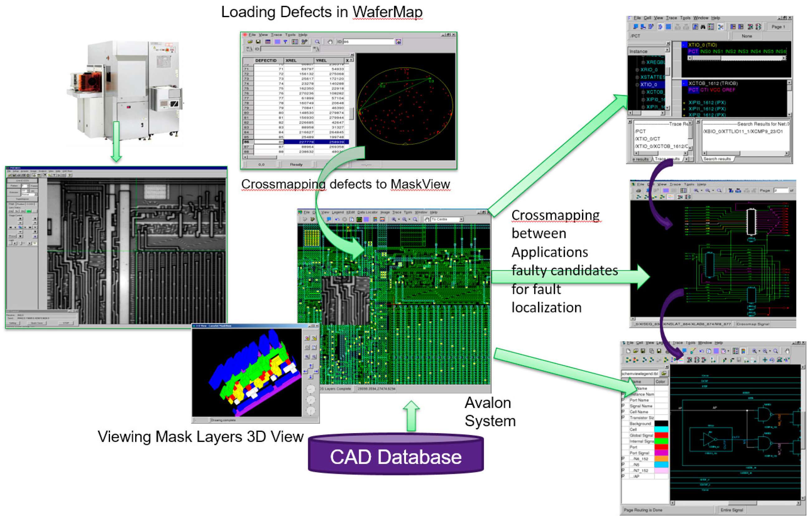
Figure 6.
Photon emission interaction with Avalon HotSpot Analyzer.

Figure 7.
CAD navigation through Avalon and equipment communication.

Figure 8.
Actual cross-sectional image compared with Avalon cross-sectional image.

Figure 9.
Image Overlay in Avalon.
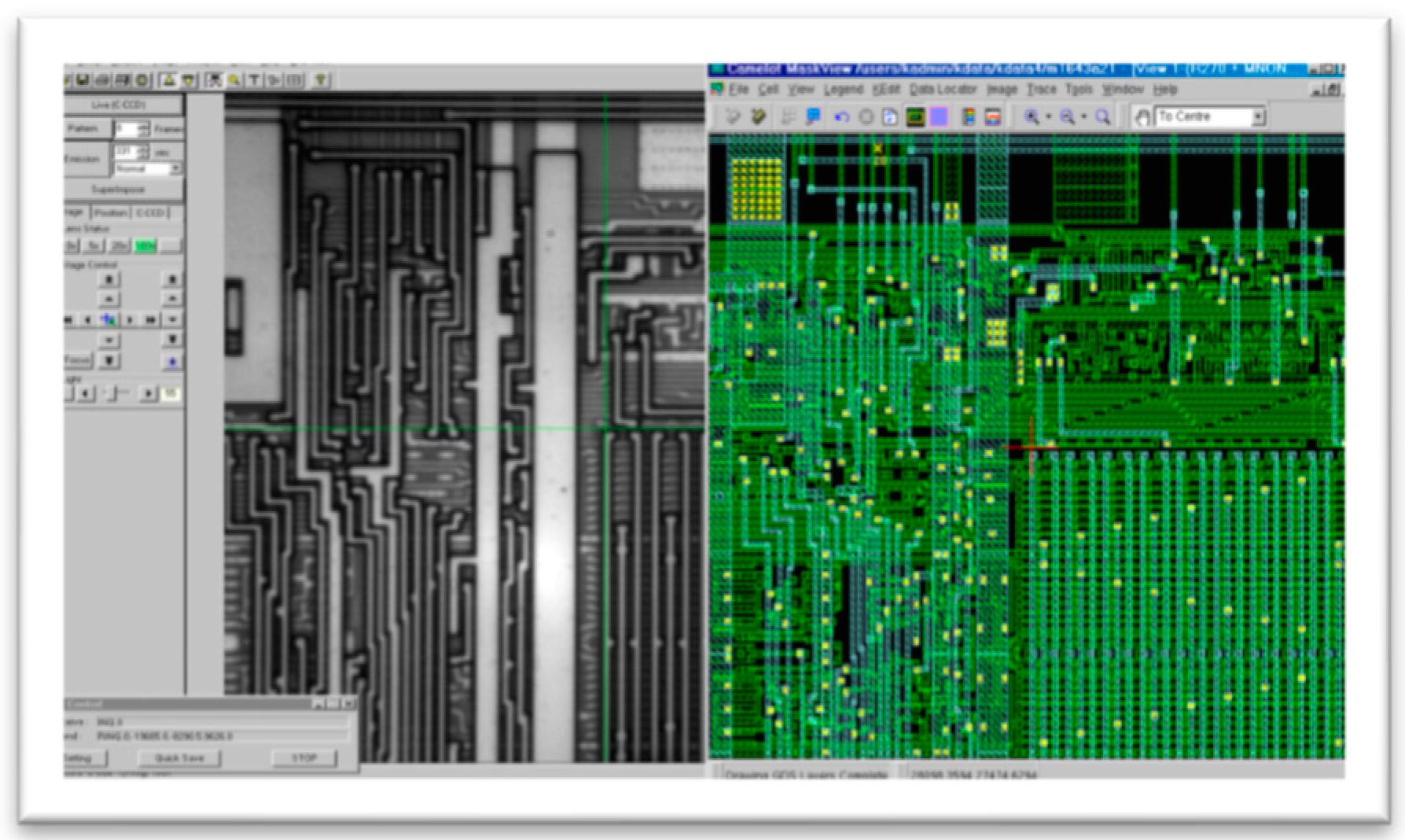
Figure 10.
Kedit box for Cut-deposit.
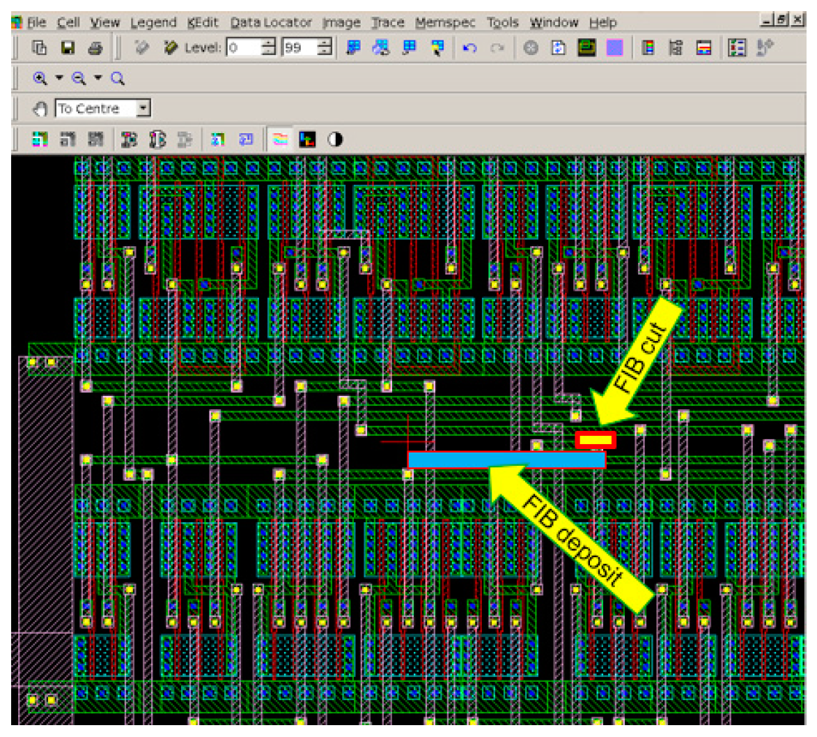
Figure 11.
3D small-area analysis to enable faster localization of circuit failures.

Figure 12.
Failure analysis flow of digital failures using compact scan hardware and diagnosis tool sets.
Figure 12.
Failure analysis flow of digital failures using compact scan hardware and diagnosis tool sets.
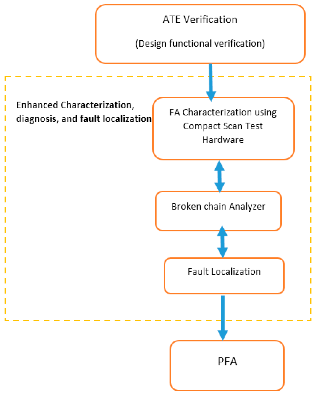
Figure 13.
Principle of laser-assisted device alternation.

Figure 14.
(a) Shmoo plot for a good die. (b) Shmoo plot for a marginal-voltage fail die.
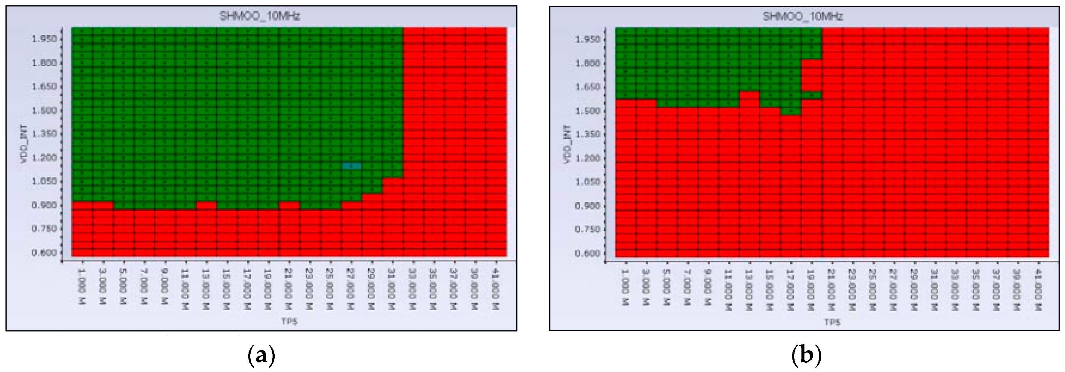
Figure 15.
The pass/fail map using LADA.
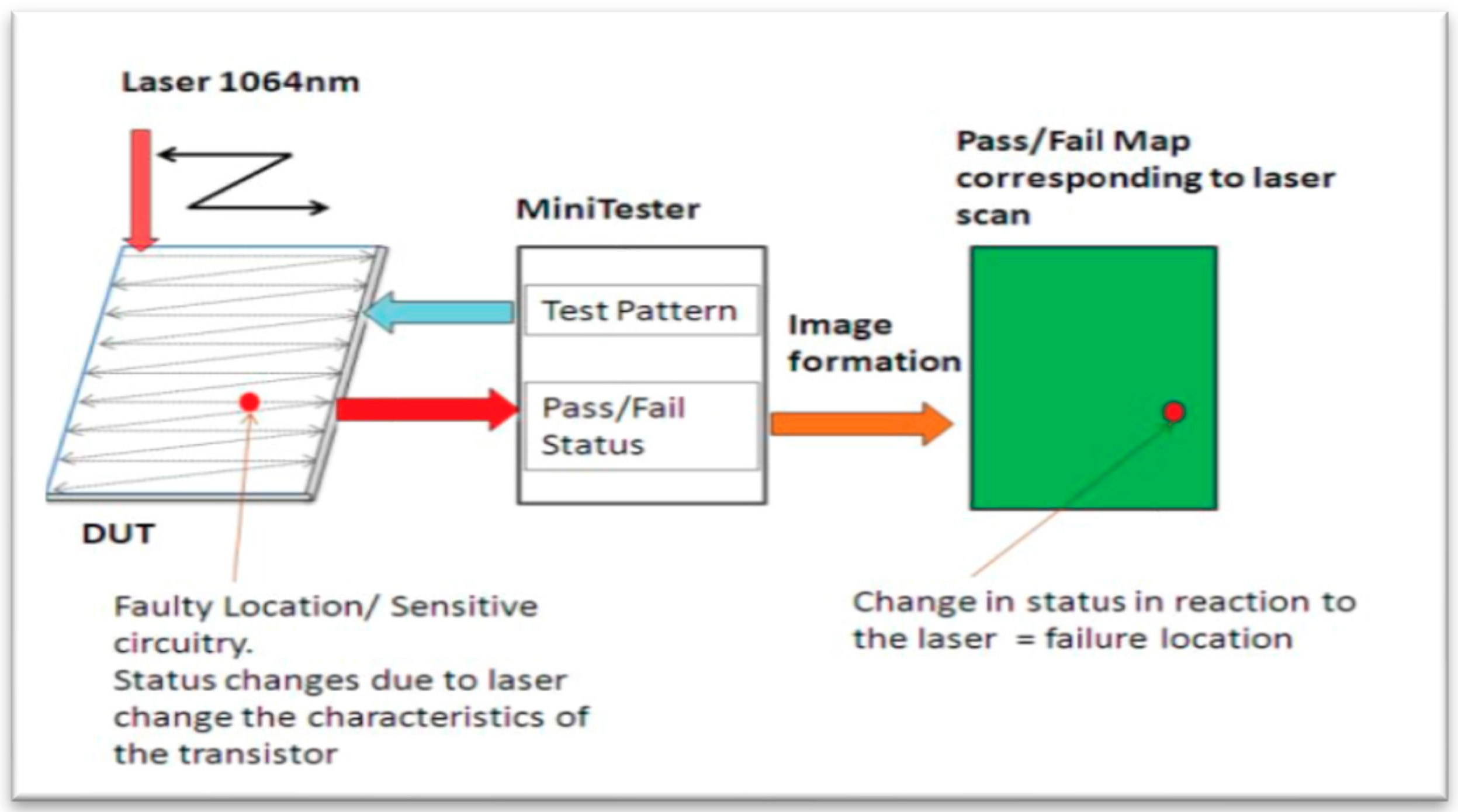
Figure 16.
(a) Shmoo plot for failure between 1.25 V–1.30 V (b) Higher magnification of the LADA spot. (c) LADA spot on layout (d) The critical path from the LADA analysis was identified at the row decoder enable signal.
Figure 16.
(a) Shmoo plot for failure between 1.25 V–1.30 V (b) Higher magnification of the LADA spot. (c) LADA spot on layout (d) The critical path from the LADA analysis was identified at the row decoder enable signal.


Figure 17.
(a) The faulty scan chain illuminated (Image overlay in MaskView) (b) Schematic view of the clock driver highlighted.
Figure 17.
(a) The faulty scan chain illuminated (Image overlay in MaskView) (b) Schematic view of the clock driver highlighted.


Figure 18.
ATPG flow of fault identification.

Figure 19.
Synopsys flow from PrimeTime to TetraMax ATPG.

Figure 20.
Use flow of PVC checker in Avalon Tool. (a) Load SEM Image Showing passive voltage contrast (b) Align Image to CAD (c) Setup PVC Checker (d) Analyzing results-finding the deviated polygons.
Figure 20.
Use flow of PVC checker in Avalon Tool. (a) Load SEM Image Showing passive voltage contrast (b) Align Image to CAD (c) Setup PVC Checker (d) Analyzing results-finding the deviated polygons.

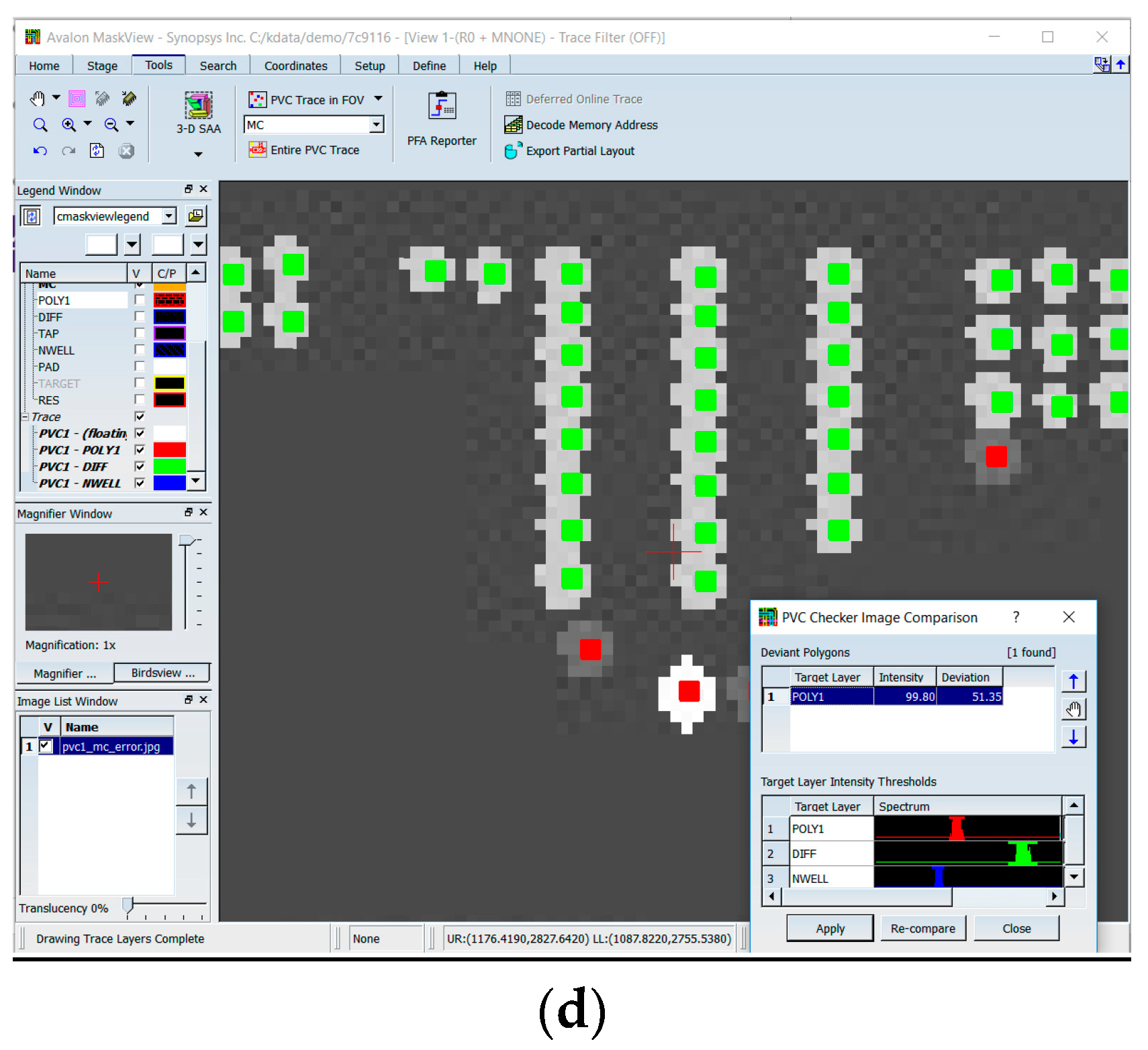
Figure 21.
General flow of FA with Wafer Analysis.
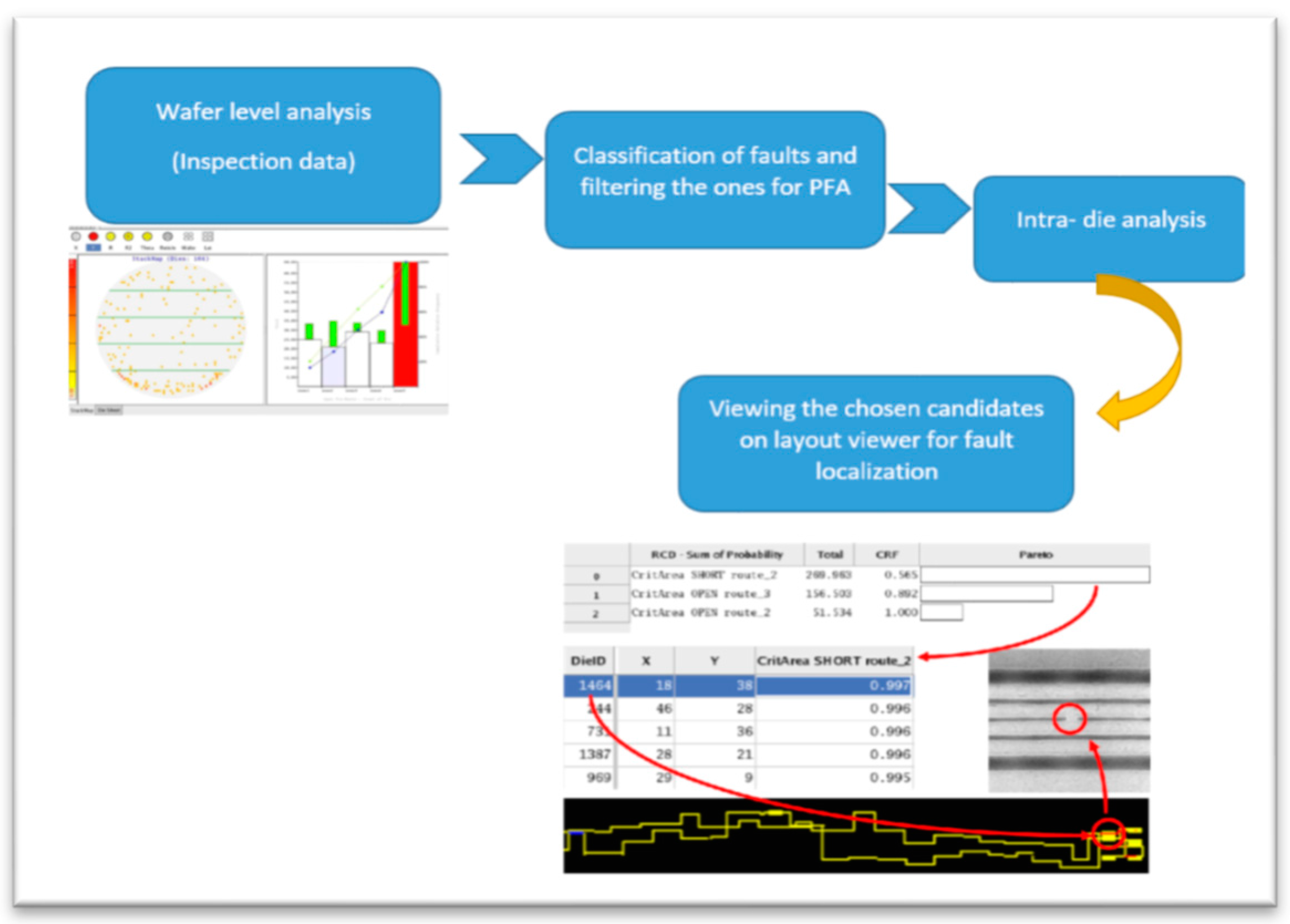
Figure 22.
(a) CAD design (b) CAD overlay on FIB-SEM (c) FIB-trench created using the guidance of CAD (d) Backside image of FIB-trench. No circuit features visible—only CAD polygons of the active diffusion layer.
Figure 22.
(a) CAD design (b) CAD overlay on FIB-SEM (c) FIB-trench created using the guidance of CAD (d) Backside image of FIB-trench. No circuit features visible—only CAD polygons of the active diffusion layer.

Figure 23.
Typical FA flow diagram, showing where FIB-SEMs are typically used.

Figure 24.
Use flow with FIB (a) Top cell view of IC layout (b) Zoomed in view of diagnostics net (c) Cross-mapped net to schematic view (d) Identifying the Fibable regions in layout.
Figure 24.
Use flow with FIB (a) Top cell view of IC layout (b) Zoomed in view of diagnostics net (c) Cross-mapped net to schematic view (d) Identifying the Fibable regions in layout.


Figure 25.
FIB candidate on diagnostics net.

Figure 26.
3D View with FIB simulation.

Figure 27.
Syncing FIB image with layout for PFA process.
© 2018 by the authors. Licensee MDPI, Basel, Switzerland. This article is an open access article distributed under the terms and conditions of the Creative Commons Attribution (CC BY) license (http://creativecommons.org/licenses/by/4.0/).
Share and Cite
MDPI and ACS Style
Oberai, A.; Yuan, J.-S. Efficient Fault Localization and Failure Analysis Techniques for Improving IC Yield. Electronics 2018, 7, 28. https://doi.org/10.3390/electronics7030028
AMA Style
Oberai A, Yuan J-S. Efficient Fault Localization and Failure Analysis Techniques for Improving IC Yield. Electronics. 2018; 7(3):28. https://doi.org/10.3390/electronics7030028
Chicago/Turabian StyleOberai, Ankush, and Jiann-Shiun Yuan. 2018. "Efficient Fault Localization and Failure Analysis Techniques for Improving IC Yield" Electronics 7, no. 3: 28. https://doi.org/10.3390/electronics7030028
Note that from the first issue of 2016, this journal uses article numbers instead of page numbers. See further details here.