A 6-Bit 0.13 μm SiGe BiCMOS Digital Step Attenuator with Low Phase Variation for K-Band Applications
by
Muhammad Masood Sarfraz
1,2,3, 
Farman Ullah
1,2,3,
Minghua Wang
1,2,
Haiying Zhang
1,2 and
Yu Liu
1,2,* 1
Institute of Microelectronics, Chinese Academy of Sciences, Beijing Key Laboratory of Radio Frequency IC Technology for Next Generation Communications, Beijing 100029, China
2
Institute of Microelectronics, University of Chinese Academy of Sciences (UCAS), 19A Yuquan Rd., Shijingshan District, Beijing 100049, China
3
COMSATS University, Wah Campus G. T. Road, Wah Cantt 47040, Pakistan
*
Author to whom correspondence should be addressed.
Electronics 2018, 7(5), 74; https://doi.org/10.3390/electronics7050074
Submission received: 29 March 2018
/
Revised: 3 May 2018
/
Accepted: 7 May 2018
/
Published: 17 May 2018
Abstract
:This paper presents the design and measuring of a 6-bit SiGe BiCMOS digital step attenuator, with a maximum attenuation of 31.5 dB, and with 0.5 dB steps (64 states) that have the lowest RMS amplitude error and a low phase variation. To alleviate the large phase variation of the conventional attenuator at a higher frequency, the proposed attenuator utilizes a phase compensation circuit. The phase compensation circuit consists of a 2nd order low pass phase correction network, stacked in parallel to the switched π/T structure of each attenuation module. An attenuator with a phase compensation network shows a root mean square (RMS) amplitude error less than 0.43 dB, and the RMS insertion phase deviation varying from 1.6° to 4.2° over 20–24 GHz. The measured insertion loss is 21.9 dB and the input P1dB is 14.03 dBm at 22 GHz. Our confidence regarding the obtained results stems from a comparison of simulations, carried out using Cadence Virtuoso, and physical measurements using a network analyzer (also presented). The proposed attenuator’s design has a 0.13 μm SiGe BiCMOS process, with an approximate occupied area of 1.92 × 0.4 mm2 including chip pads.
1. Introduction
In modern communication systems, a digital step attenuator is an essential part of the transceiver modules of phased array antenna and beamforming systems [1,2,3]. In phased-array systems, typically, attenuators are developed with low insertion phase variations over different attenuation states. In addition, the incoming signal arriving at the attenuators is usually very large, and the attenuator must have high enough linearity to handle the large signal, as well as a low insertion phase variation. For the systems to provide low insertion phase and get the desired amplitude, the phase and amplitude of the incoming signal must be accurately set. Particularly, in the case where several Transmit/Receive (T/R) modules are integrated, the exact phase and amplitude values are required [4,5,6,7].
Conventionally, Variable Gain Amplifiers (VGAs) were used to produce variable gain outputs at the expense of high power consumption and poor linearity. In addition, these approaches were not suitable for mm-Wave applications. An attenuator can overcome these problems and potentially provide better performance for wide-band applications, such as mobile and vehicular communications. Furthermore, the improved scaling of CMOS and SiGe technologies can guarantee the design of high-performance attenuators that are appropriate for high-frequency applications [8,9,10].
The stringent parameters are, to design an attenuator with high linearity, low phase and amplitude error, wideband and larger attenuation range. Various attenuator topologies are reported before for mm-Wave applications, such as switched path attenuators [11], switched π/T attenuators [12] and distributed step attenuators [13,14]. Although the topology reported by Sjogren et al. [11] is an appropriate choice for a system that provides low phase variation, Single Pole Double Throw (SPDT) switches experience high insertion losses at the reference state, due to their cumulative losses. In addition, the implementation of SPDT switches, when implemented for multi-bit designs, required more area. A distributed step attenuator on the other hand, may offer optimal source/load matching with a lower insertion loss. However, it is not an area or cost-effective solution and thus its application is limited. Switched π/T attenuators are a series and shunt resistive combination, using switches for attenuation. However, in the K-band frequency, it is very challenging to achieve the desired attenuation and low phase/amplitude error simultaneously [14].
This work presents a 6-bit digital step attenuator designed in a 0.13 μm SiGe BiCMOS process for low insertion phase variations, higher attenuation and larger bandwidth, employing 2nd order capacitive phase correction network. The proposed attenuator design consists of six attenuation modules with weighted attenuation of 0.5, 1, 2, 4, 8 and 16 dB. Bridge-T configuration is used for lower attenuation bits i.e., 0.5, 1, 2 and 4 dB, while π-topology is used for higher attenuation bits, i.e., 8 and 16 dB. Section 2 analyzes the proposed circuit design and explains that how the limitations in the conventional design are removed, using the proposed phase correction network. Results and comparison of the proposed attenuator, with various other, previously published attenuators are discussed in Section 3 and Section 4, respectively. Finally, this work is concluded in Section 5.
2. Design of the Attenuator
2.1. NMOS Switch
The conventional design of the switched π-type attenuators consists of switches and resistors, connected in series and parallel. The nMOS transistor, as one of the key components of a digital step attenuator, can be typically used as a switch. It contributes series on resistance when it is turned on and series off-capacitance when it is off, while passing the incoming signal from input to output. When the switch is ON, as shown by the equivalent circuit model in Figure 1a, it works like a resistor, and its R on can be estimated using Equation (1) [15,16]. The off-capacitance of the switch is also demonstrated using its equivalent circuit model in Figure 1b.
Note that on-resistance changes with varying the size of a transistor. For example, when a transistor with a large gate-width is used, it contributes less resistance and the R_on works as a short path, if a sufficiently large gate width transistor is used for the signal passing from input to the output. However, in a switched-off state, the switch behaves like a capacitive network and provides a leakage path to the signal. The parasitic-like gate-Source/Drain (CGS, CGD) makes a forward path to the signal and results in a phase lead. In addition, the junction capacitances, as shown in Figure 1, provide the leakage path to the body. These parasitics cause phase differences due to the phase-lead characteristics of the capacitor. In addition, the undesirable junction capacitances may also be the part of input/output matching networks that affect overall system matching. Consequently, a poor matching results in a large insertion loss. These leakage paths waste the signal power when the signal is transmitted from input to output. This event, in turn, increases the insertion loss of the attenuator. To overcome these losses, a large resistor to the gate of the nMOS switch is connected.
Due to the combination of series and shunt resistance, each attenuator’s amplitude will be switched between the minimum and maximum attenuation states. The desired attenuation can be achieved by choosing an appropriate value of a resistor in each attenuator, to realize the desired attenuation amplitude of each respective attenuator. The value of each resistor can be calculated using two-port network analysis [17].
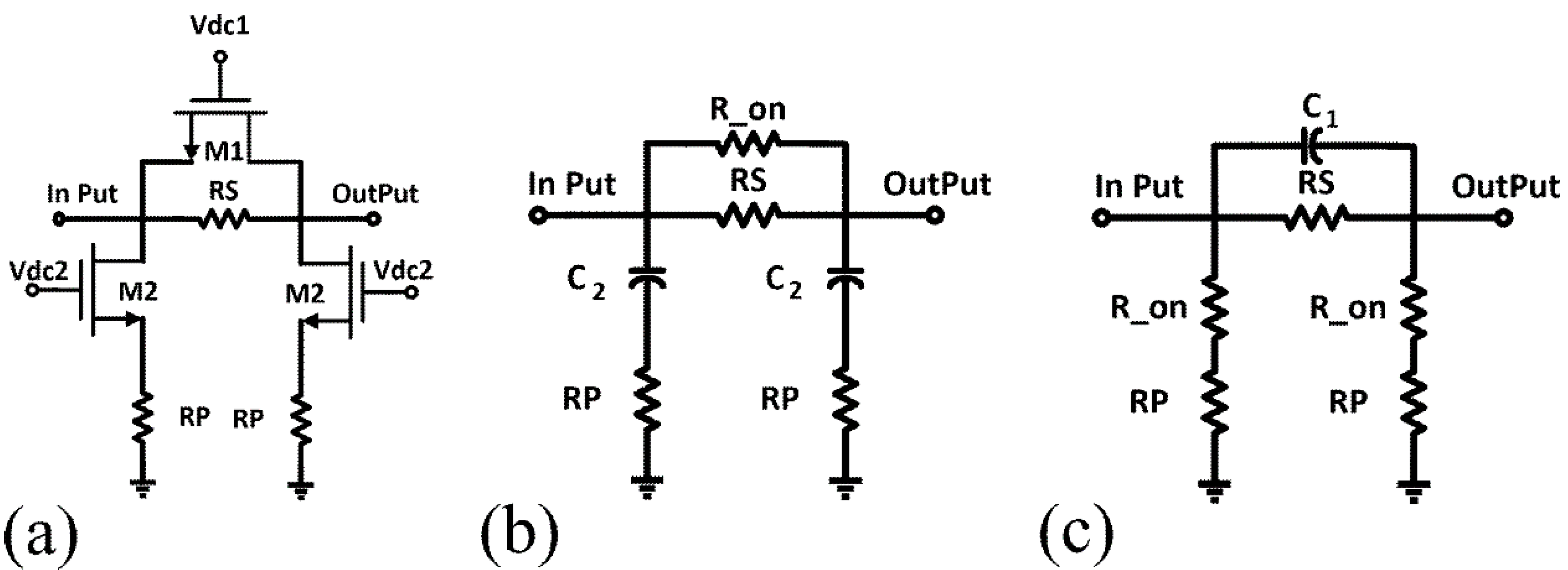
2.2. Conventional Attenuator Design
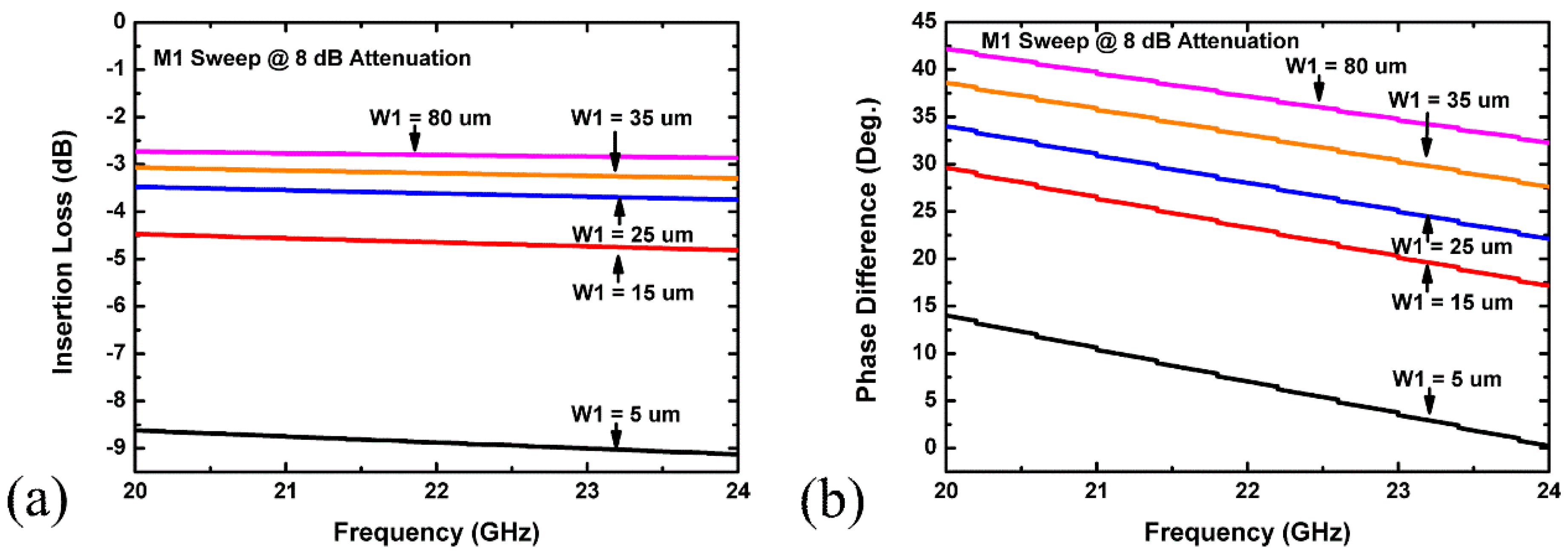
Figure 2a depicts the traditional π-attenuator, and parts (b) and (c) of the figure represent the reference and attenuation states comprising equivalent series and shunt resistances. As the width of M1 in Figure 2a scales up, the ON-resistance decreases as suggested by Equation (1). Likewise, transistor sizing additionally affects the performance of the attenuator. Consider the simulation results shown in Figure 3 for an 8-dB attenuator of the conventional structure: As the gate width of M1 increases, the insertion phase increases, while insertion loss decreases, making it impossible to optimize both simultaneously.
It is important to satisfy Equation (2) in order to minimize the phase difference between the attenuator’s two states, where is the transmission phase at reference state and is the transmission phase at attenuation state [17].
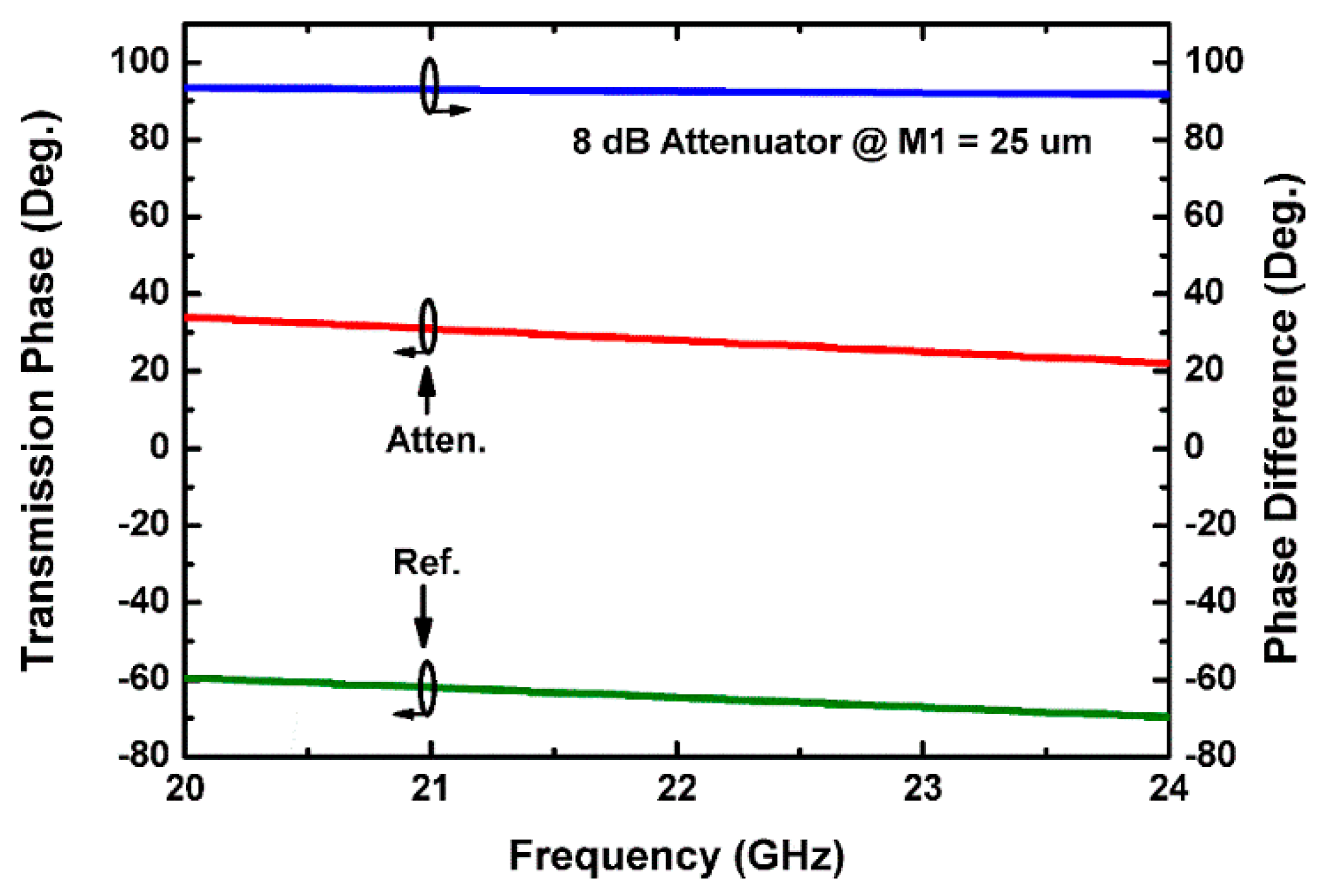
To have zero phase difference, the switch-off capacitances C1 and C2 of series and shunt transistors respectively shown in Figure 2 must ideally be zero. However, it is challenging in that these capacitance contribute zero value at high frequencies since the capacitive part is very significant at K-band. This event is why the observed phase difference is large, as depicted in Figure 4.
2.3. Proposed an Attenuator Design
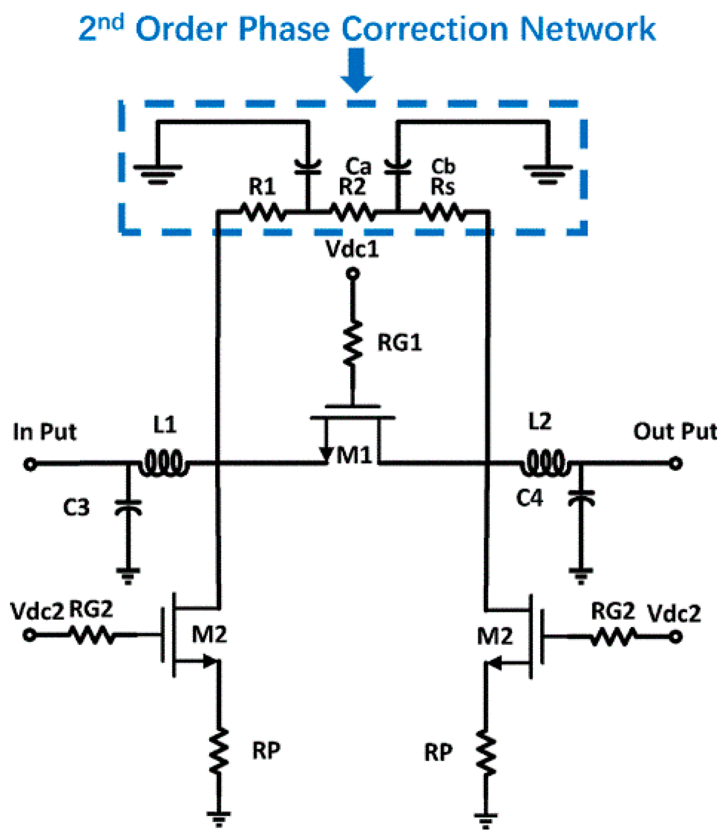
We believe a low pass filter, with phase lag characteristics can be used to minimize the transmission phase difference [4,17,18], which essentially depends on series capacitances Ca and Cb of the proposed phase correction network within the π-type attenuator, shown in Figure 5.
Figure 6a presents behavior of the phase difference in response to variations in the two capacitances, between 0 and 130 fF. By carefully selecting these capacitances with appropriate transistor sizing, we can obtain a minimal insertion phase at the desired frequency. This achievement can also be verified for an 8-dB attenuator using simulations, shown in Figure 6b, where the phase difference between reference and attenuation approaches almost zero.
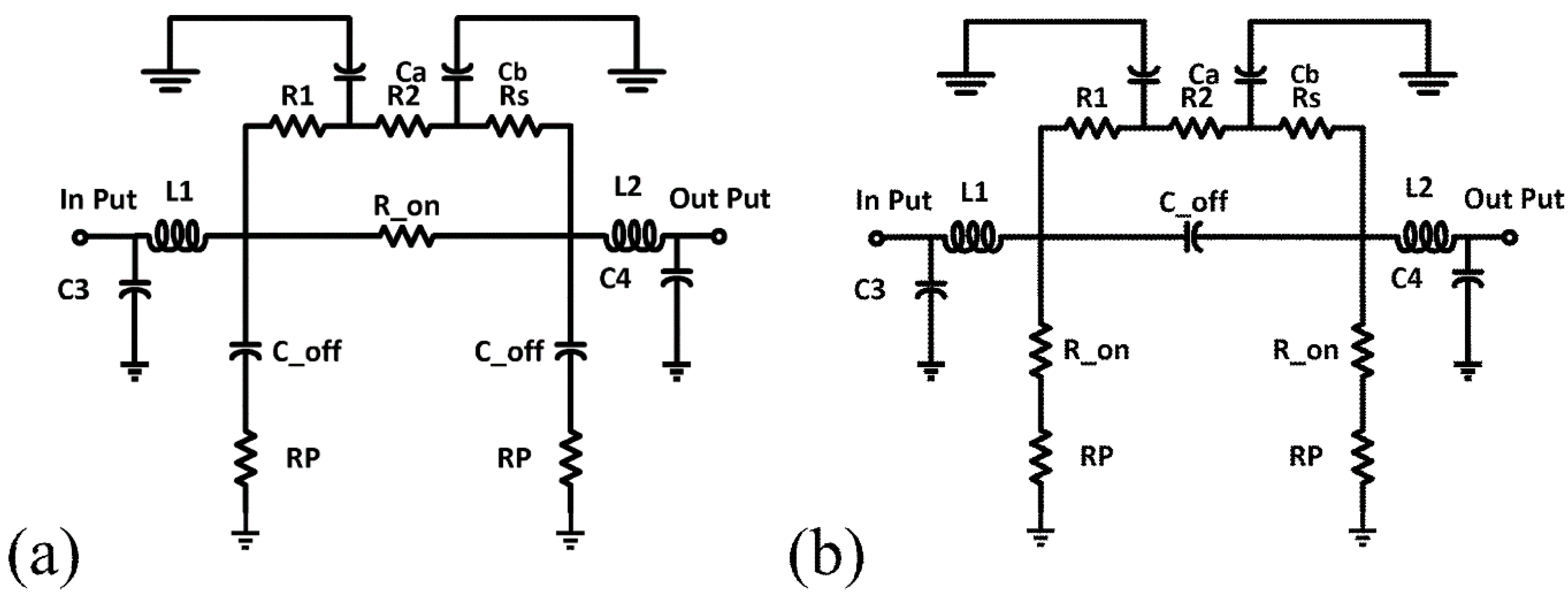
To attain confidence in this phase correction structure, we augmented it with the conventionally used attenuator. Although the transmission phase difference was indeed optimized, the attenuation level was reduced as well. The desired attenuation level was then achieved by connecting Rs in series with the proposed network, as shown in Figure 7 [17]. Note that parts (a) and (b) of the figure show the reference and attenuation states, respectively.
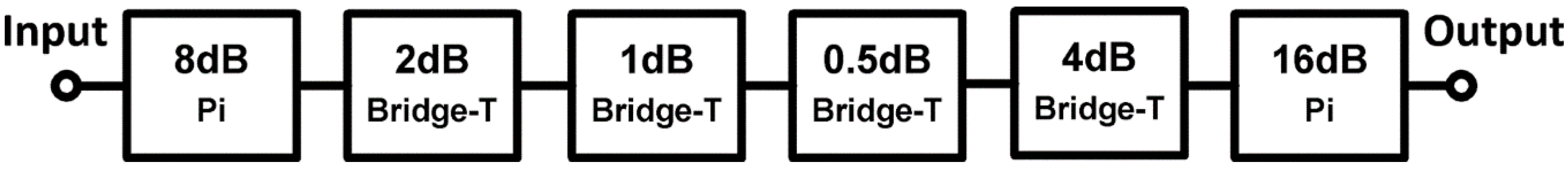
The proposed model of a 6-bit digital step attenuator is an extended version of our previously designed 4-bit digital step attenuator, simulated in the range of 31–33 GHz [18]. In contrast, the 6-bit attenuator is designed for systems that require higher attenuation, i.e., 31.5 dB with a minimum phase error, and is simulated in the range of 20–24 GHz, consisting of 64 attenuation states and cascaded in the sequence of 8, 2, 1, 0.5, 4 and 16 dB, as shown in Figure 8. Note that for larger attenuations, we have adopted Pi configuration, whereas Bridged-T configuration is chosen for smaller ones, as depicted in Figure 9. Conversely, the 4-bit attenuator merely exploits the bridge-T type attenuator [18]. Furthermore, the 6-bit attenuator which is an extension of our previous work is to implement a higher bit mm-Wave digital step attenuator on silicon-based technology.
The component values of each attenuator module are summarized in Table 1.
To acquire good impedance matching, an LC matching network is used between every two attenuators. As mentioned earlier, for the desired attenuation level and returns losses, careful transistor sizing, and selection of appropriate components values are essential so that every bit should attain the corresponding attenuation value—once the latter changes from the reference to the maximum states. Moreover, proper matching of the input-output reflection coefficient is essential for an acceptable accuracy of attenuation results.
3. Measured Results
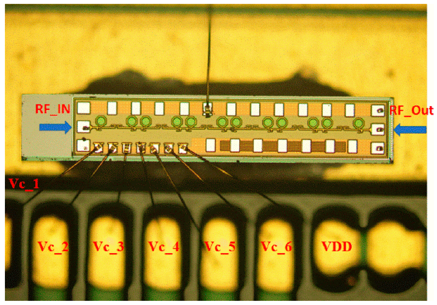
Figure 10 depicts a micro photograph of the proposed 6-bit digital step attenuator, including matching network between every two blocks. The prototypes input and output ports are indicated as RF_IN and RF_OUT respectively. The controlling terminal of each attenuator bit is denoted as VC1-6. The attenuator was fabricated using 0.13 μm SiGe BiCMOS process, and the total chip size including pad was 1.92 × 0.4 mm2. The simulation of the circuit was carried out using a tool, Cadence Virtuoso, while Peak View EM tool (Lorentz Solution, Santa Clara, CA, USA) was used for the EM simulations of the interconnects and major RF lines. The testing of a chip was executed, using Cascade Microtech’s GSG probe (Beaverton, OR, USA) and Agilent’s network analyzer (Santa Rosa, CA, USA). A DC voltage of 1.2 V was used for the gate control.
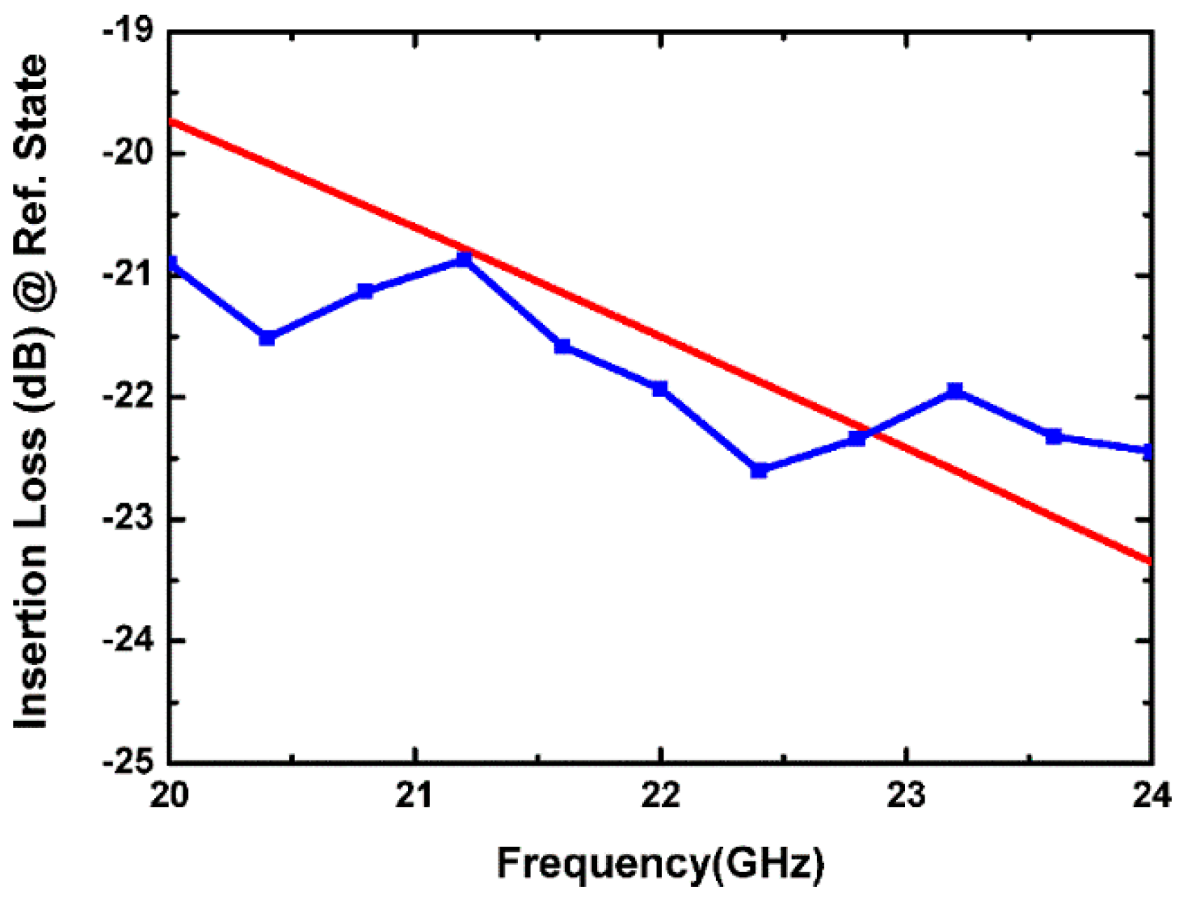
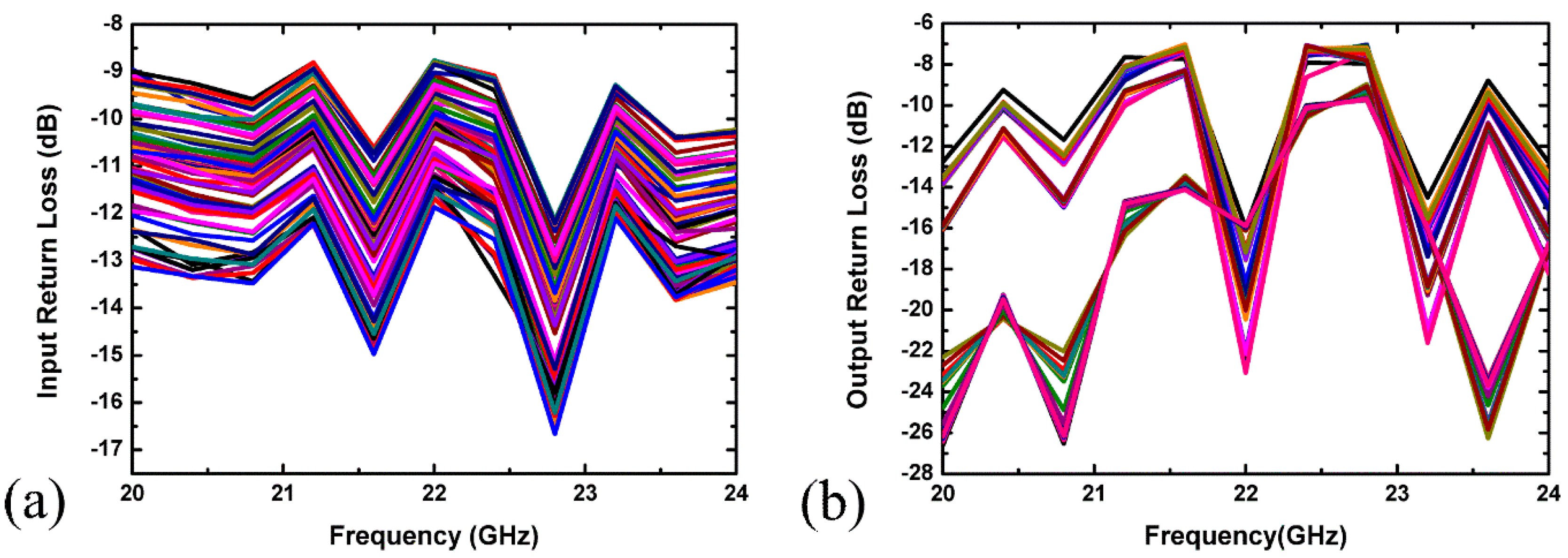
Figure 11 depicts the insertion loss against the applied frequency of the proposed 6-bit digital step attenuator, which was 20.9–21.95 dB in the range of 20–24 GHz. The measured return losses for both input and output of all the attenuation states were terminated with 50 Ω load impedance, as shown in Figure 12. The input return losses were lower than −9 dB, while the output return losses were less than −7 dB for the 20–24 GHz range.
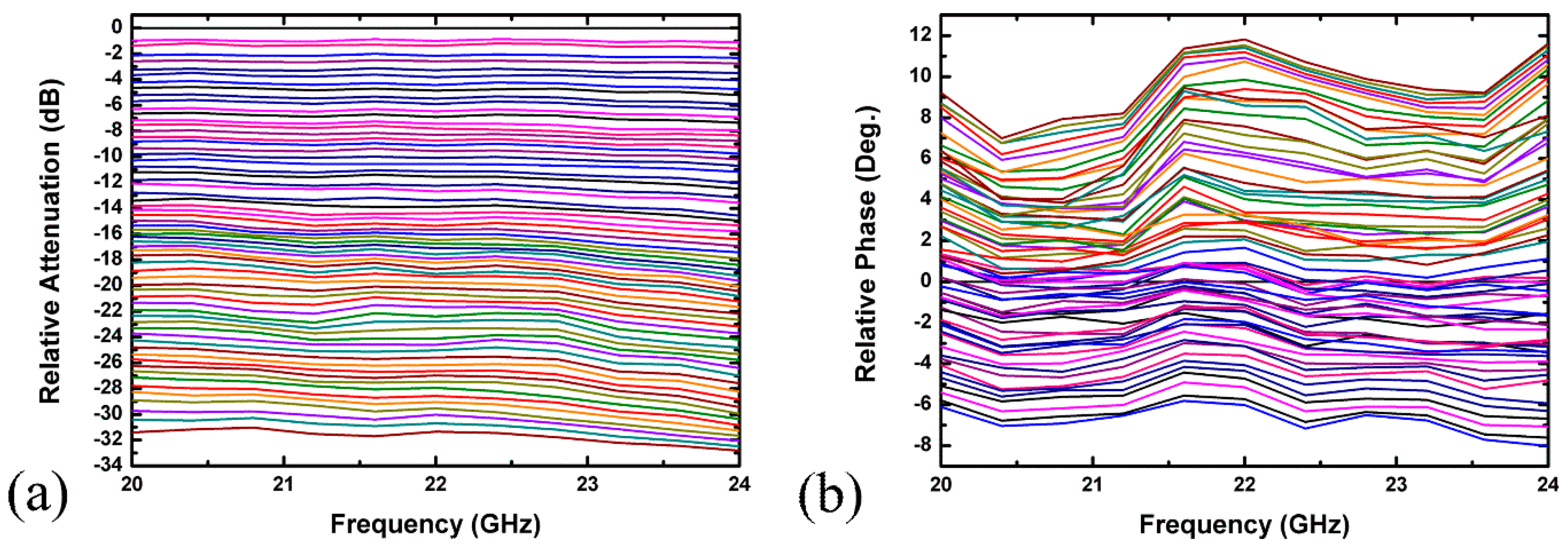
Figure 13a,b demonstrates the normalized attenuation and phase plots, relative to their respective reference states, attaining a maximum attenuation of 31.5 ± 0.5 dB in the targeted frequency range of 20–24 GHz. The measured RMS amplitude and phase errors were then plotted against the simulation results in Figure 14 for comparison purposes. The measured root mean square (RMS) amplitude error deviation was less than 0.43 dB over 20–24 GHz, which is in close agreement with the simulated results. However, the measured RMS phase error was a little more off from the simulation results and shows about a 1–5-degree difference between simulation and measured results. This may be due to the following possible reasons.
- Process variations can cause a phase difference between the measured and simulated results because each process has its own resistance and capacitance variations up to the order of ±10%. Therefore, a cumulative effect of the process variation results in the form of overall capacitance of the system, which leads to a large phase error. The capacitance effect on the phase is also illustrated in Figure 6a,b.
- As mentioned in Section 2.3, the optimum component values of the capacitive phase correction network are very important to get the minimum phase error. Therefore, a minor contribution of parasitics (due to the testing hardware, external environment, etc.) can cause significant deviation from the targeted results and consequently, it appears in the form of large phase error.
However, in our targeted frequency range—i.e., from 20–24 GHz, the measured RMS phase error—and by comparing with other state-of-the-art reported articles listed in Table 2, the proposed technique achieved the least phase errors. The measurement results show that the proposed designed attenuator can be efficiently used for K-band applications, having the frequency range of 20–24 GHz for a controlled amplitude and phase.
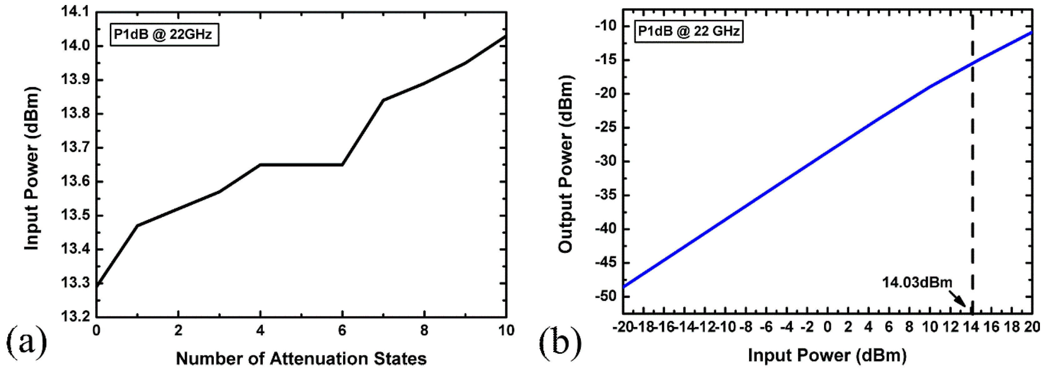
Figure 15 describes the compression point P1dB simulation results in different attenuation states at 22 GHz. It shows that the proposed attenuator has an input P1dB of 14.03 dBm.
4. Comparison with Other Technology Attenuators
Table 2 compares the performance of attenuators reported in the most recently published articles [6,8,9,12,17,18,19]. Compared with the GaAs attenuators [6,8,9,12], the proposed attenuator has the highest attenuation of 31.5 dB and the best resolution of 0.5 dB. Additionally, the proposed model has the lowest phase variation along with the smallest chip size, at the frequency range of 20–24 GHz. In addition, if we compare our work with Sarfraz et al. [18], more bits were accommodated in the same die area with improved RMS amplitude and phase error. The insertion losses were higher and P1dB values were lower than those of the GaAs attenuators, due to the relatively poor performance of the CMOS transistor. To the best of our knowledge, we believe the proposed design is the first of its kind that uses 0.13 μm SiGe BiCMOS attenuator for K-band applications.
5. Conclusions
In this brief, we have designed and measured the 6-bit digital step attenuator for K-band application. The attenuator is implemented with a second-order phase correction network, to mitigate the insertion phase that previously occurred in the conventional design. The attenuator with proposed method shows less than 0.43 dB/1.6–4.2° RMS amplitude/phase error over 20–24 GHz. The 6-bit digital step attenuator with a phase correction network was fabricated in 0.13 μm SiGe BiCMOS technology. The attenuator has the highest attenuation range of 31.5 dB over 20–24 GHz with the highest resolution of 0.5 dB. The return losses are lower than −9 dB and −7 dB at 20–24 GHz. The insertion loss is 20.9–21.95 dB for the said frequency range. Chip size is 1.92 × 0.4 mm2. The results show that the attenuator has good performance when compared to the listed GaAs attenuators in Table 2 for 20–24 GHz applications with higher attenuation range, phase accuracy, and compact chip area.
Author Contributions
M.M.S. and M.W. conceived, designed, and performed the experiments. M.M.S., Y.L., F.U. and M.W. analyzed the data and wrote the manuscript. H.Z. and Y.L. supervised the research and revised the manuscript. All authors discussed the results and commented on the manuscript.
Acknowledgments
This work is supported by National Science Foundation of China (grant number: 61574165), and CAS-TWAS President’s Fellowship for Muhammad Masood Sarfraz (Student ID: 2013A8011207116). The authors would like to thank the Global Foundries for the fabrication and Lorentz Solution for Peak View EM Design support.
Conflicts of Interest
The authors declare no conflict of interest.
References
- Ellinger, F.; Vogt, R.; Bachtold, W. Calibratable adaptive antenna combiner at 5.2 GHz with high yield for laptop interface card. IEEE Trans. Microw. Theory Tech. 2000, 48, 2714–2720. [Google Scholar] [CrossRef]
- Dogan, H.; Meyer, R.G. Intermodulation distortion in CMOS attenuators and switches. IEEE J. Solid State Circuits 2007, 42, 529–539. [Google Scholar] [CrossRef]
- Ku, B.H.; Hong, S. 6-bit CMOS digital attenuators with low phase variations for X-band phased-array systems. IEEE Trans. Microw. Theory Tech. 2010, 58, 1651–1663. [Google Scholar] [CrossRef]
- Sun, P. Analysis of phase variation of CMOS digital attenuator. Electron. Lett. 2014, 50, 1912–1914. [Google Scholar] [CrossRef]
- Zhang, H.; Wan, C.; Zhu, D. In A high linearity digital attenuator with low phase variations for x-band phased array systems. In Proceedings of the 2016 IEEE International Conference on Microwave and Millimeter Wave Technology (ICMMT), Beijing, China, 5–8 June 2016; pp. 173–175. [Google Scholar]
- Ciccognani, W.; Giannini, F.; Limiti, E.; Longhi, P.E. Compensating digital attenuator differential phase shift. In Proceedings of the 2008 14th Conference on Microwave Techniques, Prague, Czech Republic, 23–24 April 2008; pp. 1–4. [Google Scholar]
- Ciccognani, W.; Giannini, F.; Limiti, E.; Longhi, P.E. Compensating for parasitic phase shift in microwave digitally controlled attenuators. Electron. Lett. 2008, 44, 743–744. [Google Scholar] [CrossRef]
- Dogan, H.; Meyer, R.G.; Niknejad, A.M. Analysis and design of RF CMOS attenuators. IEEE J. Solid State Circuits 2008, 43, 2269–2283. [Google Scholar] [CrossRef]
- Kaunisto, R.; Korpi, P.; Kiraly, J.; Halonen, K. In A linear-control wide-band CMOS attenuator, ISCAS 2001. In Proceedings of the 2001 IEEE International Symposium on Circuits and Systems (Cat. No.01CH37196), Sydney, Australia, 6–9 May 2001; Volume 454, pp. 458–461. [Google Scholar]
- Bae, J.; Lee, J.; Nguyen, C. A 10-67GHz CMOS dual-function switching attenuator with improved flatness and large attenuation range. IEEE Trans. Microw. Theory Tech. 2013, 61, 4118–4129. [Google Scholar] [CrossRef]
- Sjogren, L.; Ingram, D.; Biedenbender, M.; Lai, R.; Allen, B.; Hubbard, K. A low phase-error 44-GHz HEMT attenuator. IEEE Microw. Guided Wave Lett. 1998, 8, 194–195. [Google Scholar] [CrossRef]
- Inkwon, J.; Youn-Sub, N.; In-Bok, Y. In Ultra broadband dc to 40 GHz 5-bit pHEMT MMIC digital attenuator. In Proceedings of the 2005 European Microwave Conference, Paris, France, 4–6 October 2005. [Google Scholar]
- Hunton, J.K.; Ryals, A.G. Microwave variable attenuators and modulators using pin diodes. IRE Trans. Microw. Theory Tech. 1962, 10, 262–273. [Google Scholar] [CrossRef]
- Min, B.W.; Rebeiz, G.M. A 10–50 GHz CMOS distributed step attenuator with low loss and low phase imbalance. IEEE J. Solid State Circuits 2007, 42, 2547–2554. [Google Scholar] [CrossRef]
- Razavi, B.; Behzad, R. RF Microelectronics, 2nd ed.; Prentice Hall: Upper Saddle River, NJ, USA, 1998; ISBN 978-0-13-713473-1. [Google Scholar]
- Meyer, R.G.; Mack, W.D. A wideband low-noise variable-gain BiCMOS transimpedance amplifier. IEEE J. Solid State Circuits 1994, 29, 701–706. [Google Scholar] [CrossRef]
- Zhang, Y.; Zhuang, Y.; Li, Z.; Ren, X.; Wang, B.; Jing, K.; Qi, Z. A 5-bit lumped 0.18-μm CMOS step attenuator with low insertion loss and low phase distortion in 3–22GHz applications. Microelectron. J. 2014, 45, 468–476. [Google Scholar] [CrossRef]
- Sarfraz, M.M.; Liu, Y.; Ullah, F.; Wang, M.; Zhang, H. 4-Bit Ka band SiGe BiCMOS digital step attenuator. PIER Prog. Electromagn. Res. C 2017, 74, 31–40. [Google Scholar] [CrossRef]
- Bae, J.; Nguyen, C. A novel concurrent 22–29/57–64-ghz dual-band CMOS step attenuator with low phase variations. IEEE Trans. Microw. Theory Tech. 2016, 64, 1867–1875. [Google Scholar] [CrossRef]
Figure 1.
Equivalent circuit model of nMOS switch (a) at R_on State; (b) at C_off State.

Figure 2.
The conventional structure of (a) π -type attenuator with (b) reference and (c) attenuation state.
Figure 2.
The conventional structure of (a) π -type attenuator with (b) reference and (c) attenuation state.

Figure 3.
Eight decibel π-type attenuator simulation result: (a) insertion loss; (b) phase difference.
Figure 3.
Eight decibel π-type attenuator simulation result: (a) insertion loss; (b) phase difference.

Figure 4.
Eight decibel conventional π-type attenuator simulation result of transmission phase and phase difference.
Figure 4.
Eight decibel conventional π-type attenuator simulation result of transmission phase and phase difference.

Figure 5.
The proposed structure of π-type attenuator.

Figure 6.
Proposed 8 dB π-type attenuator simulation results: (a) proposed structure phase difference under different values of Ca and Cb; (b) phase difference and transmission phase.
Figure 6.
Proposed 8 dB π-type attenuator simulation results: (a) proposed structure phase difference under different values of Ca and Cb; (b) phase difference and transmission phase.
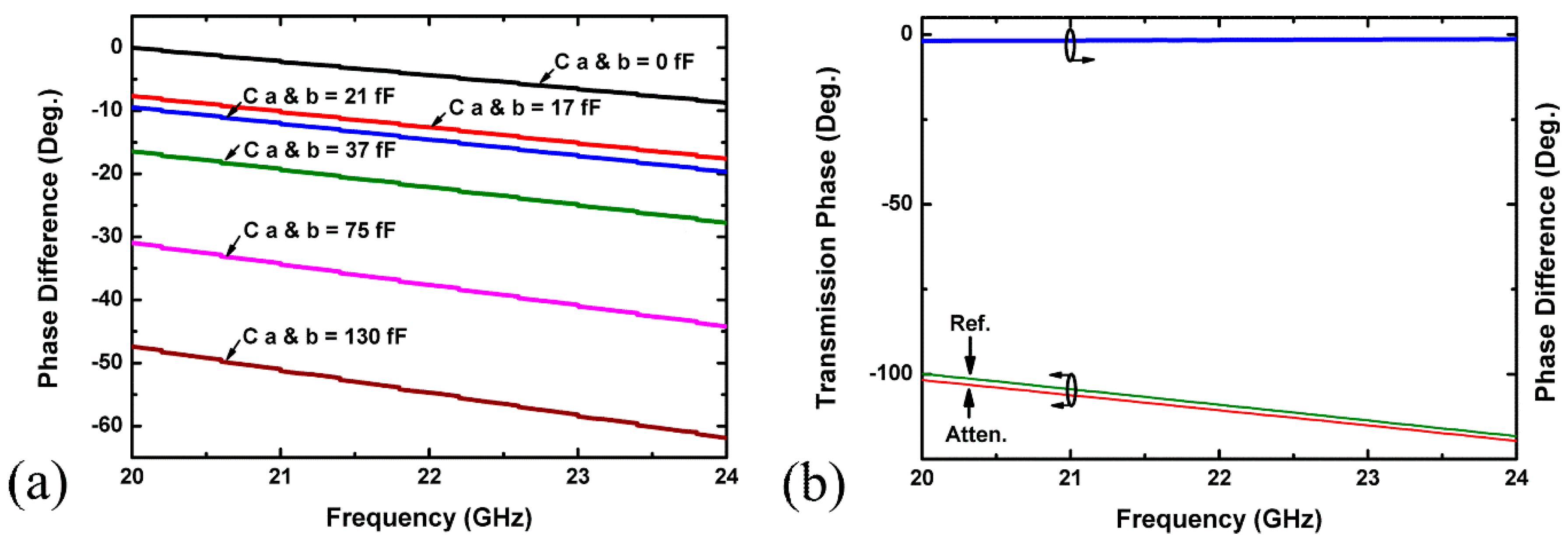
Figure 7.
Proposed design (a) Reference State; (b) Attenuation State.

Figure 8.
Bit ordering of the proposed 6-bit digital step attenuator.

Figure 9.
Proposed attenuator: (a) Bridge-T attenuator for lower attenuation (0.5 dB, 1 dB, 2 dB and 4 dB) and (b) Pi attenuator for higher attenuation (8 dB and 16 dB).
Figure 9.
Proposed attenuator: (a) Bridge-T attenuator for lower attenuation (0.5 dB, 1 dB, 2 dB and 4 dB) and (b) Pi attenuator for higher attenuation (8 dB and 16 dB).

Figure 10.
Micro graph of 6-bit digital step attenuators.

Figure 11.
Measured and simulated insertion loss in the reference state.

Figure 12.
(a) Measured input return loss; (b) measured output return loss.

Figure 13.
Measured: (a) relative attenuation; (b) relative phase plots of 6-bit digital step attenuator.
Figure 13.
Measured: (a) relative attenuation; (b) relative phase plots of 6-bit digital step attenuator.

Figure 14.
Measured and simulated (a) RMS amplitude error and (b) RMS phase error.

Figure 15.
Input P1dB (a) simulation result at different attenuation states; (b) of the proposed attenuator at 22 GHz.
Figure 15.
Input P1dB (a) simulation result at different attenuation states; (b) of the proposed attenuator at 22 GHz.


Table 1.
Component values of 6-bit attenuators.
| Atten. (dB) | Topology | R1 = R2 (Ω) | RP (Ω) | W1 (μm) | W2 (μm) | Ca = Cb (F) |
|---|---|---|---|---|---|---|
| 0.5 | Bridge-T | 3 | 211 | 10 | 20 | 17 |
| 1 | Bridge-T | 6 | 134 | 10 | 20 | 17 |
| 2 | Bridge-T | 10 | 236 | 65 | 20 | 17 |
| 4 | Bridge-T | 34 | 78 | 60 | 15 | 70 |
| 8 | π-Type | 60 | 124 | 25 | 15 | 37 |
| 16 | π-Type | 47 | 29 | 15 | 20 | 29 |
Table 2.
Proposed digital step attenuator performance summary.
| References | [6] | [8] | [9] | [12] | [17] | [18] | [19] | This Work |
|---|---|---|---|---|---|---|---|---|
| Frequency (GHz) | 8–15 | 0.1–20 | Dc-18 | Dc-20 | 3–22 | 31–33 | 22–29 | 20–24 GHz |
| Attenuation Range (dB) | 23.5 (6-Bit) (LSB = 0.5 dB) | 23 (5-Bit) (LSB = 0.5 dB) | 27.9 (5-Bit) (LSB = 0.9 dB | 23.5 (5-Bit) (LSB = 0.5 dB | 31 (5-Bit) (LSB = 1 dB) | 16 (4-Bit) (LSB = 0.5 dB) | 16 (4-Bit) (LSB = 1 dB) | 31.5 (6-Bit) (LSB = 0.5 dB |
| Insertion Loss (dB) | <4.5 | 3–5 | 3–7 | <5 | 5.53–13.7 | <19 | 5.4–7.9 | 20.9–21.95 |
| Return Loss (dB) | >8 | >15 | >17 | >13 | >11 | >12.7 | N/A | >9 |
| RMS Attenuation Error (dB) | <0.45 | <1 | <0.5 | <0.5 | <0.53 | <0.8 | <0.51 | <0.43 |
| RMS Phase Error (Degree°) | N/A | 0.1–20 | 0–18 | N/A | 6.3 | 2.8–5.8 | 1–4.7 | 1.6–4.2 |
| Input P1dB (dBm) | N/A | 26 | 24 | 24 | 18.4 | N/A | 14 | 14 |
| Structure | Switched π/T | N/A | Switched T | Switched T | Switched π/T | Switched T | Switched π/T | Switched π/T Bridge |
| Technology | GaAs | GaAs | GaAs | GaAs | 0.18 µm CMOS | 0.13 µm SiGe BiCMOS | 0.18 µm CMOS | 0.13 µm SiGe BiCMOS |
| Size (mm2) | 3 × 2 | 2.34 × 1.5 | 2.4 × 1.6 | 2.6 × 1.6 | 1.28 × 0.5 | 1.92 × 0.4 | 1.8 × 0.52 | 1.92 × 0.4 |
© 2018 by the authors. Licensee MDPI, Basel, Switzerland. This article is an open access article distributed under the terms and conditions of the Creative Commons Attribution (CC BY) license (http://creativecommons.org/licenses/by/4.0/).
Share and Cite
MDPI and ACS Style
Sarfraz, M.M.; Ullah, F.; Wang, M.; Zhang, H.; Liu, Y. A 6-Bit 0.13 μm SiGe BiCMOS Digital Step Attenuator with Low Phase Variation for K-Band Applications. Electronics 2018, 7, 74. https://doi.org/10.3390/electronics7050074
AMA Style
Sarfraz MM, Ullah F, Wang M, Zhang H, Liu Y. A 6-Bit 0.13 μm SiGe BiCMOS Digital Step Attenuator with Low Phase Variation for K-Band Applications. Electronics. 2018; 7(5):74. https://doi.org/10.3390/electronics7050074
Chicago/Turabian StyleSarfraz, Muhammad Masood, Farman Ullah, Minghua Wang, Haiying Zhang, and Yu Liu. 2018. "A 6-Bit 0.13 μm SiGe BiCMOS Digital Step Attenuator with Low Phase Variation for K-Band Applications" Electronics 7, no. 5: 74. https://doi.org/10.3390/electronics7050074
Note that from the first issue of 2016, this journal uses article numbers instead of page numbers. See further details here.